US6806110B2 - Monolithic multi-wavelength vertical-cavity surface emitting laser array and method of manufacture therefor - Google Patents
Monolithic multi-wavelength vertical-cavity surface emitting laser array and method of manufacture thereforDownload PDFInfo
- Publication number
- US6806110B2 US6806110B2US10/151,646US15164602AUS6806110B2US 6806110 B2US6806110 B2US 6806110B2US 15164602 AUS15164602 AUS 15164602AUS 6806110 B2US6806110 B2US 6806110B2
- Authority
- US
- United States
- Prior art keywords
- reflector
- forming
- vertical cavity
- different
- optical devices
- Prior art date
- Legal status (The legal status is an assumption and is not a legal conclusion. Google has not performed a legal analysis and makes no representation as to the accuracy of the status listed.)
- Expired - Fee Related
Links
Images


Classifications
- H—ELECTRICITY
- H01—ELECTRIC ELEMENTS
- H01S—DEVICES USING THE PROCESS OF LIGHT AMPLIFICATION BY STIMULATED EMISSION OF RADIATION [LASER] TO AMPLIFY OR GENERATE LIGHT; DEVICES USING STIMULATED EMISSION OF ELECTROMAGNETIC RADIATION IN WAVE RANGES OTHER THAN OPTICAL
- H01S5/00—Semiconductor lasers
- H01S5/40—Arrangement of two or more semiconductor lasers, not provided for in groups H01S5/02 - H01S5/30
- H01S5/42—Arrays of surface emitting lasers
- H01S5/423—Arrays of surface emitting lasers having a vertical cavity
- H—ELECTRICITY
- H01—ELECTRIC ELEMENTS
- H01S—DEVICES USING THE PROCESS OF LIGHT AMPLIFICATION BY STIMULATED EMISSION OF RADIATION [LASER] TO AMPLIFY OR GENERATE LIGHT; DEVICES USING STIMULATED EMISSION OF ELECTROMAGNETIC RADIATION IN WAVE RANGES OTHER THAN OPTICAL
- H01S5/00—Semiconductor lasers
- H01S5/10—Construction or shape of the optical resonator, e.g. extended or external cavity, coupled cavities, bent-guide, varying width, thickness or composition of the active region
- H01S5/18—Surface-emitting [SE] lasers, e.g. having both horizontal and vertical cavities
- H01S5/183—Surface-emitting [SE] lasers, e.g. having both horizontal and vertical cavities having only vertical cavities, e.g. vertical cavity surface-emitting lasers [VCSEL]
- H01S5/18341—Intra-cavity contacts
- H—ELECTRICITY
- H01—ELECTRIC ELEMENTS
- H01S—DEVICES USING THE PROCESS OF LIGHT AMPLIFICATION BY STIMULATED EMISSION OF RADIATION [LASER] TO AMPLIFY OR GENERATE LIGHT; DEVICES USING STIMULATED EMISSION OF ELECTROMAGNETIC RADIATION IN WAVE RANGES OTHER THAN OPTICAL
- H01S5/00—Semiconductor lasers
- H01S5/10—Construction or shape of the optical resonator, e.g. extended or external cavity, coupled cavities, bent-guide, varying width, thickness or composition of the active region
- H01S5/18—Surface-emitting [SE] lasers, e.g. having both horizontal and vertical cavities
- H01S5/183—Surface-emitting [SE] lasers, e.g. having both horizontal and vertical cavities having only vertical cavities, e.g. vertical cavity surface-emitting lasers [VCSEL]
- H01S5/18358—Surface-emitting [SE] lasers, e.g. having both horizontal and vertical cavities having only vertical cavities, e.g. vertical cavity surface-emitting lasers [VCSEL] containing spacer layers to adjust the phase of the light wave in the cavity
- H—ELECTRICITY
- H01—ELECTRIC ELEMENTS
- H01S—DEVICES USING THE PROCESS OF LIGHT AMPLIFICATION BY STIMULATED EMISSION OF RADIATION [LASER] TO AMPLIFY OR GENERATE LIGHT; DEVICES USING STIMULATED EMISSION OF ELECTROMAGNETIC RADIATION IN WAVE RANGES OTHER THAN OPTICAL
- H01S5/00—Semiconductor lasers
- H01S5/10—Construction or shape of the optical resonator, e.g. extended or external cavity, coupled cavities, bent-guide, varying width, thickness or composition of the active region
- H01S5/18—Surface-emitting [SE] lasers, e.g. having both horizontal and vertical cavities
- H01S5/183—Surface-emitting [SE] lasers, e.g. having both horizontal and vertical cavities having only vertical cavities, e.g. vertical cavity surface-emitting lasers [VCSEL]
- H01S5/18361—Structure of the reflectors, e.g. hybrid mirrors
- H01S5/18363—Structure of the reflectors, e.g. hybrid mirrors comprising air layers
- H01S5/18366—Membrane DBR, i.e. a movable DBR on top of the VCSEL
- H—ELECTRICITY
- H01—ELECTRIC ELEMENTS
- H01S—DEVICES USING THE PROCESS OF LIGHT AMPLIFICATION BY STIMULATED EMISSION OF RADIATION [LASER] TO AMPLIFY OR GENERATE LIGHT; DEVICES USING STIMULATED EMISSION OF ELECTROMAGNETIC RADIATION IN WAVE RANGES OTHER THAN OPTICAL
- H01S5/00—Semiconductor lasers
- H01S5/10—Construction or shape of the optical resonator, e.g. extended or external cavity, coupled cavities, bent-guide, varying width, thickness or composition of the active region
- H01S5/18—Surface-emitting [SE] lasers, e.g. having both horizontal and vertical cavities
- H01S5/183—Surface-emitting [SE] lasers, e.g. having both horizontal and vertical cavities having only vertical cavities, e.g. vertical cavity surface-emitting lasers [VCSEL]
- H01S5/18361—Structure of the reflectors, e.g. hybrid mirrors
- H01S5/18369—Structure of the reflectors, e.g. hybrid mirrors based on dielectric materials
- H—ELECTRICITY
- H01—ELECTRIC ELEMENTS
- H01S—DEVICES USING THE PROCESS OF LIGHT AMPLIFICATION BY STIMULATED EMISSION OF RADIATION [LASER] TO AMPLIFY OR GENERATE LIGHT; DEVICES USING STIMULATED EMISSION OF ELECTROMAGNETIC RADIATION IN WAVE RANGES OTHER THAN OPTICAL
- H01S5/00—Semiconductor lasers
- H01S5/40—Arrangement of two or more semiconductor lasers, not provided for in groups H01S5/02 - H01S5/30
- H01S5/4025—Array arrangements, e.g. constituted by discrete laser diodes or laser bar
- H01S5/4087—Array arrangements, e.g. constituted by discrete laser diodes or laser bar emitting more than one wavelength
Definitions
- the present inventionrelates generally to vertical cavity lasers, and more specifically to monolithic arrays of vertical cavity lasers.
- VSELSVertical cavity surface emitting lasers
- VCSELshave relatively high efficiency, small size, low weight, low power consumption, and the capability to be driven by low-voltage power. They can operate in a single longitudinal mode, or frequency, and produce a circular beam of laser light that can easily be coupled into optical fibers.
- the surface emission featureallows devices to be packed densely on a wafer, so that two-dimensional arrays are fabricated relatively easily.
- VCSELSuse semiconductor materials comprised of elements such as aluminum, indium, gallium, arsenic, nitrogen, and phosphorous as the gain medium, and alternating high and low index of refraction materials such as silicon and silicon dioxide for the semiconductor mirrors or distributed Bragg reflectors (DBRs).
- elementssuch as aluminum, indium, gallium, arsenic, nitrogen, and phosphorous
- alternating high and low index of refraction materialssuch as silicon and silicon dioxide for the semiconductor mirrors or distributed Bragg reflectors (DBRs).
- DBRsdistributed Bragg reflectors
- the lasing wavelength of a VCSELis determined by the optical height of its resonant cavity. Most commonly the optical height, and thus the wavelength, is determined by the thicknesses of the semiconductor layers in the devices. These thicknesses are set during the growth of the semiconductor layers and are nominally the same for all the VCSELs on given wafer.
- the resonant cavity of some VCSELsalso includes an air gap, where the size of the air gap partly determines the lasing wavelength.
- a monolithic multiple-wavelength VCSEL arrayrequires side-by-side fabrication of VCSELs on a wafer where the VCSELs need to be exactly the same except with controlled, different lasing wavelengths. This presents a problem because the processing used on the wafer must assure that the threshold gain at which lasing begins, the current usage, the efficiency, the losses of light in the resonant cavity, the amplification of the gain material, and the light transmission of the DBR all remain the same. At the same time, the same processing must produce different lasing wavelengths, which is most commonly realized by changing the optical height of the resonant cavity.
- One prior art method to making a monolithic multiple wavelength VCSEL arrayis non-uniform growth due to thermal gradient.
- the backside of a substrateis patterned prior to epitaxial growth in a molecular beam epitaxy reactor.
- the resulting backside patternproduces a thermal gradient on the surface of the substrate when the wafer is heated.
- growth rateis temperature dependent, there is a variable material thickness and hence a variable laser wavelength along the thermal gradient.
- One disadvantage of this approachis the fact that the arrays are limited to linear geometries. To date, there have been problems controlling the wavelengths precisely and repeatedly over large areas of the wafer.
- An alternate prior art methodis laterally confining each laser prior to epitaxial growth by either etching a mesa or patterning windows in an oxide mask. This process is known as “selective area growth”. Growth rate and composition are functions of the lateral dimension. The method is problematic because it is sensitive to growth conditions and may vary from reactor to reactor or from growth to growth. In both of the aforementioned prior art methods, the proximity of different wavelength devices in an array is limited.
- Another prior art methodis to grow a partial VCSEL structure including the lower DBR, the gain material, and some part of the upper DBR.
- the waferis masked and anodically oxidized to some controlled oxide thickness over the exposed portions.
- a selective etchis then used to remove the oxide. This process is repeated to create different effective resonant cavity lengths for each laser in an array.
- the remainder of the VCSEL structureis regrown over the patterned wafer.
- each etchis sensitive to voltage and concentration variations that cause problems, which affect the depth, resulting in reduced control over wavelength spacing between devices.
- Another prior art methodis to grow a partial VCSEL structure including the lower DBR, the gain material, and a series of etch-stop layers that can be selectively etched away.
- the waferis repeatedly masked and etched so that different amounts of material are removed from the different VCSELs in the array.
- the waferis then re-introduced into the semiconductor growth apparatus and the deposition of the remaining layers is performed.
- This approachrequires multiple masking and etching steps to achieve the different etch depths. This becomes unmanageable when the number of VCSELs is greater than a few.
- this processrequires the upper portion of the semiconductor material must be epitaxially re-grown after the etching process is complete. This increases both the complexity and the cost of the fabrication process.
- the present inventionprovides a monolithic array of vertical cavity lasers with different emission wavelengths on a single wafer, and method of manufacture therefor.
- a first reflectoris over the semiconductor substrate with a photoactive semiconductor layer.
- a reflector supportdefines first and second air gaps with the photoactive semiconductor layer. The second and third air gaps are made to be different from each other by geometric differences in the reflector support structure.
- Second and third reflectorsare formed over the reflector support whereby a first laser is formed by the first reflector, the photoactive semiconductor structure, the first air gap, and the second reflector and whereby a second laser is formed by the first reflector, the photoactive semiconductor structure, the second air gap, and the third reflector.
- the emission wavelengths of the first and second lasersare different because of the different sizes of the first and second air gaps. Only one mask is required to set the air gaps for an array containing an arbitrary number of lasers.
- FIG. 1(PRIOR ART) is a cross-sectional view of a prior art vertical cavity surface emitting laser
- FIG. 2is a schematic illustration of an optical communication system assembled according to the present invention
- FIG. 3is a cross-sectional view of a VCSEL array made with the present invention in one stage of manufacturing
- FIG. 4is the cross-sectional view of the VCSEL array of FIG. 3 in one embodiment of the present invention.
- FIG. 5is a plan view of one embodiment of a reflector support according to the present invention.
- FIG. 6is a plan view of another embodiment of a reflector support according to the present invention.
- FIG. 7is a plan view of a further embodiment of a reflector support according to the present invention.
- FIG. 8is a flow chart of a method of manufacturing the present invention.
- the vertical resonant cavity deviceis referred to as a vertical cavity optical device (VCOD).
- VCODvertical cavity optical device
- the inventioncan also be used to make monolithic arrays of detectors, Fabry-Perot filters, or other optical devices that require a range of resonant cavity wavelengths within the array.
- the term “horizontal” as used in hereinis defined as a plane parallel to the conventional plane or surface of a wafer upon which the VCODs are formed regardless of the orientation of the wafer.
- the term “vertical” or “thickness”refers to a direction perpendicular to the horizontal as just defined. Terms, such as “on”, “above”, “below”, “upper”, “lower”, “over”, and “under”, are defined with respect to the horizontal plane. The descriptions of the positions of the various elements in the various embodiments are not intended to be limiting and many other positions would be evident to those skilled in the art.
- FIG. 1PRIOR ART
- a cross-sectional view of a prior art vertical cavity surface emitting laser or VCSEL 20Above the substrate 22 is a lower mirror or distributed Bragg reflector (DBR) 24 , which consists of a plurality of alternating high and low index of refraction materials.
- the DBR 24can be made from a number of different combinations of materials including semiconductor layers, dielectric materials such as TiO 2 and SiO 2 , or hybrid combinations of semiconductor, dielectric and metal layers. Each of the layers has an optical thickness of ⁇ 1 ⁇ 4 of a wavelength and the layers are combined until the DBR 24 has an overall reflectance of almost 100%.
- DBRdistributed Bragg reflector
- a vertical resonant cavity 26which consists of a photoactive semiconductor structure 28 and an air gap 30 .
- the photoactive semiconductor structurecontains a quantum well or quantum wells for providing laser light.
- the air gap 30is the space above the photoactive semiconductor structure 28 and below a reflector support 32 and held by an anchor 34 .
- the heights or thicknesses of the photoactive semiconductor structure 28 , the air gap 30 , and the reflector support 32are chosen so their optical thickness are approximately multiples of ⁇ /4 so the vertical resonant cavity 26 has a total height, which is an integral multiple of ⁇ /2.
- the reflector support 32can be made of a material such as silicon nitride, an organic polymer, or it can be a semiconductor material.
- Mounted on and above the reflector support 32is an upper mirror or DBR 36 , comprised of alternating layers of ⁇ /4 thick low and high index of refraction materials that reflect light from the DBR 36 back to the DBR 24 .
- the DBRs 24 and 36Depending upon the relative reflectivity of the DBRs 24 and 36 , light will be emitted upward through the DBR 36 or downward through the DBR 24 and the substrate 22 .
- the wavelength of the lightwill be the same for all VCSELs on the same wafer and a different wavelength will require a different wafer where the vertical resonant cavities will all be of a different height.
- FIG. 2therein is shown a schematic illustration of how an optical communication system 50 is assembled according to the present invention.
- a single wafer 52is processed according to the present invention so a plurality of VCODs is formed having different vertical resonant cavities.
- the wafer 52is then sliced into a monolithic VCSEL array 53 , which include a plurality of VCODs 54 , 55 , and 56 .
- the VCODs 54 , 55 , and 56are connected by circuitry (not shown) which provide laser light at respective first, second, and third different wavelengths into a fiber optic cable 58 .
- the VCODs 54 , 55 , and 56are packaged into a common package 57 .
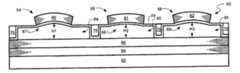
- FIG. 3therein is shown a cross-sectional view of a monolithic VCSEL array 60 of the present invention in one stage of manufacturing.
- the array 60includes a substrate 62 .
- a lower mirror or lower DBR 64which consists of a plurality of alternating high and low index of refraction materials.
- the lower DBR 64can be made from a number of different combinations of dielectric layers, such as SiO 2 , SiC, TiO 2 , and A 1203 , they can be semiconductor layers, or they could be combinations of semiconductors, dielectric materials, and metal.
- Each of the layersis ⁇ 1 ⁇ 4 of a wavelength ( ⁇ haeck over (S) ⁇ /4) in optical thickness and the layers are combined until the lower DBR 64 has an overall reflectance of almost 100%.
- the lower DBR 64is a photoactive semiconductor structure 66 , which contains quantum wells as previously described.
- the quantum wellmay be a single quantum well or multiple quantum wells with a number of alternating thin layers of high- and low-bandgap semiconductor materials.
- the photoactive semiconductor structure 66is made from multiple layers of materials such as those containing aluminum, indium, gallium, arsenic, nitrogen, and/or phosphorous.
- the photoactive semiconductor structure 66is a sacrificial layer, which has been formed into sacrificial islands 70 - 72 using standard lithography and etching processes.
- the sacrificial islands 70 - 72can have different shapes, but in one mode, they are disk-shaped and have different diameters to allow control of the optical characteristics of the final VCODs as will later be explained.
- the sacrificial islands 70 - 72are deposited on the photoactive semiconductor structure 66 and are of an etchable material, such as polyimide, which can readily be removed in an oxygen plasma. Alternately, they can be made of semiconductor layers that can be removed by selective etching.
- a reflector support 74is deposited on the photoactive semiconductor structure 66 and covers the sacrificial islands 70 - 72 .
- the reflector support 74can be made of a material such as silicon nitride, an organic polymer, or it can be a semiconductor material.
- An anchor 76is deposited on the reflector support 74 where it is attached to the photoactive semiconductor structure 66 .
- the anchor 76can be made with the same materials as the top DBRs 80 - 82 , it can be made of dielectrics such as SiO 2 or Si 3 N 4 , or it can be a metal such as gold or aluminum.
- the materials used to form the upper DBRs 80 - 82are deposited to cover the reflector support 74 and the anchor 76 . These layers are alternating layers of low and high index of refraction materials that will be etched to form the upper mirrors or upper DBRs 80 - 82 .
- the DBRs 80 - 82can be made from dielectric materials such as SiO 2 , SiC, TiO 2 , and Al 2 O 3 , or they can be semiconductor layers, or they could be combinations of semiconductors, dielectric materials, and metal. There are a number of ways to deposit these materials such as plasma deposition, evaporation, sputtering, ion assisted deposition, or epitaxial growth.
- the upper DBRs 80 - 82can have different shapes and sizes, but in the one preferred mode, they are disks having the same diameters centrally placed on portions of the reflector support 74 having different diameters.
- the upper DBR materials and the materials used for the reflector support 74will contain residual stresses, either tensile or compressive.
- the existence of the residual stresses in these layersis evident to those having ordinary skill in the art.
- the stressescan be tailored in a variety of ways during the deposition of the films. In plasma deposition, various factors such as gas flows, temperature, and pressure can be changed to affect the internal stress in the deposited material. In sputtering, for example, the temperature and the voltage of the sputtering, or in ion-assisted deposition, the ion energy, affect the stress. The importance of these residual stresses will become apparent to those skilled in the art from the following descriptions.
- FIG. 4therein is shown the cross-sectional view of the VCSEL array of FIG. 3 in one embodiment of the present invention.
- the same elements in FIG. 4have the same numbers as in FIG. 3 .
- the reflector support 74which in one mode forms a plurality of different size drum-shaped configurations based on the disk-shape of the sacrificial islands 70 - 72 , have been etched to form openings, such as sectors or holes, for removal of the sacrificial islands 70 - 72 by etching to create air gaps 84 - 86 .
- openingssuch as sectors or holes
- the bows 87 - 89 in the reflector support 74results in the air gaps 84 - 86 having different heights H1, H2, H3 at their centers due to the different diameters of the drum-shaped configurations.
- the heights H1, H2, H3 of the air gaps 84 - 86 , respectively, and the thicknesses of the photoactive semiconductor structure 66 and the reflector support 74define the optical heights of the resonant cavities of a plurality of VCODs 90 - 92 and, thus, the wavelengths of laser light they will emit when activated.
- the different heights H1, H2, H3can be obtained through photolithography using a single mask to control the geometrical size and/or shape of the anchors or of the upper DBRs 80 - 82 , or the geometrical size, shape, and/or configuration of the openings in the reflector support 74 .
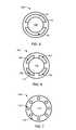
- FIG. 5therein is shown a plan view of one embodiment of a single portion of a reflector support 100 according to the present invention.
- the reflector support 100has two sector portions 101 and 102 removed to leave a single strap 103 supporting a reflector 104 .
- FIG. 6therein is shown a plan view of another embodiment of a single portion of a reflector support 105 according to the present invention.
- the reflector support 105has four sectors 106 - 109 removed so a double strap 110 supports a reflector 112 .
- FIG. 7therein is shown a plan view of a further embodiment of a single portion of a reflector support 114 according to the present invention.
- the reflector support 114has a plurality of openings 116 provided therein with the remaining portion 117 supporting a reflector 118 .
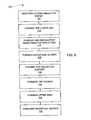
- a first step 122is providing the wafer 52 .
- a second step 124is forming the lower DBR 64 over the wafer 52 .
- a third step 126is forming the photoactive semiconductor structure 66 over the lower DBR 64 .
- a fourth step 128is forming first and second sacrificial islands 70 and 71 of a sacrificial layer over the photoactive semiconductor structure 66 with the first and second sacrificial islands 70 and 71 having respective first and second different sizes. If the first and second sacrificial islands 70 and 71 are disk-shaped, the first and second sacrificial islands 70 and 71 will have first and second diameters, which are different. Different size and shape sacrificial islands can be formed for the entire wafer 52 using a single mask.
- a fifth step 130involves forming the reflector support 74 over the first and second sacrificial islands 70 and 71 .
- the reflector support 74is conformally deposited over the first and second sacrificial islands 70 and 71 and is attached to the photoactive semiconductor structure 66 around the first and second sacrificial islands 70 and 71 . It will be noted that the first and second sacrificial islands 70 and 71 are far enough apart that there is space between the first and second sacrificial islands 70 and 71 even after the reflector support 74 has been deposited.
- the sixth step 132involves forming the anchor 76 between the first and second sacrificial islands 70 and 71 over the reflector support 74 . Different sizes and shapes for the anchor 74 over the reflector support 74 can be formed for the entire wafer 52 using a single mask.
- a seventh step 134involves forming first and second upper DBRs 80 and 81 over the reflector support 74 . This involves depositing a reflector layer and patterning and etching the reflector layer to form the first and second upper DBRs 80 and 81 . Different size and shape upper DBRs can be formed for the entire wafer 52 using a single mask.
- An eighth step 136involves removing the first and second sacrificial islands 70 and 71 to form first and second air gaps 84 and 85 .
- This stepsectors or openings are formed in the reflector support 74 and the first and second sacrificial islands 70 and 71 are etched away through the openings to form the first and second air gaps 84 and 85 .
- This removal stepcauses the first optical device 54 to be formed by the lower DBR 64 , the photoactive semiconductor structure 66 , the first air gap 84 , and the first upper DBR 80 .
- a second optical device 55is formed by the lower DBR 64 , the photoactive semiconductor structure 66 , the second air gap 85 , and the second upper DBR 81 .
- the first and second air gaps 84 and 85will be of different heights H1 and H2 due to: the stress imposed during the forming of the upper reflective layer; the geometrical size of the anchors 76 or of the first and second upper DBRs 80 and 81 ; or the geometrical size and configuration of the openings in the reflector support 74 .
- the different heights H1 and H2provide the first and second optical devices 54 and 55 with different emission wavelengths.
- the flow chart 120is merely exemplary and many other steps may be added and some removed as would be evident to those having ordinary skill in the art.
- the wafer 52can be sliced and packaged.
Landscapes
- Physics & Mathematics (AREA)
- Condensed Matter Physics & Semiconductors (AREA)
- General Physics & Mathematics (AREA)
- Electromagnetism (AREA)
- Optics & Photonics (AREA)
- Semiconductor Lasers (AREA)
Abstract
Description
Claims (10)
Priority Applications (4)
| Application Number | Priority Date | Filing Date | Title |
|---|---|---|---|
| US10/151,646US6806110B2 (en) | 2002-05-16 | 2002-05-16 | Monolithic multi-wavelength vertical-cavity surface emitting laser array and method of manufacture therefor |
| EP03002337AEP1363369B1 (en) | 2002-05-16 | 2003-02-03 | Monolithic multi-wavelength vertical-cavity surface emitting laser array and method of manufacture therefor |
| DE60304931TDE60304931T2 (en) | 2002-05-16 | 2003-02-03 | Multi-wavelength monolithic array of vertical cavity surface emitting lasers and method of fabrication thereof |
| JP2003126147AJP2003332686A (en) | 2002-05-16 | 2003-05-01 | Method of manufacturing a monolithic array of vertical cavity optical devices |
Applications Claiming Priority (1)
| Application Number | Priority Date | Filing Date | Title |
|---|---|---|---|
| US10/151,646US6806110B2 (en) | 2002-05-16 | 2002-05-16 | Monolithic multi-wavelength vertical-cavity surface emitting laser array and method of manufacture therefor |
Publications (2)
| Publication Number | Publication Date |
|---|---|
| US20030214992A1 US20030214992A1 (en) | 2003-11-20 |
| US6806110B2true US6806110B2 (en) | 2004-10-19 |
Family
ID=29269815
Family Applications (1)
| Application Number | Title | Priority Date | Filing Date |
|---|---|---|---|
| US10/151,646Expired - Fee RelatedUS6806110B2 (en) | 2002-05-16 | 2002-05-16 | Monolithic multi-wavelength vertical-cavity surface emitting laser array and method of manufacture therefor |
Country Status (4)
| Country | Link |
|---|---|
| US (1) | US6806110B2 (en) |
| EP (1) | EP1363369B1 (en) |
| JP (1) | JP2003332686A (en) |
| DE (1) | DE60304931T2 (en) |
Cited By (26)
| Publication number | Priority date | Publication date | Assignee | Title |
|---|---|---|---|---|
| US20060294025A1 (en)* | 2005-06-28 | 2006-12-28 | Paypal Inc. | Mobile device communication system |
| US7492502B2 (en) | 2004-09-27 | 2009-02-17 | Idc, Llc | Method of fabricating a free-standing microstructure |
| US7527996B2 (en) | 2006-04-19 | 2009-05-05 | Qualcomm Mems Technologies, Inc. | Non-planar surface structures and process for microelectromechanical systems |
| US7534640B2 (en) | 2005-07-22 | 2009-05-19 | Qualcomm Mems Technologies, Inc. | Support structure for MEMS device and methods therefor |
| US7547565B2 (en)* | 2005-02-04 | 2009-06-16 | Qualcomm Mems Technologies, Inc. | Method of manufacturing optical interference color display |
| US7547568B2 (en) | 2006-02-22 | 2009-06-16 | Qualcomm Mems Technologies, Inc. | Electrical conditioning of MEMS device and insulating layer thereof |
| US7556917B2 (en) | 2003-04-15 | 2009-07-07 | Idc, Llc | Method for manufacturing an array of interferometric modulators |
| US7561321B2 (en) | 2006-06-01 | 2009-07-14 | Qualcomm Mems Technologies, Inc. | Process and structure for fabrication of MEMS device having isolated edge posts |
| US7569488B2 (en) | 2007-06-22 | 2009-08-04 | Qualcomm Mems Technologies, Inc. | Methods of making a MEMS device by monitoring a process parameter |
| US7616369B2 (en) | 2003-06-24 | 2009-11-10 | Idc, Llc | Film stack for manufacturing micro-electromechanical systems (MEMS) devices |
| US7623287B2 (en) | 2006-04-19 | 2009-11-24 | Qualcomm Mems Technologies, Inc. | Non-planar surface structures and process for microelectromechanical systems |
| US7706044B2 (en) | 2003-05-26 | 2010-04-27 | Qualcomm Mems Technologies, Inc. | Optical interference display cell and method of making the same |
| US7719752B2 (en) | 2007-05-11 | 2010-05-18 | Qualcomm Mems Technologies, Inc. | MEMS structures, methods of fabricating MEMS components on separate substrates and assembly of same |
| US7733552B2 (en) | 2007-03-21 | 2010-06-08 | Qualcomm Mems Technologies, Inc | MEMS cavity-coating layers and methods |
| US7763546B2 (en) | 2006-08-02 | 2010-07-27 | Qualcomm Mems Technologies, Inc. | Methods for reducing surface charges during the manufacture of microelectromechanical systems devices |
| US7795061B2 (en) | 2005-12-29 | 2010-09-14 | Qualcomm Mems Technologies, Inc. | Method of creating MEMS device cavities by a non-etching process |
| US7835093B2 (en) | 2005-08-19 | 2010-11-16 | Qualcomm Mems Technologies, Inc. | Methods for forming layers within a MEMS device using liftoff processes |
| US7864403B2 (en) | 2009-03-27 | 2011-01-04 | Qualcomm Mems Technologies, Inc. | Post-release adjustment of interferometric modulator reflectivity |
| US7952789B2 (en) | 2006-03-02 | 2011-05-31 | Qualcomm Mems Technologies, Inc. | MEMS devices with multi-component sacrificial layers |
| US8064124B2 (en) | 2006-01-18 | 2011-11-22 | Qualcomm Mems Technologies, Inc. | Silicon-rich silicon nitrides as etch stops in MEMS manufacture |
| US8115988B2 (en) | 2004-07-29 | 2012-02-14 | Qualcomm Mems Technologies, Inc. | System and method for micro-electromechanical operation of an interferometric modulator |
| US8149497B2 (en) | 2005-07-22 | 2012-04-03 | Qualcomm Mems Technologies, Inc. | Support structure for MEMS device and methods therefor |
| US8278726B2 (en) | 2002-09-20 | 2012-10-02 | Qualcomm Mems Technologies, Inc. | Controlling electromechanical behavior of structures within a microelectromechanical systems device |
| US8358458B2 (en) | 2008-06-05 | 2013-01-22 | Qualcomm Mems Technologies, Inc. | Low temperature amorphous silicon sacrificial layer for controlled adhesion in MEMS devices |
| US8368124B2 (en) | 2002-09-20 | 2013-02-05 | Qualcomm Mems Technologies, Inc. | Electromechanical devices having etch barrier layers |
| US8659816B2 (en) | 2011-04-25 | 2014-02-25 | Qualcomm Mems Technologies, Inc. | Mechanical layer and methods of making the same |
Families Citing this family (11)
| Publication number | Priority date | Publication date | Assignee | Title |
|---|---|---|---|---|
| US7039075B2 (en)* | 2003-04-11 | 2006-05-02 | Thornton Robert L | Fiber extended, semiconductor laser |
| DE102004052686A1 (en)* | 2004-08-23 | 2006-03-02 | Osram Opto Semiconductors Gmbh | Semiconductor element as for a laser such as a vertical external cavity surface emitting laser has curved mirror integrated into a monolithic semiconductor body |
| JP2009272375A (en)* | 2008-05-01 | 2009-11-19 | Sumitomo Electric Ind Ltd | Method of manufacturing semiconductor laser, and semiconductor laser |
| CN102714396B (en)* | 2010-01-29 | 2014-12-10 | 惠普发展公司,有限责任合伙企业 | Multimode Vertical Cavity Surface Emitting Laser Array |
| US9112331B2 (en) | 2012-03-22 | 2015-08-18 | Palo Alto Research Center Incorporated | Surface emitting laser incorporating third reflector |
| US9124062B2 (en)* | 2012-03-22 | 2015-09-01 | Palo Alto Research Center Incorporated | Optically pumped surface emitting lasers incorporating high reflectivity/bandwidth limited reflector |
| US9112332B2 (en) | 2012-06-14 | 2015-08-18 | Palo Alto Research Center Incorporated | Electron beam pumped vertical cavity surface emitting laser |
| JP5969677B2 (en)* | 2015-10-05 | 2016-08-17 | ヒューレット−パッカード デベロップメント カンパニー エル.ピー.Hewlett‐Packard Development Company, L.P. | Multimode monolithic vertical cavity surface emitting laser array and laser system using the same |
| CN107565380B (en)* | 2017-08-29 | 2019-04-16 | 中国航空工业集团公司洛阳电光设备研究所 | A kind of multi-wave length laser device of coaxial output |
| WO2021140803A1 (en)* | 2020-01-08 | 2021-07-15 | ソニーグループ株式会社 | Light emitting element |
| JP2024110811A (en)* | 2023-02-03 | 2024-08-16 | キヤノン株式会社 | antenna |
Citations (9)
| Publication number | Priority date | Publication date | Assignee | Title |
|---|---|---|---|---|
| US5291502A (en) | 1992-09-04 | 1994-03-01 | The Board Of Trustees Of The Leland Stanford, Jr. University | Electrostatically tunable optical device and optical interconnect for processors |
| US5739945A (en) | 1995-09-29 | 1998-04-14 | Tayebati; Parviz | Electrically tunable optical filter utilizing a deformable multi-layer mirror |
| WO1999034484A2 (en) | 1997-12-29 | 1999-07-08 | Coretek, Inc. | Microelectromechanically, tunable, confocal, vcsel and fabry-perot filter |
| US5991326A (en)* | 1998-04-14 | 1999-11-23 | Bandwidth9, Inc. | Lattice-relaxed verticle optical cavities |
| US6324192B1 (en)* | 1995-09-29 | 2001-11-27 | Coretek, Inc. | Electrically tunable fabry-perot structure utilizing a deformable multi-layer mirror and method of making the same |
| US6341137B1 (en) | 1999-04-27 | 2002-01-22 | Gore Enterprise Holdings, Inc. | Wavelength division multiplexed array of long-wavelength vertical cavity lasers |
| US20020131464A1 (en)* | 2001-03-15 | 2002-09-19 | Ecole Polytechnique Federale De Lausanne | Vertical cavity surface emitting laser and a method of fabrication thereof |
| US20030033122A1 (en)* | 2001-03-15 | 2003-02-13 | Dempsey Derek M. | Performance assessment of data classifiers |
| US20030039284A1 (en)* | 2001-08-16 | 2003-02-27 | Jun Zheng | VCSEL with heat-spreading layer |
- 2002
- 2002-05-16USUS10/151,646patent/US6806110B2/ennot_activeExpired - Fee Related
- 2003
- 2003-02-03EPEP03002337Apatent/EP1363369B1/ennot_activeExpired - Lifetime
- 2003-02-03DEDE60304931Tpatent/DE60304931T2/ennot_activeExpired - Fee Related
- 2003-05-01JPJP2003126147Apatent/JP2003332686A/ennot_activeWithdrawn
Patent Citations (9)
| Publication number | Priority date | Publication date | Assignee | Title |
|---|---|---|---|---|
| US5291502A (en) | 1992-09-04 | 1994-03-01 | The Board Of Trustees Of The Leland Stanford, Jr. University | Electrostatically tunable optical device and optical interconnect for processors |
| US5739945A (en) | 1995-09-29 | 1998-04-14 | Tayebati; Parviz | Electrically tunable optical filter utilizing a deformable multi-layer mirror |
| US6324192B1 (en)* | 1995-09-29 | 2001-11-27 | Coretek, Inc. | Electrically tunable fabry-perot structure utilizing a deformable multi-layer mirror and method of making the same |
| WO1999034484A2 (en) | 1997-12-29 | 1999-07-08 | Coretek, Inc. | Microelectromechanically, tunable, confocal, vcsel and fabry-perot filter |
| US5991326A (en)* | 1998-04-14 | 1999-11-23 | Bandwidth9, Inc. | Lattice-relaxed verticle optical cavities |
| US6341137B1 (en) | 1999-04-27 | 2002-01-22 | Gore Enterprise Holdings, Inc. | Wavelength division multiplexed array of long-wavelength vertical cavity lasers |
| US20020131464A1 (en)* | 2001-03-15 | 2002-09-19 | Ecole Polytechnique Federale De Lausanne | Vertical cavity surface emitting laser and a method of fabrication thereof |
| US20030033122A1 (en)* | 2001-03-15 | 2003-02-13 | Dempsey Derek M. | Performance assessment of data classifiers |
| US20030039284A1 (en)* | 2001-08-16 | 2003-02-27 | Jun Zheng | VCSEL with heat-spreading layer |
Non-Patent Citations (5)
| Title |
|---|
| Eng, L.E. et al., "Wavelength Shift in Vertical Cavity Laser Arrays on a Patterned Substrates", Electronics Letters, No. 31, No. 7, Mar. 30, 1995, pp. 562-563. |
| Huffaker, D.L. et al., "Multiwavelength, Densely-Packed 2 x 2 Vertical-Cavity Surface_Emitting Laser Array Fabricated Using Selective Oxidation", IEEE Photonics Technology Letters, vol. 8, No. 7, Jul. 1, 1996, pp. 858-860. |
| Koyama, F. et al., "Two-Dimensional Multiwavelength Surface Emitting Laser Arrays Fabricated by Nonplanar MOCVD", Electronics Letters, vol. 30, No. 23, Nov. 10, 1994, pp. 1947-1948. |
| Mauro J. Kobrinsky, Erik R. Deutsch, and Stephen D. Senturia, "Effect of Support Compliance and Residual Stress on the shape ofb Doubly Supported Surface-Micromachined Beams", Journal of Microelectromechnical Systems, vol. 9, No. 3, pp. 361-369, Sep. 2000. |
| Seassal, C. et al., "Micromachined Structures for Vertical Microelectrooptical Device on InP", Indium Phosphide and Related Materials, Apr. 21-25, 1996, pp. 275-278. |
Cited By (34)
| Publication number | Priority date | Publication date | Assignee | Title |
|---|---|---|---|---|
| US8368124B2 (en) | 2002-09-20 | 2013-02-05 | Qualcomm Mems Technologies, Inc. | Electromechanical devices having etch barrier layers |
| US8278726B2 (en) | 2002-09-20 | 2012-10-02 | Qualcomm Mems Technologies, Inc. | Controlling electromechanical behavior of structures within a microelectromechanical systems device |
| US7556917B2 (en) | 2003-04-15 | 2009-07-07 | Idc, Llc | Method for manufacturing an array of interferometric modulators |
| US7723015B2 (en) | 2003-04-15 | 2010-05-25 | Qualcomm Mems Technologies, Inc. | Method for manufacturing an array of interferometeric modulators |
| US7706044B2 (en) | 2003-05-26 | 2010-04-27 | Qualcomm Mems Technologies, Inc. | Optical interference display cell and method of making the same |
| US7616369B2 (en) | 2003-06-24 | 2009-11-10 | Idc, Llc | Film stack for manufacturing micro-electromechanical systems (MEMS) devices |
| US8115988B2 (en) | 2004-07-29 | 2012-02-14 | Qualcomm Mems Technologies, Inc. | System and method for micro-electromechanical operation of an interferometric modulator |
| US7492502B2 (en) | 2004-09-27 | 2009-02-17 | Idc, Llc | Method of fabricating a free-standing microstructure |
| US7547565B2 (en)* | 2005-02-04 | 2009-06-16 | Qualcomm Mems Technologies, Inc. | Method of manufacturing optical interference color display |
| US20060294025A1 (en)* | 2005-06-28 | 2006-12-28 | Paypal Inc. | Mobile device communication system |
| US7831520B2 (en) | 2005-06-28 | 2010-11-09 | Ebay Inc. | Mobile device communication system |
| US7534640B2 (en) | 2005-07-22 | 2009-05-19 | Qualcomm Mems Technologies, Inc. | Support structure for MEMS device and methods therefor |
| US8149497B2 (en) | 2005-07-22 | 2012-04-03 | Qualcomm Mems Technologies, Inc. | Support structure for MEMS device and methods therefor |
| US8218229B2 (en) | 2005-07-22 | 2012-07-10 | Qualcomm Mems Technologies, Inc. | Support structure for MEMS device and methods therefor |
| US8298847B2 (en) | 2005-08-19 | 2012-10-30 | Qualcomm Mems Technologies, Inc. | MEMS devices having support structures with substantially vertical sidewalls and methods for fabricating the same |
| US7835093B2 (en) | 2005-08-19 | 2010-11-16 | Qualcomm Mems Technologies, Inc. | Methods for forming layers within a MEMS device using liftoff processes |
| US8394656B2 (en) | 2005-12-29 | 2013-03-12 | Qualcomm Mems Technologies, Inc. | Method of creating MEMS device cavities by a non-etching process |
| US7795061B2 (en) | 2005-12-29 | 2010-09-14 | Qualcomm Mems Technologies, Inc. | Method of creating MEMS device cavities by a non-etching process |
| US8064124B2 (en) | 2006-01-18 | 2011-11-22 | Qualcomm Mems Technologies, Inc. | Silicon-rich silicon nitrides as etch stops in MEMS manufacture |
| US7547568B2 (en) | 2006-02-22 | 2009-06-16 | Qualcomm Mems Technologies, Inc. | Electrical conditioning of MEMS device and insulating layer thereof |
| US7952789B2 (en) | 2006-03-02 | 2011-05-31 | Qualcomm Mems Technologies, Inc. | MEMS devices with multi-component sacrificial layers |
| US7623287B2 (en) | 2006-04-19 | 2009-11-24 | Qualcomm Mems Technologies, Inc. | Non-planar surface structures and process for microelectromechanical systems |
| US7527996B2 (en) | 2006-04-19 | 2009-05-05 | Qualcomm Mems Technologies, Inc. | Non-planar surface structures and process for microelectromechanical systems |
| US7561321B2 (en) | 2006-06-01 | 2009-07-14 | Qualcomm Mems Technologies, Inc. | Process and structure for fabrication of MEMS device having isolated edge posts |
| US7763546B2 (en) | 2006-08-02 | 2010-07-27 | Qualcomm Mems Technologies, Inc. | Methods for reducing surface charges during the manufacture of microelectromechanical systems devices |
| US8164815B2 (en) | 2007-03-21 | 2012-04-24 | Qualcomm Mems Technologies, Inc. | MEMS cavity-coating layers and methods |
| US7733552B2 (en) | 2007-03-21 | 2010-06-08 | Qualcomm Mems Technologies, Inc | MEMS cavity-coating layers and methods |
| US8284475B2 (en) | 2007-05-11 | 2012-10-09 | Qualcomm Mems Technologies, Inc. | Methods of fabricating MEMS with spacers between plates and devices formed by same |
| US7719752B2 (en) | 2007-05-11 | 2010-05-18 | Qualcomm Mems Technologies, Inc. | MEMS structures, methods of fabricating MEMS components on separate substrates and assembly of same |
| US8830557B2 (en) | 2007-05-11 | 2014-09-09 | Qualcomm Mems Technologies, Inc. | Methods of fabricating MEMS with spacers between plates and devices formed by same |
| US7569488B2 (en) | 2007-06-22 | 2009-08-04 | Qualcomm Mems Technologies, Inc. | Methods of making a MEMS device by monitoring a process parameter |
| US8358458B2 (en) | 2008-06-05 | 2013-01-22 | Qualcomm Mems Technologies, Inc. | Low temperature amorphous silicon sacrificial layer for controlled adhesion in MEMS devices |
| US7864403B2 (en) | 2009-03-27 | 2011-01-04 | Qualcomm Mems Technologies, Inc. | Post-release adjustment of interferometric modulator reflectivity |
| US8659816B2 (en) | 2011-04-25 | 2014-02-25 | Qualcomm Mems Technologies, Inc. | Mechanical layer and methods of making the same |
Also Published As
| Publication number | Publication date |
|---|---|
| DE60304931T2 (en) | 2007-01-04 |
| EP1363369A1 (en) | 2003-11-19 |
| JP2003332686A (en) | 2003-11-21 |
| DE60304931D1 (en) | 2006-06-08 |
| US20030214992A1 (en) | 2003-11-20 |
| EP1363369B1 (en) | 2006-05-03 |
Similar Documents
| Publication | Publication Date | Title |
|---|---|---|
| US6806110B2 (en) | Monolithic multi-wavelength vertical-cavity surface emitting laser array and method of manufacture therefor | |
| EP1363370B1 (en) | Fixed wavelength vertical cavity optical devices and method of manufacture thereof | |
| US6117699A (en) | Monolithic multiple wavelength VCSEL array | |
| EP1030420B1 (en) | A vertical cavity surface emitting laser array and a process for making same | |
| TWI429152B (en) | Vertical-cavity surface-emitting laser system and method for fabricating the same | |
| US20030031221A1 (en) | Single mode operation of microelectromechanically tunable, half-symmetric, vertical cavity surface emitting lasers | |
| EP1182758B1 (en) | Multi-wavelength surface emitting laser and method for manufacturing the same | |
| CN1285034A (en) | Microelectromechanically, tunable, confocel, VCSEL and fabry-perot filter | |
| AU2784799A (en) | Vertical optical cavities produced with selective area epitaxy | |
| US20050169343A1 (en) | Polarization control of vertical diode lasers by monolithically integrated surface grating | |
| WO2001093385A2 (en) | Surface-emitting laser devices with integrated beam-shaping optics and power-monitoring detectors | |
| US6696307B2 (en) | Patterned phase shift layers for wavelength-selectable vertical cavity surface-emitting laser (VCSEL) arrays | |
| JP4360806B2 (en) | Optically pumped surface emitting semiconductor laser device and method for manufacturing the same | |
| US6693934B2 (en) | Wavelength division multiplexed vertical cavity surface emitting laser array | |
| US6628685B1 (en) | Method of fabricating long-wavelength VCSEL and apparatus | |
| US5029176A (en) | Monolithic multiple-wavelength laser array | |
| US6724796B2 (en) | Modified distributed bragg reflector (DBR) for vertical cavity surface-emitting laser (VCSEL) resonant wavelength tuning sensitivity control | |
| US7116483B2 (en) | Distributed bragg reflector and method of fabrication | |
| EP2033281B1 (en) | A method for fabricating a photonic crystal or photonic bandgap vertical-cavity surface-emitting laser | |
| US6061485A (en) | Method for wavelength division multiplexing utilizing donut mode vertical cavity surface emitting lasers | |
| JPH10233559A (en) | Semiconductor laser device, manufacturing method thereof, and optical communication system using the same | |
| WO2002089276A1 (en) | Surface emitting laser | |
| KR100460839B1 (en) | Multiple wavelength and long-wavelength vertical cavity surface emitting laser array and fabricating method the same | |
| JP2000294873A (en) | Surface emitting type laser array and manufacture of the same | |
| JP3944677B2 (en) | Manufacturing method of surface emitting semiconductor laser |
Legal Events
| Date | Code | Title | Description |
|---|---|---|---|
| AS | Assignment | Owner name:AGILENT TECHNOLOGIES, INC., COLORADO Free format text:ASSIGNMENT OF ASSIGNORS INTEREST;ASSIGNORS:LESTER, STEVEN D.;ROBBINS, VIRGINIA M.;MILLER, JEFFREY N.;REEL/FRAME:013093/0509;SIGNING DATES FROM 20020513 TO 20020514 | |
| AS | Assignment | Owner name:AVAGO TECHNOLOGIES GENERAL IP PTE. LTD., SINGAPORE Free format text:ASSIGNMENT OF ASSIGNORS INTEREST;ASSIGNOR:AGILENT TECHNOLOGIES, INC.;REEL/FRAME:017207/0020 Effective date:20051201 | |
| AS | Assignment | Owner name:AVAGO TECHNOLOGIES FIBER IP (SINGAPORE) PTE. LTD., Free format text:ASSIGNMENT OF ASSIGNORS INTEREST;ASSIGNOR:AVAGO TECHNOLOGIES GENERAL IP (SINGAPORE) PTE. LTD.;REEL/FRAME:017675/0199 Effective date:20060127 | |
| FPAY | Fee payment | Year of fee payment:4 | |
| FPAY | Fee payment | Year of fee payment:8 | |
| AS | Assignment | Owner name:AVAGO TECHNOLOGIES GENERAL IP (SINGAPORE) PTE. LTD Free format text:MERGER;ASSIGNOR:AVAGO TECHNOLOGIES FIBER IP (SINGAPORE) PTE. LTD.;REEL/FRAME:030369/0672 Effective date:20121030 | |
| AS | Assignment | Owner name:AVAGO TECHNOLOGIES GENERAL IP (SINGAPORE) PTE. LTD Free format text:CORRECTIVE ASSIGNMENT TO CORRECT THE NAME OF THE ASSIGNEE PREVIOUSLY RECORDED ON REEL 017207 FRAME 0020. ASSIGNOR(S) HEREBY CONFIRMS THE ASSIGNMENT;ASSIGNOR:AGILENT TECHNOLOGIES, INC.;REEL/FRAME:038633/0001 Effective date:20051201 | |
| REMI | Maintenance fee reminder mailed | ||
| LAPS | Lapse for failure to pay maintenance fees | ||
| STCH | Information on status: patent discontinuation | Free format text:PATENT EXPIRED DUE TO NONPAYMENT OF MAINTENANCE FEES UNDER 37 CFR 1.362 | |
| FP | Expired due to failure to pay maintenance fee | Effective date:20161019 |