US6805054B1 - Method, system and holder for transferring templates during imprint lithography processes - Google Patents
Method, system and holder for transferring templates during imprint lithography processesDownload PDFInfo
- Publication number
- US6805054B1 US6805054B1US10/438,224US43822403AUS6805054B1US 6805054 B1US6805054 B1US 6805054B1US 43822403 AUS43822403 AUS 43822403AUS 6805054 B1US6805054 B1US 6805054B1
- Authority
- US
- United States
- Prior art keywords
- template
- holder
- imprint
- imprint head
- support members
- Prior art date
- Legal status (The legal status is an assumption and is not a legal conclusion. Google has not performed a legal analysis and makes no representation as to the accuracy of the status listed.)
- Expired - Lifetime, expires
Links
Images


Classifications
- G—PHYSICS
- G03—PHOTOGRAPHY; CINEMATOGRAPHY; ANALOGOUS TECHNIQUES USING WAVES OTHER THAN OPTICAL WAVES; ELECTROGRAPHY; HOLOGRAPHY
- G03F—PHOTOMECHANICAL PRODUCTION OF TEXTURED OR PATTERNED SURFACES, e.g. FOR PRINTING, FOR PROCESSING OF SEMICONDUCTOR DEVICES; MATERIALS THEREFOR; ORIGINALS THEREFOR; APPARATUS SPECIALLY ADAPTED THEREFOR
- G03F7/00—Photomechanical, e.g. photolithographic, production of textured or patterned surfaces, e.g. printing surfaces; Materials therefor, e.g. comprising photoresists; Apparatus specially adapted therefor
- G03F7/0002—Lithographic processes using patterning methods other than those involving the exposure to radiation, e.g. by stamping
- B—PERFORMING OPERATIONS; TRANSPORTING
- B82—NANOTECHNOLOGY
- B82Y—SPECIFIC USES OR APPLICATIONS OF NANOSTRUCTURES; MEASUREMENT OR ANALYSIS OF NANOSTRUCTURES; MANUFACTURE OR TREATMENT OF NANOSTRUCTURES
- B82Y10/00—Nanotechnology for information processing, storage or transmission, e.g. quantum computing or single electron logic
- B—PERFORMING OPERATIONS; TRANSPORTING
- B82—NANOTECHNOLOGY
- B82Y—SPECIFIC USES OR APPLICATIONS OF NANOSTRUCTURES; MEASUREMENT OR ANALYSIS OF NANOSTRUCTURES; MANUFACTURE OR TREATMENT OF NANOSTRUCTURES
- B82Y40/00—Manufacture or treatment of nanostructures
Definitions
- the present inventionrelates generally to imprint lithography. More particularly, the present invention is directed to a method, system and holder to transfer templates during imprint lithography processes.
- Micro-fabrication techniquescan produce structures having features on the order of nanometers. Micro-fabrication is used in a wide variety of applications, such as the manufacturing of integrated circuits (i.e. semiconductor processing), biotechnology, optical technology, mechanical systems, and micro-electro-mechanical systems (“MEMS”).
- integrated circuitsi.e. semiconductor processing
- biotechnologyi.e., biotechnology
- optical technologyi.e., optical technology
- mechanical systemsi.e. optical technology
- MEMSmicro-electro-mechanical systems
- Imprint lithographyis a type of micro-fabrication technique that is becoming increasingly important in semiconductor processing and other applications. Imprint lithography provides greater process control and reduction of the minimum feature dimension of the structures formed. This in turn provides higher production yields and more integrated circuits per wafer, for example.
- Micro-fabricationcan be used to form a relief image on a substrate, such as a semiconductor wafer.
- the substratetypically has a transfer layer that is coated with a thin layer of polymerizable fluid, thermoplastic, or other imprint material capable of being formed (i.e. molded or imprinted) into a desired structure.
- a mold with a relief structuremakes mechanical contact with the substrate and the polymerizable fluid or other imprint material fills the relief structure of the mold.
- the polymerizable fluidis then polymerized to form the desired structure on the transfer layer, which is complimentary to the relief structure of the mold.
- the transfer layer and the solidified polymeric materialcan then be etched to form a relief image in the transfer layer, or coated with a thin-film layer of other material, for example.
- Imprint lithography systemsoften use an imprint head with a mold, also called a template, which can be installed and removed from the imprint head. This allows the imprint lithography system to be used to imprint different patterns. In this manner, the imprint lithography system can be used to fabricate various types of circuits or other devices, or imprint various structures on a substrate.
- a moldalso called a template
- a method for handling a template, having a patterned mold thereon, in an imprint lithography system having a motion stage with a chucking device coupled theretoincludes providing the template into a template transfer holder.
- the template transfer holderincludes a side coupled to the motion stage and support members extending from the side.
- the templateis disposed within the template transfer holder so as to have the patterned mold facing the side and spaced-apart therefrom. Relative movement is created between the motion stage and an imprint head to place the template transfer holder and the imprint head in superimposition.
- the templateis removed from the template transfer holder and suspended above the wafer chuck by the imprint head.
- a system and a template holderare described that facilitate the method.
- FIG. 1is a perspective view of an imprint lithography system for practicing embodiments of the present invention
- FIG. 2is a simplified side view of the imprint lithography system, shown in FIG. 1, demonstrating the spatial relationship between the mold and the wafer having imprinting material disposed thereon;
- FIG. 3is a simplified side view of the mold of FIG. 2 in contact with the imprinting layer
- FIG. 4is a simplified side view of an imprinting layer, shown in FIG. 2, patterned according to the template;
- FIG. 5is a simplified side view of the lithographic system, shown in FIG. 1, with a template transfer holder in a motion stage according to an embodiment of the present invention
- FIG. 6is a simplified side view of the template transfer holder of FIG. 5 in position to load the template in an imprint head;
- FIG. 7is a perspective view showing a template transfer holder of the template transfer system, shown in FIGS. 1, 5 and 6 , in accordance with one embodiment of the present invention.
- FIG. 8is a cross-sectional view of the template transfer holder, shown in FIG. 7, taken along lines 8 — 8 ;
- FIG. 9is a cross-sectional view of the template transfer holder, shown in FIG. 7, taken along lines 9 — 9 , and having a template disposed therein;
- FIG. 10is a simplified side view of the template transfer holder, shown in FIG. 7, taken along lines 10 — 10 ;
- FIG. 11is a simplified side view of the template transfer holder on a transfer substrate, shown in FIG. 5, according to another embodiment of the present invention.
- FIG. 12is a simplified side view of a template transfer holder on a transfer substrate above the wafer chuck, shown in FIG. 5, according to another embodiment of the present invention.
- FIG. 13is a simplified cross section of a template transfer assembly that may be employed in the lithographic system, shown in FIGS. 1 and 5, having a template coupled to a template transfer substrate with imprint material according to an embodiment of the present invention
- FIG. 14is a simplified cross section of a template transfer assembly, shown in FIG. 13, with a template coupled to a template transfer substrate with a perimeter of imprint material according to an alternate embodiment of the present invention
- FIG. 15is a simplified cross section of a template transfer assembly, shown in FIG. 13, with a template coupled to a template transfer substrate with a perimeter of imprint material according to a second embodiment of the present invention
- FIG. 16is a simplified cross section of a template transfer assembly, shown in FIG. 13, with a template coupled to a template transfer substrate with a perimeter of imprint material according to a third alternate embodiment of the present invention
- FIG. 17is a simplified flow chart of a method of handling a template in a lithographic system, shown in FIGS. 1, 2 , 3 , 4 , 5 , 11 , 12 , 13 , 14 , 15 and 16 , according to an embodiment of the present invention
- FIG. 18is a simplified flow chart of a method of removing a template from an imprint head of a lithographic imprinting system, shown in FIG. 17, according to another embodiment of the present invention.
- FIG. 19is a simplified flow chart of a method of installing a template from a template transfer substrate into an imprint head of a lithographic imprinting system, shown in FIG. 17, according to yet another embodiment of the present invention.
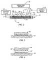
- FIG. 1is a perspective view of an imprint lithography system 10 for practicing embodiments of the present invention.
- a pair of spaced-apart bridge supports 12having a bridge 14 and a stage support 16 extending therebetween.
- Bridge 14 and stage support 16are spaced-apart.
- Coupled to bridge 14is an imprint head 18 that extends from bridge 14 toward stage support 16 and may move along and/or rotate about, X, Y and/or Z axes.
- a motion stage 20 and a template transfer system 40Disposed upon stage support 16 to face imprint head 18 .
- Motion stage 20is configured to move with respect to stage support 16 along one or more degrees of freedom. For example, motion stage 20 may move along and/or rotate about, X, Y and/or Z axes.
- motion stage 20holds a wafer 30 on a wafer chuck 21 , which is typically a vacuum chuck, and moves wafer 30 along the X and Y axes.
- a radiation source 22is coupled to imprint lithography system 10 to impinge actinic radiation upon motion stage 20 .
- Radiation source 22is coupled to bridge 14 and includes a power generator 23 connected to radiation source 22 .
- a template 26is removably connected to imprint head 18 .
- Template 26has first and second sides 26 a and 26 b .
- First side 26 afaces imprint head 18
- second side 26 bhas a mold 28 thereon facing away from imprint head 18 toward wafer chuck 21 .
- Mold 28generally includes a plurality of features defined by a plurality of spaced-apart recessions 28 a and protrusions 28 b , having a step height, h, on the order of nanometers (e.g. 100 nanometers).
- the plurality of featuresdefines an original pattern that is to be transferred onto a wafer 30 positioned on motion stage 20 .
- a distance, d, between mold 28 and a surface 32 of wafer 30may be varied.
- surface 32may comprise of material from which wafer 30 is formed, including any native oxide formed thereon and/or one or more layers of material deposited on wafer 30 .
- Imprinting layer 34is disposed on wafer 30 .
- Imprinting layer 34is generally a selected volume of imprint material, such as polymerizable fluid, applied to wafer 30 , either as a plurality of spaced-apart beads 36 , as shown, or in a continuous film.
- Exemplary imprint materialis described in U.S. patent application Ser. No. 10/178,947, filed Jun. 24, 2002 and entitled “Low Viscosity High Resolution Patterning Material”, which is incorporated by reference herein in its entirety.
- An exemplary method and system for depositing the imprint materialis disclosed in U.S. patent application Ser. No. 10/191,749, filed Jul. 2, 2002 and entitled “System and Method for Dispensing Liquids”, which is incorporated by reference herein in its entirety.
- Imprinting layer 34is generally flowable when mold 28 is brought into contact with imprinting layer 34 by creating relative movement between the imprint head 18 , shown in FIG. 1, and wafer 30 along the Z axis. In the present example, the relative movement is achieved by moving imprint head 318 along the Z axis.
- the imprint materialflows to form a contiguous layer that fills mold 28 .
- the imprint materialis then converted to a non-flowable (i.e. solid) state, such as by polymerization with actinic radiation, in the case of a polymerizable fluid imprint material, or by cooling, in the case of a thermoplastic imprint material.
- FIG. 4is a simplified side view of imprinting layer 34 ′ patterned according to mold 28 .
- Mold 28has been removed from imprinting layer 34 ′ by moving the imprint head 18 , shown in FIG. 1, away from wafer 30 .
- a structure 28 ′ recorded in imprinting layer 34 ′is produced, in part, by mechanical contact with mold 28 , and is generally an image of mold 28 . Wafer 30 with structure 28 ′ may then be further processed.
- Mold 28has features sized according to the structure 28 ′ desired to be imprinted to imprinting layer 34 ′, which can be on the order of nanometers. It is important to protect mold 28 from physical damage and/or contamination so that the desired structure 28 ′ is obtained when imprinting substrates.
- Template 26is removable from imprint head 18 of imprint lithography system 10 , shown in FIG. 1 . Another template can then be installed in imprint head 18 . For example, if template 26 wears out or is damaged, a replacement template may be installed, or a template with a different mold (i.e. structure or pattern) may be installed to imprint a different structure.
- Template 26is removably secured to imprint head 18 with vacuum and/or mechanical means, such as pins or clips. Mechanical means are desirable to ensure retention of template 26 in imprint head 18 in the event of a vacuum failure or in the event that vacuum is turned off during processing. Mechanical means of securing template 26 in imprint head 18 may also be convenient when installing or removing template 26 .
- the template 26is typically stored on template transfer system 40 so that first side 26 a faces imprint head 18 .
- template 26 and imprint head 18are placed in very close proximity (e.g. 10's of microns or less) to one another so that the template 26 can be secured to imprint head 18 by vacuum and/or mechanical contact.
- Manual insertion of the template 26 into imprint head 18is typically avoided due to the increased probability of damage to the template 26 and/or imprint head 18 , as well as the increased probability of contamination of the imprint lithography system 10 , particularly the motion stage 20 .
- Template transfer system 40may be permanently affixed to motion stage 20 , or alternatively, may be removably mounted to motion stage 20 .
- An advantage of template transfer system 40 being permanently affixed to motion stage 20is that the position of template transfer system 40 is precisely repeatable.
- An advantage of template transfer system 40 being removably attached to motion stage 20is that template transfer system 40 may be removed after installing template 26 into imprint head 18 , which reduces the mass of motion stage 20 and therefore does not affect stage performance during imprinting.
- sensors and vacuum conduitsmight be more easily implemented if template transfer system 40 is permanently affixed to motion stage 20 , and would not require attachment or alignment mechanisms to repeatedly install template transfer system 40 on motion stage 20 .
- template transfer system 40be located in a position on motion stage 20 that allows template transfer system 40 to be brought to a convenient position for loading template 26 into template transfer system 40 , and then to be brought underneath imprint head 18 without compromising wafer imprinting.
- Many motion stageshave a range of motion greater than the range required to imprint the entire surface of a wafer 30 , shown in FIG. 1, mounted on wafer chuck 21 , and allow mounting template transfer system 40 on a portion of motion stage 20 that is accessible by imprint head 18 , but that does not interfere with wafer imprinting.
- FIG. 6shown is a simplified side view of template transfer system 40 of FIG. 5, in position to load template 26 in imprint head 18 .
- motion stage 20has been moved so that template 26 in template transfer system 40 is beneath imprint head 18 .
- Imprint head 18includes a pocket 42 or other structure for receiving template 26 . Vacuum and/or mechanical retention means for holding template 26 in imprint head 18 are omitted for simplicity of illustration. Imprint head 18 and template 26 are placed in close proximity to one another, and template 26 is securely retained in imprint head 18 .
- template 26After loading template 26 into imprint head 18 , the relative positions of imprint head 18 and motion stage 20 are established to imprint a wafer (not shown) loaded onto wafer chuck 21 . Upon completion of imprinting processes, template 26 may be removed from imprint head 18 by reversing the sequence of loading steps, and load another template into imprint head 18 , if desired.
- template transfer system 40includes a template transfer holder 40 a and, optionally, a template transfer gimbal 40 b .
- Template transfer gimbal 40 ballows angular movement of template transfer holder 40 a about three orthogonal axes.
- Template transfer holder 40 aincludes a body 50 having a plurality of tines 52 extending from a common side 54 of body 50 . Also protruding from side 54 is a plurality of compliant members 56 , each of which has a throughway 58 . Throughway 58 is in fluid communication with a channel 60 , shown in FIG. 8, extending from side 54 into body 50 . A central channel 62 is in fluid communication with one or more exit channels 64 that have couplings 66 connected to a side 68 of body 50 disposed opposite to side 54 . Couplings 66 facilitate connecting channels 60 to a pump system 70 via elastic tubing 67 coupled between channels 60 and couplings 66 . Pump system 70 may create vacuum or positive pressure, dependent upon the application.
- each of tines 52includes an oblique surface 52 a that is substantially smooth.
- Oblique surface 52 aextends from a first end 52 b of tine 52 , disposed opposite to side 54 and extends toward a second end 52 c of tine 52 positioned between oblique surface 52 a and end 52 b .
- End 52 cis coupled to, or integrally formed with, a resilient member 53 coupled between body 50 and tine 52 .
- Side 54extends from end 52 b and angles inwardly toward the tine 52 disposed on an opposite edge of body 50 . In this manner, a length l 1 between ends 52 b of opposed tines 52 is greater than a length l 2 between ends 52 c of opposed tines 52 .
- resilient member 53includes a body 53 a having a void 53 b formed therein.
- a detent 53 cis positioned proximate to end 52 c and extends therefrom to selectively contact a perimeter region 26 d of template 26 .
- a gap 53 dIn superimposition with detent 53 c is a gap 53 d extending through body 53 a into void 53 b to facilitate bending of resilient member 53 about pivot point 53 e .
- Pivot point 53 eis positioned substantially opposite to gap 53 d , and a moment arm 53 f extends between detent 53 c and pivot point 53 e . Tine 52 rests upon moment arm 53 f.
- tines 52function to guide template 26 onto template transfer holder 40 a , shown in FIG. 1, so as to minimize frictional contact with template 26 .
- tines 52shown in FIG. 7, are formed from a compound having minimal friction, such as a Teflon®-containing material, e.g., a PTFE-filled Acetal.
- a Teflon®-containing materiale.g., a PTFE-filled Acetal.
- An exemplary materialis sold under the tradename Delrin AF®, available from DuPont®.
- Resilient members 53are structured to allow tines 52 to bend toward template 26 and clamp against template edge 26 c to center template 26 on transfer template holder 40 a.
- compliant members 56are formed from Delrin AF® and include a suction cup 56 a and a detent 56 b disposed opposite to suction cup 56 a .
- Body 50includes a chamber 55 in which a boss 56 c is disposed, with detent 56 b being disposed in chamber 55 resting on boss 56 c .
- the volume of chamber 55is greater than the volume of either detent 56 b or boss 56 c , allowing the same to move freely within chamber 55 along three orthogonal axes.
- Chamber 55includes an opening 55 a disposed in side 54 through which a sub-portion of compliant member 56 passes to allow suction cup 56 a to extend,from side 54 .
- the cross section of opening 55 ais less than a cross section of boss 56 c .
- the region of body 50 surrounding opening 55 aforms a bearing surface 55 b against which boss 56 c bears when a vacuum is applied to template 26 .
- Boss 56 cis coupled to a channel 60 that extends through chamber 55 .
- Detent 56 bis resiliently biased against a portion of boss 56 c positioned proximate to opening 55 a . In this manner, compliant member 56 , boss 56 c and channel 60 move as a unit within chamber 55 .
- boss 56 crests against a bushing 56 d disposed in chamber 55 to maintain boss 56 c within chamber 55 .
- An interface 56 e of a surface of boss 56 c and a surface of bushing 56 dhas a frusto-conical shape that is symmetrical about an axis 55 c of chamber 55 .
- the frusto-conical shape of interface 56 ecenters suction cup 56 a with respect to chamber 55 .
- tubing 67functions as a dead weight under force of gravity g, pulling channel 60 downwardly.
- pump system 70operates to evacuate central channel 62 , thereby exerting a compression force between compliant member 56 and template 26 .
- boss 56 curges boss 56 c against bearing surface 55 b . Once boss 56 c bears against bearing surface 55 b , movement along Z axis is minimized, if not prevented. However, boss 56 c may still move along the X and Y axes.
- a perimeter region 26 d of template 26bears against detent 53 c and moves along the Z axis about pivot point 53 e .
- Member arm 53 fcantilevers toward surface 52 a causing end tines 52 to move inwardly toward template 26 until template edge 26 c is compressed by ends 52 c .
- Each of tines 52is arranged to move approximately the same extent as the remaining tines 52 on body 50 .
- the free movement of detent 56 b and boss 56 c along X and Y axes, as well as the movement of tines 52results in template 26 being placed at a predefined location on body 50 , each time template 26 is loaded thereon.
- template 26is centered on body 50 . This is referred to as the final seating position.
- mold 28In the final seating position, mold 28 is spaced-apart from side 54 .
- gap 53 dis provided with a height h 1
- mold 28extends from side 26 b having a height, h 2 . Heights h 1 and h 2 are established to ensure that upon reaching the final seating position mold 28 does not contact surface 52 a .
- the structural integrity of mold 28is preserved, while allowing template 26 to be removed and inserted into template transfer holder 40 a with imprint head 18 , shown in FIG. 1 .
- Template transfer system 140includes a transfer substrate 144 , and template 126 may be affixed thereto using imprint material, discussed more fully below.
- Transfer substrate 144can be made from any of a variety of materials, such as aluminum, stainless steel, glass, ceramic, silicon and the like. Further, the transfer substrate 144 may be bigger or smaller than the production wafers (substrates) that will be imprinted.
- a transfer substrate 144 that is the same size as production wafersenables using the alignment structure on wafer chuck 21 , normally used for production wafers. With this configuration, transfer substrate 144 is compatible for use with existing wafer handling systems, e.g., robots, cassettes and the like. This is beneficial because template 126 and transfer substrate 144 may be manipulated using a wafer handling system, instead of manually.
- Template transfer system 140can be located anywhere on transfer substrate 144 accessible by the imprint head 18 . Motion stage 20 does not need additional motion range to position template transfer system 140 under imprint head 18 . Contamination of wafer chuck 21 by the backside of transfer substrate 144 may be reduced by proper handling of transfer substrate 144 .
- FIGS. 1 and 12shown is a simplified side view of a template transfer system 240 on a transfer substrate 244 spaced-apart from wafer chuck 21 , according to another embodiment of the present invention.
- the position of template 226 and template transfer substrate 244may be fixed employing imprint material, discussed more fully below.
- Legs 246support transfer substrate 244 above wafer chuck 21 , thereby avoiding contamination of the surface of wafer chuck 21 from contact with the backside of transfer substrate 244 (i.e. the side opposite template transfer system 240 ).
- legs 246 that extend from transfer substrate 244 onto a perimeter region of wafer chuck 21 , or a perimeter ledge or other structure,are used to support transfer substrate 244 above wafer chuck 21 .
- Template transfer assembly 340having template 326 coupled to a template transfer substrate 344 with solid imprint material 334 , according to an embodiment of the present invention.
- Template transfer substrate 344could be a process wafer, for example.
- Template 326is stored on template transfer substrate 344 when not in use, and template 326 can be loaded from template transfer substrate 344 into imprint head 18 .
- template transfer substrate 344is mounted on wafer chuck 21 .
- a selected volume of imprinting materialis applied in a fluid state to the region of template transfer substrate 344 that template 326 will be attached to.
- the volume of fluidmay be less than, the same as, or greater than the volume of imprinting material that would be used to imprint a production wafer.
- Template 326is brought into contact with the imprinting material, and the imprinting material is polymerized or otherwise solidified fixedly affixing template 326 to template transfer substrate 344 .
- vacuum and/or mechanical retaining meansmay be deactivated to release template 326 from the imprint head 18 .
- Template 326adheres to template transfer substrate 344 with solid imprint material 334 , and may be moved therewith to a remote storage location.
- template transfer substrate 344may be left on the wafer chuck 21 and template 326 is removed from or retained in the imprint head 18 .
- solid imprint material 334protects the mold pattern 328 on template 326 when not in use.
- Solid imprint material 334seals template 326 from contamination and the mold pattern 328 on the face of template 326 is protected from damage. This may be achieved by covering the entire area of mold pattern 328 with the imprint material 334 , thereby hermetically sealing mold pattern 328 .
- template transfer substrate 344is reworked by removing solid imprint material 334 from template transfer substrate 344 . Process wafers rejected before imprinting are often convenient for use as template transfer substrates 344 .
- template transfer holder 440may include having imprinting material 434 applied to a sub-portion 428 a of mold pattern 428 .
- the imprint material 434is applied in sufficient quantity to allow sub-portion 428 a to be spaced-apart from both the template transfer substrate 444 and the imprint material 434 .
- sub-portion 428 amay be encapsulated, e.g., hermetically sealed so that the only atmosphere to which mold pattern 428 is exposed is present in volume 434 a to which sub-portion 428 a is exposed. This prevents ingress of contamination into sub-portion 428 a of mold pattern 428 during storage.
- template transfer substrate 444When it is desired to store template 426 , the same may be attached to template transfer substrate 444 with solid imprint material 434 to fixedly attach template transfer substrate 444 to template 426 .
- template transfer substrate 444having imprinting material 434 , is loaded onto the wafer chuck 21 and template 426 is moved to a position underneath the imprint head 18 (if not already loaded). Relative movement between the imprint head 18 and template 426 is achieved to reduce the spacing therebetween, placing the imprint head 18 and the template 426 in close proximity or contact.
- the template 426is secured to the imprint head 18 by means of a vacuum and/or mechanical coupling.
- the imprint head 18along with template 426 is placed in superimposition with template transfer substrate 444 . Thereafter, contact is made between template 426 and imprint material 434 present on template transfer substrate 444 .
- the imprint material 434is then solidified, as discussed above, securely affixing template 426 to template transfer substrate 444 .
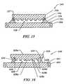
- FIG. 15shown is a simplified cross section of a template transfer holder 540 having a template 526 coupled to the template transfer substrate 544 with a perimeter of solid imprint material 534 according to another embodiment of the present invention to fixedly attach template transfer substrate 544 to template 526 .
- the entire mold pattern 528may be encapsulated, e.g., hermetically sealed as discussed above with respect to FIG. 14 .
- template 526may, optionally, include a perimeter mesa 536 that forms a perimeter recess 537 around the mold pattern 528 .
- Imprint material 534does not adhere to a mold pattern 528 on template 526 , thus facilitating mold fidelity.
- a selected volume of imprinting material 534is applied in a fluid state to a surface 531 of template transfer substrate 544 .
- the imprinting material 534may be applied to a selected area (e.g. an area corresponding to the perimeter of template 526 ), or the volume of imprinting material 534 is selected to adhere to the perimeter mesa 536 only, and to not fill in areas of mold pattern 528 on template 526 .
- Recess 537prevents fluid imprinting material 534 from reaching mold pattern 528 when mechanical contact is made between the imprinting material 534 and template 526 .
- FIG. 16is a simplified cross section of a template transfer assembly 640 having a template 626 , a mesa 636 and a major surface 626 a disposed opposite to the mesa 636 .
- a mold pattern 628is included on the mesa 636 as having grooves 628 a and protrusions 628 b .
- the grooves 628 ainclude a nadir surface 628 c and the protrusions 628 b include an apex surface 628 d .
- a surface 638circumscribes, if not all, then a subset of the grooves 628 a and the protrusions 628 b .
- nadir surfaces 628 care spaced apart from major surface 626 a a first distance d 1
- one or more apex surfaces 628 dare spaced-apart from major surface 626 a a second distance, d 2
- Surface 638is spaced apart from major surface 626 a a third distance, d 3
- Mesa 636is defined by ensuring third distance d 3 differs from both first and second distances, d 1 and d 2 . In the specific example, distance d 3 is less than either of distances d 1 and d 2 .
- Imprinting material 634is disposed in regions between surface 638 and surface 631 of template transfer substrate 644 .
- imprint material 634may be employed to maintain a fixed position between template 626 and template transfer substrate 644 without imprint material 634 contacting mold pattern 628 on template 626 . Additionally, imprinting material 634 may be disposed so as to encapsulate mold pattern 628 , e.g., hermetically seal the same, as discussed above. In this manner, mold pattern 628 is protected from physical damage and contamination.
- a selected volume of imprinting material 634is applied in a fluid state to a surface 631 of template transfer substrate 644 .
- the imprinting material 634is applied to a region of surface 631 that will be in superimposition with surface 638 .
- the volume of imprinting material 634 typically selectedis sufficient to adhere template 626 to the template transfer substrate 644 so that mold pattern 628 is spaced-apart from surface 631 .
- imprinting material 634may circumscribe mold pattern 628 , thereby encapsulating the same to prevent contamination by particulate matter.
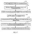
- template 26is loaded onto template transfer system 40 at step 702 .
- Template 26is moved to a position beneath an imprint head 18 at step 704 and the spacing between the imprint head 18 and template 26 is reduced at step 706 to place the imprint head 18 in close proximity, or in contact, with the template 26 .
- the template 26is secured to the imprint head 18 at step 708 , and the distance between template transfer holder 40 a and imprint head 18 is increased at step 710 .
- the template transfer holder 40 ais moved to a second position that is not beneath the imprint head 18 at step 712 .
- the template transfer holder 40 ais removed from the motion stage 20 at step 714 and a process wafer 30 is loaded on a wafer chuck 21 of the motion stage 20 for imprinting with the template 26 .
- a process wafer 30is loaded on a wafer chuck 21 of the motion stage 20 for imprinting with the template 26 .
- FIG. 18is a simplified flow chart of a method 720 of removing a template 26 , shown in FIG. 1, from an imprint head 18 in an imprint lithography system 10 , according to another embodiment of the present invention.
- a template transfer substratesuch as template transfer substrates 144 , 244 , 344 , 444 , 544 and 644 , shown in FIGS. 11, 12 , 13 , 14 , 15 and 16 , respectively, may be employed.
- the present exampleis discussed with respect to template transfer substrate 444 , shown in FIG. 14, and applies with equal weight to the aforementioned template transfer substrates.
- template transfer substrate 444is loaded onto a wafer chuck 21 in imprint lithography system 10 .
- a selected volume of imprinting fluidis dispensed onto the surface of the template transfer substrate 444 at step 724 .
- Relative movement between the imprint head 18 holding a template 26 and the template transfer substrate 444is achieved so that the template 26 contacts the imprinting fluid at step 726 .
- the imprinting fluidis converted to solid imprint material at step 728 .
- the template 26is released from the imprint head 18 (e.g. by turning off the securing means and raising the imprint head 18 ) and the template transfer substrate 444 with the attached template 26 is removed from the wafer chuck 21 and transferred to a storage location at step 730 .
- the template 26remains attached to the template transfer substrate 444 on the wafer chuck 21 and the imprint head 18 and the template 26 are arranged to be spaced-apart at step 730 a .
- the template 26is left in the imprint head 18 attached to the template transfer substrate 444 for storage on the wafer chuck 21 at step 730 b.
- FIG. 19is a simplified flow chart of a method 740 of installing a template 26 , shown in FIG. 1, from a template transfer substrate 444 , shown in FIG. 14, into an imprint head 18 of an imprint lithography system 10 , according to yet another embodiment of the present invention.
- a template transfer substrate 444 with a template 26 adhered to the template transfer substrate 444 with imprint material 434is provided at step 742 .
- the template transfer substrate 444is loaded onto a wafer chuck 21 of a wafer 30 in imprint lithography system 10 at step 744 .
- the template transfer substrate 444is already on the wafer chuck 21 , as when the template 26 is stored in this fashion between uses.
- the wafer chuck 21is moved to position the template 26 beneath an imprint head 18 of the wafer 30 in imprint lithography system 10 at step 746 .
- a template 26 stored on a template transfer substrate 444is already beneath the imprint head 18 . Relative movement between the imprint head 18 and the template 26 is achieved to place the imprint head 18 and template 26 in close proximity or contact at step 748 .
- the template 26is secured to the imprint head 18 at step 750 .
- the distance between imprint head 18 and template transfer substrate 444is increased at step 752 , releasing the template 26 from the imprint material 434 .
- the template transfer substrate 444is removed from the wafer chuck 21 and a process wafer 30 may then be loaded onto the wafer chuck 21 for imprinting with the template 26 .
Landscapes
- Engineering & Computer Science (AREA)
- Chemical & Material Sciences (AREA)
- Nanotechnology (AREA)
- Physics & Mathematics (AREA)
- General Physics & Mathematics (AREA)
- Crystallography & Structural Chemistry (AREA)
- Mathematical Physics (AREA)
- Theoretical Computer Science (AREA)
- Condensed Matter Physics & Semiconductors (AREA)
- Manufacturing & Machinery (AREA)
- Shaping Of Tube Ends By Bending Or Straightening (AREA)
- Exposure Of Semiconductors, Excluding Electron Or Ion Beam Exposure (AREA)
Abstract
Description
Claims (20)
Priority Applications (9)
| Application Number | Priority Date | Filing Date | Title |
|---|---|---|---|
| US10/438,224US6805054B1 (en) | 2003-05-14 | 2003-05-14 | Method, system and holder for transferring templates during imprint lithography processes |
| EP10151773AEP2177951A1 (en) | 2003-05-14 | 2004-05-11 | Method, system, holder and assembly for transferring templates during imprint lithography processes |
| KR1020057021605AKR101055640B1 (en) | 2003-05-14 | 2004-05-11 | Mold transfer methods, systems, holders and assemblies during an imprint lithography process |
| CNB2004800170543ACN100455449C (en) | 2003-05-14 | 2004-05-11 | Method, system, holder and assembly for transferring stencils in an imprint lithography process |
| JP2006532954AJP4937750B2 (en) | 2003-05-14 | 2004-05-11 | Method, system, holder, assembly for moving a template during an imprint lithography process |
| AT04751888TATE487579T1 (en) | 2003-05-14 | 2004-05-11 | METHOD, SYSTEM, HOLDER AND ARRANGEMENT FOR TRANSFERRING TEMPLATES IN IMPRINT LITHOGRAPHY PROCESSES |
| EP04751888AEP1622750B1 (en) | 2003-05-14 | 2004-05-11 | Method, system, holder and assembly for transferring templates during imprint lithography processes |
| PCT/US2004/014720WO2004103666A2 (en) | 2003-05-14 | 2004-05-11 | Method, system, holder and assembly for transferring templates during imprint lithography processes |
| DE602004030001TDE602004030001D1 (en) | 2003-05-14 | 2004-05-11 | METHOD, SYSTEM, HOLDER AND ARRANGEMENT FOR TRANSMITTING TEMPLATES IN IMPRINT LITHOGRAPHIC PROCEDURE |
Applications Claiming Priority (1)
| Application Number | Priority Date | Filing Date | Title |
|---|---|---|---|
| US10/438,224US6805054B1 (en) | 2003-05-14 | 2003-05-14 | Method, system and holder for transferring templates during imprint lithography processes |
Publications (1)
| Publication Number | Publication Date |
|---|---|
| US6805054B1true US6805054B1 (en) | 2004-10-19 |
Family
ID=33131515
Family Applications (1)
| Application Number | Title | Priority Date | Filing Date |
|---|---|---|---|
| US10/438,224Expired - LifetimeUS6805054B1 (en) | 2003-05-14 | 2003-05-14 | Method, system and holder for transferring templates during imprint lithography processes |
Country Status (2)
| Country | Link |
|---|---|
| US (1) | US6805054B1 (en) |
| CN (1) | CN100455449C (en) |
Cited By (37)
| Publication number | Priority date | Publication date | Assignee | Title |
|---|---|---|---|---|
| US20050214398A1 (en)* | 2003-05-14 | 2005-09-29 | Molecular Imprints, Inc | Assembly and method for transferring imprint lithography templates |
| US20050212156A1 (en)* | 2004-03-29 | 2005-09-29 | Toshinobu Tokita | Processing apparatus |
| US20050275125A1 (en)* | 2004-06-11 | 2005-12-15 | Eigo Kawakami | Processing apparatus and method |
| US20060032070A1 (en)* | 2004-08-11 | 2006-02-16 | Biggs Todd L | Micro tool alignment apparatus and method |
| US20060137555A1 (en)* | 2004-12-23 | 2006-06-29 | Asml Netherlands B.V. | Imprint lithography |
| US20060150849A1 (en)* | 2004-12-30 | 2006-07-13 | Asml Netherlands B.V. | Imprint lithography |
| US20060172031A1 (en)* | 2005-01-31 | 2006-08-03 | Molecular Imprints, Inc. | Chucking system for nano-manufacturing |
| US20060196377A1 (en)* | 2005-03-07 | 2006-09-07 | Asml Netherlands B.V. | Imprint lithography |
| US7122079B2 (en) | 2004-02-27 | 2006-10-17 | Molecular Imprints, Inc. | Composition for an etching mask comprising a silicon-containing material |
| US7136150B2 (en) | 2003-09-25 | 2006-11-14 | Molecular Imprints, Inc. | Imprint lithography template having opaque alignment marks |
| US20060255505A1 (en)* | 2005-05-11 | 2006-11-16 | Micron Technology, Inc. | Imprint templates for imprint lithography, and methods of patterning a plurality of substrates |
| US20070064384A1 (en)* | 2005-08-25 | 2007-03-22 | Molecular Imprints, Inc. | Method to transfer a template transfer body between a motion stage and a docking plate |
| US20070074635A1 (en)* | 2005-08-25 | 2007-04-05 | Molecular Imprints, Inc. | System to couple a body and a docking plate |
| US20070284779A1 (en)* | 2006-06-13 | 2007-12-13 | Wei Wu | Imprint lithography apparatus and methods |
| US20080122144A1 (en)* | 2006-11-28 | 2008-05-29 | Wei Zhang | Imprint lithography with improved substrate/mold separation |
| US20080145773A1 (en)* | 2006-10-10 | 2008-06-19 | Shih-Yuan Wang | Imprint lithography apparatus and methods |
| US7517211B2 (en) | 2005-12-21 | 2009-04-14 | Asml Netherlands B.V. | Imprint lithography |
| US20090146347A1 (en)* | 2007-12-06 | 2009-06-11 | Asml Netherlands B.V. | Imprint lithography |
| US7636999B2 (en)* | 2005-01-31 | 2009-12-29 | Molecular Imprints, Inc. | Method of retaining a substrate to a wafer chuck |
| US7665981B2 (en)* | 2005-08-25 | 2010-02-23 | Molecular Imprints, Inc. | System to transfer a template transfer body between a motion stage and a docking plate |
| US7670530B2 (en) | 2006-01-20 | 2010-03-02 | Molecular Imprints, Inc. | Patterning substrates employing multiple chucks |
| US7670529B2 (en) | 2005-12-08 | 2010-03-02 | Molecular Imprints, Inc. | Method and system for double-sided patterning of substrates |
| US20100237042A1 (en)* | 2009-03-23 | 2010-09-23 | Intevac, Inc. | Process for optimization of island to trench ratio in patterned media |
| US7803308B2 (en) | 2005-12-01 | 2010-09-28 | Molecular Imprints, Inc. | Technique for separating a mold from solidified imprinting material |
| US20110000882A1 (en)* | 2009-07-01 | 2011-01-06 | Nordson Corporation | Apparatus and methods for supporting workpieces during plasma processing |
| US20110018158A1 (en)* | 2009-07-22 | 2011-01-27 | Etienne Menard | Vacuum Coupled Tool Apparatus for Dry Transfer Printing Semiconductor Elements |
| US7906180B2 (en) | 2004-02-27 | 2011-03-15 | Molecular Imprints, Inc. | Composition for an etching mask comprising a silicon-containing material |
| US20120073461A1 (en)* | 2009-06-19 | 2012-03-29 | Shoichi Terada | Imprint system, imprint method, and non-transitory computer storage medium |
| US20120097336A1 (en)* | 2009-06-24 | 2012-04-26 | Tokyo Electron Limited | Template treatment apparatus and imprint system |
| US8349241B2 (en) | 2002-10-04 | 2013-01-08 | Molecular Imprints, Inc. | Method to arrange features on a substrate to replicate features having minimal dimensional variability |
| US20130112097A1 (en)* | 2011-10-14 | 2013-05-09 | Canon Kabushiki Kaisha | Imprint method imprint apparatus, and article manufacturing method |
| US8850980B2 (en) | 2006-04-03 | 2014-10-07 | Canon Nanotechnologies, Inc. | Tessellated patterns in imprint lithography |
| US9533445B2 (en) | 2010-01-22 | 2017-01-03 | Nanonex Corporation | Fast nanoimprinting methods using deformable mold |
| WO2018022190A1 (en)* | 2016-07-29 | 2018-02-01 | Molecular Imprints, Inc. | Substrate loading in microlithography |
| US10108086B2 (en) | 2013-03-15 | 2018-10-23 | Nanonex Corporation | System and methods of mold/substrate separation for imprint lithography |
| US10105883B2 (en) | 2013-03-15 | 2018-10-23 | Nanonex Corporation | Imprint lithography system and method for manufacturing |
| US11964421B1 (en)* | 2022-12-20 | 2024-04-23 | Canon Kabushiki Kaisha | Method and system for loading a superstrate onto a superstrate chuck |
Families Citing this family (1)
| Publication number | Priority date | Publication date | Assignee | Title |
|---|---|---|---|---|
| CN113073524B (en)* | 2021-04-22 | 2023-02-07 | 程力重工股份有限公司 | Imitative stone impression car of concrete of interchangeable template |
Citations (23)
| Publication number | Priority date | Publication date | Assignee | Title |
|---|---|---|---|---|
| US4610442A (en) | 1982-10-19 | 1986-09-09 | Matsushita Electric Industrial Co, Ltd. | Positioning table |
| US4724222A (en) | 1986-04-28 | 1988-02-09 | American Telephone And Telegraph Company, At&T Bell Laboratories | Wafer chuck comprising a curved reference surface |
| US4731155A (en) | 1987-04-15 | 1988-03-15 | General Electric Company | Process for forming a lithographic mask |
| US4763886A (en) | 1986-12-26 | 1988-08-16 | Nippon Thompson Co., Ltd. | XY-positioning table |
| US5669303A (en) | 1996-03-04 | 1997-09-23 | Motorola | Apparatus and method for stamping a surface |
| US5760500A (en) | 1996-03-28 | 1998-06-02 | Nippon Thompson Co., Ltd. | XY table using a linear electromagnetic actuator |
| US5772905A (en) | 1995-11-15 | 1998-06-30 | Regents Of The University Of Minnesota | Nanoimprint lithography |
| US5948470A (en) | 1997-04-28 | 1999-09-07 | Harrison; Christopher | Method of nanoscale patterning and products made thereby |
| US6039897A (en) | 1996-08-28 | 2000-03-21 | University Of Washington | Multiple patterned structures on a single substrate fabricated by elastomeric micro-molding techniques |
| US6180239B1 (en)* | 1993-10-04 | 2001-01-30 | President And Fellows Of Harvard College | Microcontact printing on surfaces and derivative articles |
| WO2001033232A2 (en) | 1999-11-05 | 2001-05-10 | Ion Diagnostics, Inc. | Precision stage |
| WO2001069317A1 (en) | 2000-03-15 | 2001-09-20 | Obducat Ab | Device for transferring a pattern to an object |
| WO2001079592A1 (en) | 2000-04-13 | 2001-10-25 | Obducat Aktiebolag | Apparatus and method for electrochemical processing of substrates |
| WO2001090816A1 (en) | 2000-05-24 | 2001-11-29 | Obducat Aktiebolag | Method in connection with the production of a template and the template thus produced |
| US6334960B1 (en) | 1999-03-11 | 2002-01-01 | Board Of Regents, The University Of Texas System | Step and flash imprint lithography |
| US20020115002A1 (en)* | 2000-10-12 | 2002-08-22 | Todd Bailey | Template for room temperature, low pressure micro-and nano-imprint lithography |
| US20020142229A1 (en)* | 2001-03-28 | 2002-10-03 | Motorola Inc. | Lithographic template and method of formation and use |
| US20020150398A1 (en)* | 2000-08-21 | 2002-10-17 | Choi Byung J. | Flexure based macro motion translation stage |
| US6518189B1 (en)* | 1995-11-15 | 2003-02-11 | Regents Of The University Of Minnesota | Method and apparatus for high density nanostructures |
| US20030219992A1 (en)* | 2002-05-22 | 2003-11-27 | Schaper Charles Daniel | Replication and transfer of microstructures and nanostructures |
| US20040022888A1 (en)* | 2002-08-01 | 2004-02-05 | Sreenivasan Sidlgata V. | Alignment systems for imprint lithography |
| US20040053146A1 (en)* | 2000-07-16 | 2004-03-18 | University Of Texas System Board Of Regents, Ut System | Method of varying template dimensions to achieve alignment during imprint lithography |
| US6716754B2 (en)* | 2002-03-12 | 2004-04-06 | Micron Technology, Inc. | Methods of forming patterns and molds for semiconductor constructions |
Family Cites Families (3)
| Publication number | Priority date | Publication date | Assignee | Title |
|---|---|---|---|---|
| CN2106713U (en)* | 1991-03-20 | 1992-06-10 | 张永铭 | Coloured stamping press |
| GB9817793D0 (en)* | 1998-08-14 | 1998-10-14 | Scherer Corp R P | The formation of indicia in the base of a blister pack for transference to a body cast therein |
| CN1262883C (en)* | 2000-07-17 | 2006-07-05 | 得克萨斯州大学系统董事会 | Method and system of automatic fluid dispensing for imprint lithography processes |
- 2003
- 2003-05-14USUS10/438,224patent/US6805054B1/ennot_activeExpired - Lifetime
- 2004
- 2004-05-11CNCNB2004800170543Apatent/CN100455449C/ennot_activeExpired - Lifetime
Patent Citations (24)
| Publication number | Priority date | Publication date | Assignee | Title |
|---|---|---|---|---|
| US4610442A (en) | 1982-10-19 | 1986-09-09 | Matsushita Electric Industrial Co, Ltd. | Positioning table |
| US4724222A (en) | 1986-04-28 | 1988-02-09 | American Telephone And Telegraph Company, At&T Bell Laboratories | Wafer chuck comprising a curved reference surface |
| US4763886A (en) | 1986-12-26 | 1988-08-16 | Nippon Thompson Co., Ltd. | XY-positioning table |
| US4731155A (en) | 1987-04-15 | 1988-03-15 | General Electric Company | Process for forming a lithographic mask |
| US6180239B1 (en)* | 1993-10-04 | 2001-01-30 | President And Fellows Of Harvard College | Microcontact printing on surfaces and derivative articles |
| US6518189B1 (en)* | 1995-11-15 | 2003-02-11 | Regents Of The University Of Minnesota | Method and apparatus for high density nanostructures |
| US5772905A (en) | 1995-11-15 | 1998-06-30 | Regents Of The University Of Minnesota | Nanoimprint lithography |
| US5669303A (en) | 1996-03-04 | 1997-09-23 | Motorola | Apparatus and method for stamping a surface |
| US5760500A (en) | 1996-03-28 | 1998-06-02 | Nippon Thompson Co., Ltd. | XY table using a linear electromagnetic actuator |
| US6039897A (en) | 1996-08-28 | 2000-03-21 | University Of Washington | Multiple patterned structures on a single substrate fabricated by elastomeric micro-molding techniques |
| US5948470A (en) | 1997-04-28 | 1999-09-07 | Harrison; Christopher | Method of nanoscale patterning and products made thereby |
| US6334960B1 (en) | 1999-03-11 | 2002-01-01 | Board Of Regents, The University Of Texas System | Step and flash imprint lithography |
| WO2001033232A2 (en) | 1999-11-05 | 2001-05-10 | Ion Diagnostics, Inc. | Precision stage |
| WO2001069317A1 (en) | 2000-03-15 | 2001-09-20 | Obducat Ab | Device for transferring a pattern to an object |
| WO2001079592A1 (en) | 2000-04-13 | 2001-10-25 | Obducat Aktiebolag | Apparatus and method for electrochemical processing of substrates |
| WO2001090816A1 (en) | 2000-05-24 | 2001-11-29 | Obducat Aktiebolag | Method in connection with the production of a template and the template thus produced |
| US20040053146A1 (en)* | 2000-07-16 | 2004-03-18 | University Of Texas System Board Of Regents, Ut System | Method of varying template dimensions to achieve alignment during imprint lithography |
| US20020150398A1 (en)* | 2000-08-21 | 2002-10-17 | Choi Byung J. | Flexure based macro motion translation stage |
| US20020115002A1 (en)* | 2000-10-12 | 2002-08-22 | Todd Bailey | Template for room temperature, low pressure micro-and nano-imprint lithography |
| US6696220B2 (en)* | 2000-10-12 | 2004-02-24 | Board Of Regents, The University Of Texas System | Template for room temperature, low pressure micro-and nano-imprint lithography |
| US20020142229A1 (en)* | 2001-03-28 | 2002-10-03 | Motorola Inc. | Lithographic template and method of formation and use |
| US6716754B2 (en)* | 2002-03-12 | 2004-04-06 | Micron Technology, Inc. | Methods of forming patterns and molds for semiconductor constructions |
| US20030219992A1 (en)* | 2002-05-22 | 2003-11-27 | Schaper Charles Daniel | Replication and transfer of microstructures and nanostructures |
| US20040022888A1 (en)* | 2002-08-01 | 2004-02-05 | Sreenivasan Sidlgata V. | Alignment systems for imprint lithography |
Non-Patent Citations (38)
| Title |
|---|
| Braeuer et al., "Precise Polymer Micro-Optical Systems," MRS Bulletin, Jul. 2001, pp. 519-522. |
| Choi et al., "Design of Orientation Stages for Step and Flash Imprint Lithography," Precision Engineering, Journal of the International Societies for Precision Engineering and Nanotechnology, 2001, pp. 192-199, vol. 25. |
| Choi et al., "Flexture Based Macro Motion Translation Stage," U.S. patent application 09/934,248, Filed with USPTO on Aug. 21, 2001. |
| Choi et al., "High Precision Orientation Alignment and Gap Control Stages for Imprint Lithography Processes," U.S. patent application 09/698,317, Filed with USPTO on Oct. 27, 2000. |
| Choi et al., "Method and System of Automatic Fluid Dispensing for Imprint Lithography Processes," U.S. patent application 09/908,455, Filed with USPTO on Jul. 17, 2001. |
| Choi et al., "Methods for High-Precision Gap and Orientation Sensing Between a Transparent Template and Substrate for Imprint Lithography," U.S. patent application 09/920,341, Filed with USPTO on Aug. 1, 2001. |
| Chou et al., "Imprint Lithography with 25-Nanometer Resolution," Science, Apr. 5, 1996, pp. 85-87, vol. 272. |
| Chou et al., "Imprint Lithography with Sub-10nm Feature Size and High Throughput," Microelectronic Engineering, 1997, pp. 237-240, vol. 35. |
| Chou et al., "Imprint of Sub-25 nm Vias and Trenches in Polymers," Applied Physics Letters, Nov. 20, 1995, pp. 3114-3116, vol. 67(21). |
| Chou et al., "Lithographically-Induced Self Assembly of Periodic Polymer Micropillar Arrays," Journal of Vacuum Science and Technology, Nov./Dec. 1999, pp. 3197-3202, vol. B 17(6). |
| Chou, "Nanoimprint Lithography and Lithographically Induced Self-Assembly," MRS Bulletin, Jul. 2001, pp. 512-517. |
| Colburn, et al., "Step and Flash Imprint Lithography: A New Approach to High-Resolution Patterning", Proc. of SPIE, 1999, pp. 379-389, vol. 3676. |
| Feldman et al., "Wafer chuck for manification correction in x-ray lithography," American Vacuum Society, 1998, pp. 3476-3479. |
| Haisma et al., "Mold-Assisted Nanolithography: A Process for Reliable Pattern Replication," Journal of Vacuum Science and Technology, Nov./Dec. 1996, pp. 4124-4126, vol. B 14(6). |
| Hogan, "Impedance Control: An Approach to Manipulation," Journal of Dynamic Systems, Measurement and Control, Mar. 1985, pp. 1-17, vol. 107. |
| Hollis et al., "A Six-Degree-of-Freedom Magnetically Levitated Variable Compliance Fine Motion Wrist: Design, Modeling and Control," IEEE Transactions on Robotics and Automation, 1991, pp. 320-332, vol. 7, No. 3. |
| Howell et al., "Loop-Closure Theory for the Analysis and Synthesis of Compilant Mechanisms," Journal of Mechanical Design, Mar. 1996, pp. 121-125, vol. 118. |
| Kanetomo et al., "Robot for Use in Ultrahigh Vacuum," Solid State Tech., Aug. 1997, pp. 63-64, 69-72. |
| Kim et al., "High Precision Magnetic Levitation Stage for Photolithography," Precision Engineering, 1998, pp. 66-77, vol. 22, Elsevier Science Inc., 655 Avenue of the Americas, NY, NY 10010. |
| Koseki et al., "Design and Accuracy Evaluation of High-Speed and High-Precision Parallel Mechanism," Proc. of the 1998 IEEE, Intl. Conf. on Robotics & Automation, May 1998, pp. 1340-1345, Leuven, Belgium. |
| Krauss et al., "Fabrication of Nanodevices Using Sub-25nm Imprint Lithography," Appl. Phys. Lett 67(21), 3114-3116, 1995. |
| Lee et al., "An Ultraprecision Stage for Alignment of Wafers in Advanced Microlithography," Precision Engineering, 1997, pp. 113-122, vol. 21, Elsevier Science Inc., 655 Avenue of the Americas, NY, NY 10010. |
| Lee et al., "Ultra Precision Positioning System for Servo Motor-Piezo Actuator Using the Dual Servo Loop and Digital Filter Implementation," ASPE, 1998, pp. 287-290, vol. 18. |
| Meissl et al., "An Assembly And Method For Transfering Imprint Lithography Templates," U.S. patent application 10/437,476, Filed with USPTO May 14, 2003. |
| Merlet, "Parallel Manipulators: State of the Art Perspectives," Advanced Robotics, 1994, pp. 589-596, vol. 8. |
| Mirkin et al., "Emerging Methods for Micro-and Nanofabrication," MRS Bulletin, Jul. 2001, pp. 506-509. |
| Mittal et al., "Precision Motion Control of Magnetic Suspension Acutator Using a Robust Nonlinear Compensation Scheme," IEEE/ASME Transactions on Mechatronics, Dec. 1997, pp. 268-280, vol. 2, No. 4. |
| Ohya et al., "Development of 3-DOF Finger Module for Micro Manipulation," Proc. of the 1999 IEEE/RSJ, Intl. Conf. on Intelligent Robots and Systems, 1999, pp. 894-899. |
| Raibert et al., "Hybrid Position/Force Control of Manipulators," Transactions of the ASME, Journal of Dynamic Systems, Measurement and Control, June 1981, pp. 126-133, vol. 102. |
| Rong et al., "Dynamics of Parallel Mechanism with Direct Compliance Control," IEEE, 1997, pp. 1753-1758. |
| Ruchhoeft et al., "Patterning Curved Surfaces: Template Generation by Ion Beam Proximity Lithography and Relief Transfer by Step and Flash Imprint Lithography," Journal of Vacuum Science and Technology, 1999, pp. 2965-2982, vol. 17. |
| Slocum, "Precision Machine Design: Macromachine Design Philosophy and its Applicability to the Design of Micromachines," Micro Electro Mechanical Systems, 1992, pp. 37-42. |
| Sreenivasan et al., "High-Resolution Overlay Alignment Methods and Systems for Imprint Lithography," U.S. patent application 09/907,512, Filed with USPTO on Jul. 16, 2001. |
| Sreenivasan et al., "Step and Repeat Imprint Lithography Processes," U.S. patent application 10/194,991, Filed with USPTO Jul. 11, 2002. |
| Sreenivasan et al., "Step and Repeat Imprint Lithography Systems," U.S. patent application 10/194,414, Filed with USPTO Jul. 11, 2002. |
| Tajbakhsh et al., "Three-Degree-of-Freedom Optic Mount for Extreme Ultraviolet Lithography," ASPE, 1998, pp. 359-362, vol. 18. |
| Tanikawa et al., "Development of Small-Sized 3 DOF Finger Moldule in Micro Hand for Micro Manipulation," Proc. of the IEEE/RSJ, Intl. Conf. on Intelligent Robots and Systems, 1999, pp. 876-881. |
| Tomita et al., "A 6-Axes Motion Control Method for Parallel-Linkage-Type Fine Motion Stage," Journal of Japan Society of Precision Engineering, 1992. pp. 118-124. |
Cited By (73)
| Publication number | Priority date | Publication date | Assignee | Title |
|---|---|---|---|---|
| US8349241B2 (en) | 2002-10-04 | 2013-01-08 | Molecular Imprints, Inc. | Method to arrange features on a substrate to replicate features having minimal dimensional variability |
| US6951173B1 (en)* | 2003-05-14 | 2005-10-04 | Molecular Imprints, Inc. | Assembly and method for transferring imprint lithography templates |
| US20050214398A1 (en)* | 2003-05-14 | 2005-09-29 | Molecular Imprints, Inc | Assembly and method for transferring imprint lithography templates |
| US7136150B2 (en) | 2003-09-25 | 2006-11-14 | Molecular Imprints, Inc. | Imprint lithography template having opaque alignment marks |
| US7906180B2 (en) | 2004-02-27 | 2011-03-15 | Molecular Imprints, Inc. | Composition for an etching mask comprising a silicon-containing material |
| US7122079B2 (en) | 2004-02-27 | 2006-10-17 | Molecular Imprints, Inc. | Composition for an etching mask comprising a silicon-containing material |
| US20050212156A1 (en)* | 2004-03-29 | 2005-09-29 | Toshinobu Tokita | Processing apparatus |
| US7815425B2 (en) | 2004-03-29 | 2010-10-19 | Canon Kabushiki Kaisha | Processing apparatus |
| US20050275125A1 (en)* | 2004-06-11 | 2005-12-15 | Eigo Kawakami | Processing apparatus and method |
| US7789647B2 (en)* | 2004-06-11 | 2010-09-07 | Canon Kabushiki Kaisha | Processing apparatus and method |
| US7162810B2 (en)* | 2004-08-11 | 2007-01-16 | Intel Corporation | Micro tool alignment apparatus and method |
| US20060032070A1 (en)* | 2004-08-11 | 2006-02-16 | Biggs Todd L | Micro tool alignment apparatus and method |
| US20100050893A1 (en)* | 2004-12-23 | 2010-03-04 | Asml Netherlands B.V. | Imprint lithography |
| US7676088B2 (en)* | 2004-12-23 | 2010-03-09 | Asml Netherlands B.V. | Imprint lithography |
| US8131078B2 (en) | 2004-12-23 | 2012-03-06 | Asml Netherlands B.V. | Imprint lithography |
| US20060137555A1 (en)* | 2004-12-23 | 2006-06-29 | Asml Netherlands B.V. | Imprint lithography |
| US8571318B2 (en) | 2004-12-23 | 2013-10-29 | Asml Netherlands B.V. | Imprint lithography |
| US7636475B2 (en) | 2004-12-23 | 2009-12-22 | Asml Netherlands B.V. | Imprint lithography |
| US20060150849A1 (en)* | 2004-12-30 | 2006-07-13 | Asml Netherlands B.V. | Imprint lithography |
| US7490547B2 (en)* | 2004-12-30 | 2009-02-17 | Asml Netherlands B.V. | Imprint lithography |
| US20060172031A1 (en)* | 2005-01-31 | 2006-08-03 | Molecular Imprints, Inc. | Chucking system for nano-manufacturing |
| US7636999B2 (en)* | 2005-01-31 | 2009-12-29 | Molecular Imprints, Inc. | Method of retaining a substrate to a wafer chuck |
| US7798801B2 (en) | 2005-01-31 | 2010-09-21 | Molecular Imprints, Inc. | Chucking system for nano-manufacturing |
| US7523701B2 (en)* | 2005-03-07 | 2009-04-28 | Asml Netherlands B.V. | Imprint lithography method and apparatus |
| US20090174115A1 (en)* | 2005-03-07 | 2009-07-09 | Asml Netherlands B.V. | Imprint lithography |
| US20060196377A1 (en)* | 2005-03-07 | 2006-09-07 | Asml Netherlands B.V. | Imprint lithography |
| US7906059B2 (en)* | 2005-03-07 | 2011-03-15 | Asml Netherlands B.V. | Imprint lithography |
| US20060255505A1 (en)* | 2005-05-11 | 2006-11-16 | Micron Technology, Inc. | Imprint templates for imprint lithography, and methods of patterning a plurality of substrates |
| US7767129B2 (en) | 2005-05-11 | 2010-08-03 | Micron Technology, Inc. | Imprint templates for imprint lithography, and methods of patterning a plurality of substrates |
| US7665981B2 (en)* | 2005-08-25 | 2010-02-23 | Molecular Imprints, Inc. | System to transfer a template transfer body between a motion stage and a docking plate |
| US20070064384A1 (en)* | 2005-08-25 | 2007-03-22 | Molecular Imprints, Inc. | Method to transfer a template transfer body between a motion stage and a docking plate |
| US20070074635A1 (en)* | 2005-08-25 | 2007-04-05 | Molecular Imprints, Inc. | System to couple a body and a docking plate |
| US7803308B2 (en) | 2005-12-01 | 2010-09-28 | Molecular Imprints, Inc. | Technique for separating a mold from solidified imprinting material |
| US7670529B2 (en) | 2005-12-08 | 2010-03-02 | Molecular Imprints, Inc. | Method and system for double-sided patterning of substrates |
| US20090212462A1 (en)* | 2005-12-21 | 2009-08-27 | Asml Netherlans B.V. | Imprint lithography |
| US8753557B2 (en) | 2005-12-21 | 2014-06-17 | Asml Netherlands B.V. | Imprint lithography |
| US7517211B2 (en) | 2005-12-21 | 2009-04-14 | Asml Netherlands B.V. | Imprint lithography |
| US9610727B2 (en) | 2005-12-21 | 2017-04-04 | Asml Netherlands B.V. | Imprint lithography |
| US8100684B2 (en) | 2005-12-21 | 2012-01-24 | Asml Netherlands B.V. | Imprint lithography |
| US7670530B2 (en) | 2006-01-20 | 2010-03-02 | Molecular Imprints, Inc. | Patterning substrates employing multiple chucks |
| US8850980B2 (en) | 2006-04-03 | 2014-10-07 | Canon Nanotechnologies, Inc. | Tessellated patterns in imprint lithography |
| US20070284779A1 (en)* | 2006-06-13 | 2007-12-13 | Wei Wu | Imprint lithography apparatus and methods |
| US20080145773A1 (en)* | 2006-10-10 | 2008-06-19 | Shih-Yuan Wang | Imprint lithography apparatus and methods |
| US7832416B2 (en) | 2006-10-10 | 2010-11-16 | Hewlett-Packard Development Company, L.P. | Imprint lithography apparatus and methods |
| WO2008067394A3 (en)* | 2006-11-28 | 2008-08-14 | Nanonex Corp | Imprint lithography with improved substrate/mold separation |
| US8377361B2 (en) | 2006-11-28 | 2013-02-19 | Wei Zhang | Imprint lithography with improved substrate/mold separation |
| US20080122144A1 (en)* | 2006-11-28 | 2008-05-29 | Wei Zhang | Imprint lithography with improved substrate/mold separation |
| US20090146347A1 (en)* | 2007-12-06 | 2009-06-11 | Asml Netherlands B.V. | Imprint lithography |
| US8524136B2 (en)* | 2007-12-06 | 2013-09-03 | Asml Netherlands B.V. | Imprint lithography |
| US20100237042A1 (en)* | 2009-03-23 | 2010-09-23 | Intevac, Inc. | Process for optimization of island to trench ratio in patterned media |
| US8715515B2 (en) | 2009-03-23 | 2014-05-06 | Intevac, Inc. | Process for optimization of island to trench ratio in patterned media |
| TWI469864B (en)* | 2009-06-19 | 2015-01-21 | Tokyo Electron Ltd | Imprint system, imprint method, program and computer recording medium |
| US20120073461A1 (en)* | 2009-06-19 | 2012-03-29 | Shoichi Terada | Imprint system, imprint method, and non-transitory computer storage medium |
| US8888920B2 (en)* | 2009-06-19 | 2014-11-18 | Tokyo Electron Limited | Imprint system, imprint method, and non-transitory computer storage medium |
| US8840728B2 (en)* | 2009-06-24 | 2014-09-23 | Tokyo Electron Limited | Imprint system for performing a treatment on a template |
| US20120097336A1 (en)* | 2009-06-24 | 2012-04-26 | Tokyo Electron Limited | Template treatment apparatus and imprint system |
| US20110000882A1 (en)* | 2009-07-01 | 2011-01-06 | Nordson Corporation | Apparatus and methods for supporting workpieces during plasma processing |
| US10026436B2 (en) | 2009-07-01 | 2018-07-17 | Nordson Corporation | Apparatus and methods for supporting workpieces during plasma processing |
| US20110018158A1 (en)* | 2009-07-22 | 2011-01-27 | Etienne Menard | Vacuum Coupled Tool Apparatus for Dry Transfer Printing Semiconductor Elements |
| US8261660B2 (en)* | 2009-07-22 | 2012-09-11 | Semprius, Inc. | Vacuum coupled tool apparatus for dry transfer printing semiconductor elements |
| US9533445B2 (en) | 2010-01-22 | 2017-01-03 | Nanonex Corporation | Fast nanoimprinting methods using deformable mold |
| US20130112097A1 (en)* | 2011-10-14 | 2013-05-09 | Canon Kabushiki Kaisha | Imprint method imprint apparatus, and article manufacturing method |
| US9566741B2 (en) | 2011-10-14 | 2017-02-14 | Canon Kabushiki Kaisha | Imprint method, imprint apparatus, and article manufacturing method |
| US9892949B2 (en) | 2011-10-14 | 2018-02-13 | Canon Kabushiki Kaisha | Imprint method, imprint apparatus, and article manufacturing method |
| US9201298B2 (en)* | 2011-10-14 | 2015-12-01 | Canon Kabushiki Kaisha | Imprint method, imprint apparatus, and article manufacturing method |
| US10108086B2 (en) | 2013-03-15 | 2018-10-23 | Nanonex Corporation | System and methods of mold/substrate separation for imprint lithography |
| US10105883B2 (en) | 2013-03-15 | 2018-10-23 | Nanonex Corporation | Imprint lithography system and method for manufacturing |
| WO2018022190A1 (en)* | 2016-07-29 | 2018-02-01 | Molecular Imprints, Inc. | Substrate loading in microlithography |
| US10025202B2 (en) | 2016-07-29 | 2018-07-17 | Molecular Imprints, Inc. | Substrate loading in microlithography |
| CN109804309A (en)* | 2016-07-29 | 2019-05-24 | 分子印记公司 | Substrate loading in microlithography |
| US10317806B2 (en) | 2016-07-29 | 2019-06-11 | Molecular Imprints, Inc. | Substrate loading in microlithography |
| CN109804309B (en)* | 2016-07-29 | 2022-09-02 | 分子印记公司 | Substrate loading in microlithography |
| US11964421B1 (en)* | 2022-12-20 | 2024-04-23 | Canon Kabushiki Kaisha | Method and system for loading a superstrate onto a superstrate chuck |
Also Published As
| Publication number | Publication date |
|---|---|
| CN1809468A (en) | 2006-07-26 |
| CN100455449C (en) | 2009-01-28 |
Similar Documents
| Publication | Publication Date | Title |
|---|---|---|
| US6805054B1 (en) | Method, system and holder for transferring templates during imprint lithography processes | |
| US6951173B1 (en) | Assembly and method for transferring imprint lithography templates | |
| US7906058B2 (en) | Bifurcated contact printing technique | |
| US7803308B2 (en) | Technique for separating a mold from solidified imprinting material | |
| US8033815B2 (en) | Chucking system for nano-manufacturing | |
| US7298456B2 (en) | System for varying dimensions of a substrate during nanoscale manufacturing | |
| US10105883B2 (en) | Imprint lithography system and method for manufacturing | |
| US20090273119A1 (en) | Imprint Method and Imprint Apparatus | |
| US20040104641A1 (en) | Method of separating a template from a substrate during imprint lithography | |
| EP1622750B1 (en) | Method, system, holder and assembly for transferring templates during imprint lithography processes | |
| JP2750554B2 (en) | Vacuum suction device | |
| US8334967B2 (en) | Substrate support system having a plurality of contact lands | |
| KR102802323B1 (en) | Substrate transportation hand, substrate transportation system, storage medium, and method for producing article | |
| CN120344909A (en) | Apparatus and method for processing substrates in a vacuum processing space | |
| Lu et al. | High-efficient Chip to Wafer Self-alignment and Bonding for Flexible and Size-free MEMS-IC Integration |
Legal Events
| Date | Code | Title | Description |
|---|---|---|---|
| AS | Assignment | Owner name:MOLECULAR IMPRINTYS, INC., TEXAS Free format text:ASSIGNMENT OF ASSIGNORS INTEREST;ASSIGNORS:MEISSL, MARIO J.;CHOI, BYUNG JIN;BABBS, DANIEL;AND OTHERS;REEL/FRAME:014080/0339 Effective date:20030514 | |
| STCF | Information on status: patent grant | Free format text:PATENTED CASE | |
| AS | Assignment | Owner name:VENTURE LENDING & LEASING IV, INC., CALIFORNIA Free format text:SECURITY INTEREST;ASSIGNOR:MOLECULAR IMPRINTS, INC.;REEL/FRAME:016133/0369 Effective date:20040928 Owner name:VENTURE LENDING & LEASING IV, INC.,CALIFORNIA Free format text:SECURITY INTEREST;ASSIGNOR:MOLECULAR IMPRINTS, INC.;REEL/FRAME:016133/0369 Effective date:20040928 | |
| AS | Assignment | Owner name:MOLECULAR IMPRINTS INC., TEXAS Free format text:CORRECTION OF STATE OF INCORPORATION OF THE ASSIGNEE RECITED ON THE ASSIGNMENT FROM TEXAS TO DELAWARE, RECORDED AT REE/FRAME 014080/0339.;ASSIGNORS:MEISSL, MARIO J.;CHOI, BYUNG JIN;BABBS, DANIEL;AND OTHERS;REEL/FRAME:015621/0890;SIGNING DATES FROM 20030513 TO 20030514 | |
| CC | Certificate of correction | ||
| AS | Assignment | Owner name:MOLECULAR IMPRINTS, INC.,TEXAS Free format text:RELEASE BY SECURED PARTY;ASSIGNOR:VENTURE LENDING & LEASING IV, INC.;REEL/FRAME:019072/0882 Effective date:20070326 Owner name:MOLECULAR IMPRINTS, INC., TEXAS Free format text:RELEASE BY SECURED PARTY;ASSIGNOR:VENTURE LENDING & LEASING IV, INC.;REEL/FRAME:019072/0882 Effective date:20070326 | |
| FPAY | Fee payment | Year of fee payment:4 | |
| REMI | Maintenance fee reminder mailed | ||
| AS | Assignment | Owner name:CANON INC., JAPAN Free format text:ASSIGNMENT OF ASSIGNORS INTEREST;ASSIGNOR:MOLECULAR IMPRINTS, INC.;REEL/FRAME:026842/0929 Effective date:20110901 | |
| FPAY | Fee payment | Year of fee payment:8 | |
| AS | Assignment | Owner name:CANON INC., JAPAN Free format text:CORRECTIVE ASSIGNMENT TO CORRECT THE NATURE OF CONVEYANCE FROM AN "ASSIGNMENT" TO "SECURITY AGREEMENT" PREVIOUSLY RECORDED ON REEL 026842 FRAME 0929. ASSIGNOR(S) HEREBY CONFIRMS THE THE ORIGINAL DOCUMENT SUBMITTED WAS A "SECURITY AGREEMENT";ASSIGNOR:MOLECULAR IMPRINTS, INC.;REEL/FRAME:031003/0031 Effective date:20110901 | |
| AS | Assignment | Owner name:CANON INC., JAPAN Free format text:RELEASE OF SECURITY INTEREST;ASSIGNOR:MOLECULAR IMPRINTS, INC.;REEL/FRAME:033161/0705 Effective date:20140613 | |
| AS | Assignment | Owner name:MOLECULAR IMPRINTS, INC., TEXAS Free format text:CORRECTIVE ASSIGNMENT TO CORRECT THE ASSIGNOR AND ASSIGNEE PREVIOUSLY RECORDED ON REEL 033161 FRAME 0705. ASSIGNOR(S) HEREBY CONFIRMS THE ASSIGNMENT;ASSIGNOR:CANON INC.;REEL/FRAME:033227/0398 Effective date:20140613 | |
| AS | Assignment | Owner name:MII NEWCO, INC., TEXAS Free format text:ASSIGNMENT OF JOINT OWNERSHIP;ASSIGNOR:MOLECULAR IMPRINTS, INC.;REEL/FRAME:033329/0280 Effective date:20140710 | |
| AS | Assignment | Owner name:CANON NANOTECHNOLOGIES, INC., TEXAS Free format text:CHANGE OF NAME;ASSIGNOR:MOLECULAR IMPRINTS, INC.;REEL/FRAME:033400/0184 Effective date:20140417 | |
| AS | Assignment | Owner name:MOLECULAR IMPRINTS, INC., TEXAS Free format text:CHANGE OF NAME;ASSIGNOR:MII NEWCO, INC.;REEL/FRAME:033449/0684 Effective date:20140423 | |
| AS | Assignment | Owner name:MOLECULAR IMPRINTS, INC., TEXAS Free format text:CONFIRMATORY ASSIGNMENT OF JOINT PATENT OWNERSHIP;ASSIGNOR:CANON NANOTECHNOLOGIES, INC.;REEL/FRAME:035507/0559 Effective date:20150427 | |
| FPAY | Fee payment | Year of fee payment:12 | |
| AS | Assignment | Owner name:JP MORGAN CHASE BANK, N.A., NEW YORK Free format text:PATENT SECURITY AGREEMENT;ASSIGNORS:MAGIC LEAP, INC.;MOLECULAR IMPRINTS, INC.;MENTOR ACQUISITION ONE, LLC;REEL/FRAME:050138/0287 Effective date:20190820 | |
| AS | Assignment | Owner name:CITIBANK, N.A., NEW YORK Free format text:ASSIGNMENT OF SECURITY INTEREST IN PATENTS;ASSIGNOR:JPMORGAN CHASE BANK, N.A.;REEL/FRAME:050967/0138 Effective date:20191106 |