US6804125B2 - Isolated drive circuitry used in switch-mode power converters - Google Patents
Isolated drive circuitry used in switch-mode power convertersDownload PDFInfo
- Publication number
- US6804125B2 US6804125B2US10/061,189US6118902AUS6804125B2US 6804125 B2US6804125 B2US 6804125B2US 6118902 AUS6118902 AUS 6118902AUS 6804125 B2US6804125 B2US 6804125B2
- Authority
- US
- United States
- Prior art keywords
- primary
- switch
- input
- power
- drive transformer
- Prior art date
- Legal status (The legal status is an assumption and is not a legal conclusion. Google has not performed a legal analysis and makes no representation as to the accuracy of the status listed.)
- Expired - Lifetime, expires
Links
Images


Classifications
- H—ELECTRICITY
- H02—GENERATION; CONVERSION OR DISTRIBUTION OF ELECTRIC POWER
- H02M—APPARATUS FOR CONVERSION BETWEEN AC AND AC, BETWEEN AC AND DC, OR BETWEEN DC AND DC, AND FOR USE WITH MAINS OR SIMILAR POWER SUPPLY SYSTEMS; CONVERSION OF DC OR AC INPUT POWER INTO SURGE OUTPUT POWER; CONTROL OR REGULATION THEREOF
- H02M1/00—Details of apparatus for conversion
- H02M1/08—Circuits specially adapted for the generation of control voltages for semiconductor devices incorporated in static converters
- H02M1/088—Circuits specially adapted for the generation of control voltages for semiconductor devices incorporated in static converters for the simultaneous control of series or parallel connected semiconductor devices
- H—ELECTRICITY
- H02—GENERATION; CONVERSION OR DISTRIBUTION OF ELECTRIC POWER
- H02M—APPARATUS FOR CONVERSION BETWEEN AC AND AC, BETWEEN AC AND DC, OR BETWEEN DC AND DC, AND FOR USE WITH MAINS OR SIMILAR POWER SUPPLY SYSTEMS; CONVERSION OF DC OR AC INPUT POWER INTO SURGE OUTPUT POWER; CONTROL OR REGULATION THEREOF
- H02M1/00—Details of apparatus for conversion
- H02M1/38—Means for preventing simultaneous conduction of switches
- H—ELECTRICITY
- H02—GENERATION; CONVERSION OR DISTRIBUTION OF ELECTRIC POWER
- H02M—APPARATUS FOR CONVERSION BETWEEN AC AND AC, BETWEEN AC AND DC, OR BETWEEN DC AND DC, AND FOR USE WITH MAINS OR SIMILAR POWER SUPPLY SYSTEMS; CONVERSION OF DC OR AC INPUT POWER INTO SURGE OUTPUT POWER; CONTROL OR REGULATION THEREOF
- H02M3/00—Conversion of DC power input into DC power output
- H02M3/22—Conversion of DC power input into DC power output with intermediate conversion into AC
- H02M3/24—Conversion of DC power input into DC power output with intermediate conversion into AC by static converters
- H02M3/28—Conversion of DC power input into DC power output with intermediate conversion into AC by static converters using discharge tubes with control electrode or semiconductor devices with control electrode to produce the intermediate AC
- H02M3/325—Conversion of DC power input into DC power output with intermediate conversion into AC by static converters using discharge tubes with control electrode or semiconductor devices with control electrode to produce the intermediate AC using devices of a triode or a transistor type requiring continuous application of a control signal
- H02M3/335—Conversion of DC power input into DC power output with intermediate conversion into AC by static converters using discharge tubes with control electrode or semiconductor devices with control electrode to produce the intermediate AC using devices of a triode or a transistor type requiring continuous application of a control signal using semiconductor devices only
- H02M3/33569—Conversion of DC power input into DC power output with intermediate conversion into AC by static converters using discharge tubes with control electrode or semiconductor devices with control electrode to produce the intermediate AC using devices of a triode or a transistor type requiring continuous application of a control signal using semiconductor devices only having several active switching elements
- H02M3/33573—Full-bridge at primary side of an isolation transformer
- H—ELECTRICITY
- H02—GENERATION; CONVERSION OR DISTRIBUTION OF ELECTRIC POWER
- H02M—APPARATUS FOR CONVERSION BETWEEN AC AND AC, BETWEEN AC AND DC, OR BETWEEN DC AND DC, AND FOR USE WITH MAINS OR SIMILAR POWER SUPPLY SYSTEMS; CONVERSION OF DC OR AC INPUT POWER INTO SURGE OUTPUT POWER; CONTROL OR REGULATION THEREOF
- H02M3/00—Conversion of DC power input into DC power output
- H02M3/22—Conversion of DC power input into DC power output with intermediate conversion into AC
- H02M3/24—Conversion of DC power input into DC power output with intermediate conversion into AC by static converters
- H02M3/28—Conversion of DC power input into DC power output with intermediate conversion into AC by static converters using discharge tubes with control electrode or semiconductor devices with control electrode to produce the intermediate AC
- H02M3/325—Conversion of DC power input into DC power output with intermediate conversion into AC by static converters using discharge tubes with control electrode or semiconductor devices with control electrode to produce the intermediate AC using devices of a triode or a transistor type requiring continuous application of a control signal
- H02M3/335—Conversion of DC power input into DC power output with intermediate conversion into AC by static converters using discharge tubes with control electrode or semiconductor devices with control electrode to produce the intermediate AC using devices of a triode or a transistor type requiring continuous application of a control signal using semiconductor devices only
- H02M3/33569—Conversion of DC power input into DC power output with intermediate conversion into AC by static converters using discharge tubes with control electrode or semiconductor devices with control electrode to produce the intermediate AC using devices of a triode or a transistor type requiring continuous application of a control signal using semiconductor devices only having several active switching elements
- H02M3/33576—Conversion of DC power input into DC power output with intermediate conversion into AC by static converters using discharge tubes with control electrode or semiconductor devices with control electrode to produce the intermediate AC using devices of a triode or a transistor type requiring continuous application of a control signal using semiconductor devices only having several active switching elements having at least one active switching element at the secondary side of an isolation transformer
- H02M3/33592—Conversion of DC power input into DC power output with intermediate conversion into AC by static converters using discharge tubes with control electrode or semiconductor devices with control electrode to produce the intermediate AC using devices of a triode or a transistor type requiring continuous application of a control signal using semiconductor devices only having several active switching elements having at least one active switching element at the secondary side of an isolation transformer having a synchronous rectifier circuit or a synchronous freewheeling circuit at the secondary side of an isolation transformer
Definitions
- This inventionrelates generally to switch-mode power converters and more particularly it provides simple a drive circuit and an enable function with isolation and having high performance in full-bridge topologies using synchronous rectification.
- a switch-mode power converteris a circuit that uses an inductor, a transformer, or a capacitor, or some combination, as energy storage elements to transfer energy from an input source to an output load in discrete pulses. Additional circuitry is added to maintain a constant voltage within the load limits of the circuit.
- the basic circuitcan be configured to step up (boost), step down (buck), or invert output voltage with respect to input voltage. Using a transformer allows the output voltage to be electrically isolated from the input voltage.
- Switch-mode convertershave changed very little over the past 15 years, most using Schottky diodes to rectify their output.
- newer challenges in the industry for dc/dc power supply designersdemand lower voltages required by digital circuits, and also higher frequencies.
- Since converters using Schottky diodes for rectificationexperience a large forward voltage drop relative to the output voltage, their efficiency is generally relatively low. Lower efficiencies result in more dissipated heat that has to be removed using a heat sink, which takes up space.
- a dramatic increase in converter efficiencycan be accomplished by replacing the Schottky diodes with “synchronous rectifiers” realized in practice with MOSFET transistors. Synchronous rectifiers are not new, but they have previously been too expensive to justify, primarily due to high “on” resistance. However, as costs fall and performance improves, synchronous rectifiers have quickly become a viable component, especially for low voltage converters.
- a third reason why self driven synchronous rectifiers have not been a preferred solutionis that the drive voltage, being derived from a power transformer, depends on input voltage and therefore could vary significantly (200% to 300%). As a consequence, power consumption of the drive circuit, which varies exponentially with input voltage, can vary even more (400% to 900%) and decrease overall converter efficiency.
- a much more preferred solutionis to use direct drive to power synchronous rectifiers with well-controlled timing between drive signals for the main switches (primary side) and synchronous rectifiers (secondary side). This solution thus allows for very efficient operation of the synchronous rectifiers even at high switching frequencies. Yet another benefit of direct driven synchronous rectifiers is that the drive voltage (gate to source) is constant and independent of input voltage, which further improves efficiency over a wide input voltage range.
- one drive transformeris used for providing appropriate delays as well as providing power for driving primary switches, particularly high side switches in a full-bridge topology.
- the leakage inductance of the drive transformeris used to delay turn-on of the main switches (primary side) while turnoff is with no significant delay.
- the number of windings on the drive transformeris minimized to four, when the control circuit is referenced to the output of the converter, and minimized to five when the control circuit is referenced to the input of the converter.
- FIGS. 1A and 1Bcomprise a circuit diagram of an embodiment of the invention using a full-bridge converter with the control and drive circuit referenced to the input side of the converter and a drive transformer that includes five windings;
- FIG. 1Cis an embodiment of the invention similar to FIG. 1A, having four windings on the drive transformer and two external inductances for driving two bottom switches;
- FIG. 2shows the salient waveforms of an embodiment of the invention, taken at several locations in the circuit from FIGS. 1A and 1B;
- FIG. 3shows the turn-on waveforms of a primary side switch in the FIGS. 1A and 1B circuit with reduced leakage inductance of one winding;
- FIG. 4shows the turn-off waveforms of a primary side switch in FIGS. 1A and 1B;
- FIGS. 5A and 5Bcomprise circuit diagram of an embodiment of the invention using a full-bridge converter with the control and drive circuit referenced to the output side of the converter;
- FIG. 5Cis an alternative circuit embodiment of the invention to facilitate disabling the control circuit, referenced to the output, from a condition sensed on the input side of the converter;
- FIG. 5Dis another alternative circuit embodiment similar to FIG. 5C;
- FIG. 6is a partial circuit diagram for a possible realization of a driver for the synchronous rectifiers of an embodiment of the invention using bipolar transistors;
- FIG. 7is an alternative circuit diagram for a possible realization of a driver for the synchronous rectifiers of an embodiment of the invention using MOSFETs;
- FIG. 8is yet another partial circuit diagram for a possible realization of a driver for synchronous rectifiers of an embodiment of the invention with MOSFETs;
- FIGS. 9A and 9Bare alternative partial circuit diagrams for a possible realization of drivers for the top primary side switches with n-channel MOSFETs;
- FIGS. 10A-10Dare partial circuit diagram for possible realizations of the drivers for primary side switches using p-n-p bipolar transistors.
- FIGS. 11A and 11Bcomprise an alternative circuit embodiment to facilitate disabling the control circuit, referenced to the input side, from a condition sensed on the output side of the converter.
- FIGS. 1A and 1Bdemonstrate a full-bridge topology with synchronous rectifiers using an isolated drive circuit according to an embodiment of the invention.
- Four primary switches (transistors) Q 10 , Q 20 , Q 30 and Q 40 , power transformer T 2 , synchronous rectifiers S 1 and S 2 , output inductor L 0 , and capacitor C 0form the power stage of the full-bridge converter.
- Switches Q 10 and Q 20form one leg of the bridge, while switches Q 30 and Q 40 form the other leg of the bridge. Both legs of the bridge are connected across the input voltage, with Q 10 and Q 40 connected to the positive side and Q 20 and Q 30 connected to the negative side.
- Switches in the same legalways conduct out of phase, while diagonal switches conduct simultaneously (Q 10 and Q 30 , and Q 20 and Q 40 ).
- Primary winding N p of power transformer T 2is connected between the mid-points of the two legs.
- Two secondary windings, N S1 , and N S2are preferably identical and are connected in series.
- the common point between two windings N S1 , and N S2is connected to one end of output inductor L 0 .
- the second end of the inductoris connected to output capacitor C 0 .
- the second end of winding N S1is connected to synchronous rectifier S 1 while the second end of winding N S2 is connected to synchronous rectifier S 2 .
- the polarity of the windingsis chosen such that: (a) when switches Q 10 and Q 30 are on, S 1 is on and S 2 is off; (b) when switches Q 20 and Q 40 are on, synchronous rectifier S 2 is on and synchronous rectifier S 1 is off; and (c) when all four primary side switches, Q 10 , Q 20 , Q 30 and Q 40 , are off both S 1 and S 2 are on and all three windings of power transformer T 2 are shorted.
- Output voltage V OUTis compared with reference voltage V R in block 100 (comprising reference V R and an error amplifier with a compensation network) as shown in FIG. 1 B.
- the output of block 100is fed into isolation circuit 101 (usually an opto-coupler or isolation transformer) and error signal V E is fed into controller block 102 which comprises, for example, but is not limited to, a PWM controller, two driver stages generating out-of-phase outputs OUTA and OUTB, and ON/OFF logic.
- Block 102may also contain additional protection features very often found in converters. However, they are not relevant for the purpose of this description, and are thus omitted.
- Driver outputs OUTA and OUTBare capable of driving two primary side switches simultaneously (Q 10 and Q 30 , and Q 20 and Q 40 ) as well as supplying magnetizing current to drive transformer T 1 . Note that in FIG. 1A the controller and drivers OUTA and OUTB are referenced to V IN and thus to the input of the converter.
- Winding N 1has five windings, N 1 to N 5 (FIG. 1 A). Their leakage inductances are illustrated explicitly in FIG. 1A as external inductances L 1 , L 2 , L 3 , L 4 and L 5 .
- Winding N 5is driven from block 102 with signals OUTA and OUTB.
- Capacitor C 1serves as a dc blocking capacitor. Winding N 1 is connected with one end to the source of transistor Q 10 and the second end is connected to the gate of transistor Q 10 via series diode D 10 and resistor R 5 .
- Resistor R 5is connected in series with diode D 10 in order to dampen oscillations on the gate of Q 10 caused by resonance between leakage inductance L 1 and the input capacitance of transistor Q 10 .
- Transistor Q 1shown as a p-channel MOSFET, is connected across the gate and source of Q 10 with its gate connected via resistor R 3 to the end of winding N 1 marked with dot polarity.
- Resistor R 10connected across the gate and source of transistor Q 10 , is used to increase the noise immunity of Q 10 when the voltage across winding N 1 is zero.
- Resistor R 3is connected in series with the gate of transistor Q 1 in order to dampen any undesirable oscillations caused between the input capacitance of transistor Q 1 and the leakage inductance L 1 of winding N 1 .
- winding N 2is connected with one end to the source of transistor Q 40 and the second end is connected to the gate of transistor Q 40 via series diode D 40 and resistor R 41 .
- Resistor R 41is connected in series with diode D 40 in order to dampen oscillations on the gate of transistor Q 40 caused by resonance between leakage inductance L 2 and input capacitance of transistor Q 40 .
- Transistor Q 4shown as a p-channel MOSFET, is connected across the gate and source of transistor Q 40 with its gate connected via resistor R 9 to the end of winding N 2 without the dot marking.
- Resistor R 40connected across the gate and source of transistor Q 40 , is used to increase the noise immunity of Q 40 when the voltage across winding N 2 is zero.
- Resistor R 9is connected in series with the gate of transistor Q 4 in order to dampen any undesirable oscillations caused between the input capacitance of Q 4 and the leakage inductance L 2 of winding N 2 .
- Winding N 4is used to drive the two bottom primary switches Q 20 and Q 30 connected to the negative side of the input voltage ( ⁇ V IN ). Each end of winding N 4 is connected to ⁇ V IN with diodes D 50 and D 60 . The end of winding N 4 marked with dot polarity (and also marked as point “A” in FIG. 1A) is connected via a series connection with diode D 30 and resistor R 8 to the gate of transistor Q 30 .
- Transistor Q 3shown as a p-channel MOSFET, is connected across the gate and source of transistor Q 30 with its gate connected via resistor R 7 to end “A” of winding N 4 .
- Resistor R 8is connected in series with diode D 30 in order to dampen oscillations on the gate of transistor Q 30 caused by resonance between leakage inductance L 4 and input capacitance of primary switch Q 30 .
- Resistor R 30connected across the gate and source of transistor Q 30 , is used to increase the noise immunity of Q 30 when the voltage across winding N 4 is zero.
- Resistor R 7is connected in series with the gate of Q 3 in order to dampen any undesirable oscillations caused between the input capacitance of Q 3 and leakage inductance L 4 of winding N 4 .
- Resistor R 60is connected in order to keep Q 3 off by connecting its gate to its drain when the voltage on winding N 4 is zero.
- winding N 4 not marked by dot polarity(and also marked as point “B” in FIG. 1A) is connected via a series connection of diode D 20 and resistor R 6 to the gate of transistor Q 20 .
- Resistor R 6is connected in series with diode D 20 in order to dampen oscillations on the gate of Q 20 caused by resonance between leakage inductance L 4 and the input capacitance of primary switch Q 20 .
- Transistor Q 2shown as a p-channel MOSFET, is connected across the gate and source of transistor Q 20 with its gate connected via resistor R 4 to end “B” of winding N 4 .
- Resistor R 20connected across the gate and source of transistor Q 20 , is used to increase noise immunity of Q 20 when the voltage across winding N 4 is zero.
- Resistor R 4is connected in series with the gate of transistor Q 2 in order to dampen any undesirable oscillations caused between the input capacitance of Q 2 and leakage inductance L 4 of winding N 4 .
- Resistor R 70is used in order to keep transistor Q 2 off by connecting its gate to its drain when the voltage on winding N 4 is zero.
- Winding N 3is connected to the drive circuitry for synchronous rectifiers S 1 and S 2 .
- the end of winding N 3 marked by dot polarity(also marked as point “D” in FIGS. 1A and 1B) is connected to one input of logic OR gate U 3 and to one end of resistor R 22 .
- the second end of resistor R 22is connected to the ground of U 3 .
- the other end of winding N 3not marked by a dot (also marked as point “C” in FIGS. 1A and 1B) is connected to one input of logic OR gate U 1 and to one end of resistor R 21 .
- the second end of resistor R 21is connected to the ground of U 1 .
- each input of logic gates U 1 and U 3has protection diodes from ground to input and from input to supply voltage V CCS .
- Capacitor C 4serves as a bypass capacitor across V CCS . If logic gates without these protection diodes are used, then external diodes need to be added for proper operation of the circuit (diodes D 3 -D 10 are shown as external diodes in FIG. 1 B).
- Supply voltage V CCSis usually generated from the windings of main transformer T 2 or from a separate bias circuit from the primary side with proper isolation.
- Drive transformer T 1can also provide the necessary supply voltage V CCS via winding N 3 and diodes D 5 , D 6 , D 8 and D 11 .
- the second input of logic gate U 1is connected through resistor R 23 to the drain of synchronous rectifier S 1 , and similarly, the second input of logic gate U 3 is connected through resistor R 24 to the drain of synchronous rectifier S 2 .
- These two inputsprovide break-before-make turn-on for both S 1 and S 2 .
- the voltages on the inputs of U 1 and U 3are clamped to V CCS with diodes D 4 and D 7 , respectively.
- the output of U 1is connected to the input of inverting driver U 2 , which drives S 1
- the output of U 3is connected to the input of inverting driver U 4 , which drives S 2 .
- Resistors R 21 and R 22are used for dampening possible oscillations between leakage inductance L 3 and the input capacitance of logic gates U 1 and U 3 .
- L 1 , L 2 and L 4are the leakage inductances associated with windings N 1 , N 2 and N 4 , of drive transformer T 1 , respectively.
- These three inductancesare purposely made larger than usual in order to delay turn-on of primary switches Q 10 , Q 20 , Q 30 and Q 40 . They are carefully designed to have leakage inductances that are very close in value to further increase the efficiency and simplicity of the circuit. This is relatively easy to do if the transformer windings are formed on a multi-layer printed circuit board (PCB). In addition, repeatability and control in manufacturing are excellent. Typical values for these inductances are approximately 100 nH and higher.
- the leakage inductance L 3 of winding N 3 of drive transformer T 1is not critical since winding N 3 is loaded with a high impedance load (resistors R 21 and R 22 have a typical value of at least few kOhms), and also taking into consideration the input capacitance of logic gates U 1 and U 3 (5 pF-10 pF being typical). Thus, inductance L 3 will not have a significant impact on the rising and falling edges of the voltage waveforms across winding N 3 and consequently will not add any additional delay in turning off synchronous rectifiers S 1 and S 2 .
- the leakage inductance L 5 of winding N 5is designed such that in conjunction with leakage inductances L 1 , L 2 and L 4 , proper delay is achieved in turning on the primary switches.
- FIG. 1 CAn alternative embodiment to the invention illustrated in FIG. 1A is shown in FIG. 1 C.
- drive transformer T 3has four windings.
- Winding N 4is connected to OUTA and OUTB of controller 102 via series dc blocking capacitor C, and has combined the functions of windings N 5 and N 4 from FIG. 1 A.
- Two bottom primary side switches, Q 30 and Q 20are driven from OUTA and OUTB via series inductors L 30 and L 20 , respectively.
- External inductors L 20 and L 30have the same value for leakage inductance as L 4 from FIG. 1 A.
- the rest of the circuitryis the same as in FIG. 1 A.
- the drive transformeris simpler with only four windings versus five.
- two extra components, inductances L 20 and L 30are needed.
- the drive transformer T 1 from FIG. 1Amay be preferable since it eliminates the need for inductances L 20 and L 30 , and their associated cost and space on the PCB. Operations of the FIGS. 1A and 1C circuits are very similar.
- FIG. 2The salient waveforms for operational understanding of the circuit from FIGS. 1A and 1B are provided in FIG. 2 .
- all primary switches Q 10 , Q 20 , Q 30 and Q 40are identical, and that synchronous rectifiers S 1 and S 2 are identical as well as are leakage inductances L 1 , L 2 and L 4 .
- leakage inductance L 5⁇ 0.
- t d1time between turning-off synchronous rectifier S 2 and turning-on switches Q 10 and Q 30 . This is determined by leakage inductances L 1 and L 4 of windings N 1 and N 4 of transformer T 1 and the input capacitances of Q 10 and Q 30 .
- t d2time delay between turning-off switches Q 10 and Q 30 and turning-on synchronous rectifier S 2 .
- the drive signal for turning on S 2is applied when the voltage V S2 across S 2 is below the threshold of logic gate U 3 .
- Resister R 24 and the input capacitance of U 3provide fine-tuning of the delay. During this time the output capacitance of S 2 is discharged with the output inductor current, thus S 2 has a near zero voltage.
- t d3time between turning-off S 1 and turning-on switches Q 20 and Q 40 . It is determined by the leakage inductances L 2 and L 4 of windings N 2 and N 4 of drive transformer T 1 and input capacitances of Q 20 and Q 40 . In practice, td 1 ⁇ td 3 .
- t d4time delay between turning-off switches Q 20 and Q 40 and turning-on synchronous rectifier S 1 .
- the drive signal for turning on S 1is applied when the voltage V S1 across S 1 is below the threshold of logic gate U 1 .
- Resistor R 23 and the input capacitance of logic gate U 1provide fine tuning of this delay.
- the output capacitance of S 1is discharged by the output inductor current during this time, thus S 2 is turned-on at near zero voltage.
- td 2⁇ td 4 .
- t ytime during which all primary side switches are off, both S 1 and S 2 are on and all windings of T 2 are shorted.
- the inductor currentsplits between S 1 and S 2 .
- t x⁇ t y .
- OUTA(of the controller, for example PWM type) becomes high, while OUTB is low.
- the voltage across all windings of T 1is positive. Note that the dot polarity next to one end of the windings of the transformer is used for reference and is now positive with respect to other side of the windings.
- the voltage across winding N 3is positive and the end of winding N 3 connected to the input of U 1 (marked as point “C” in FIG. 1B) is clamped with an internal diode (shown as external diode D 6 ) to the negative voltage equal to the forward voltage drop of the diode.
- the body diode of transistor Q 2clamps a negative voltage across primary switch Q 20 to near zero during time DT S /2, while D 20 is reverse biased.
- the body diode of transistor Q 4clamps negative voltage across Q 40 to near zero during time DT S /2, while D 40 is reverse biased. Clamping negative voltage on transistors Q 20 and Q 40 during off time is preferred in order to reduce gate drive losses.
- time DT S /2-t d1the voltage across the windings of transformer T 2 is positive and output inductor current is supplied from input to output through winding N S1 .
- the voltage across S 2is also positive.
- the current in output inductor L 0splits between synchronous rectifier S 1 and the body diode of synchronous rectifier S 2 , which as a consequence, has shorted windings of transformer T 2 .
- the output of U 3goes low (since the input connected to winding N 3 is zero), and the output of U 4 goes high and synchronous rectifier S 2 is turned-on (time interval t d2 ).
- Both S 1 and S 2are on during the rest of the half of the switching period and the voltages across the windings of T 1 and T 2 are zero (time interval t x ).
- the body diode of Q 3clamps negative voltage across Q 30 to near zero during time DT S /2, while D 30 is reverse biased. Clamping a negative voltage on Q 10 and Q 30 during off time is desirable in order to reduce gate drive losses.
- time DT S /2-t d3the voltage across the windings of transformer T 2 is negative and the output inductor current is supplied from input through winding N S2 .
- the voltage across synchronous rectifier S 1is positive.
- the turn-on waveforms of primary switch Q 10are shown in more detail in FIG. 3 for two different values of leakage inductance L 1 , L 1(1) and L 1(2) , in order to explain the turn-on delay of primary switch Q 10 due to the finite rise time of the current in leakage inductance L 1 of winding N 1 . It is assumed that there is no overshoot in gate voltage. Note that the other three primary switches, Q 20 , Q 30 and Q 40 have the same gate drive waveforms.
- L 1(2)The lower value of leakage inductance L 1 , denoted L 1(2) , allows a higher peak current for charging the input capacitance of Q 10 and consequently it allows for a faster turn-on of Q 10 and shorter delay between turning-off of S 2 and turning-on of Q 10 .
- voltage level V ON in waveform (C) in FIG. 3represents the voltage level of V G10 at which Q 10 is fully on, and t d1 (either t d1(1) or t d1(2) ) is the so called “dead time” and represents time during which both synchronous rectifier S 2 and primary switch Q 10 are off.
- Dead timeis necessary in order to avoid cross conduction of synchronous rectifier S 2 and primary switch Q 10 and Q 30 (and S 1 and Q 20 and Q 40 ).
- Dead time, t d1(equivalently, t d2 )
- the body diode of S 2(equivalently, S 1 ) is carrying half of the output inductor current, thus decreasing efficiency of the converter.
- the dead timeis too short, that is Q 10 and Q 30 are turned-on before S 2 is turned-off, there will be cross-conduction that would result in efficiency drop. Therefore, it is important to have well-controlled dead times in order to have the highest efficiency. With proper design of leakage inductances and repeatability in manufacturing, dead time is optimized for highest efficiency.
- the turn-off waveforms for primary switch Q 10are shown in more detail in FIG. 4 . Since diode D 10 becomes reverse biased when OUTA goes low, the discharging current of the input capacitance of Q 10 is going through transistor Q 1 and is limited, in first approximation, only by the ON resistance and turn-on characteristic of Q 10 but not affected by leakage inductance L 1 . The presence of leakage inductance is desirable during the turn-off transient since the leakage inductance generates a negative spike, which improves the turn-on of Q 1 .
- winding N 5(from the FIG. 1A embodiment) is not needed, as shown in FIGS. 5A and 5B.
- OUTA and OUTBare generated from controller 104 referenced to the output side of the converter and are directly connected to one input of logic gates U 3 and U 1 .
- Winding N 3is connected via dc blocking capacitor C 3 to the inputs of the two inverting drivers DRIVER_A and DRIVER_B which are controlled by OUTA and OUTB, respectively.
- the salient waveforms shown in FIG. 2are still valid for the circuit in FIGS. 5A and 5B.
- FIGS. 5B and 5Care to be discussed later herein.
- FIGS. 6, 7 and 8Illustrated in FIGS. 6, 7 and 8 are partial circuitry embodiments for possible realization of drivers U 2 and U 4 .
- logic gate U 1 (U 3 )is a NOR gate instead of an OR gate since driver stage U 2 (U 4 ) is non-inverting.
- the driversoperate the same way so only U 2 (and not U 4 ) is shown.
- driver stage U 2 (U 4 )is inverting and logic gate U 1 (U 3 ) is an OR gate as in FIGS. 1B and 5B.
- driver stage U 2 (U 4 )allows synchronous rectifier S 1 (S 2 ) to be driven with a voltage higher than the supply voltage for logic gate U 1 (U 3 ).
- Practical realizations of drivers U 2 and U 4different from those in FIGS. 6, 7 and 8 , are also possible.
- transistors Q 1 through Q 4are shown as p-channel MOSFETs, it is possible to use n-channel MOSFETs instead, as well as bipolar transistors. The former are more practical due to an easier drive and an integrated body diode, which would be needed as an external component if Q 1 through Q 4 were bipolar transistors.
- FIGS. 9A and 9BOne possible realization using n-channel MOSFETs as Q 1 and Q 4 for example from FIGS. 1A, 1 C and 5 A is shown in FIGS. 9A and 9B.
- two additional diodes, D 70 and D 80are used as shown in FIGS. 10A and 10B.
- Diodes D 70 and D 80prevent windings N 1 and N 2 from shorting via the collector-emitter junction of Q 1 and Q 4 , respectively.
- FIGS. 10C and 10DOne possible realization using p-n-p transistors for Q 2 and Q 3 is shown in FIGS. 10C and 10D. Since diodes D 50 and D 60 already exist (FIGS. 1 A and 5 A), extra diodes are not needed as was the case in FIGS. 10A and 10B.
- control circuitis referenced to the input side of the converter, as is controller 102 in FIG. 1A, there must be means to disable the converter from a condition sensed on the output side, for example, in case of output over-voltage, under-voltage or over-current conditions.
- feedback and control circuitis referenced to the output of the converter, as is controller 104 in FIG. 5B, there must be means to disable the converter from the input side of converter, for example, in case of input over-voltage, under-voltage conditions or in order to turn the converter off.
- a previous solution which has been employeduses an opto-coupler. This solution has several disadvantages:
- the opto-couplerwill not provide a fast enough disable of the control circuit, particularly in the case of output over-voltage condition when the controller is on the input side and the converter operates at high switching frequency;
- Opto-couplersare not available in small, low profile packages. Thus, it will be the tallest component and will impose a limit on the low-profile design of the converter.
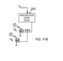
- FIGS. 11A and 11BAn alternate solution disclosed herein provides, as shown in FIGS. 11A and 11B, means for disabling the control circuit on the input side from a condition sensed on the output side of the converter, as described in detail below.
- the principle ideais to short winding N 3 of drive transformer T 3 , detect excessive current in winding N 5 due to shorted winding N 3 , and disable the control circuit and drivers OUTA and OUTB (controller 102 in FIG. 11 A), thus resulting in turn-off the converter.
- Protection logic 200FIG.
- comparator U 6that has a threshold set such that in normal operation the voltage drop across resistor R 12 will not trip U 6 , but when winding N 3 is shorted, comparator U 6 is tripped, and generates signal DSB which disables controller 102 and both OUTA and OUTB are disabled (that is, they are in the low state).
- FIGS. 5A through DAn alternate embodiment disclosed herein provides, as shown in FIGS. 5A through D, a means for disabling the control circuit referenced to the output side of the converter from a condition sensed on the input side of converter as described in detail below.
- Protection logic 201 on the input side of the convertershown in FIGS. 5C and 5D, initially senses a fault condition on the input side and generates a disable signal DSP that is active (high).
- Switch Q 100shown as an n-channel MOSFET as one possible practical realization in FIG. 5C, is connected to one end (either at point “A” or “B”) of winding N 4 (FIG. 5 A).
- transistor Q 100In response to an active disable signal DSP, transistor Q 100 is turned-on and winding N 4 is shorted via Q 100 and diode D 60 , if Q 100 is connected to end “A” of N 4 . Similarly, winding N 4 is shorted via transistor Q 100 and diode D 50 if Q 100 is connected to end “B” of N 4 .
- two primary side switches(specifically Q 20 and Q 30 ), that were on before the DSP signal became active, are turned-off.
- increased current in winding N 3is sensed with resistor R 11 connected between supply voltage V CCS and drivers DRIVER_A and DRIVER_B referenced to the output of the converter. DRIVER_A and DRIVER_B are shown in FIG.
- switch Q 100can be connected in parallel with either primary switch Q 20 or Q 30 in which case the gate of transistor Q 20 or Q 30 will be shorted in response to the active disable signal.
- winding N 4will be shorted via transistor Q 100 and diodes D 20 and D 60 or diodes D 30 and D 50 , causing again increased current through windings N 4 and N 3 .
- a possible drawback of this solutionis that the capacitance of transistor Q 100 may affect the turn-on performance of primary switches Q 20 or Q 30 .
- leakage inductance L 4is needed to be less then L 1 or L 2 , thus resulting in a more complicated drive transformer design.
- the disable circuit from FIG. 5Chas an inherent delay of one switching period since winding N 4 is shorted only during the on-time of either transistors Q 10 and Q 30 or transistors Q 20 and Q 40 . In most applications this should not be a problem.
- two switches shown as n-channel MOSFETs Q 5 and Q 6 in FIG. 5Dare used to short winding N 4 when the DSP signal is high in order to stop controller 104 and disable OUTA and OUTB, immediately, whenever a fault condition on the input side of converter is detected.
- the body diodes of Q 5 and Q 6can replace diodes D 50 and D 60 , respectively, thus further simplifying the circuit.
- this circuitprovides an inherent delay of one half of the switching period.
- winding N 4has the best coupling with winding N 3 , while windings N 2 and N 1 are placed in layers above and below in the PCB. This is the preferred structure because it provides enough leakage between N 3 and N 1 and N 2 , and also decouples N 1 and N 2 from N 3 when N 4 is shorted. Other arrangements of windings in the drive transformer of the invention are also possible.
Landscapes
- Engineering & Computer Science (AREA)
- Power Engineering (AREA)
- Dc-Dc Converters (AREA)
- Power Conversion In General (AREA)
- Control Of Motors That Do Not Use Commutators (AREA)
- Cookers (AREA)
Abstract
Description
Claims (32)
Priority Applications (14)
| Application Number | Priority Date | Filing Date | Title |
|---|---|---|---|
| EP02714806AEP1356575B1 (en) | 2001-02-01 | 2002-02-01 | Isolated drive circuitry used in switch-mode power converters |
| AT02714806TATE361579T1 (en) | 2001-02-01 | 2002-02-01 | ISOLATED DRIVER CIRCUIT ARRANGEMENT FOR USE IN POWER SWITCHING REGULATORS |
| JP2002561353AJP2004521588A (en) | 2001-02-01 | 2002-02-01 | Isolated drive circuit used in switch mode power converter |
| PCT/US2002/002745WO2002061926A2 (en) | 2001-02-01 | 2002-02-01 | Isolated drive circuitry used in switch-mode power converters |
| AU2002247050AAU2002247050A1 (en) | 2001-02-01 | 2002-02-01 | Isolated drive circuitry used in switch-mode power converters |
| DE60224047TDE60224047D1 (en) | 2001-02-01 | 2002-02-01 | INSULATED DRIVER CIRCUIT ARRANGEMENT FOR USE IN CIRCUIT BREAKERS |
| JP2002561354AJP2004536543A (en) | 2001-02-01 | 2002-02-01 | Isolated drive circuit used in switch mode power converter |
| AU2002243742AAU2002243742A1 (en) | 2001-02-01 | 2002-02-01 | Isolated drive circuitry used in switch-mode power converters |
| PCT/US2002/002779WO2002061927A2 (en) | 2001-02-01 | 2002-02-01 | Isolated drive circuitry used in switch-mode power converters |
| DE60219886TDE60219886D1 (en) | 2001-02-01 | 2002-02-01 | INSULATED DRIVER CIRCUIT ARRANGEMENT FOR USE IN CIRCUIT BREAKERS |
| EP02709247AEP1405394B1 (en) | 2001-02-01 | 2002-02-01 | Isolated drive circuitry used in switch-mode power converters |
| AT02709247TATE381141T1 (en) | 2001-02-01 | 2002-02-01 | ISOLATED DRIVER CIRCUIT ARRANGEMENT FOR USE IN POWER SWITCHING REGULATORS |
| US10/061,189US6804125B2 (en) | 2001-02-01 | 2002-02-01 | Isolated drive circuitry used in switch-mode power converters |
| US10/648,659US6791851B2 (en) | 2001-02-01 | 2003-08-26 | Isolated drive circuitry used in switch-mode power converters |
Applications Claiming Priority (2)
| Application Number | Priority Date | Filing Date | Title |
|---|---|---|---|
| US26571401P | 2001-02-01 | 2001-02-01 | |
| US10/061,189US6804125B2 (en) | 2001-02-01 | 2002-02-01 | Isolated drive circuitry used in switch-mode power converters |
Related Child Applications (1)
| Application Number | Title | Priority Date | Filing Date |
|---|---|---|---|
| US10/648,659DivisionUS6791851B2 (en) | 2001-02-01 | 2003-08-26 | Isolated drive circuitry used in switch-mode power converters |
Publications (2)
| Publication Number | Publication Date |
|---|---|
| US20020101741A1 US20020101741A1 (en) | 2002-08-01 |
| US6804125B2true US6804125B2 (en) | 2004-10-12 |
Family
ID=31996451
Family Applications (2)
| Application Number | Title | Priority Date | Filing Date |
|---|---|---|---|
| US10/061,189Expired - LifetimeUS6804125B2 (en) | 2001-02-01 | 2002-02-01 | Isolated drive circuitry used in switch-mode power converters |
| US10/648,659Expired - LifetimeUS6791851B2 (en) | 2001-02-01 | 2003-08-26 | Isolated drive circuitry used in switch-mode power converters |
Family Applications After (1)
| Application Number | Title | Priority Date | Filing Date |
|---|---|---|---|
| US10/648,659Expired - LifetimeUS6791851B2 (en) | 2001-02-01 | 2003-08-26 | Isolated drive circuitry used in switch-mode power converters |
Country Status (7)
| Country | Link |
|---|---|
| US (2) | US6804125B2 (en) |
| EP (2) | EP1356575B1 (en) |
| JP (2) | JP2004521588A (en) |
| AT (2) | ATE381141T1 (en) |
| AU (2) | AU2002243742A1 (en) |
| DE (2) | DE60219886D1 (en) |
| WO (2) | WO2002061926A2 (en) |
Cited By (36)
| Publication number | Priority date | Publication date | Assignee | Title |
|---|---|---|---|---|
| US20050088855A1 (en)* | 2001-12-15 | 2005-04-28 | Thomas Kirchmeier | High frequency excitation system |
| US20060037461A1 (en)* | 2003-08-21 | 2006-02-23 | Masayuki Yasumura | Switching power supply circuit |
| US20070211500A1 (en)* | 2006-03-02 | 2007-09-13 | Hipro Electronic Co., Ltd | DC-DC converter with direct driven synchronous rectifier |
| US7355867B2 (en)* | 2004-08-17 | 2008-04-08 | Elster Electricity, Llc | Power supply for an electric meter having a high-voltage regulator that limits the voltage applied to certain components below the normal operating input voltage |
| US7564702B2 (en)* | 1997-01-24 | 2009-07-21 | Synqor, Inc. | High efficiency power converter |
| US20100164601A1 (en)* | 2008-12-23 | 2010-07-01 | Infineon Technologies Ag | Control circuit for a power semiconductor assembly and power semiconductor assembly |
| US20100188876A1 (en)* | 2009-01-19 | 2010-07-29 | Paul Garrity | Controller for a Power Converter |
| US20100321964A1 (en)* | 2009-06-17 | 2010-12-23 | Antony Brinlee | Power Adapter Employing a Power Reducer |
| US20110019454A1 (en)* | 2007-07-09 | 2011-01-27 | Christopher William Fotherby | Drive Circuit |
| US8023290B2 (en) | 1997-01-24 | 2011-09-20 | Synqor, Inc. | High efficiency power converter |
| US8134443B2 (en) | 2002-04-18 | 2012-03-13 | Flextronics International Usa, Inc. | Extended E matrix integrated magnetics (MIM) core |
| WO2012129485A2 (en) | 2011-03-23 | 2012-09-27 | Power-One, Inc. | Integrated magnetics with isolated drive circuit |
| US8477514B2 (en) | 2006-12-01 | 2013-07-02 | Flextronics International Usa, Inc. | Power system with power converters having an adaptive controller |
| US8488355B2 (en) | 2008-11-14 | 2013-07-16 | Power Systems Technologies, Ltd. | Driver for a synchronous rectifier and power converter employing the same |
| US8502520B2 (en) | 2007-03-14 | 2013-08-06 | Flextronics International Usa, Inc | Isolated power converter |
| US8514593B2 (en) | 2009-06-17 | 2013-08-20 | Power Systems Technologies, Ltd. | Power converter employing a variable switching frequency and a magnetic device with a non-uniform gap |
| US8520420B2 (en) | 2009-12-18 | 2013-08-27 | Power Systems Technologies, Ltd. | Controller for modifying dead time between switches in a power converter |
| US8520414B2 (en) | 2009-01-19 | 2013-08-27 | Power Systems Technologies, Ltd. | Controller for a power converter |
| US8638578B2 (en) | 2009-08-14 | 2014-01-28 | Power System Technologies, Ltd. | Power converter including a charge pump employable in a power adapter |
| US8767418B2 (en) | 2010-03-17 | 2014-07-01 | Power Systems Technologies Ltd. | Control system for a power converter and method of operating the same |
| US8787043B2 (en) | 2010-01-22 | 2014-07-22 | Power Systems Technologies, Ltd. | Controller for a power converter and method of operating the same |
| US8792257B2 (en) | 2011-03-25 | 2014-07-29 | Power Systems Technologies, Ltd. | Power converter with reduced power dissipation |
| US8792256B2 (en) | 2012-01-27 | 2014-07-29 | Power Systems Technologies Ltd. | Controller for a switch and method of operating the same |
| US8976549B2 (en) | 2009-12-03 | 2015-03-10 | Power Systems Technologies, Ltd. | Startup circuit including first and second Schmitt triggers and power converter employing the same |
| US9019061B2 (en) | 2009-03-31 | 2015-04-28 | Power Systems Technologies, Ltd. | Magnetic device formed with U-shaped core pieces and power converter employing the same |
| US9077248B2 (en) | 2009-06-17 | 2015-07-07 | Power Systems Technologies Ltd | Start-up circuit for a power adapter |
| US9099232B2 (en) | 2012-07-16 | 2015-08-04 | Power Systems Technologies Ltd. | Magnetic device and power converter employing the same |
| US9106130B2 (en) | 2012-07-16 | 2015-08-11 | Power Systems Technologies, Inc. | Magnetic device and power converter employing the same |
| US9190898B2 (en) | 2012-07-06 | 2015-11-17 | Power Systems Technologies, Ltd | Controller for a power converter and method of operating the same |
| US9197132B2 (en) | 2006-12-01 | 2015-11-24 | Flextronics International Usa, Inc. | Power converter with an adaptive controller and method of operating the same |
| US9214264B2 (en) | 2012-07-16 | 2015-12-15 | Power Systems Technologies, Ltd. | Magnetic device and power converter employing the same |
| US9240712B2 (en) | 2012-12-13 | 2016-01-19 | Power Systems Technologies Ltd. | Controller including a common current-sense device for power switches of a power converter |
| US9246391B2 (en) | 2010-01-22 | 2016-01-26 | Power Systems Technologies Ltd. | Controller for providing a corrected signal to a sensed peak current through a circuit element of a power converter |
| US9300206B2 (en) | 2013-11-15 | 2016-03-29 | Power Systems Technologies Ltd. | Method for estimating power of a power converter |
| US9379629B2 (en) | 2012-07-16 | 2016-06-28 | Power Systems Technologies, Ltd. | Magnetic device and power converter employing the same |
| US10199950B1 (en) | 2013-07-02 | 2019-02-05 | Vlt, Inc. | Power distribution architecture with series-connected bus converter |
Families Citing this family (16)
| Publication number | Priority date | Publication date | Assignee | Title |
|---|---|---|---|---|
| US6970023B2 (en)* | 2003-12-17 | 2005-11-29 | Texas Instruments Incorporated | Modulated transistor gate driver with planar pulse transformer |
| US6906931B1 (en)* | 2004-01-30 | 2005-06-14 | Astec International Limited | Zero-voltage switching half-bridge DC-DC converter topology by utilizing the transformer leakage inductance trapped energy |
| US7116563B2 (en)* | 2004-05-19 | 2006-10-03 | Semtech Corporation | Dual mode over-current protection for switching mode power converter |
| EP2097920B1 (en)* | 2007-07-23 | 2017-08-09 | TRUMPF Hüttinger GmbH + Co. KG | Plasma supply device |
| US8687386B2 (en)* | 2010-12-06 | 2014-04-01 | The Boeing Company | Synchronous rectifier bi-directional current sensor |
| CN102830740B (en)* | 2012-08-23 | 2014-04-30 | 矽力杰半导体技术(杭州)有限公司 | High-efficiency bias voltage generating circuit |
| GB2511846B (en)* | 2013-03-15 | 2017-07-26 | Eisergy Ltd | A gate drive circuit for a semiconductor switch |
| EP2961049B1 (en) | 2014-06-25 | 2017-04-12 | Siemens Aktiengesellschaft | Control circuit of a resonant converter |
| TWI571055B (en)* | 2015-10-14 | 2017-02-11 | 茂達電子股份有限公司 | Switching driver capable of reducing emi effect and power ripple |
| US10447158B2 (en)* | 2016-07-01 | 2019-10-15 | Texas Instruments Incorporated | Reducing voltage rating of devices in a multilevel converter |
| US9954456B2 (en) | 2016-09-09 | 2018-04-24 | Navitas Semiconductor, Inc. | Flyback converter |
| CN108736698A (en)* | 2017-04-13 | 2018-11-02 | 台达电子工业股份有限公司 | Power supply and residual voltage discharging method |
| GB2567227A (en) | 2017-10-06 | 2019-04-10 | Heyday Integrated Circuits | Galvanically isolated gate drive circuit with power transfer |
| US12027845B2 (en)* | 2020-02-19 | 2024-07-02 | Aerojet Rocketdyne, Inc. | Shoot through current detection and protection circuit |
| CN113315355B (en)* | 2021-07-02 | 2022-12-13 | 上海空间电源研究所 | High-reliability delay isolation driving circuit for spacecraft |
| US12267071B2 (en) | 2023-06-01 | 2025-04-01 | Allegro Microsystems, Llc | Desaturation circuit having temperature compensation |
Citations (24)
| Publication number | Priority date | Publication date | Assignee | Title |
|---|---|---|---|---|
| JPS58136137A (en) | 1982-02-08 | 1983-08-13 | Hitachi Ltd | Control circuit for field effect transistor |
| US4591964A (en) | 1982-02-05 | 1986-05-27 | Telefonaktiebolaget Lm Ericsson | Method of securely interrupting the electric power supply from a low-frequency or direct voltage source to a load, and appartus for carrying out the method |
| US4884186A (en) | 1987-12-10 | 1989-11-28 | Boschert Incorporated | Power supply with reduced switching losses |
| JPH03128673A (en) | 1989-10-12 | 1991-05-31 | Koufu Nippon Denki Kk | Dc-dc converter |
| DE4035969A1 (en) | 1990-01-26 | 1991-08-01 | Siemens Ag | CIRCUIT ARRANGEMENT WITH AT LEAST ONE SWITCHING DEVICE CONTAINING A POWER MOSFET |
| US5198969A (en) | 1990-07-13 | 1993-03-30 | Design Automation, Inc. | Soft-switching full-bridge dc/dc converting |
| WO1993019516A1 (en) | 1992-03-25 | 1993-09-30 | Raynet Corporation | Dc/dc/ac power supply |
| US5274543A (en) | 1992-04-20 | 1993-12-28 | At&T Bell Laboratories | Zero-voltage switching power converter with lossless synchronous rectifier gate drive |
| US5353212A (en) | 1992-04-20 | 1994-10-04 | At&T Bell Laboratories | Zero-voltage switching power converter with ripple current cancellation |
| DE4327073C1 (en) | 1993-08-12 | 1994-10-13 | Knick Elektronische Mesgeraete | Chopper circuit for DC-isolated transmission of bipolar measurement currents |
| US5590032A (en) | 1995-05-25 | 1996-12-31 | Lucent Technologies Inc. | Self-synchronized drive circuit for a synchronous rectifier in a clamped-mode power converter |
| US5726869A (en) | 1995-10-05 | 1998-03-10 | Fujitsu Limited | Synchronous rectifier type DC-to-DC converter in which a saturable inductive device is connected in series with a secondary-side switching device |
| JPH10215584A (en) | 1997-01-28 | 1998-08-11 | Matsushita Electric Works Ltd | Power supply |
| US5870299A (en) | 1997-05-28 | 1999-02-09 | Lucent Technologies Inc. | Method and apparatus for damping ringing in self-driven synchronous rectifiers |
| US5880939A (en) | 1996-09-06 | 1999-03-09 | Sinfor | Stabilized power supply circuit including hyperresonant chopping and synchronous rectification |
| US5907481A (en) | 1997-10-31 | 1999-05-25 | Telefonaktiebolaget Lm Ericsson | Double ended isolated D.C.--D.C. converter |
| EP0957568A2 (en) | 1998-04-16 | 1999-11-17 | Sony Corporation | Current resonance type switching power source |
| US5999432A (en)* | 1985-06-04 | 1999-12-07 | Nilssen; Ole K. | High-efficiency bridge inverter |
| US6038148A (en) | 1998-12-11 | 2000-03-14 | Ericsson, Inc. | Self-driven synchronous rectification scheme |
| US6069802A (en) | 1998-07-31 | 2000-05-30 | Priegnitz; Robert A. | Transformer isolated driver and isolated forward converter |
| US6111769A (en) | 1999-09-24 | 2000-08-29 | Ericsson, Inc. | External driving circuit for bridge type synchronous rectification |
| US6169683B1 (en)* | 1999-10-07 | 2001-01-02 | Ericsson Inc. | Resonant gate drive for synchronous rectifiers |
| US6185114B1 (en) | 1999-03-05 | 2001-02-06 | Murata Manufacturing Co., Ltd. | Isolating DC-DC converter |
| US6504739B2 (en)* | 2001-05-18 | 2003-01-07 | Astec International Limited | Simple control circuit for synchronous rectifiers used in ZVS phase shifted full bridge converter |
Family Cites Families (2)
| Publication number | Priority date | Publication date | Assignee | Title |
|---|---|---|---|---|
| JP3030672B2 (en)* | 1991-06-18 | 2000-04-10 | 和光純薬工業株式会社 | New resist material and pattern forming method |
| US5499184A (en)* | 1994-01-28 | 1996-03-12 | Compaq Computer Corp. | Power switch circuitry for electrically isolating the power switch from a power supply |
- 2002
- 2002-02-01ATAT02709247Tpatent/ATE381141T1/ennot_activeIP Right Cessation
- 2002-02-01ATAT02714806Tpatent/ATE361579T1/ennot_activeIP Right Cessation
- 2002-02-01JPJP2002561353Apatent/JP2004521588A/enactivePending
- 2002-02-01AUAU2002243742Apatent/AU2002243742A1/ennot_activeAbandoned
- 2002-02-01JPJP2002561354Apatent/JP2004536543A/enactivePending
- 2002-02-01AUAU2002247050Apatent/AU2002247050A1/ennot_activeAbandoned
- 2002-02-01DEDE60219886Tpatent/DE60219886D1/ennot_activeExpired - Lifetime
- 2002-02-01DEDE60224047Tpatent/DE60224047D1/ennot_activeExpired - Lifetime
- 2002-02-01EPEP02714806Apatent/EP1356575B1/ennot_activeExpired - Lifetime
- 2002-02-01WOPCT/US2002/002745patent/WO2002061926A2/enactiveIP Right Grant
- 2002-02-01USUS10/061,189patent/US6804125B2/ennot_activeExpired - Lifetime
- 2002-02-01WOPCT/US2002/002779patent/WO2002061927A2/enactiveIP Right Grant
- 2002-02-01EPEP02709247Apatent/EP1405394B1/ennot_activeExpired - Lifetime
- 2003
- 2003-08-26USUS10/648,659patent/US6791851B2/ennot_activeExpired - Lifetime
Patent Citations (25)
| Publication number | Priority date | Publication date | Assignee | Title |
|---|---|---|---|---|
| US4591964A (en) | 1982-02-05 | 1986-05-27 | Telefonaktiebolaget Lm Ericsson | Method of securely interrupting the electric power supply from a low-frequency or direct voltage source to a load, and appartus for carrying out the method |
| JPS58136137A (en) | 1982-02-08 | 1983-08-13 | Hitachi Ltd | Control circuit for field effect transistor |
| US5999432A (en)* | 1985-06-04 | 1999-12-07 | Nilssen; Ole K. | High-efficiency bridge inverter |
| US4884186A (en) | 1987-12-10 | 1989-11-28 | Boschert Incorporated | Power supply with reduced switching losses |
| JPH03128673A (en) | 1989-10-12 | 1991-05-31 | Koufu Nippon Denki Kk | Dc-dc converter |
| DE4035969A1 (en) | 1990-01-26 | 1991-08-01 | Siemens Ag | CIRCUIT ARRANGEMENT WITH AT LEAST ONE SWITCHING DEVICE CONTAINING A POWER MOSFET |
| US5198969A (en) | 1990-07-13 | 1993-03-30 | Design Automation, Inc. | Soft-switching full-bridge dc/dc converting |
| WO1993019516A1 (en) | 1992-03-25 | 1993-09-30 | Raynet Corporation | Dc/dc/ac power supply |
| US5353212A (en) | 1992-04-20 | 1994-10-04 | At&T Bell Laboratories | Zero-voltage switching power converter with ripple current cancellation |
| US5274543A (en) | 1992-04-20 | 1993-12-28 | At&T Bell Laboratories | Zero-voltage switching power converter with lossless synchronous rectifier gate drive |
| DE4327073C1 (en) | 1993-08-12 | 1994-10-13 | Knick Elektronische Mesgeraete | Chopper circuit for DC-isolated transmission of bipolar measurement currents |
| US5590032A (en) | 1995-05-25 | 1996-12-31 | Lucent Technologies Inc. | Self-synchronized drive circuit for a synchronous rectifier in a clamped-mode power converter |
| USRE37510E1 (en) | 1995-05-25 | 2002-01-15 | Lucent Technologies Inc. | Self-synchronized drive circuit for a synchronized rectifier in a clamped-mode power converter |
| US5726869A (en) | 1995-10-05 | 1998-03-10 | Fujitsu Limited | Synchronous rectifier type DC-to-DC converter in which a saturable inductive device is connected in series with a secondary-side switching device |
| US5880939A (en) | 1996-09-06 | 1999-03-09 | Sinfor | Stabilized power supply circuit including hyperresonant chopping and synchronous rectification |
| JPH10215584A (en) | 1997-01-28 | 1998-08-11 | Matsushita Electric Works Ltd | Power supply |
| US5870299A (en) | 1997-05-28 | 1999-02-09 | Lucent Technologies Inc. | Method and apparatus for damping ringing in self-driven synchronous rectifiers |
| US5907481A (en) | 1997-10-31 | 1999-05-25 | Telefonaktiebolaget Lm Ericsson | Double ended isolated D.C.--D.C. converter |
| EP0957568A2 (en) | 1998-04-16 | 1999-11-17 | Sony Corporation | Current resonance type switching power source |
| US6069802A (en) | 1998-07-31 | 2000-05-30 | Priegnitz; Robert A. | Transformer isolated driver and isolated forward converter |
| US6038148A (en) | 1998-12-11 | 2000-03-14 | Ericsson, Inc. | Self-driven synchronous rectification scheme |
| US6185114B1 (en) | 1999-03-05 | 2001-02-06 | Murata Manufacturing Co., Ltd. | Isolating DC-DC converter |
| US6111769A (en) | 1999-09-24 | 2000-08-29 | Ericsson, Inc. | External driving circuit for bridge type synchronous rectification |
| US6169683B1 (en)* | 1999-10-07 | 2001-01-02 | Ericsson Inc. | Resonant gate drive for synchronous rectifiers |
| US6504739B2 (en)* | 2001-05-18 | 2003-01-07 | Astec International Limited | Simple control circuit for synchronous rectifiers used in ZVS phase shifted full bridge converter |
Cited By (53)
| Publication number | Priority date | Publication date | Assignee | Title |
|---|---|---|---|---|
| US8493751B2 (en) | 1997-01-24 | 2013-07-23 | Synqor, Inc. | High efficiency power converter |
| US9143042B2 (en) | 1997-01-24 | 2015-09-22 | Synqor, Inc. | High efficiency power converter |
| US8023290B2 (en) | 1997-01-24 | 2011-09-20 | Synqor, Inc. | High efficiency power converter |
| US7564702B2 (en)* | 1997-01-24 | 2009-07-21 | Synqor, Inc. | High efficiency power converter |
| US7161818B2 (en)* | 2001-12-15 | 2007-01-09 | Huttinger Elektronik Gmbh + Co. Kg | High frequency excitation system |
| US20070085133A1 (en)* | 2001-12-15 | 2007-04-19 | Huettinger Elektronik Gmbh + Co. Kg | High frequency excitation system |
| US20050088855A1 (en)* | 2001-12-15 | 2005-04-28 | Thomas Kirchmeier | High frequency excitation system |
| US7440301B2 (en) | 2001-12-15 | 2008-10-21 | Huettinger Elektronik Gmbh & Co. Kg | High frequency excitation system |
| US20090015314A1 (en)* | 2001-12-15 | 2009-01-15 | Huettinger Elektronik Gmbh + Co. Kg | High frequency excitation system |
| US7652901B2 (en) | 2001-12-15 | 2010-01-26 | Huettinger Elektronik Gmbh + Co. Kg | High frequency excitation system |
| US8134443B2 (en) | 2002-04-18 | 2012-03-13 | Flextronics International Usa, Inc. | Extended E matrix integrated magnetics (MIM) core |
| US7167384B2 (en)* | 2003-08-21 | 2007-01-23 | Sony Corporation | Switching power circuit |
| US20060037461A1 (en)* | 2003-08-21 | 2006-02-23 | Masayuki Yasumura | Switching power supply circuit |
| US7355867B2 (en)* | 2004-08-17 | 2008-04-08 | Elster Electricity, Llc | Power supply for an electric meter having a high-voltage regulator that limits the voltage applied to certain components below the normal operating input voltage |
| US20070211500A1 (en)* | 2006-03-02 | 2007-09-13 | Hipro Electronic Co., Ltd | DC-DC converter with direct driven synchronous rectifier |
| US9197132B2 (en) | 2006-12-01 | 2015-11-24 | Flextronics International Usa, Inc. | Power converter with an adaptive controller and method of operating the same |
| US8477514B2 (en) | 2006-12-01 | 2013-07-02 | Flextronics International Usa, Inc. | Power system with power converters having an adaptive controller |
| US8502520B2 (en) | 2007-03-14 | 2013-08-06 | Flextronics International Usa, Inc | Isolated power converter |
| US20110019454A1 (en)* | 2007-07-09 | 2011-01-27 | Christopher William Fotherby | Drive Circuit |
| US8526206B2 (en)* | 2007-07-09 | 2013-09-03 | Power Concepts Nz Limited | Drive circuit |
| US8488355B2 (en) | 2008-11-14 | 2013-07-16 | Power Systems Technologies, Ltd. | Driver for a synchronous rectifier and power converter employing the same |
| US7969208B2 (en)* | 2008-12-23 | 2011-06-28 | Infineon Technologies Ag | Control circuit for a power semiconductor assembly and power semiconductor assembly |
| US20100164601A1 (en)* | 2008-12-23 | 2010-07-01 | Infineon Technologies Ag | Control circuit for a power semiconductor assembly and power semiconductor assembly |
| US8520414B2 (en) | 2009-01-19 | 2013-08-27 | Power Systems Technologies, Ltd. | Controller for a power converter |
| US20100188876A1 (en)* | 2009-01-19 | 2010-07-29 | Paul Garrity | Controller for a Power Converter |
| US9088216B2 (en) | 2009-01-19 | 2015-07-21 | Power Systems Technologies, Ltd. | Controller for a synchronous rectifier switch |
| US9019061B2 (en) | 2009-03-31 | 2015-04-28 | Power Systems Technologies, Ltd. | Magnetic device formed with U-shaped core pieces and power converter employing the same |
| US8514593B2 (en) | 2009-06-17 | 2013-08-20 | Power Systems Technologies, Ltd. | Power converter employing a variable switching frequency and a magnetic device with a non-uniform gap |
| US8643222B2 (en) | 2009-06-17 | 2014-02-04 | Power Systems Technologies Ltd | Power adapter employing a power reducer |
| US20100321964A1 (en)* | 2009-06-17 | 2010-12-23 | Antony Brinlee | Power Adapter Employing a Power Reducer |
| US9077248B2 (en) | 2009-06-17 | 2015-07-07 | Power Systems Technologies Ltd | Start-up circuit for a power adapter |
| US8638578B2 (en) | 2009-08-14 | 2014-01-28 | Power System Technologies, Ltd. | Power converter including a charge pump employable in a power adapter |
| US8976549B2 (en) | 2009-12-03 | 2015-03-10 | Power Systems Technologies, Ltd. | Startup circuit including first and second Schmitt triggers and power converter employing the same |
| US8520420B2 (en) | 2009-12-18 | 2013-08-27 | Power Systems Technologies, Ltd. | Controller for modifying dead time between switches in a power converter |
| US8787043B2 (en) | 2010-01-22 | 2014-07-22 | Power Systems Technologies, Ltd. | Controller for a power converter and method of operating the same |
| US9246391B2 (en) | 2010-01-22 | 2016-01-26 | Power Systems Technologies Ltd. | Controller for providing a corrected signal to a sensed peak current through a circuit element of a power converter |
| US8767418B2 (en) | 2010-03-17 | 2014-07-01 | Power Systems Technologies Ltd. | Control system for a power converter and method of operating the same |
| US8929103B2 (en) | 2011-03-23 | 2015-01-06 | Pai Capital Llc | Integrated magnetics with isolated drive circuit |
| WO2012129485A2 (en) | 2011-03-23 | 2012-09-27 | Power-One, Inc. | Integrated magnetics with isolated drive circuit |
| US8792257B2 (en) | 2011-03-25 | 2014-07-29 | Power Systems Technologies, Ltd. | Power converter with reduced power dissipation |
| US8792256B2 (en) | 2012-01-27 | 2014-07-29 | Power Systems Technologies Ltd. | Controller for a switch and method of operating the same |
| US9190898B2 (en) | 2012-07-06 | 2015-11-17 | Power Systems Technologies, Ltd | Controller for a power converter and method of operating the same |
| US9379629B2 (en) | 2012-07-16 | 2016-06-28 | Power Systems Technologies, Ltd. | Magnetic device and power converter employing the same |
| US9099232B2 (en) | 2012-07-16 | 2015-08-04 | Power Systems Technologies Ltd. | Magnetic device and power converter employing the same |
| US9214264B2 (en) | 2012-07-16 | 2015-12-15 | Power Systems Technologies, Ltd. | Magnetic device and power converter employing the same |
| US9106130B2 (en) | 2012-07-16 | 2015-08-11 | Power Systems Technologies, Inc. | Magnetic device and power converter employing the same |
| US9240712B2 (en) | 2012-12-13 | 2016-01-19 | Power Systems Technologies Ltd. | Controller including a common current-sense device for power switches of a power converter |
| US10594223B1 (en) | 2013-07-02 | 2020-03-17 | Vlt, Inc. | Power distribution architecture with series-connected bus converter |
| US10199950B1 (en) | 2013-07-02 | 2019-02-05 | Vlt, Inc. | Power distribution architecture with series-connected bus converter |
| US11075583B1 (en) | 2013-07-02 | 2021-07-27 | Vicor Corporation | Power distribution architecture with series-connected bus converter |
| US11705820B2 (en) | 2013-07-02 | 2023-07-18 | Vicor Corporation | Power distribution architecture with series-connected bus converter |
| US12395087B1 (en) | 2013-07-02 | 2025-08-19 | Vicor Corporation | Power distribution architecture with series-connected bus converter |
| US9300206B2 (en) | 2013-11-15 | 2016-03-29 | Power Systems Technologies Ltd. | Method for estimating power of a power converter |
Also Published As
| Publication number | Publication date |
|---|---|
| DE60224047D1 (en) | 2008-01-24 |
| WO2002061927A3 (en) | 2004-02-12 |
| US6791851B2 (en) | 2004-09-14 |
| AU2002247050A8 (en) | 2002-08-12 |
| US20020101741A1 (en) | 2002-08-01 |
| JP2004536543A (en) | 2004-12-02 |
| WO2002061926A3 (en) | 2003-08-14 |
| AU2002243742A1 (en) | 2002-08-12 |
| ATE381141T1 (en) | 2007-12-15 |
| EP1356575B1 (en) | 2007-05-02 |
| US20040047164A1 (en) | 2004-03-11 |
| DE60219886D1 (en) | 2007-06-14 |
| EP1405394A2 (en) | 2004-04-07 |
| JP2004521588A (en) | 2004-07-15 |
| WO2002061926A2 (en) | 2002-08-08 |
| EP1356575A2 (en) | 2003-10-29 |
| EP1405394B1 (en) | 2007-12-12 |
| WO2002061927A2 (en) | 2002-08-08 |
| ATE361579T1 (en) | 2007-05-15 |
| AU2002247050A1 (en) | 2002-08-12 |
Similar Documents
| Publication | Publication Date | Title |
|---|---|---|
| US6804125B2 (en) | Isolated drive circuitry used in switch-mode power converters | |
| US7102898B2 (en) | Isolated drive circuitry used in switch-mode power converters | |
| US6822882B1 (en) | Gate driver with a DC offset bias circuit and a power converter employing the same | |
| US4864479A (en) | Full-bridge lossless switching converter | |
| US5351179A (en) | Lossless active snubber for half-bridge output rectifiers | |
| US6031747A (en) | Interleaved synchronous flyback converter with high efficiency over a wide operating load range | |
| US6069803A (en) | Offset resonance zero volt switching flyback converter | |
| US9991805B2 (en) | On and off controlled resonant DC-DC power converter | |
| US6882548B1 (en) | Auxiliary active clamp circuit, a method of clamping a voltage of a rectifier switch and a power converter employing the circuit or method | |
| US6483724B1 (en) | DC/DC ZVS full bridge converter power supply method and apparatus | |
| US5539630A (en) | Soft-switching converter DC-to-DC isolated with voltage bidirectional switches on the secondary side of an isolation transformer | |
| US5438498A (en) | Series resonant converter having a resonant snubber | |
| US7738266B2 (en) | Forward power converter controllers | |
| US6061255A (en) | Drive circuit for synchronous rectifiers in isolated forward converter | |
| EP3509203B1 (en) | Converter with zvs | |
| US5822199A (en) | Controller for a power switch and method of operation thereof | |
| US8817497B2 (en) | Switching power converter for reducing EMI from ring oscillation and its control method | |
| EP1495531A1 (en) | High efficiency flyback converter | |
| JP2004536543A5 (en) | ||
| JP2017508437A (en) | Adaptive synchronous switching in resonant converters. | |
| CN101102086B (en) | switch drive circuit | |
| KR102652342B1 (en) | High performance two stage power converter with enhanced light load management | |
| US5986904A (en) | Self-regulating lossless snubber circuit | |
| JP2000004584A (en) | Dc-to-dc power converter | |
| US6417629B1 (en) | Push-pull based voltage-clamping electronic ballast |
Legal Events
| Date | Code | Title | Description |
|---|---|---|---|
| AS | Assignment | Owner name:DI/DT INC., CALIFORNIA Free format text:ASSIGNMENT OF ASSIGNORS INTEREST;ASSIGNOR:BRKOVIC, MILIVOJE S.;REEL/FRAME:012555/0934 Effective date:20020131 | |
| STCF | Information on status: patent grant | Free format text:PATENTED CASE | |
| AS | Assignment | Owner name:POWER-ONE, INC., CALIFORNIA Free format text:ASSIGNMENT OF ASSIGNORS INTEREST;ASSIGNOR:DI/DT, INC.;REEL/FRAME:017366/0569 Effective date:20051206 | |
| AS | Assignment | Owner name:PWER BRIDGE, LLC, ALASKA Free format text:SECURITY AGREEMENT;ASSIGNOR:POWER-ONE, INC.;REEL/FRAME:020617/0177 Effective date:20080306 Owner name:PWER BRIDGE, LLC,ALASKA Free format text:SECURITY AGREEMENT;ASSIGNOR:POWER-ONE, INC.;REEL/FRAME:020617/0177 Effective date:20080306 | |
| AS | Assignment | Owner name:PWER BRIDGE, LLC, ARKANSAS Free format text:CORRECTIV;ASSIGNOR:POWER-ONE, INC.;REEL/FRAME:020741/0403 Effective date:20080306 Owner name:PWER BRIDGE, LLC,ARKANSAS Free format text:CORRECTIVE ASSIGNMENT TO CORRECT THE ASSIGNEE ADDR;ASSIGNOR:POWER-ONE, INC.;REEL/FRAME:020741/0403 Effective date:20080306 Owner name:PWER BRIDGE, LLC, ARKANSAS Free format text:CORRECTIVE ASSIGNMENT TO CORRECT THE ASSIGNEE ADDR;ASSIGNOR:POWER-ONE, INC.;REEL/FRAME:020741/0403 Effective date:20080306 | |
| FPAY | Fee payment | Year of fee payment:4 | |
| AS | Assignment | Owner name:POWER-ONE, INC., CALIFORNIA Free format text:RELEASE BY SECURED PARTY;ASSIGNOR:PWER BRIDGE, LLC;REEL/FRAME:021253/0024 Effective date:20080617 Owner name:THE BANK OF NEW YORK TRUST COMPANY, N.A., CALIFORN Free format text:SECURITY AGREEMENT;ASSIGNOR:POWER-ONE, INC.;REEL/FRAME:021253/0076 Effective date:20080617 Owner name:POWER-ONE, INC.,CALIFORNIA Free format text:RELEASE BY SECURED PARTY;ASSIGNOR:PWER BRIDGE, LLC;REEL/FRAME:021253/0024 Effective date:20080617 Owner name:THE BANK OF NEW YORK TRUST COMPANY, N.A.,CALIFORNI Free format text:SECURITY AGREEMENT;ASSIGNOR:POWER-ONE, INC.;REEL/FRAME:021253/0076 Effective date:20080617 | |
| AS | Assignment | Owner name:POWER-ONE, INC., CALIFORNIA Free format text:RELEASE BY SECURED PARTY;ASSIGNOR:THE BANK OF NEW YORK MELLON TRUST COMPANY, N.A. (AS SUCCESSOR TO THE BANK OF NEW YORK TRUST COMPANY, N.A.);REEL/FRAME:026026/0794 Effective date:20110317 | |
| AS | Assignment | Owner name:BANK OF AMERICA, N.A., WASHINGTON Free format text:SECURITY AGREEMENT;ASSIGNOR:POWER-ONE, INC.;REEL/FRAME:026401/0098 Effective date:20110329 | |
| FPAY | Fee payment | Year of fee payment:8 | |
| AS | Assignment | Owner name:POWER-ONE, INC., CALIFORNIA Free format text:RELEASE BY SECURED PARTY;ASSIGNOR:BANK OF AMERICA, N.A. AS ADMINISTRATIVE AGENT;REEL/FRAME:032826/0684 Effective date:20130722 | |
| AS | Assignment | Owner name:PAI CAPITAL LLC, CALIFORNIA Free format text:NUNC PRO TUNC ASSIGNMENT;ASSIGNOR:POWER-ONE, INC.;REEL/FRAME:033227/0968 Effective date:20140604 | |
| FPAY | Fee payment | Year of fee payment:12 | |
| AS | Assignment | Owner name:BEL POWER SOLUTIONS INC., CALIFORNIA Free format text:ASSIGNMENT OF ASSIGNORS INTEREST;ASSIGNOR:PAI CAPITAL LLC;REEL/FRAME:043086/0433 Effective date:20170615 | |
| AS | Assignment | Owner name:KEYBANK NATIONAL ASSOCIATION, AS ADMINISTRATIVE AGENT, OHIO Free format text:SECURITY INTEREST;ASSIGNOR:BEL FUSE INC.;REEL/FRAME:058917/0452 Effective date:20210902 |