US6803680B2 - Apparatus, methods, and articles of manufacture for a switch having sharpened control voltage - Google Patents
Apparatus, methods, and articles of manufacture for a switch having sharpened control voltageDownload PDFInfo
- Publication number
- US6803680B2 US6803680B2US10/390,957US39095703AUS6803680B2US 6803680 B2US6803680 B2US 6803680B2US 39095703 AUS39095703 AUS 39095703AUS 6803680 B2US6803680 B2US 6803680B2
- Authority
- US
- United States
- Prior art keywords
- switch
- fets
- fet
- gate
- coupled
- Prior art date
- Legal status (The legal status is an assumption and is not a legal conclusion. Google has not performed a legal analysis and makes no representation as to the accuracy of the status listed.)
- Expired - Lifetime
Links
Images


Classifications
- H—ELECTRICITY
- H03—ELECTRONIC CIRCUITRY
- H03K—PULSE TECHNIQUE
- H03K17/00—Electronic switching or gating, i.e. not by contact-making and –breaking
- H03K17/10—Modifications for increasing the maximum permissible switched voltage
- H03K17/102—Modifications for increasing the maximum permissible switched voltage in field-effect transistor switches
- H—ELECTRICITY
- H10—SEMICONDUCTOR DEVICES; ELECTRIC SOLID-STATE DEVICES NOT OTHERWISE PROVIDED FOR
- H10D—INORGANIC ELECTRIC SEMICONDUCTOR DEVICES
- H10D84/00—Integrated devices formed in or on semiconductor substrates that comprise only semiconducting layers, e.g. on Si wafers or on GaAs-on-Si wafers
- H10D84/80—Integrated devices formed in or on semiconductor substrates that comprise only semiconducting layers, e.g. on Si wafers or on GaAs-on-Si wafers characterised by the integration of at least one component covered by groups H10D12/00 or H10D30/00, e.g. integration of IGFETs
- H10D84/811—Combinations of field-effect devices and one or more diodes, capacitors or resistors
- H—ELECTRICITY
- H10—SEMICONDUCTOR DEVICES; ELECTRIC SOLID-STATE DEVICES NOT OTHERWISE PROVIDED FOR
- H10D—INORGANIC ELECTRIC SEMICONDUCTOR DEVICES
- H10D89/00—Aspects of integrated devices not covered by groups H10D84/00 - H10D88/00
Definitions
- the present inventionrelates generally to switch devices, and more particularly to solid-state switch devices.
- switch devicesoperate to control the path on which a signal travels.
- electromechanical and solid stateAll switches are considered active devices, in that some sort of power supply is required in order to function properly.
- electromechanical switchesa contact is provided that physically changes position during the switching process.
- Solid-state switchesdo not contain any moving parts and instead use some kind of semiconductor device for the switching process, which are basically either diodes or transistors.
- diode switchessense current as a control input while switches comprised of transistors sense voltages as control inputs.
- One example of a transistor-based switchis comprised of a plurality of field effect transistors (FETs).
- FET switchesare generally known to be utilized in connection with high frequency signal transmission, for example, radio frequency (RF).
- RFradio frequency
- a FET switchIn general, a FET switch is in an ON state (very low resistance) allowing any signal to pass from the drain to the source of the FET until a control voltage of a predefined amount (pinch-off voltage) is applied to the gate of the FET. When the pinch-off voltage is applied, the FET switches to an OFF state (very high resistance) and prevents any signal passing from the drain to the source of the FET.
- the advantage of FET switchis that the control voltage applied to the gate of the FET draws very little current, consuming no power in performing the switching function.
- a major drawback of FET switchesis that in the OFF state, a signal that one may desire to prevent from passing through the FET from the drain to the source applies a voltage at the drain of the FET. This voltage travels through the FET to the gate and adds to the control voltage input. As this voltage becomes greater than the control voltage, the OFF state FET begins to turn ON as shown in the FIG. 1 .
- FIG. 2reduces the control voltage needed, but increases the resistance in the ON state. To overcome this added resistance, each FET is made larger and thus an increase in die size for the switch is required. This size increase, however, introduces many new problems in the switch, including:
- the switchcosts more, requiring more semiconductor material to manufacture.
- the switchhas poorer isolation, providing less resistance in the OFF state.
- the switchhas greater leakage in the control line, requiring more power to control the switch
- a switchincludes a plurality of field effect transistors (FETs) with a bypass resistance topology coupled across the FETs so as to be in parallel with the FETs.
- the bypass resistance topologyis used to sharpen the control voltage of the switch.
- the bypass resistance topologyincludes a resistive element coupled across the entire switch (all of the FETs).
- a separate resistive elementis coupled across each FET.
- the switchmay include any number of FETs and have any number of gates.
- the switchmay use a single-gate FET architecture, a multi-gate FET architecture, or a mixed gate architecture.
- the apparatusmay also utilize a plurality of parallel switches that are each connected to the same source voltage.
- a switchutilizes a plurality of FETs having a total of six gates to allow the switch to operate at a low control voltage without the need to increase device periphery or die size.
- the switchmay include a single-gate FET architecture, a multi-gate FET architecture, or a mixed gate architecture, as long as the total number of gates in the switch equals six.
- a switchincludes feed-forward capacitors.
- the feed-forward capacitorsreduce signal distortion and improve the linearity and harmonic noise rejection characteristics of the FETs within the switch and thus lowers the harmonics of the switch.
- the switchincludes two feed-forward capacitors. A first feed-forward capacitor connected between the gate and source of an uppermost FET and the second feed-forward capacitor connected between the gate and drain of a lowermost FET
- a switchincludes a gate resistance topology connected between the gates and a control voltage.
- the gate resistance topologyis used to minimize the effects of leakage current and reduce the resistor voltage drop for process points where FET diode leakage is an issue.
- FIG. 1 ais an exemplary embodiment illustrating the operation of a prior art FET
- FIG. 1 bis another exemplary embodiment illustrating the operation of a prior art FET
- FIG. 2illustrates an exemplary schematic diagram of a switch, according to one embodiment of the present invention
- FIG. 3illustrates an exemplary schematic diagram of a six-gate switch, according to one embodiment of the present invention
- FIG. 4 aillustrates an exemplary schematic diagram of a switch having a single bypass resistor, according to one embodiment of the present invention
- FIG. 4 billustrates an exemplary schematic diagram of a single-gate switch having multi-bypass resistors, according to one embodiment of the present invention
- FIG. 4 cillustrates an exemplary schematic diagram of a dual-gate switch having multi-bypass resistors, according to one embodiment of the present invention
- FIG. 5illustrates an exemplary schematic diagram of a switch having feed-forward capacitors, according to one embodiment of the present invention
- FIG. 6 aillustrates an exemplary schematic diagram of a switch having a gate resistance topology, according to one embodiment of the present invention
- FIG. 6 billustrates an exemplary schematic diagram of a switch having a gate resistance topology, according to one embodiment of the present invention
- FIG. 6 cillustrates an exemplary schematic diagram of a switch having a gate resistance topology, according to one embodiment of the present invention
- FIG. 6 dillustrates an exemplary schematic diagram of a switch having a gate resistance topology, according to one embodiment of the present invention
- FIG. 6 eillustrates an exemplary schematic diagram of a switch having a gate resistance topology, according to one embodiment of the present invention
- FIG. 6 fillustrates an exemplary schematic diagram of a switch having a gate resistance topology, according to one embodiment of the present invention
- FIG. 7illustrates an exemplary schematic diagram of a device having multiple switches in parallel, according to one embodiment of the present invention
- FIG. 8illustrates an exemplary schematic diagram of a device having multiple switches in parallel, according to one embodiment of the present invention
- FIGS. 9-9Dillustrates an exemplary chip layout design having a plurality of switches, according to one embodiment of the present invention.
- FIGS. 10-10Billustrates an exemplary chip layout design having a plurality of switches, according to one embodiment of the present invention.
- FIGS. 11-11Iillustrates an exemplary chip layout design having a plurality of switches, according to one embodiment of the present invention.
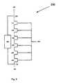
- FIG. 2illustrates an exemplary schematic diagram of a switch 100 , according to one embodiment of the present invention.
- the switch 100includes a plurality of field effect transistors (FETs) 110 , 115 , 120 , 125 , and 130 connected together in series.
- Each FEThas a source 110 S- 130 S, a gate 110 G- 130 G, and a drain 110 D- 130 D.
- the drain of one FETis connected to the source of the next FET (i.e., drain 110 D is connected to source 115 S).
- the source 110 S of the first FET 110is connected to a source voltage input 142 that provides a source voltage for the switch 100 .
- Each of the gates 110 G- 130 Gare coupled together and connected to a control voltage input 145 that provides a control voltage.
- the drain 130 D of the last FET 130is connected to an output 150 that will provide an output (i.e., current) to a load.
- the switch 100also includes a bypass resistance topology 160 coupled between the source voltage input 142 (first source 110 S) and the output 150 (last drain 130 D) so as to be coupled across (in parallel to) each of the FETs.
- bypass resistance topology 160provides no output until the pinch-off voltage is attained.
- the switchdoes not have a precise turn on time and instead starts to turn on prior to the pinch-off voltage being applied (see 1130 of FIG. 1 ).
- the use of the bypass resistance topology 160 in parallel to the FETsincreases the precision timing of the switch activation (i.e., sharpen the control voltage).
- the bypass resistance topology 160provides a known resistive path between the source voltage input 142 and the output 150 (in parallel to the FETs).
- the bypass resistance topology 160has a resistance that is less than the resistance of the FETs in an OFF state (theoretically infinite) but more that the FETs in an ON state. The selection of the resistance in this range allows the bypass resistance topology 160 to control the flow of current.
- the bypass resistance topology 160When the switch is in an OFF state, the bypass resistance topology 160 produces a known current flow (in effect a known leakage current) through that path. As the control voltage is increased towards the pinch-off voltage, the resistance of the FET starts to be reduced. This reduction in resistance of the FET would normally lead to increased leakage current or partial switch activation prior to the pinch-off current being reached. However, the bypass resistance topology 160 limits (and ideally prevents) the current from flowing through the FETs until a point when the resistance of the FETs is less that the resistance of the bypass resistance topology 160 . In effect, the bypass resistance topology 160 is limiting (or preventing) current from flowing through the FETs until the FETs are closer to reaching the pinch-off voltage and turning ON. Thus, the bypass resistance topology 160 increases the precision timing of switch activation by sharpening the control voltage.
- the bypass resistance topology 160is coupled between the source voltage input 142 and the output so as to be in parallel with all of the FETs.
- the present embodimentis not limited thereto, as will be evident by various embodiments disclosed later with regard to FIGS. 4 a - 3 c .
- the switch 100includes five FETs having a total of five gates, however, the invention is in no way intended to be limited thereto. Rather, the switch may include any number of FETs and any number of gates, such as might be seen in other embodiments of the current invention, without departing from the scope of the current invention.
- the switch 100may include single-gate FETs, multi-gate FETs, or have a mixed gate architecture.
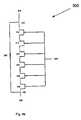
- FIG. 3illustrates an exemplary schematic diagram of a switch 200 , according to one embodiment of the present invention.
- the switch 200has a total of six gates 210 - 235 .
- the use of six gatesallows the switch 200 to operate at a low control voltage without the need to increase device periphery or die size.
- the FETs utilized in switch 200can have any number of gates as long as the total number of gates in the switch 200 equals six.
- the switch 200can utilize three dual gate FETs, two tri-gate FETS, or a mixed gate architecture where the FETs within the switch 200 have different number of gates (i.e., a first FET having three gates, a second FET having two gates, and a third FET having a single gate).
- FIG. 3clearly identifies the six gates 210 - 235 but does not identify the individual FETs that provide the six gates, as there are multiple different variations of FETs that can form the six gates.
- a first (uppermost or top) source 205is connected to a source voltage input 242 , each the gates 210 - 235 is coupled together and connected to a control voltage input 245 , and a last (lowermost or bottom) drain 240 is connected to an output 250 .
- a bypass resistance topology 260is coupled in parallel to the FETs (gates 210 - 235 ) from the source voltage input 242 (uppermost source 205 ) to the output 250 (lowermost drain 240 ). As previously mentioned, the bypass resistance topology 260 is not limited to being coupled in parallel with each FET.
- FIG. 4 aillustrates an exemplary schematic diagram of a switch 300 , according to one embodiment of the current invention.
- the switch 300includes a total of six gates 310 - 335 .
- any combination of FETscan be utilized to form the switch 300 having six gates.
- the inventionis not limited to six gates as other embodiments may have any number of gates.
- a first source 305is connected to a source voltage input 342
- each of the gates 310 - 335is coupled together and connected to a control voltage input 345
- a last drain 340is connected to an output 350 .
- the switch 300includes a resistor 360 (bypass resistance topology) coupled in parallel to all the FETs (gates 310 - 335 ) from the source voltage input 342 (first source 305 ) to the output 350 (last drain 340 ).
- the resistor 360is illustrated as a single resistor, however it is not limited thereto. Rather as one of ordinary skill in the art would recognize, the resistor 360 could include a plurality of resistors in series, could be any other type of resistive element, or could be a combination of same or different resistive types in series with one another without departing from the scope of the current invention.
- the resistor 360limits the output (current) of the switch prior to the control voltage reaching the pinch-off value (see previous discussion with relation to FIG. 2 ).
- the use of the resistor 360focuses the increase of precision activation timing on the whole switch 300 instead of the individual FETs making up the switch (linearity is not an issue).
- One preferred implementation of the exemplary embodiment of FIG. 4 ais for devices that do not require high linearity from switches utilized therein. Since the linearity of the switch, and each of the FETs that make up the switch, is not a critical issue, one bypass resistor can be used to sharpen the control voltage of the overall switch 300 .
- Another preferred implementation of this embodimentis for devices that require high power switches that will output a relatively large current once the switch is activated.
- the use of a relatively large resistor 360will limit (and ideally prevent) the switch from outputting a large current until the control voltage reaches the pinch-off value and each of the FETs and the switch 300 is activated.
- the exemplary switch 300can be used in devices where a high power output maybe desired, such as GSM devices.
- the use of the switch 300 in a particular device or for a particular applicationis based on more than just the type of bypass resistance topology that is used.
- the use of the switchalso depends on other factures, including but not limited to, the characteristics of the FETs, the number of FETs, and the source voltage supplied.
- the switch 300is not limited to high power devices and can be used in any now known or later discovered device where a solid-state switch is required, such as high frequency signal transmission systems, including but not limited to, Wireless LAN, Bluetooth, CDMA, TDMA, GSM and W-CDMA.
- FIG. 4 billustrates an exemplary schematic diagram of a switch 302 , according to one embodiment of the current invention.
- the switch 302is identical to the switch 300 of FIG. 4 a with the exception that switch 302 includes a plurality of resistors 362 - 372 (bypass resistance topology), with one resistor coupled across (in parallel to) each FET.
- the switch 302has six single-gate FETs with one resistor coupled across each single-gate FET of the switch 302 .
- the embodimentis not limited to the illustrated six single-gate FETs, and as previously discussed, other embodiments of the current invention may include switches having any number of FETs and any number of gates. Rather, this embodiment is illustrating that a resistor may be coupled in parallel to each single-gate FET of a switch.
- the resistors 362 - 372are illustrated as single resistors, however they are not limited thereto. Rather as one of ordinary skill in the art would recognize, the resistors 362 - 372 could include a plurality of resistors in series, could be any other type of resistive element, or could be a combination of same or different resistive types in series with one another without departing from the scope of the current invention.
- the use of the resistors 362 - 372 for each single-gate FETfocuses the increase of precision activation timing on each individual FET included in the switch (high linearity).
- each of the FETs of the switch 302has the same or substantially the same performance characteristics, so that they theoretically function in the same manner (identical characteristics, such as activation timing and leakage).
- each FETwill likely have slightly different characteristics due to different variables, including the processing of the chip. However, these differences of characteristics are normally relatively small or negligible and cannot be accounted for prior to processing.
- each resistor 362 - 372has the same resistance value so as to maintain linearity between each of the FETs.
- embodimentsare not limited to resistors 362 - 372 having the same value. In some embodiments it may be desirable or necessary to utilize different valued resistors. For example, if the characteristics of the FETs where not the same, for some reason, the bypass resistors could be selected so as to increase the linearity of the different FETs. Potential reasons for the FETs having different characteristics may include the location of the FET on the chip, the processing of the chip, the design of the switch, the distance from the source voltage or control voltage, other devices (i.e., feed-forward capacitors) connected to the FET, or inherent resistance in the board.
- a different value resistormay be used to reduce or eliminate the differences and maintain linearity.
- Another examplemay be that the path between a certain source and drain had a different resistance value due to, for example, length of path so that more or less resistance could be used to account for the difference.
- a switch designerwould recognize there are multiple scenarios that could cause a switch designer to use varying value resistors in the design of switches utilizing bypass resistors in the manner captured by the embodiment of FIG. 4 b.
- One preferred implementation of the exemplary embodiment of FIG. 4 bis for devices that require high linearity from switches utilized therein. Since the linearity of the switch, and each of the FETs that make up the switch, is important, individual resistors coupled across (in parallel to) each FET assist in decreasing (and ideally removing) the differences in performance (activation timing) of each of the individual FETs by increasing the precision timing of the activation of each FET (switch turn on) and thus the linearity of the switch 302 .
- Another preferred implementation of this embodimentis for devices that require low power switches that will output a relatively low current once the switch is activated.
- resistors 362 - 372can increase the precision timing of each FET and the switch 302 , so as to limit (and ideally prevent) the output of a low powered switch (low output current) until the control voltage reaches the pinch-off level and each of the FETs and the switch 302 is activated.
- the exemplary switch 302can be used for devices where r low power is desired, such as CDMA devices.
- the use of the switch 302 in a particular device or for a particular applicationis based on more than just the type of bypass resistance topology that is used.
- the use of the switchalso depends on other factures, including but not limited to, the characteristics of the FETs, the number of FETs, and the source voltage supplied.
- the switch 302is not limited to low power devices and can be used in any now known or later discovered device where a solid-state switch is required, such as high frequency signal transmission systems including Wireless LAN, Bluetooth, CDMA, TDMA, GSM and W-CDMA.
- FIG. 4 cillustrates an exemplary schematic diagram of a switch 304 , according to one embodiment of the current invention.
- the switch 304is identical to the switch 302 of FIG. 4 b with the exception that switch 304 includes a plurality of resistors 374 - 378 (bypass resistance topology), with one resistor coupled across (in parallel to) each FET.
- the switch 304has three dual-gate FETs with one resistor coupled across each dual-gate FET of the switch 304 .
- the inventionis not limited to the illustrated three dual-gate FETs, as previously discussed other embodiments of the current invention may include switches having any number of FETs and any number of gates. Rather, this embodiment is illustrating that a resistor may be coupled in parallel to each multi-gate FET of a switch.
- the resistors 374 - 378are illustrated as single resistors, however they are not limited thereto. Rather as one of ordinary skill in the art would recognize, the resistors 374 - 378 could include a plurality of resistors in series, could be any other type of resistive element, or could be a combination of same or different resistive types in series with one another without departing from the scope of the current invention. As mentioned above the resistors 374 - 378 may have the same values but are not limited thereto.
- the embodiment of FIG. 4 ccan be used in the same devices or for the same applications as those mentioned above with respect to FIG. 4 b . However, utilizing multi-gate FETs will allow this embodiment to have a smaller die size then the embodiment illustrated in FIG. 4 b.
- FIGS. 4 a - 4 cillustrated various exemplary embodiments of resistors used as a bypass path to sharpen the control voltage of the switch and increase the precise timing of the switch activation. All of the embodiments illustrated in these figures have a parallel path for either each FET or the entire series of FETs making up the switch. The invention is in no way intended to be limited thereto. Rather any combination of resistors can be used on any combination of FETs without departing from the scope of the current invention.
- a resistormay be used as a bypass path for any subset of successive FETs used in the switch (i.e., single resistor coupled in parallel to FETs having gates 315 - 330 ), or resistors may to used as a bypass path for any combination of FETs used in the switch (i.e., a first resistor in parallel to FETs having gates 315 and 320 , and a second resistor in parallel to FET having gate 335 ).
- FIG. 5illustrates an exemplary schematic diagram of a switch 400 , according to one embodiment of the present invention.
- the switch 400includes a total of six gates 410 - 435 .
- any combination of FETscan be utilized to form the switch 400 having six gates.
- the embodimentis not limited to six gates as other embodiments may have any number of gates.
- a first source 405is connected to a source voltage input 442 , each of the gates 410 - 435 is coupled together and connected to a control voltage input 445 , a last drain 440 is connected to an output 450 , and a bypass resistance topology 460 is coupled in parallel to all the FETs (gates 410 - 435 ) from the source voltage input 442 (first source 405 ) to the output 450 (last drain 440 ).
- the bypass resistance topology 460is not limited to being in parallel with all the FETs at once, nor is it limited to being in parallel with all of the FETs.
- the switch 400further includes a first feed-forward capacitor 470 coupled between the uppermost source 405 and the gate 410 and a second feed-forward capacitor 480 coupled between the lowermost drain 440 and the gate 435 .
- the feed-forward capacitors 470 , 480are used to reduce signal distortion and improve the linearity and harmonic noise rejection characteristics of a FET.
- the feed-forward capacitors 470 , 480may include a capacitor bottom metal layer, a dielectric layer formed on the bottom layer, and a capacitor top metal layer formed on the dielectric layer.
- at least a portion of the top metal layer of the first feed forward capacitor 470acts as the uppermost source 405
- at least a portion of the top metal layer of the second feed forward capacitor 480acts as the lowermost drain 440 .
- At least a portion of the gate 410 and at least a portion of gate 435are connected to at least a portion of the capacitor bottom metal layer of the first capacitor 470 and the second capacitor 480 respectively.
- the source and drain of each FETinclude fingers and the gates are located between the source fingers and the drain fingers.
- the gatesare serpentine gates that wind between the source and drain fingers and are connected to the capacitor bottom metal layer (of the source or drain accordingly) at various points.
- the serpentine gatesare connected to the capacitor bottom metal layer symmetrically.
- the gates of the FETsare buss gates that are connected to the capacitor bottom metal layer and protrude between source and drain fingers respectively.
- the FETsmay have a plurality of serpentine gates, a plurality of buss gates, a plurality of other gate types, or a combination thereof.
- FIG. 5illustrates an exemplary use of two feed-forward capacitors, one between the uppermost source and gate and one between the lowermost drain and gate, however, the invention is in no way intended to be limited thereto. Rather, other embodiments of the current invention could include more or less feed-forward capacitors, and the capacitors could be coupled to different FETs without departing from the scope of the current invention. For example, one embodiment could include in addition to the two feed forward capacitors of switch 400 a third feed-forward capacitor coupled between gate 425 and the associated source (or drain). Another embodiment, could include two feed-forward capacitors, one coupled between gate 415 and the associated source and one coupled between gate 430 and the associated drain.
- FIG. 6 aillustrates an exemplary schematic diagram of switch 500 , according to one embodiment of the present invention.
- the switch 500includes a total of six gates 510 - 535 (as previously discussed the invention is not limited to six gates and any combination of FETs can be utilized to form a switch having any total number of gates).
- a first source 505is connected to a source voltage input 542
- a last drain 540is connected to an output 550
- a bypass resistance topology 560is coupled in parallel to all the FETs.
- the switch 500also includes a gate resistance topology 570 coupled between each gate 510 - 535 and a control voltage input 545 .
- the gate resistance topology 570is used to minimize the effects of leakage current and reduce the resistor voltage drop for process points where FET diode leakage is an issue. As illustrated, the gate resistance topology 570 is connected between each gate and the control voltage input 545 , however, the current invention is not limited thereto. The gate resistance topology 570 could be coupled between only specific gates and the control voltage input 545 without departing from the scope of the current invention.
- FIG. 6 billustrates an exemplary schematic diagram of switch 501 , according to one embodiment of the present invention.
- the switch 501is identical to switch 500 , with the exception that resistors (first resistors) 572 - 582 act as the gate resistance topology 570 and are connected between each gate 510 - 535 and the control voltage input 545 .
- resistors 572 - 582act as the gate resistance topology 570 and are connected between each gate 510 - 535 and the control voltage input 545 .
- Each of the resistors 572 - 582is in parallel with each other.
- the resistors 572 - 582are illustrated as single resistors, however they are not limited thereto.
- the resistors 572 - 582could include a plurality of resistors in series, could be any other type of resistive element, or could be a combination of same or different resistive types in series with one another without departing from the scope of the current invention.
- each of the first resistors 572 - 582has the same value and thus reduces the leakage current for each FET the same.
- each FETdoes not necessarily have the same characteristics and each path from a FET to the control voltage input may not be the same, it is possible that the value of the resistors 572 - 582 will vary.
- One of ordinary skill in the art of switch designwould know how to design the switch to take in account differences that may require different valued resistors 572 - 582 .
- FIG. 6 cillustrates an exemplary schematic diagram of switch 502 , according to one embodiment of the present invention.
- the switch 502is identical to the switch 501 , with the exception that a second resistor 584 is included in series with each of the first resistors 572 - 582 .
- a second resistor 584is included in series with each of the first resistors 572 - 582 .
- each resistorcould include a plurality of resistors in series, could be any other type of resistive element, or could be a combination of same or different resistive types in series with one another without departing from the scope of the current invention.
- the addition of the second resistor 584increases the overall resistance between control voltage input 545 and each of the gates 510 - 535 and thus reduces the control current applied to the gate.
- This type of embodimentmay be used when it is not practical or beneficial to increase the value of each of the first resistors 572 - 582 .
- the addition of the extra resistoradds an additional voltage drop point and thus an additional leakage process point.
- the addition of the additional leakage process pointreduces the process stability of the switch as leakage through the resistor 584 could flow through each FET as that point is connected to all gates. As one of ordinary skill in the art would recognize, there is a tradeoff between lower leakage current and process stability.
- FIG. 6 dillustrates an exemplary schematic diagram of switch 503 , according to one embodiment of the present invention.
- the switch 503is identical to the switch 501 , with the exception that a plurality of second resistors 586 - 590 are included, each second resistor in series with a successive pair of first resistors 572 - 582 (i.e., second resistor 586 in series with first resistors 572 , 574 ).
- Each of the second resistors 586 - 590is in parallel with each other.
- each first resistor/second resistor pathi.e., 572 / 586 ) is in parallel with each other.
- resistors of switch 503are illustrated as single resistors, they are not limited thereto. As with the embodiment of FIG. 6 c , this type of embodiment may be used when it is not practical or beneficial to increase the value of each of the first resistors 572 - 582 .
- the addition of the extra resistors 586 - 590adds additional voltage drop points and thus an additional leakage process points. However, each additional leakage process point is only connected to two FETs so that any leakage through one of the second resistors 586 - 590 would only be promulgated to two FETs. Thus, this embodiment is more process stable than the embodiment illustrated in FIG. 6 c . As one of ordinary skill in the art would recognize, there is a tradeoff between lower leakage current and process stability.
- first resistors 572 - 582the second resistors 586 - 590 could all have the same resistance values, but are not limited thereto.
- each series combination of first and second resistorsi.e., first resistor 572 , second resistor 586 series resistance path
- first resistor 572the second resistor 586 series resistance path
- second resistor 586 series resistance pathmay have the same resistance value but are not limited thereto.
- One of ordinary skill in the art of switch designwould recognize how to select the values of the resistors.
- FIG. 6 eillustrates an exemplary schematic diagram of switch 504 , according to one embodiment of the present invention.
- the switch 504includes the same gates 510 - 535 , bypass resistance topology 560 , and source voltage input 542 and output 550 connections as all of the previously discussed embodiments of switches 500 - 503 .
- the switch 504also includes first resistors 572 , 582 , a plurality of second resistors 591 - 594 , and a third resistor 595 in series with each of the second resistors 591 - 594 .
- Each of the second resistors 591 - 594is in parallel with each other, and the first resistors 572 , 582 are in parallel with each of the second/third resistor paths (i.e., 591 / 595 ).
- the resistors of switch 504are illustrated as single resistors, they are not limited thereto.
- the second resistors 591 - 594could all have the same resistance values, but are not limited thereto.
- One of ordinary skill in the art of switch designwould recognize how to select the values of the resistors.
- the addition of the third resistor 595 to the second resistors 591 - 594increase the resistance and thus reduces the leakage current for each of the gates 515 - 530 . Utilizing resistors in series to increase the resistance is preferable when it is not practical or beneficial to increase the value of a single resistor.
- the addition of the third resistor 595adds an additional voltage drop point and thus an additional leakage process point.
- the addition of the additional leakage process pointreduces the process stability of the switch as leakage through the resistor 595 could flow through each FET connected thereto 510 - 530 . As one of ordinary skill in the art would recognize, there is a tradeoff between lower leakage current and process stability.
- the first resistors 572 , 582 and the second resistors 591 - 594have the same, or substantially the same, resistance values and the third resistor 595 increases the resistance and reduces the leakage current to the gates connected thereto (gates 510 - 530 ).
- the third resistor 595increases the resistance and reduces the leakage current to the gates connected thereto (gates 510 - 530 ).
- the combination of second and third resistors(i.e., 591 / 595 ) have the same, or substantially the same, resistance values as the first resistors 572 , 582 .
- the reduction in leakageshould be the same, or substantially the same, for each FET.
- the middle FETsobtain their leakage reduction with the use of resistors in series, while the uppermost and lowermost FETs utilize a single resistor to obtain the leakage reduction.
- FIG. 6 fillustrates an exemplary schematic diagram of switch 506 , according to one embodiment of the present invention.
- the switch 506is identical to the switch 504 with the exception that the third resistor 595 is replaced with two third resistors 596 , 597 .
- Each third resistor 596 , 597is coupled in series with each of two successive second resistors 591 / 592 , 593 / 594 respectively.
- the resistors of switch 506are illustrated as single resistors but are not limited thereto.
- the third resistors 596 , 597may have the same resistance value but are not limited thereto.
- Each third resistor 596 , 597adds an additional voltage drop point and potential leakage process point.
- each additional leakage process pointis only connected to two FETs so that any leakage through one of the third resistors 596 , 597 would only be promulgated to two FETs.
- this embodimentis more stable than the embodiment illustrated in FIG. 6 e .
- FIGS. 6 b - 6 frepresent examples of embodiments of the gate resistance topology that could be utilized in the low control voltage switch of the current invention, and in no way should be construed to limit the invention thereby. Rather, as one of ordinary skill in the art would recognize there are numerous gate resistor topologies that would be well within the scope of the current invention.
- FIGS. 5 and 6 a-fillustrate the independent addition of feed-forward capacitors ( 470 , 480 in FIG. 5) and gate resistance topology (i.e., 570 in FIG. 6 a ) respectively to six gate switches having a bypass resistance topology.
- feed-forward capacitors (any embodiment thereof) and gate resistance topology (any embodiment thereof)may be added to a switch in combination with one another.
- the feed-forward capacitors and/or the gate resistance topologymay be added to a switch having any embodiment of the bypass resistance topology (i.e., embodiments illustrated in FIGS. 4 a-c ).
- the feed-forward capacitors and/or the gate resistance topologymay be added to a switch having any number of FETs and any number of gates.
- the feed-forward capacitors and/or the gate resistance topologymay be added to a switch having any number of FETs and any number of gates.
- FET switchesare often utilized in communication devices, and are the preferred type of switch for high frequency signal transmission systems, such as Wireless LAN, Bluetooth, CDMA, TDMA, GSM and W-CDMA. Most high frequency signal transmission devices are continuing to get smaller while at the same time adding additional functions. Utilizing various embodiments of the current invention at the same time can produce an enhanced switch that does not require additional device periphery or die size (and preferably would reduce the die size). For example, utilizing a bypass resistance topology, feed-forward capacitors, a gate resistance topology and six-gates as discussed with respect to various embodiments of the current invention would produce a switch that had a low control voltage, sharpened control voltage (more precise activation timing) and less harmonics on the output.
- the function of the switchdictates the precise design of the switch.
- the precise design of the chipincludes, amongst other things, number, type and size of FETs, location of FETs and other periphery, bypass resistance topology, and gate resistance topology.
- linearityrefers to maximum power handling without distortion.
- linearityrefers to minimizing distortion of two low power signals traveling simultaneously in the same arm of a switch without generating any intermodulation distortion.
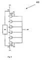
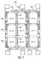
- FIG. 7illustrates an exemplary schematic diagram of a device 600 , such as a GSM device, which requires maximum power handling without distortion.
- the device 600includes a plurality of switches 610 (1 ⁇ n) .
- Each of the switches 610is in parallel with each other and is connected to same source voltage 620 .
- Each switch 610includes FETs having a total of six gates (single, multi or mixed gate FETs), a first feed-forward capacitor 630 connected to a first gate and an uppermost source, a second feed-forward capacitor 640 connected to a sixth gate and a lowermost drain, a single bypass resistor 650 , and a single gate resistor (gate resistance topology) coupled between each gate and a control voltage 660 .
- Each switch 610is provided with its own control voltage 660 (or connects to the same control voltage via a separate controllable path) and produces its own output 670 .
- the utilization of a single bypass resister 650indicates that the switches are high power switches, as single bypass resistors are utilized to sharpen the control voltage and increase the activation efficiency of high-powered switches (see previous disclosure related to FIG. 4 a ).
- switchesthat could be used in devices requiring high power switches that would be well within the scope of the current invention.
- different gate resistor topologiescould be used.
- the devicesare not limited to the illustrated configuration where all of the switches are in parallel and are connected to the same control source.
- the plurality of switchescould be connected to the same control voltage source, or the plurality of switches could be connected to separate source voltage sources.
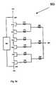
- FIG. 8illustrates an exemplary schematic diagram of a device 700 , such as CDMA device, requiring low power.
- the device 700includes a plurality of switches 710 (1 ⁇ n) .
- Each of the switches 710is in parallel with each other and is connected to same source voltage 720 .
- Each switch 710includes a plurality of FETs (illustrated as single gate FETs), a first feed-forward capacitor 730 connected to a first gate and an uppermost source, a second feed-forward capacitor 740 connected to a sixth gate and a lowermost drain, a bypass resistor coupled across each FET, and a single resistor (gate resistance topology) coupled between each gate and a control voltage 750 .
- FETsillustrated as single gate FETs
- Each switch 710is provided with its own control voltage 750 and produces its own output 760 .
- the utilization of a single bypass resister for each FETprovides that the switches are high linearity switches, as single bypass resistors are utilized to sharpen the control voltage and increase the activation efficiency of each individual FET within the switch (see previous disclosure related to FIG. 4 b and 3 c ).
- switchesthat could be used in devices requiring high linearity switches that would be well within the scope of the current invention.
- different gate resistor topologiescould be used or multi-gate FETs could be used.
- the devicesare not limited to the illustrated configuration where all of the switches are in parallel and are connected to the same control source.
- the plurality of switchescould be connected to the same control voltage source, or the plurality of switches could be connected to separate source voltage sources.
- FIG. 7illustrates a device requiring high power switches
- FIG. 8illustrates a device requiring high linearity switches.
- the devices 600 , 700used a plurality of identical switches 610 (1 ⁇ n) , 710 (1 ⁇ n) .
- the inventionshould not be construed to be limited thereby.
- the devices 600 , 700could utilize a variety of different type of switches as long as the switch fit the purpose of the device.
- a device requiring three high power switchescould utilize a first high-power switch having single gate FETS and a single resistor in parallel from a gate of each FET to a control voltage source (i.e., as illustrated in the exemplary switch 501 of FIG.
- a second high-power switchutilizing dual gate FETs and a single resistor in parallel from the gate of each FET to the control voltage source (i.e., switch 501 ), and a third high-power switch having dual gate FETs and a plurality of resisters in parallel from the gate of each FET to the control voltage source (i.e., as illustrated in exemplary switches 502 , 503 of FIGS. 6 c - 6 d ).
- the inventionis not limited to devices (such as devices 600 , 700 ) that require only one type of switch (i.e., high power, low power). Rather, as one skilled in the art would recognize a device could have multiple different types of switches without departing from the scope of the current invention. For example, a device may have both high power and lower switches contained therein.
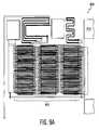
- FIG. 9-9Dillustrate an exemplary chip layout of a device 800 utilizing switches, according to one embodiment of the current invention.
- the device 800has four parallel sections 802 , 804 , 806 , 808 .
- Each sectionutilizes 3 dual gate FETs to produce a six-gate switch.
- the source voltage 810connects to a source of a first FET of each switch.
- the specific chip layout of the third switch 806will now be described, with each other switch 802 , 804 , 808 having an identical layout.
- the source of a first FET 820is the top capacitor metal layer of a first feed-forward capacitor (or at least a portion of the top capacitor metal layer) as described previously. Dual gates wind between the source and the drain of the first FET 820 .
- the gates (or at least a portion of the gates) of the first FETare connected to the lower capacitor metal layer (or at least a portion of the lower capacitor metal layer) of the first feed-forward capacitor.
- the drain of the first FET 820is connected to a source of a second FET 830 . Dual gates wind between the source and the drain of the second FET 830 .
- the drain of the second FET 830is connected to a source of a third FET 840 .
- the drain of the third FET 840is the top capacitor metal layer of a second feed-forward capacitor (or at least a portion of the top capacitor metal layer).
- the gates (or at least a portion of the gates) of the third FET 840are connected to the lower capacitor metal layer (or at least a portion of the lower capacitor metal layer) of the second feed-forward capacitor.
- the drain of the third FET 840is connected to the output 850 .
- Each of the gates of each FET 820 , 830 , 840is connected to a control voltage 860 via a single resistive path 870 .
- the combination of each single resistive path 870makes up the gate resistance topology (corresponding to exemplary schematic of switch 501 illustrated in FIG. 6 b ).
- a single resistive path 880connects the source of the first FET 820 to the drain of the last FET 840 .
- the single resistive path 880is the bypass resistance topology (corresponding to exemplary schematic of switch 300 illustrated in FIG. 4 a ), which results in a high power switch. As previously discussed, this type of switch is likely utilized in (but is not limited to) high power communication devices, such as GSM devices.
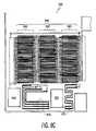
- FIG. 10-10Billustrate an exemplary chip layout of a device 900 utilizing switches, according to one embodiment of the current invention.
- the device 900has two parallel sections 910 , 920 . Each section utilizes three FETs 930 , 940 , 950 having a mixed gate architecture.
- the first FET 930has two gates and two resistive paths 960 connected from the gates of the first FET 930 to a control voltage 970 .
- the second FET 940has three gates and three resistive paths 960 connected from the gates of the second FET 940 to the control voltage 970 .
- the third FET 950has one gate and one resistive path 960 connected from the gate of the third FET 950 to the control voltage 970 .
- bypass resistor 980that connects the source of the first FET 930 and the drain of the third FET 950 (corresponding to exemplary schematic of switch 300 illustrated in FIG. 4 a ), which indicates the switch as being a high power switch.
- this type of switchis likely utilized in (but is not limited to) high power communication devices, such as GSM devices
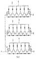
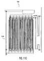
- FIG. 11-11Iillustrate an exemplary chip layout of a device 1000 utilizing switches, according to one embodiment of the current invention.
- the device 1000has three parallel sections 1010 , 1020 , 1030 . Each section utilizes three dual-gate FETs 1040 , 1050 , 1060 .
- a bypass resistor 1070 , 1080 , 1090is coupled across each dual gate FET 1040 , 1050 , 1060 respectively.
- the three bypass resistors 1070 - 1090make up the bypass resistance topology (corresponding to exemplary schematic of switch 304 illustrated in FIG. 4 c ) and indicates that the switch is a high linearity switch. As previously discussed, this type of switch is likely utilized in (but is not limited to) communication devices, such as CDMA devices, where low power can be utilized.
Landscapes
- Electronic Switches (AREA)
Abstract
Description
Claims (52)
Priority Applications (1)
| Application Number | Priority Date | Filing Date | Title |
|---|---|---|---|
| US10/390,957US6803680B2 (en) | 2002-09-13 | 2003-03-18 | Apparatus, methods, and articles of manufacture for a switch having sharpened control voltage |
Applications Claiming Priority (2)
| Application Number | Priority Date | Filing Date | Title |
|---|---|---|---|
| US41064702P | 2002-09-13 | 2002-09-13 | |
| US10/390,957US6803680B2 (en) | 2002-09-13 | 2003-03-18 | Apparatus, methods, and articles of manufacture for a switch having sharpened control voltage |
Publications (2)
| Publication Number | Publication Date |
|---|---|
| US20040051395A1 US20040051395A1 (en) | 2004-03-18 |
| US6803680B2true US6803680B2 (en) | 2004-10-12 |
Family
ID=31997353
Family Applications (1)
| Application Number | Title | Priority Date | Filing Date |
|---|---|---|---|
| US10/390,957Expired - LifetimeUS6803680B2 (en) | 2002-09-13 | 2003-03-18 | Apparatus, methods, and articles of manufacture for a switch having sharpened control voltage |
Country Status (1)
| Country | Link |
|---|---|
| US (1) | US6803680B2 (en) |
Cited By (54)
| Publication number | Priority date | Publication date | Assignee | Title |
|---|---|---|---|---|
| US20030116780A1 (en)* | 2001-12-20 | 2003-06-26 | Atsushi Suwa | Field effect transistor switch circuit |
| US20040195585A1 (en)* | 2002-12-05 | 2004-10-07 | University Of Massachusetts Lowell | Multi-gate heterostructured field effect transistor |
| US20040207454A1 (en)* | 2003-04-16 | 2004-10-21 | Matsushita Electric Industrial Co., Ltd. | High Frequency switch circuit |
| US20040251952A1 (en)* | 2003-06-12 | 2004-12-16 | Matsushita Electric Industrial Co., Ltd. | High-frequency switching device and semiconductor |
| US20050007179A1 (en)* | 2003-07-07 | 2005-01-13 | Murata Manufacturing Co., Ltd. | High-frequency switching circuit |
| US20050017786A1 (en)* | 2003-06-13 | 2005-01-27 | Matsushita Electric Industrial Co., Ltd. | Hight frequency switching circuit and semiconductor device |
| US20060160520A1 (en)* | 2004-01-16 | 2006-07-20 | Naoyuki Miyazawa | Radio frequency switch |
| US20060214238A1 (en)* | 2005-03-28 | 2006-09-28 | Glass Elizabeth C | Multi-gate enhancement mode RF switch and bias arrangement |
| US20060217078A1 (en)* | 2005-03-28 | 2006-09-28 | Glass Elizabeth C | Enhancement mode transceiver and switched gain amplifier integrated circuit |
| US20070058306A1 (en)* | 2005-09-15 | 2007-03-15 | Rambus, Inc. | Power supply shunt |
| US20070243849A1 (en)* | 2006-04-17 | 2007-10-18 | Skyworks Solutions, Inc. | High-frequency switching device with reduced harmonics |
| US20080012782A1 (en)* | 2006-06-28 | 2008-01-17 | Filtronic Compound Semiconductors Limited | Linear antenna switch arm and a field effect transistor |
| US20080079514A1 (en)* | 2006-10-02 | 2008-04-03 | Skyworks Solutions, Inc. | Harmonic phase tuning filter for RF switches |
| US7459988B1 (en) | 2006-09-18 | 2008-12-02 | Rf Micro Devices, Inc. | High linearity wide dynamic range radio frequency antenna switch |
| US7646260B2 (en) | 2007-07-13 | 2010-01-12 | Skyworks Solutions, Inc. | Switching device with selectable phase shifting modes for reduced intermodulation distortion |
| US7817966B2 (en) | 2007-07-13 | 2010-10-19 | Skyworks Solutions, Inc. | Switching device with reduced intermodulation distortion |
| US7982243B1 (en) | 2006-05-05 | 2011-07-19 | Rf Micro Devices, Inc. | Multiple gate transistor architecture providing an accessible inner source-drain node |
| US20110260774A1 (en)* | 2010-04-27 | 2011-10-27 | Rf Micro Devices, Inc. | High power fet switch |
| CN102474249A (en)* | 2009-07-28 | 2012-05-23 | 高通股份有限公司 | Switch with improved biasing |
| US20130015903A1 (en)* | 2011-07-13 | 2013-01-17 | Yu Sin Kim | Resistor-sharing switching circuit |
| US8405147B2 (en) | 2005-07-11 | 2013-03-26 | Peregrine Semiconductor Corporation | Method and apparatus for use in improving linearity of MOSFETs using an accumulated charge sink |
| US20130215540A1 (en)* | 2012-02-16 | 2013-08-22 | Newport Media, Inc. | High Voltage Electrostatic Discharge Clamp Using Deep Submicron CMOS Technology |
| US8536636B2 (en) | 2007-04-26 | 2013-09-17 | Peregrine Semiconductor Corporation | Tuning capacitance to enhance FET stack voltage withstand |
| US20130249619A1 (en)* | 2009-09-11 | 2013-09-26 | Rf Micro Devices, Inc. | Soi switch enhancement |
| US8559907B2 (en) | 2004-06-23 | 2013-10-15 | Peregrine Semiconductor Corporation | Integrated RF front end with stacked transistor switch |
| US8583111B2 (en) | 2001-10-10 | 2013-11-12 | Peregrine Semiconductor Corporation | Switch circuit and method of switching radio frequency signals |
| US8604864B2 (en) | 2008-02-28 | 2013-12-10 | Peregrine Semiconductor Corporation | Devices and methods for improving voltage handling and/or bi-directionality of stacks of elements when connected between terminals |
| US8723260B1 (en) | 2009-03-12 | 2014-05-13 | Rf Micro Devices, Inc. | Semiconductor radio frequency switch with body contact |
| US8742502B2 (en) | 2005-07-11 | 2014-06-03 | Peregrine Semiconductor Corporation | Method and apparatus for use in improving linearity of MOSFETs using an accumulated charge sink-harmonic wrinkle reduction |
| US20140240030A1 (en)* | 2013-02-26 | 2014-08-28 | Kabushiki Kaisha Toshiba | Semiconductor Switch Circuit |
| US8954902B2 (en) | 2005-07-11 | 2015-02-10 | Peregrine Semiconductor Corporation | Method and apparatus improving gate oxide reliability by controlling accumulated charge |
| US8994448B2 (en)* | 2013-03-29 | 2015-03-31 | Peregrine Semiconductor Corporation | Systems and methods for generation of internal chip supply bias from high voltage control line inputs |
| US20150171860A1 (en)* | 2013-11-13 | 2015-06-18 | Skyworks Solutions, Inc. | Circuits and methods for improved quality factor in a stack of transistors |
| US9172404B1 (en) | 2005-02-07 | 2015-10-27 | Rf Micro Devices, Inc. | Switch architecture for TDMA and FDD multiplexing |
| US20150311883A1 (en)* | 2014-04-29 | 2015-10-29 | Infineon Technologies Ag | System and Method for a Switchable Capacitance |
| US9209784B2 (en) | 2010-04-27 | 2015-12-08 | Rf Micro Devices, Inc. | Switchable capacitive elements for programmable capacitor arrays |
| US9397656B2 (en) | 2005-07-11 | 2016-07-19 | Peregrine Semiconductor Corporation | Circuit and method for controlling charge injection in radio frequency switches |
| US9406695B2 (en) | 2013-11-20 | 2016-08-02 | Peregrine Semiconductor Corporation | Circuit and method for improving ESD tolerance and switching speed |
| US9419565B2 (en) | 2013-03-14 | 2016-08-16 | Peregrine Semiconductor Corporation | Hot carrier injection compensation |
| US9590674B2 (en) | 2012-12-14 | 2017-03-07 | Peregrine Semiconductor Corporation | Semiconductor devices with switchable ground-body connection |
| US9742400B2 (en)* | 2015-05-06 | 2017-08-22 | Infineon Technologies Ag | System and method for driving radio frequency switch |
| US9831857B2 (en) | 2015-03-11 | 2017-11-28 | Peregrine Semiconductor Corporation | Power splitter with programmable output phase shift |
| US9948281B2 (en) | 2016-09-02 | 2018-04-17 | Peregrine Semiconductor Corporation | Positive logic digitally tunable capacitor |
| US10148265B2 (en)* | 2015-01-30 | 2018-12-04 | Psemi Corporation | Radio frequency switching circuit with distributed switches |
| US10211830B2 (en) | 2017-04-28 | 2019-02-19 | Qualcomm Incorporated | Shunt termination path |
| US10236872B1 (en) | 2018-03-28 | 2019-03-19 | Psemi Corporation | AC coupling modules for bias ladders |
| US10320379B2 (en) | 2016-12-21 | 2019-06-11 | Qorvo Us, Inc. | Transistor-based radio frequency (RF) switch |
| US10505530B2 (en) | 2018-03-28 | 2019-12-10 | Psemi Corporation | Positive logic switch with selectable DC blocking circuit |
| US10608623B2 (en) | 2016-12-21 | 2020-03-31 | Qorvo US. Inc. | Transistor-based radio frequency (RF) switch |
| US10886911B2 (en) | 2018-03-28 | 2021-01-05 | Psemi Corporation | Stacked FET switch bias ladders |
| US11011633B2 (en) | 2005-07-11 | 2021-05-18 | Psemi Corporation | Method and apparatus for use in improving linearity of MOSFETs using an accumulated charge sink-harmonic wrinkle reduction |
| USRE48965E1 (en) | 2005-07-11 | 2022-03-08 | Psemi Corporation | Method and apparatus improving gate oxide reliability by controlling accumulated charge |
| US11476849B2 (en) | 2020-01-06 | 2022-10-18 | Psemi Corporation | High power positive logic switch |
| US20250167542A1 (en)* | 2023-11-16 | 2025-05-22 | Richwave Technology Corp. | Transistor stack circuit |
Families Citing this family (9)
| Publication number | Priority date | Publication date | Assignee | Title |
|---|---|---|---|---|
| US20060086974A1 (en)* | 2004-10-26 | 2006-04-27 | Power Integrations, Inc. | Integrated circuit with multi-length power transistor segments |
| US7872502B2 (en)* | 2006-07-12 | 2011-01-18 | Hewlett-Packard Development Company, L.P. | Defect-and-failure-tolerant demultiplexer using series replication and error-control encoding |
| WO2008133620A1 (en)* | 2007-04-26 | 2008-11-06 | University Of Florida | High power t/r switch using stacked transistors |
| US8796772B2 (en)* | 2012-09-24 | 2014-08-05 | Intel Corporation | Precision resistor for non-planar semiconductor device architecture |
| JP6338832B2 (en) | 2013-07-31 | 2018-06-06 | ルネサスエレクトロニクス株式会社 | Semiconductor device |
| US9143124B2 (en)* | 2014-02-18 | 2015-09-22 | Acco | Switch controls |
| CN105515561A (en)* | 2015-12-01 | 2016-04-20 | 唯捷创芯(天津)电子技术股份有限公司 | Multipath switching circuit, chip and communication terminal |
| CN106972845A (en)* | 2017-04-07 | 2017-07-21 | 广东工业大学 | A kind of radio-frequency switch circuit |
| CN116054802A (en)* | 2023-01-09 | 2023-05-02 | 深圳飞骧科技股份有限公司 | A radio frequency switch circuit |
Citations (43)
| Publication number | Priority date | Publication date | Assignee | Title |
|---|---|---|---|---|
| JPS5914647A (en)* | 1982-07-16 | 1984-01-25 | Nec Corp | Master-slice semiconductor device |
| US4435652A (en) | 1981-05-26 | 1984-03-06 | Honeywell, Inc. | Threshold voltage control network for integrated circuit field-effect trransistors |
| US4631470A (en)* | 1985-12-13 | 1986-12-23 | Rca Corporation | Current surge limited power supply |
| US4837530A (en)* | 1987-12-11 | 1989-06-06 | Hewlett-Packard Company | Wideband (DC-50 GHz) MMIC FET variable matched attenuator |
| US4849903A (en)* | 1987-07-15 | 1989-07-18 | The United States Of America As Represented By The Administrator Of The National Aeronautics And Space Administration | Digitally controlled system for effecting and presenting a selected electrical resistance |
| US4877976A (en) | 1987-03-13 | 1989-10-31 | Gould Inc. | Cascade FET logic circuits |
| US4890077A (en)* | 1989-03-28 | 1989-12-26 | Teledyne Mec | FET monolithic microwave integrated circuit variable attenuator |
| US5012123A (en)* | 1989-03-29 | 1991-04-30 | Hittite Microwave, Inc. | High-power rf switching system |
| JPH046958A (en)* | 1990-04-24 | 1992-01-10 | Toshiba Corp | Horizontal deflection circuit |
| US5216587A (en)* | 1991-04-05 | 1993-06-01 | Hitachi, Ltd. | Inverter |
| US5333104A (en)* | 1992-05-22 | 1994-07-26 | Matsushita Electric Works, Ltd. | Inverter power source |
| US5384501A (en)* | 1990-06-15 | 1995-01-24 | Kabushiki Kaisha Toshiba | Integration circuit including a differential amplifier having a variable transconductance |
| US5469195A (en) | 1991-01-24 | 1995-11-21 | Texas Instruments Incorporated | Integrated circuit capacitors, buffers, systems and methods |
| US5488552A (en)* | 1992-10-07 | 1996-01-30 | Hiroshi Sakamoto | Inverter power supply |
| US5592353A (en)* | 1994-04-18 | 1997-01-07 | Fujitsu Limited | Power supply system |
| US5594441A (en) | 1994-12-30 | 1997-01-14 | Psc, Inc. | D/A converter with constant gate voltage |
| US5600602A (en) | 1995-04-05 | 1997-02-04 | Micron Technology, Inc. | Hierarchical memory array structure having electrically isolated bit lines for temporary data storage |
| US5614771A (en)* | 1995-12-27 | 1997-03-25 | Xerox Corporation | Extended high voltage SCR switch |
| US5656956A (en)* | 1995-03-28 | 1997-08-12 | Mitsubishi Denki Kabushiki Kaisha | Logic gate circuit and digital integrated circuit |
| US5675290A (en)* | 1995-08-09 | 1997-10-07 | Mitsubishi Denki Kabushiki Kaisha | Microwave amplifier circuit |
| US5748053A (en) | 1995-09-28 | 1998-05-05 | Kabushiki Kaisha Toshiba | Switching circuit |
| US5852360A (en)* | 1997-04-18 | 1998-12-22 | Exar Corporation | Programmable low drift reference voltage generator |
| US5903177A (en)* | 1996-09-05 | 1999-05-11 | The Whitaker Corporation | Compensation network for pinch off voltage sensitive circuits |
| US5969560A (en)* | 1995-01-23 | 1999-10-19 | Sony Corporation | Switching circuit at high frequency with low insertion loss |
| US5973552A (en)* | 1996-11-04 | 1999-10-26 | Mosaid Technologies Incorporated | Power savings technique in solid state integrated circuits |
| US5970964A (en)* | 1995-12-18 | 1999-10-26 | Fuji Electric Co., Ltd. | Circuit device for igniting internal combustion engine and semiconductor device for igniting internal combustion engine |
| US6094021A (en)* | 1998-11-12 | 2000-07-25 | Honda Giken Kogyo Kabushiki Kaisha | Motor drive apparatus |
| JP2001076897A (en)* | 1999-09-02 | 2001-03-23 | Yokogawa Electric Corp | Microwave oscillator |
| US6211726B1 (en) | 1999-06-28 | 2001-04-03 | International Business Machines Corporation | Low voltage, high-current electronic load |
| US6218890B1 (en)* | 1998-07-14 | 2001-04-17 | Sanyo Electric Co., Ltd. | Switching circuit device and semiconductor device |
| US6246598B1 (en)* | 2000-08-02 | 2001-06-12 | Polarity, Inc. | High-voltage modulator system |
| US6265925B1 (en)* | 1999-09-30 | 2001-07-24 | Intel Corporation | Multi-stage techniques for accurate shutoff of circuit |
| US6288458B1 (en) | 1999-09-30 | 2001-09-11 | Honeywell International Inc. | Power stealing solid state switch |
| US20010040479A1 (en) | 2000-03-03 | 2001-11-15 | Shuyun Zhang | Electronic switch |
| US6335577B1 (en)* | 1999-02-12 | 2002-01-01 | Yazaki Corporation | Power supply control unit and power supply control method |
| US6426525B1 (en) | 2001-04-18 | 2002-07-30 | Tyco Electronics Corporation | FET structures having symmetric and/or distributed feedforward capacitor connections |
| US6445729B1 (en)* | 1997-12-29 | 2002-09-03 | Samsung Electronics, Co., Ltd. | Radio signal transceiver apparatus |
| US6548363B1 (en)* | 2000-04-11 | 2003-04-15 | Taiwan Semiconductor Manufacturing Company | Method to reduce the gate induced drain leakage current in CMOS devices |
| US6563366B1 (en)* | 1997-10-30 | 2003-05-13 | Sony Corporation | High-frequency Circuit |
| US6577171B1 (en)* | 1999-11-25 | 2003-06-10 | Stmicroelectronics S.R.L. | Methods and apparatus for preventing inadvertent activation of power devices |
| US6664842B1 (en)* | 2001-12-28 | 2003-12-16 | Inphi Corporation | FET active load and current source |
| US6696680B2 (en)* | 2000-03-02 | 2004-02-24 | Sanyo Electric Co., Ltd. | Variable resistance circuit, operational amplification circuit and semiconductor integrated circuit |
| US6704550B1 (en)* | 1999-09-14 | 2004-03-09 | Sony Corporation | Antenna switching circuit and communication system using the same |
- 2003
- 2003-03-18USUS10/390,957patent/US6803680B2/ennot_activeExpired - Lifetime
Patent Citations (43)
| Publication number | Priority date | Publication date | Assignee | Title |
|---|---|---|---|---|
| US4435652A (en) | 1981-05-26 | 1984-03-06 | Honeywell, Inc. | Threshold voltage control network for integrated circuit field-effect trransistors |
| JPS5914647A (en)* | 1982-07-16 | 1984-01-25 | Nec Corp | Master-slice semiconductor device |
| US4631470A (en)* | 1985-12-13 | 1986-12-23 | Rca Corporation | Current surge limited power supply |
| US4877976A (en) | 1987-03-13 | 1989-10-31 | Gould Inc. | Cascade FET logic circuits |
| US4849903A (en)* | 1987-07-15 | 1989-07-18 | The United States Of America As Represented By The Administrator Of The National Aeronautics And Space Administration | Digitally controlled system for effecting and presenting a selected electrical resistance |
| US4837530A (en)* | 1987-12-11 | 1989-06-06 | Hewlett-Packard Company | Wideband (DC-50 GHz) MMIC FET variable matched attenuator |
| US4890077A (en)* | 1989-03-28 | 1989-12-26 | Teledyne Mec | FET monolithic microwave integrated circuit variable attenuator |
| US5012123A (en)* | 1989-03-29 | 1991-04-30 | Hittite Microwave, Inc. | High-power rf switching system |
| JPH046958A (en)* | 1990-04-24 | 1992-01-10 | Toshiba Corp | Horizontal deflection circuit |
| US5384501A (en)* | 1990-06-15 | 1995-01-24 | Kabushiki Kaisha Toshiba | Integration circuit including a differential amplifier having a variable transconductance |
| US5469195A (en) | 1991-01-24 | 1995-11-21 | Texas Instruments Incorporated | Integrated circuit capacitors, buffers, systems and methods |
| US5216587A (en)* | 1991-04-05 | 1993-06-01 | Hitachi, Ltd. | Inverter |
| US5333104A (en)* | 1992-05-22 | 1994-07-26 | Matsushita Electric Works, Ltd. | Inverter power source |
| US5488552A (en)* | 1992-10-07 | 1996-01-30 | Hiroshi Sakamoto | Inverter power supply |
| US5592353A (en)* | 1994-04-18 | 1997-01-07 | Fujitsu Limited | Power supply system |
| US5594441A (en) | 1994-12-30 | 1997-01-14 | Psc, Inc. | D/A converter with constant gate voltage |
| US5969560A (en)* | 1995-01-23 | 1999-10-19 | Sony Corporation | Switching circuit at high frequency with low insertion loss |
| US5656956A (en)* | 1995-03-28 | 1997-08-12 | Mitsubishi Denki Kabushiki Kaisha | Logic gate circuit and digital integrated circuit |
| US5600602A (en) | 1995-04-05 | 1997-02-04 | Micron Technology, Inc. | Hierarchical memory array structure having electrically isolated bit lines for temporary data storage |
| US5675290A (en)* | 1995-08-09 | 1997-10-07 | Mitsubishi Denki Kabushiki Kaisha | Microwave amplifier circuit |
| US5748053A (en) | 1995-09-28 | 1998-05-05 | Kabushiki Kaisha Toshiba | Switching circuit |
| US5970964A (en)* | 1995-12-18 | 1999-10-26 | Fuji Electric Co., Ltd. | Circuit device for igniting internal combustion engine and semiconductor device for igniting internal combustion engine |
| US5614771A (en)* | 1995-12-27 | 1997-03-25 | Xerox Corporation | Extended high voltage SCR switch |
| US5903177A (en)* | 1996-09-05 | 1999-05-11 | The Whitaker Corporation | Compensation network for pinch off voltage sensitive circuits |
| US5973552A (en)* | 1996-11-04 | 1999-10-26 | Mosaid Technologies Incorporated | Power savings technique in solid state integrated circuits |
| US5852360A (en)* | 1997-04-18 | 1998-12-22 | Exar Corporation | Programmable low drift reference voltage generator |
| US6563366B1 (en)* | 1997-10-30 | 2003-05-13 | Sony Corporation | High-frequency Circuit |
| US6445729B1 (en)* | 1997-12-29 | 2002-09-03 | Samsung Electronics, Co., Ltd. | Radio signal transceiver apparatus |
| US6218890B1 (en)* | 1998-07-14 | 2001-04-17 | Sanyo Electric Co., Ltd. | Switching circuit device and semiconductor device |
| US6094021A (en)* | 1998-11-12 | 2000-07-25 | Honda Giken Kogyo Kabushiki Kaisha | Motor drive apparatus |
| US6335577B1 (en)* | 1999-02-12 | 2002-01-01 | Yazaki Corporation | Power supply control unit and power supply control method |
| US6211726B1 (en) | 1999-06-28 | 2001-04-03 | International Business Machines Corporation | Low voltage, high-current electronic load |
| JP2001076897A (en)* | 1999-09-02 | 2001-03-23 | Yokogawa Electric Corp | Microwave oscillator |
| US6704550B1 (en)* | 1999-09-14 | 2004-03-09 | Sony Corporation | Antenna switching circuit and communication system using the same |
| US6265925B1 (en)* | 1999-09-30 | 2001-07-24 | Intel Corporation | Multi-stage techniques for accurate shutoff of circuit |
| US6288458B1 (en) | 1999-09-30 | 2001-09-11 | Honeywell International Inc. | Power stealing solid state switch |
| US6577171B1 (en)* | 1999-11-25 | 2003-06-10 | Stmicroelectronics S.R.L. | Methods and apparatus for preventing inadvertent activation of power devices |
| US6696680B2 (en)* | 2000-03-02 | 2004-02-24 | Sanyo Electric Co., Ltd. | Variable resistance circuit, operational amplification circuit and semiconductor integrated circuit |
| US20010040479A1 (en) | 2000-03-03 | 2001-11-15 | Shuyun Zhang | Electronic switch |
| US6548363B1 (en)* | 2000-04-11 | 2003-04-15 | Taiwan Semiconductor Manufacturing Company | Method to reduce the gate induced drain leakage current in CMOS devices |
| US6246598B1 (en)* | 2000-08-02 | 2001-06-12 | Polarity, Inc. | High-voltage modulator system |
| US6426525B1 (en) | 2001-04-18 | 2002-07-30 | Tyco Electronics Corporation | FET structures having symmetric and/or distributed feedforward capacitor connections |
| US6664842B1 (en)* | 2001-12-28 | 2003-12-16 | Inphi Corporation | FET active load and current source |
Cited By (115)
| Publication number | Priority date | Publication date | Assignee | Title |
|---|---|---|---|---|
| US8583111B2 (en) | 2001-10-10 | 2013-11-12 | Peregrine Semiconductor Corporation | Switch circuit and method of switching radio frequency signals |
| US10812068B2 (en) | 2001-10-10 | 2020-10-20 | Psemi Corporation | Switch circuit and method of switching radio frequency signals |
| US10797694B2 (en) | 2001-10-10 | 2020-10-06 | Psemi Corporation | Switch circuit and method of switching radio frequency signals |
| US9225378B2 (en) | 2001-10-10 | 2015-12-29 | Peregrine Semiconductor Corpopration | Switch circuit and method of switching radio frequency signals |
| US7138846B2 (en)* | 2001-12-20 | 2006-11-21 | Matsushita Electric Industrial Co., Ltd. | Field effect transistor switch circuit |
| US20030116780A1 (en)* | 2001-12-20 | 2003-06-26 | Atsushi Suwa | Field effect transistor switch circuit |
| US20040195585A1 (en)* | 2002-12-05 | 2004-10-07 | University Of Massachusetts Lowell | Multi-gate heterostructured field effect transistor |
| US20040207454A1 (en)* | 2003-04-16 | 2004-10-21 | Matsushita Electric Industrial Co., Ltd. | High Frequency switch circuit |
| US7106121B2 (en)* | 2003-04-16 | 2006-09-12 | Matsushita Electric Industrial Co., Ltd. | High frequency switch circuit |
| US20060181328A1 (en)* | 2003-06-12 | 2006-08-17 | Matsushita Electric Industrial Co., Ltd. | High-frequency switching device and semiconductor device |
| US20040251952A1 (en)* | 2003-06-12 | 2004-12-16 | Matsushita Electric Industrial Co., Ltd. | High-frequency switching device and semiconductor |
| US7199635B2 (en)* | 2003-06-12 | 2007-04-03 | Matsushita Electric Industrial Co., Ltd. | High-frequency switching device and semiconductor |
| US20070139094A1 (en)* | 2003-06-12 | 2007-06-21 | Matsushita Electric Industrial Co., Ltd. | High-frequency switching device and semiconductor |
| US7636004B2 (en)* | 2003-06-12 | 2009-12-22 | Panasonic Corporation | High-frequency switching device and semiconductor |
| US7286001B2 (en) | 2003-06-12 | 2007-10-23 | Matsushita Electric Industrial Co., Ltd. | High-frequency switching device and semiconductor device |
| US20050017786A1 (en)* | 2003-06-13 | 2005-01-27 | Matsushita Electric Industrial Co., Ltd. | Hight frequency switching circuit and semiconductor device |
| US7173471B2 (en)* | 2003-06-13 | 2007-02-06 | Matsushita Electric Industrial Co., Ltd. | High frequency switching circuit and semiconductor device |
| US7692472B2 (en)* | 2003-07-07 | 2010-04-06 | Murata Manufacturing Co., Ltd. | High-frequency switching circuit |
| US20050007179A1 (en)* | 2003-07-07 | 2005-01-13 | Murata Manufacturing Co., Ltd. | High-frequency switching circuit |
| US7561853B2 (en)* | 2004-01-16 | 2009-07-14 | Eudyna Devices Inc. | Radio frequency switch |
| US20060160520A1 (en)* | 2004-01-16 | 2006-07-20 | Naoyuki Miyazawa | Radio frequency switch |
| US9680416B2 (en) | 2004-06-23 | 2017-06-13 | Peregrine Semiconductor Corporation | Integrated RF front end with stacked transistor switch |
| US8559907B2 (en) | 2004-06-23 | 2013-10-15 | Peregrine Semiconductor Corporation | Integrated RF front end with stacked transistor switch |
| US8649754B2 (en) | 2004-06-23 | 2014-02-11 | Peregrine Semiconductor Corporation | Integrated RF front end with stacked transistor switch |
| US9369087B2 (en) | 2004-06-23 | 2016-06-14 | Peregrine Semiconductor Corporation | Integrated RF front end with stacked transistor switch |
| US9172404B1 (en) | 2005-02-07 | 2015-10-27 | Rf Micro Devices, Inc. | Switch architecture for TDMA and FDD multiplexing |
| US7345545B2 (en)* | 2005-03-28 | 2008-03-18 | Freescale Semiconductor, Inc. | Enhancement mode transceiver and switched gain amplifier integrated circuit |
| US7504677B2 (en) | 2005-03-28 | 2009-03-17 | Freescale Semiconductor, Inc. | Multi-gate enhancement mode RF switch and bias arrangement |
| US20060217078A1 (en)* | 2005-03-28 | 2006-09-28 | Glass Elizabeth C | Enhancement mode transceiver and switched gain amplifier integrated circuit |
| US20060214238A1 (en)* | 2005-03-28 | 2006-09-28 | Glass Elizabeth C | Multi-gate enhancement mode RF switch and bias arrangement |
| US11695407B2 (en)* | 2005-07-11 | 2023-07-04 | Psemi Corporation | Circuit and method for controlling charge injection in radio frequency switches |
| US20220173731A1 (en)* | 2005-07-11 | 2022-06-02 | Psemi Corporation | Circuit and method for controlling charge injection in radio frequency switches |
| US12348221B2 (en)* | 2005-07-11 | 2025-07-01 | Psemi Corporation | Circuit and method for controlling charge injection in radio frequency switches |
| US12074217B2 (en) | 2005-07-11 | 2024-08-27 | Psemi Corporation | Method and apparatus for use in improving linearity of MOSFETs using an accumulated charge sink-harmonic wrinkle reduction |
| US10804892B2 (en)* | 2005-07-11 | 2020-10-13 | Psemi Corporation | Circuit and method for controlling charge injection in radio frequency switches |
| US20240007098A1 (en)* | 2005-07-11 | 2024-01-04 | Psemi Corporation | Circuit and Method for Controlling Charge Injection in Radio Frequency Switches |
| US9608619B2 (en) | 2005-07-11 | 2017-03-28 | Peregrine Semiconductor Corporation | Method and apparatus improving gate oxide reliability by controlling accumulated charge |
| US10797691B1 (en) | 2005-07-11 | 2020-10-06 | Psemi Corporation | Method and apparatus for use in improving linearity of MOSFETs using an accumulated charge sink |
| US8405147B2 (en) | 2005-07-11 | 2013-03-26 | Peregrine Semiconductor Corporation | Method and apparatus for use in improving linearity of MOSFETs using an accumulated charge sink |
| US8742502B2 (en) | 2005-07-11 | 2014-06-03 | Peregrine Semiconductor Corporation | Method and apparatus for use in improving linearity of MOSFETs using an accumulated charge sink-harmonic wrinkle reduction |
| US9397656B2 (en) | 2005-07-11 | 2016-07-19 | Peregrine Semiconductor Corporation | Circuit and method for controlling charge injection in radio frequency switches |
| USRE48965E1 (en) | 2005-07-11 | 2022-03-08 | Psemi Corporation | Method and apparatus improving gate oxide reliability by controlling accumulated charge |
| US8954902B2 (en) | 2005-07-11 | 2015-02-10 | Peregrine Semiconductor Corporation | Method and apparatus improving gate oxide reliability by controlling accumulated charge |
| US9130564B2 (en) | 2005-07-11 | 2015-09-08 | Peregrine Semiconductor Corporation | Method and apparatus for use in improving linearity of MOSFETs using an accumulated charge sink |
| US11011633B2 (en) | 2005-07-11 | 2021-05-18 | Psemi Corporation | Method and apparatus for use in improving linearity of MOSFETs using an accumulated charge sink-harmonic wrinkle reduction |
| US9087899B2 (en) | 2005-07-11 | 2015-07-21 | Peregrine Semiconductor Corporation | Method and apparatus for use in improving linearity of MOSFETs using an accumulated charge sink-harmonic wrinkle reduction |
| USRE48944E1 (en) | 2005-07-11 | 2022-02-22 | Psemi Corporation | Method and apparatus for use in improving linearity of MOSFETS using an accumulated charge sink |
| US20180212599A1 (en)* | 2005-07-11 | 2018-07-26 | Psemi Corporation | Circuit and Method for Controlling Charge Injection in Radio Frequency Switches |
| US8363368B2 (en) | 2005-09-15 | 2013-01-29 | Rambus Inc. | Power supply shunt |
| US20070058306A1 (en)* | 2005-09-15 | 2007-03-15 | Rambus, Inc. | Power supply shunt |
| US8064175B2 (en)* | 2005-09-15 | 2011-11-22 | Rambus Inc. | Power supply shunt |
| US7492209B2 (en) | 2006-04-17 | 2009-02-17 | Skyworks Solutions, Inc. | High-frequency switching device with reduced harmonics |
| US20070243849A1 (en)* | 2006-04-17 | 2007-10-18 | Skyworks Solutions, Inc. | High-frequency switching device with reduced harmonics |
| US7982243B1 (en) | 2006-05-05 | 2011-07-19 | Rf Micro Devices, Inc. | Multiple gate transistor architecture providing an accessible inner source-drain node |
| US9064958B1 (en) | 2006-05-05 | 2015-06-23 | Rf Micro Devices, Inc. | Multiple gate transistor architecture providing an accessible inner source-drain node |
| US20080012782A1 (en)* | 2006-06-28 | 2008-01-17 | Filtronic Compound Semiconductors Limited | Linear antenna switch arm and a field effect transistor |
| US7532094B2 (en)* | 2006-06-28 | 2009-05-12 | Rfmd (Uk) Limited | Linear antenna switch arm and a field effect transistor |
| US7459988B1 (en) | 2006-09-18 | 2008-12-02 | Rf Micro Devices, Inc. | High linearity wide dynamic range radio frequency antenna switch |
| US20080079514A1 (en)* | 2006-10-02 | 2008-04-03 | Skyworks Solutions, Inc. | Harmonic phase tuning filter for RF switches |
| US7808342B2 (en) | 2006-10-02 | 2010-10-05 | Skyworks Solutions, Inc. | Harmonic phase tuning filter for RF switches |
| US10951210B2 (en) | 2007-04-26 | 2021-03-16 | Psemi Corporation | Tuning capacitance to enhance FET stack voltage withstand |
| US9177737B2 (en) | 2007-04-26 | 2015-11-03 | Peregrine Semiconductor Corporation | Tuning capacitance to enhance FET stack voltage withstand |
| US8536636B2 (en) | 2007-04-26 | 2013-09-17 | Peregrine Semiconductor Corporation | Tuning capacitance to enhance FET stack voltage withstand |
| US7646260B2 (en) | 2007-07-13 | 2010-01-12 | Skyworks Solutions, Inc. | Switching device with selectable phase shifting modes for reduced intermodulation distortion |
| US7817966B2 (en) | 2007-07-13 | 2010-10-19 | Skyworks Solutions, Inc. | Switching device with reduced intermodulation distortion |
| US9106227B2 (en) | 2008-02-28 | 2015-08-11 | Peregrine Semiconductor Corporation | Devices and methods for improving voltage handling and/or bi-directionality of stacks of elements when connected between terminals |
| US9024700B2 (en) | 2008-02-28 | 2015-05-05 | Peregrine Semiconductor Corporation | Method and apparatus for use in digitally tuning a capacitor in an integrated circuit device |
| US8669804B2 (en) | 2008-02-28 | 2014-03-11 | Peregrine Semiconductor Corporation | Devices and methods for improving voltage handling and/or bi-directionality of stacks of elements when connected between terminals |
| US9197194B2 (en) | 2008-02-28 | 2015-11-24 | Peregrine Semiconductor Corporation | Methods and apparatuses for use in tuning reactance in a circuit device |
| US8604864B2 (en) | 2008-02-28 | 2013-12-10 | Peregrine Semiconductor Corporation | Devices and methods for improving voltage handling and/or bi-directionality of stacks of elements when connected between terminals |
| US9293262B2 (en) | 2008-02-28 | 2016-03-22 | Peregrine Semiconductor Corporation | Digitally tuned capacitors with tapered and reconfigurable quality factors |
| US8723260B1 (en) | 2009-03-12 | 2014-05-13 | Rf Micro Devices, Inc. | Semiconductor radio frequency switch with body contact |
| CN102474249B (en)* | 2009-07-28 | 2015-06-03 | 高通股份有限公司 | Switch with improved biasing |
| CN102474249A (en)* | 2009-07-28 | 2012-05-23 | 高通股份有限公司 | Switch with improved biasing |
| US8749296B2 (en)* | 2009-09-11 | 2014-06-10 | Rf Micro Devices, Inc. | SOI switch enhancement |
| US20130249619A1 (en)* | 2009-09-11 | 2013-09-26 | Rf Micro Devices, Inc. | Soi switch enhancement |
| US10056895B2 (en)* | 2010-04-27 | 2018-08-21 | Qorvo Us, Inc. | High power FET switch |
| US20110260773A1 (en)* | 2010-04-27 | 2011-10-27 | Rf Micro Devices, Inc. | High power fet switch |
| US9209784B2 (en) | 2010-04-27 | 2015-12-08 | Rf Micro Devices, Inc. | Switchable capacitive elements for programmable capacitor arrays |
| US9673802B2 (en)* | 2010-04-27 | 2017-06-06 | Qorvo Us, Inc. | High power FET switch |
| US8970278B2 (en) | 2010-04-27 | 2015-03-03 | Rf Micro Devices, Inc. | High power FET switch |
| US20110260774A1 (en)* | 2010-04-27 | 2011-10-27 | Rf Micro Devices, Inc. | High power fet switch |
| US20130015903A1 (en)* | 2011-07-13 | 2013-01-17 | Yu Sin Kim | Resistor-sharing switching circuit |
| US8803587B2 (en)* | 2011-07-13 | 2014-08-12 | Samsung Electro-Mechanics Co., Ltd. | Resistor-sharing switching circuit |
| US20130215540A1 (en)* | 2012-02-16 | 2013-08-22 | Newport Media, Inc. | High Voltage Electrostatic Discharge Clamp Using Deep Submicron CMOS Technology |
| US8654490B2 (en)* | 2012-02-16 | 2014-02-18 | Newport Media, Inc. | High voltage electrostatic discharge clamp using deep submicron CMOS technology |
| US9590674B2 (en) | 2012-12-14 | 2017-03-07 | Peregrine Semiconductor Corporation | Semiconductor devices with switchable ground-body connection |
| US20140240030A1 (en)* | 2013-02-26 | 2014-08-28 | Kabushiki Kaisha Toshiba | Semiconductor Switch Circuit |
| US9419565B2 (en) | 2013-03-14 | 2016-08-16 | Peregrine Semiconductor Corporation | Hot carrier injection compensation |
| US8994448B2 (en)* | 2013-03-29 | 2015-03-31 | Peregrine Semiconductor Corporation | Systems and methods for generation of internal chip supply bias from high voltage control line inputs |
| US20150171860A1 (en)* | 2013-11-13 | 2015-06-18 | Skyworks Solutions, Inc. | Circuits and methods for improved quality factor in a stack of transistors |
| US9406695B2 (en) | 2013-11-20 | 2016-08-02 | Peregrine Semiconductor Corporation | Circuit and method for improving ESD tolerance and switching speed |
| US9584097B2 (en)* | 2014-04-29 | 2017-02-28 | Infineon Technologies Ag | System and method for a switchable capacitance |
| US20150311883A1 (en)* | 2014-04-29 | 2015-10-29 | Infineon Technologies Ag | System and Method for a Switchable Capacitance |
| US10637526B2 (en) | 2015-01-30 | 2020-04-28 | Psemi Corporation | Radio frequency switching circuit and distributed switches |
| US10148265B2 (en)* | 2015-01-30 | 2018-12-04 | Psemi Corporation | Radio frequency switching circuit with distributed switches |
| US9831857B2 (en) | 2015-03-11 | 2017-11-28 | Peregrine Semiconductor Corporation | Power splitter with programmable output phase shift |
| US9742400B2 (en)* | 2015-05-06 | 2017-08-22 | Infineon Technologies Ag | System and method for driving radio frequency switch |
| US11290087B2 (en) | 2016-09-02 | 2022-03-29 | Psemi Corporation | Positive logic digitally tunable capacitor |
| US9948281B2 (en) | 2016-09-02 | 2018-04-17 | Peregrine Semiconductor Corporation | Positive logic digitally tunable capacitor |
| US10608623B2 (en) | 2016-12-21 | 2020-03-31 | Qorvo US. Inc. | Transistor-based radio frequency (RF) switch |
| US10320379B2 (en) | 2016-12-21 | 2019-06-11 | Qorvo Us, Inc. | Transistor-based radio frequency (RF) switch |
| US10211830B2 (en) | 2017-04-28 | 2019-02-19 | Qualcomm Incorporated | Shunt termination path |
| US10630280B2 (en)* | 2018-03-28 | 2020-04-21 | Psemi Corporation | AC coupling modules for bias ladders |
| US10505530B2 (en) | 2018-03-28 | 2019-12-10 | Psemi Corporation | Positive logic switch with selectable DC blocking circuit |
| US20190305769A1 (en)* | 2018-03-28 | 2019-10-03 | Psemi Corporation | AC Coupling Modules for Bias Ladders |
| US11418183B2 (en) | 2018-03-28 | 2022-08-16 | Psemi Corporation | AC coupling modules for bias ladders |
| US11018662B2 (en) | 2018-03-28 | 2021-05-25 | Psemi Corporation | AC coupling modules for bias ladders |
| US10236872B1 (en) | 2018-03-28 | 2019-03-19 | Psemi Corporation | AC coupling modules for bias ladders |
| US11870431B2 (en) | 2018-03-28 | 2024-01-09 | Psemi Corporation | AC coupling modules for bias ladders |
| US10886911B2 (en) | 2018-03-28 | 2021-01-05 | Psemi Corporation | Stacked FET switch bias ladders |
| US10862473B2 (en) | 2018-03-28 | 2020-12-08 | Psemi Corporation | Positive logic switch with selectable DC blocking circuit |
| US11476849B2 (en) | 2020-01-06 | 2022-10-18 | Psemi Corporation | High power positive logic switch |
| US12081211B2 (en) | 2020-01-06 | 2024-09-03 | Psemi Corporation | High power positive logic switch |
| US20250167542A1 (en)* | 2023-11-16 | 2025-05-22 | Richwave Technology Corp. | Transistor stack circuit |
Also Published As
| Publication number | Publication date |
|---|---|
| US20040051395A1 (en) | 2004-03-18 |
Similar Documents
| Publication | Publication Date | Title |
|---|---|---|
| US6803680B2 (en) | Apparatus, methods, and articles of manufacture for a switch having sharpened control voltage | |
| US6730953B2 (en) | Apparatus, methods and articles of manufacture for a low control voltage switch | |
| US7391282B2 (en) | Radio-frequency switch circuit and semiconductor device | |
| CN102403990B (en) | Radio-frequency module | |
| US7515882B2 (en) | Apparatus, methods and articles of manufacture for a multi-band switch | |
| US7161423B2 (en) | Parallel power amplifier and associated methods | |
| KR101234957B1 (en) | Apparatus for controlling power with an output network | |
| US8288895B2 (en) | High-power tunable capacitor | |
| KR101752544B1 (en) | System and method for a radio frequency integrated circuit | |
| US11728837B2 (en) | Configurable wideband split LNA | |
| US20070158782A1 (en) | Inductor device for multiband radio frequency operation | |
| CN102970018A (en) | Semiconductor switch and wireless device | |
| JP2015122628A (en) | Switching circuit and semiconductor module | |
| EP3627697A1 (en) | Systems and methods for fast switching time division duplex operation of power amplifiers | |
| JP4257346B2 (en) | Power amplifier | |
| US7453321B2 (en) | Amplifier arrangement and method of signal amplification | |
| JP5862653B2 (en) | Switching circuit and high frequency module | |
| JP2006157423A (en) | High frequency switch circuit | |
| US20220407474A1 (en) | Regulating off-state impedance and leakage current of a power amplifier in a transceiver | |
| US20070182506A1 (en) | Splitter circuit including transistors | |
| KR101912287B1 (en) | Tunable inductor circuit | |
| EP1573916A2 (en) | Apparatus, methods and articles of manufacture for a multiband switch | |
| US12028055B2 (en) | Variable resistor with t-coil integrated switches for parasitic mitigation | |
| EP2888816B1 (en) | High power tunable capacitor | |
| JP2006174425A (en) | High frequency switch circuit and semiconductor device |
Legal Events
| Date | Code | Title | Description |
|---|---|---|---|
| AS | Assignment | Owner name:M/A COM, INC., MASSACHUSETTS Free format text:ASSIGNMENT OF ASSIGNORS INTEREST;ASSIGNORS:BRINDLE, CHRISTOPHER N.;KELCOURSE, MARK F.;REEL/FRAME:013930/0838 Effective date:20030317 | |
| STCF | Information on status: patent grant | Free format text:PATENTED CASE | |
| FPAY | Fee payment | Year of fee payment:4 | |
| REMI | Maintenance fee reminder mailed | ||
| AS | Assignment | Owner name:COBHAM DEFENSE ELECTRONIC SYSTEMS CORPORATION, MAS Free format text:ASSIGNMENT OF ASSIGNORS INTEREST;ASSIGNORS:M/A COM, INC.;RAYCHEM INTERNATIONAL;TYCO ELECTRONICS CORPORATION;AND OTHERS;REEL/FRAME:022266/0400;SIGNING DATES FROM 20080108 TO 20090113 Owner name:COBHAM DEFENSE ELECTRONIC SYSTEMS CORPORATION,MASS Free format text:ASSIGNMENT OF ASSIGNORS INTEREST;ASSIGNORS:M/A COM, INC.;RAYCHEM INTERNATIONAL;TYCO ELECTRONICS CORPORATION;AND OTHERS;SIGNING DATES FROM 20080108 TO 20090113;REEL/FRAME:022266/0400 Owner name:COBHAM DEFENSE ELECTRONIC SYSTEMS CORPORATION, MAS Free format text:ASSIGNMENT OF ASSIGNORS INTEREST;ASSIGNORS:M/A COM, INC.;RAYCHEM INTERNATIONAL;TYCO ELECTRONICS CORPORATION;AND OTHERS;SIGNING DATES FROM 20080108 TO 20090113;REEL/FRAME:022266/0400 | |
| AS | Assignment | Owner name:COBHAM DEFENSE ELECTRONIC SYSTEMS CORPORATION, MAS Free format text:SECURITY AGREEMENT;ASSIGNOR:KIWI STONE ACQUISITION CORP.;REEL/FRAME:022482/0016 Effective date:20090330 Owner name:COBHAM DEFENSE ELECTRONIC SYSTEMS CORPORATION,MASS Free format text:SECURITY AGREEMENT;ASSIGNOR:KIWI STONE ACQUISITION CORP.;REEL/FRAME:022482/0016 Effective date:20090330 | |
| AS | Assignment | Owner name:KIWI STONE ACQUISITION CORPORATION, CALIFORNIA Free format text:ASSIGNMENT OF ASSIGNORS INTEREST;ASSIGNOR:COBHAM DEFENSE ELECTRONIC SYSTEMS CORPORATION;REEL/FRAME:022714/0890 Effective date:20090521 Owner name:KIWI STONE ACQUISITION CORPORATION,CALIFORNIA Free format text:ASSIGNMENT OF ASSIGNORS INTEREST;ASSIGNOR:COBHAM DEFENSE ELECTRONIC SYSTEMS CORPORATION;REEL/FRAME:022714/0890 Effective date:20090521 | |
| AS | Assignment | Owner name:M/A-COM TECHNOLOGY SOLUTIONS HOLDINGS, INC., MASSA Free format text:CHANGE OF NAME;ASSIGNOR:KIWI STONE ACQUISITION CORP.;REEL/FRAME:023476/0069 Effective date:20090526 Owner name:M/A-COM TECHNOLOGY SOLUTIONS HOLDINGS, INC.,MASSAC Free format text:CHANGE OF NAME;ASSIGNOR:KIWI STONE ACQUISITION CORP.;REEL/FRAME:023476/0069 Effective date:20090526 | |
| AS | Assignment | Owner name:RBS BUSINESS CAPITAL, A DIVISION OF RBS ASSET FINA Free format text:SECURITY AGREEMENT;ASSIGNORS:MIMIX BROADBAND, INC.;M/A-COM TECHNOLOGY SOLUTIONS HOLDINGS, INC.;REEL/FRAME:025444/0920 Effective date:20101203 | |
| AS | Assignment | Owner name:M/A-COM TECHNOLOGY SOLUTIONS HOLDINGS, INC., MASSA Free format text:RELEASE BY SECURED PARTY;ASSIGNOR:COBHAM DEFENSE ELECTRONIC SYSTEMS CORPORATION;REEL/FRAME:025445/0947 Effective date:20101203 | |
| AS | Assignment | Owner name:JPMORGAN CHASE BANK, N.A., AS ADMINISTRATIVE AGENT Free format text:SECURITY AGREEMENT;ASSIGNOR:M/A-COM TECHNOLOGY SOLUTIONS HOLDINGS, INC.;REEL/FRAME:027015/0444 Effective date:20110930 | |
| AS | Assignment | Owner name:MIMIX BROADBAND, INC., MASSACHUSETTS Free format text:RELEASE OF SECURITY INTEREST RECORDED AT REEL/FRAME 25444/920;ASSIGNOR:RBS BUSINESS CAPITAL, A DIVISION OF RBS ASSET FINANCE, INC., AS ADMINISTRATIVE AGENT;REEL/FRAME:027028/0021 Effective date:20110930 Owner name:M/A-COM TECHNOLOGY SOLUTIONS HOLDINGS, INC., MASSA Free format text:RELEASE OF SECURITY INTEREST RECORDED AT REEL/FRAME 25444/920;ASSIGNOR:RBS BUSINESS CAPITAL, A DIVISION OF RBS ASSET FINANCE, INC., AS ADMINISTRATIVE AGENT;REEL/FRAME:027028/0021 Effective date:20110930 | |
| FPAY | Fee payment | Year of fee payment:8 | |
| AS | Assignment | Owner name:JPMORGAN CHASE BANK, N.A., AS ADMINISTRATIVE AGENT Free format text:SECURITY AGREEMENT;ASSIGNOR:M/A-COM TECHNOLOGY SOLUTIONS HOLDINGS, INC.;REEL/FRAME:031314/0183 Effective date:20130926 | |
| FEPP | Fee payment procedure | Free format text:PAYOR NUMBER ASSIGNED (ORIGINAL EVENT CODE: ASPN); ENTITY STATUS OF PATENT OWNER: LARGE ENTITY | |
| AS | Assignment | Owner name:M/A-COM TECHNOLOGY SOLUTIONS HOLDINGS, INC., MASSA Free format text:RELEASE BY SECURED PARTY;ASSIGNOR:JPMORGAN CHASE BANK, N.A.;REEL/FRAME:032857/0032 Effective date:20140508 | |
| AS | Assignment | Owner name:GOLDMAN SACHS BANK USA, NEW YORK Free format text:SECURITY INTEREST;ASSIGNORS:M/A-COM TECHNOLOGY SOLUTIONS HOLDINGS, INC.;MINDSPEED TECHNOLOGIES, INC.;BROOKTREE CORPORATION;REEL/FRAME:032859/0374 Effective date:20140508 | |
| FPAY | Fee payment | Year of fee payment:12 | |
| AS | Assignment | Owner name:MACOM TECHNOLOGY SOLUTIONS HOLDINGS, INC., MASSACH Free format text:CHANGE OF NAME;ASSIGNOR:M/A-COM TECHNOLOGY SOLUTIONS HOLDINGS, INC.;REEL/FRAME:039139/0826 Effective date:20160601 |