US6801826B2 - System and method for manufacturing semiconductor devices controlled by customer - Google Patents
System and method for manufacturing semiconductor devices controlled by customerDownload PDFInfo
- Publication number
- US6801826B2 US6801826B2US10/202,045US20204502AUS6801826B2US 6801826 B2US6801826 B2US 6801826B2US 20204502 AUS20204502 AUS 20204502AUS 6801826 B2US6801826 B2US 6801826B2
- Authority
- US
- United States
- Prior art keywords
- designated
- inspection
- recipes
- processing units
- manufacturing
- Prior art date
- Legal status (The legal status is an assumption and is not a legal conclusion. Google has not performed a legal analysis and makes no representation as to the accuracy of the status listed.)
- Expired - Fee Related, expires
Links
Images


Classifications
- H—ELECTRICITY
- H01—ELECTRIC ELEMENTS
- H01L—SEMICONDUCTOR DEVICES NOT COVERED BY CLASS H10
- H01L21/00—Processes or apparatus adapted for the manufacture or treatment of semiconductor or solid state devices or of parts thereof
- H01L21/67—Apparatus specially adapted for handling semiconductor or electric solid state devices during manufacture or treatment thereof; Apparatus specially adapted for handling wafers during manufacture or treatment of semiconductor or electric solid state devices or components ; Apparatus not specifically provided for elsewhere
- H01L21/67005—Apparatus not specifically provided for elsewhere
- H01L21/67242—Apparatus for monitoring, sorting or marking
- H01L21/67276—Production flow monitoring, e.g. for increasing throughput
- G—PHYSICS
- G06—COMPUTING OR CALCULATING; COUNTING
- G06Q—INFORMATION AND COMMUNICATION TECHNOLOGY [ICT] SPECIALLY ADAPTED FOR ADMINISTRATIVE, COMMERCIAL, FINANCIAL, MANAGERIAL OR SUPERVISORY PURPOSES; SYSTEMS OR METHODS SPECIALLY ADAPTED FOR ADMINISTRATIVE, COMMERCIAL, FINANCIAL, MANAGERIAL OR SUPERVISORY PURPOSES, NOT OTHERWISE PROVIDED FOR
- G06Q30/00—Commerce
- G06Q30/06—Buying, selling or leasing transactions
- G06Q30/0601—Electronic shopping [e-shopping]
- G06Q30/0621—Electronic shopping [e-shopping] by configuring or customising goods or services
- G—PHYSICS
- G05—CONTROLLING; REGULATING
- G05B—CONTROL OR REGULATING SYSTEMS IN GENERAL; FUNCTIONAL ELEMENTS OF SUCH SYSTEMS; MONITORING OR TESTING ARRANGEMENTS FOR SUCH SYSTEMS OR ELEMENTS
- G05B2219/00—Program-control systems
- G05B2219/30—Nc systems
- G05B2219/32—Operator till task planning
- G05B2219/32035—Compose, configure article and order
- G—PHYSICS
- G05—CONTROLLING; REGULATING
- G05B—CONTROL OR REGULATING SYSTEMS IN GENERAL; FUNCTIONAL ELEMENTS OF SUCH SYSTEMS; MONITORING OR TESTING ARRANGEMENTS FOR SUCH SYSTEMS OR ELEMENTS
- G05B2219/00—Program-control systems
- G05B2219/30—Nc systems
- G05B2219/45—Nc applications
- G05B2219/45031—Manufacturing semiconductor wafers
- Y—GENERAL TAGGING OF NEW TECHNOLOGICAL DEVELOPMENTS; GENERAL TAGGING OF CROSS-SECTIONAL TECHNOLOGIES SPANNING OVER SEVERAL SECTIONS OF THE IPC; TECHNICAL SUBJECTS COVERED BY FORMER USPC CROSS-REFERENCE ART COLLECTIONS [XRACs] AND DIGESTS
- Y02—TECHNOLOGIES OR APPLICATIONS FOR MITIGATION OR ADAPTATION AGAINST CLIMATE CHANGE
- Y02P—CLIMATE CHANGE MITIGATION TECHNOLOGIES IN THE PRODUCTION OR PROCESSING OF GOODS
- Y02P90/00—Enabling technologies with a potential contribution to greenhouse gas [GHG] emissions mitigation
- Y02P90/02—Total factory control, e.g. smart factories, flexible manufacturing systems [FMS] or integrated manufacturing systems [IMS]
Definitions
- the present inventionrelates to a system and method for manufacturing semiconductor devices including liquid crystal display (LCD) panels.
- LCDliquid crystal display
- first input/output terminals each for controlling one reticle shelf and second input/output terminals each for controlling one processare connected to a host computer.
- at least one exposing processis included.
- the host computerdetermines whether or not a lot will arrive at an exposing unit for the exposing process. If it is determined that the lot will arrive at the exposing unit, the host computer predicts an arrival timing of the lot at the exposing unit and transmits a reticle outgoing message to a respective one of the first input/output terminals.
- a reticleis delivered to the exposing unit before the arrival timing of the lot, thus which would decrease an idle time of the exposing unit, thus enhancing the manufacturing effect.
- a customer(LSI designer) has a computer-aided design (CAD) apparatus which is connected via a communication line to a database of a semiconductor device manufacturer.
- CADcomputer-aided design
- the customeraccesses the database of the semiconductor device manufacturer via the communication line, so that accessed actual circuit data is converted into a data library in the CAD apparatus.
- the customercan design an LSI by using the data library.
- CAD information for each customeris input from a first input terminal to a CAD center, while order information from each customer is input from a second input terminal to a production management center.
- the CAD center and the production management centerare connected to a transmission center which selects an optimum one of semiconductor device manufacturing lines via communication lines in accordance with the CAD information and the order information.
- a plurality of exposure units each storing predetermined specific exposure jobsare connected by a communication line.
- the first exposure unittransmits an inquiry to a second one of the exposure units to determine whether or not such a job is stored therein. If stored, an exposure process is carried out in the first exposure unit by using the job stored in the second exposure unit.
- the amount of jobs stored in the exposure unitscan be decreased.
- a hierarchy structureis constructed by a plurality of main frame controllers each for controlling a semiconductor device manufacturing line and a host computer for controlling the main frame controllers, thus effectively scheduling semiconductor device manufacturing lines.
- standardized silicon wafers or standardized glass substratesare supplied from wafer manufacturers or glass manufacturers to semiconductor device manufacturers or LCD panel manufacturers.
- various specificationsare required for substrates.
- SOIsilicon-on-insulator
- various specificationsare required for the thickness of silicon oxide and semiconductor formed on an SOI substrate.
- LCD panelshave recently adopted system-on-glass technology
- a high-quality silicon layer equivalent to monocrystalline siliconis deposited on a glass substrate or a plastic substrate.
- customersmay request change in the specification for every lot, every wafer or every glass or plastic substrate.
- a customer information management apparatusis connected via a network to a plurality of customer terminals to receive orders from the customer terminals.
- a manufacturing management apparatusis connected between the customer information management apparatus and processing units and inspection units to control the processing units and the inspection units in accordance with the orders in the customer information management apparatus.
- Each of the ordersincludes a designated quantity of lots, a designated substrate, designated processing units, designated recipes thereof, designated inspection units and designated inspection recipes thereof.
- FIG. 1is a block circuit diagram illustrating a first embodiment of the system for manufacturing a semiconductor device according to the present invention
- FIG. 2is a diagram illustrating an example of the content of the manufacturing conduction file of FIG. 1;
- FIG. 3is a diagram illustrating an example of the recipe of FIG. 2;
- FIG. 4is a detailed block circuit diagram of the manufacturing management apparatus of FIG. 1;
- FIG. 5is a flowchart for explaining the operation of the manufacturing system of FIG. 1;
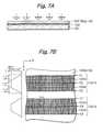
- FIGS. 6A, 7 A, 8 A, 9 A and 10 Aare cross-sectional views for explaining a method for forming a polycrystalline silicon layer on a glass substrate;
- FIGS. 6B, 7 B, 8 B, 9 B and 10 Bare plan views taken along the line A—A of FIGS. 6A, 7 A, 8 A, 9 A and 10 A, respectively;
- FIG. 11is a block circuit diagram illustrating a second embodiment of the system for manufacturing a semiconductor device according to the present invention.
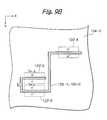
- FIG. 12is a diagram illustrating an example of the content of the manufacturing conduction file of FIG. 11;
- FIG. 13is a diagram illustrating an example of the recipe of FIG. 12;
- FIG. 14is a detailed block circuit diagram of the manufacturing management apparatus of FIG. 11.
- FIG. 15is a flowchart for explaining the operation of the manufacturing system of FIG. 11 .
- FIG. 1which illustrates a first embodiment of the present invention
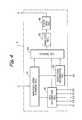
- reference numerals 11 , 12 , . . .designate customer terminals which are connected via the Internet 2 to a customer information management apparatus 3 .
- the customer information management apparatus 3is constructed by a plurality of manufacturing condition files 31 - 1 , 31 - 2 , . . . each corresponding to one of the customer terminals 11 , 12 , . . . , and recipe files 32 - 1 , 32 - 2 , . . . .
- the customer information management apparatus 3is connected via a communication line to a manufacturing management apparatus 4 , which will be explained later in detail.
- the manufacturing management apparatus 4is connected via a communication line to processing units such as a cleaning and rinsing unit 51 , a chemical vapor deposition (CVD) unit 52 , an exposure unit 53 , a developing unit 54 , a dry etching unit 55 and an inspection unit 56 .
- processing unitssuch as a cleaning and rinsing unit 51 , a chemical vapor deposition (CVD) unit 52 , an exposure unit 53 , a developing unit 54 , a dry etching unit 55 and an inspection unit 56 .
- FIG. 2which illustrates an example of the manufacturing condition file 31 - 1 of FIG. 1, the quantity, substrate, process specification and inspection specification for customer 1 are stored. Also, recipes of the process specification of FIG. 2 are stored in advance in the recipe files 32 - 1 , 32 - 2 , . . . , which correspond to the cleaning and rinsing process, the CVD process, . . . , respectively. An example of the recipe of the cleaning and rinsing process of FIG. 2 is illustrated in FIG. 3 . Further, a desired time for delivery is stored.
- the manufacturing management apparatus 4is constructed by a manufacturing planning section 41 for planning manufacturing of the semiconductor devices, a unit information section 42 for controlling the units 51 , 52 , . . . , 55 , an inspection information section 43 for controlling the unit 56 , a storing section 44 for storing information from the manufacturing planning section 41 , the unit information section 42 and the inspection information section 43 , an analysis section 45 for analyzing the content of the storing section 44 , and a state generating section 45 for generating the manufacturing state of the semiconductor devices in accordance with the analysis result of the analysis section 45 .
- the manufacturing planning section 41receives the content of the manufacturing condition files 31 - 1 , 31 - 2 , . . . , i.e., the name of lots, the designated process unit and the designated inspection units of the manufactured semiconductor devices, to make a manufacturing plan. For example, an estimated time for entry and an estimated time for delivery are calculated.
- the unit information section 42receives the name of lots and the designated processing units including the inspection unit from the manufacturing planing section 41 , to generate the start time and end time of each of the processing units for the lots.
- the unit information section 42is connected to the processing units 51 , 52 , . . . , 55 .
- the inspection information section 43receives the name of lots, the designated inspection units and the inspection specification from the manufacturing planning section 41 , to generate the inspection result.
- the inspection information section 43is connected to the inspection unit 56 .
- the start time and end time of each processing unit and the inspection result as well as the name of lotsare stored in the storing section 44 .
- a customeris logged-in by using an identification (ID) number and a password to the customer information management apparatus 3 .
- IDidentification
- the customer terminal 11is connected via the Internet 2 to the customer information management apparatus 3 .
- the customerreads its manufacturing condition file 31 - 1 and edits the content thereof with reference to the recipe files 32 - 1 , 32 - 2 , . . . , thus preparing an order.
- a desired time for deliverycan be written into the manufacturing condition file 31 - 1 .
- the manufacturing planning section 41calculates an estimated time for entry and an estimated time for delivery in accordance with the current state of the units 51 to 56 .
- the estimated entry time and delivery timeare stored in the storing section 44 , and then, are transmitted by the analysis section 45 and the state generating section 46 to the customer terminal 11 .
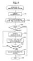
- step 503the customer decides whether the prepared order is to be proceeded with or to be cancelled. If the prepared order is to be proceeded with, the control proceeds to step 504 . On the other hand, if the prepared order is to be cancelled, the control proceeds directly to step 508 .
- the unit information section 42operates the units 51 to 55 , and also, the inspection information section 43 operates the unit 56 .
- the start time and end time of each of the units 51 to 55are transmitted from the unit information section 42 to the storing section 44 , and also, the inspection result, such as the thickness, the resistively or the depth is transmitted from the inspection information section 43 to the storing section 44 .
- the analysis section 45 and the state generating section 46are operated. That is, the analysis section 45 compares the start time and end time of each of the units 51 to 55 and the inspection result of the unit 56 with predetermined values supplied from the manufacturing planning section 41 , to generate the manufacturing state of the semiconductor devices, which is transmitted to the customer terminal 11 . If the estimated time for delivery is too delayed, a revised time for delivery is transmitted to the customer terminal 11 . Also, in this case, an alarm signal is transmitted to the customer terminal 11 .
- Step 506repeats the control at steps 504 and 505 until the semiconductor devices are completed.
- the completed semiconductor devicesare delivered to the customer, which is also informed to the customer terminal 11 .
- step 508the operation of FIG. 5 is completed by step 508 .
- FIGS. 6A, 6 B, 7 A, 7 B, 8 A, 8 B, 9 A, 9 B, 10 A and 10 Bare cross-sectional views taken along the line A—A of FIGS. 6B, 7 B, 8 B, 9 B and 10 B, respectively.
- the formation of this polycrystalline silicon layeris disclosed in the specification of U.S. Ser. No. 09/988,962 filed on Nov. 19, 2001.
- an about 0.5 to 1.1 mm thick glass substrate 101is subject to a cleaning and rinsing process to remove contaminants from the surface of the glass substrate 101 .
- an about 1 ⁇ m thick substrate covering layer 102 made of silicon oxideis deposited on the glass substrate 101 by a low pressure CVD (LPCVD) process using silane gas and oxygen gas.
- LPCVDlow pressure CVD
- an about 60 to 80 nm thick amorphous silicon layer 103is deposited on the substrate covering layer 102 by an LPCVD process using disilane gas at a temperature of about 500° C.
- the hydrogen concentration of the amorphous silicon layer 103is less than 1 atom percent to prevent the emission of hydrogen atoms from the amorphous silicon layer 103 by a laser irradiation process which will be carried out later. If a large number of hydrogen atoms are emitted from the amorphous silicon layer 103 , the surface of a polycrystalline silicon layer converted therefrom greatly fluctuates.
- the glass substrate 101is again subject to a cleaning and rinsing process to remove contaminants from the surface of the amorphous silicon layer 103 .
- the glass substrate 101is entered into a step and repetitive pulse laser apparatus where the amorphous silicon layer 103 is irradiated with laser line beams under an atmosphere of pure nitrogen gas at about 700 Torr (8.33 ⁇ 10 4 Pa).
- the laser line beamshave a rectangular size of 5 ⁇ m ⁇ 100 ⁇ m.
- the energy of the laser beamsis relatively high, for example, about 400 to 900 mJ/am 2 , and also, the slope of the energy with respect to the Y-direction is relatively sharp.
- the growth of polycrystalline silicon stops at YY 3 and Y 3 ′.
- polycrystalline silicon layer 103 ′A and 103 ′Bare obtained to include elongated grains having a length of approximately half of the width of the laser line beams.
- the polycrystalline silicon layer 103 ′A( 103 ′B) has stripes each of which is divided into two regions 1031 A and 1032 A ( 1031 B and 1032 B). Then, nitrogen is exhausted from the pulse laser apparatus, and then, oxygen gas is introduced there into.
- the manufacturing conditions for the polycrystalline silicon layers 103 ′A and 103 ′Bcan be different from each other.
- an about 10 nm thick gate insulating layer 104 - 1 made of silicon oxideis deposited on the entire surface by a plasma CVD process using silane gas, helium gas and oxygen gas at a temperature of about 350° C. Thereafter, as occasion demands, a hydrogen plasma process and an annealing process are carried out. Then, the gate insulating layer 104 - 1 and the polycrystalline silicon layer 103 ′A and 103 ′B are patterned by a photolithography and etching process, so that islands formed by the gate insulating layer 104 - 1 and the polycrystalline silicon layer 103 ′A and 103 ′B are formed. In this case, the sides of the islands ( 103 ′A, 103 ′B, 104 - 1 ) are tapered to suppress gate leakage currents. However, the gate insulating layer 104 - 1 can be deleted.
- the glass substrate 101is again subject to a cleaning and rinsing process to remove contaminants from the surface of the gate insulating layer 104 - 1 and the like. Then, an about 30 nm thick gate insulating layer 104 - 2 made of silicon oxide is deposited on the entire surface by a plasma CVD process using silane gas and oxygen gas at a temperature of about 450° C.
- gate electrode layer 105 - 1made of phosphorus-doped polycrystalline silicon is deposited on the gate insulating layer 104 - 2 by a plasma CVD process or an LPCVD process, and an about 110 nm thick gate electrode layer 105 - 2 made of tungsten silicide is deposited on the gate electrode layer 105 - 1 by a sputtering process. Then, the gate electrode layers 105 - 1 and 105 - 2 are patterned by a photolithography and etching process.
- impurity ionsare implanted into the polycrystalline silicon islands 103 ′A and 103 ′B in self-alignment with the patterned gate electrode layers 105 - 1 and 105 - 2 .
- impurity ionsare of an n-type
- source regions S and drain regions D of an n + -typeare formed within the polycrystalline silicon islands 103 ′A and 103 ′B.
- the impurity ionsare of a p-type
- source regions S and drain regions D of a p + -typeare formed within the polycrystalline silicon islands 103 ′A and 103 ′B.
- undoped regions of the polycrystalline silicon islands 103 ′A and 103 ′Bserve as channel regions C.
- a passivation layer 106 made of silicon oxideis deposited on the entire surface by a plasma CVD process using tetra-ethoxysilane (TEOS)gas and oxygen gas.
- TEOStetra-ethoxysilane
- contact holes CONTare perforated in the gate insulating layers 104 - 1 and 104 - 2 and the passivation layer 106 by a photolithography and etching process thereupon.
- a metal layer 107 made of aluminum, aluminum alloy, copper, copper alloy or refractory metal such as tungsten or molybdenumis deposited on the entire surface by a sputterning process or the like, and the metal layer 107 is patterned by a photolithography and etching process.
- CMOS inverteris formed by a P-channel TFT and two N-channel TFTs.
- the irradiation of laser line beams to the amorphous silicon layer 103can be carried out by using alignment marks.
- the alignment marks made of tungsten silicide or the likeare formed on the substrate covering layer 102 before the irradiation of laser beams to the amorphous silicon layer 103 .
- alignment marksare formed on the amorphous silicon layer 103 simultaneously with the irradiation of laser line beams to the amorphous silicon layer 103 .
- the patterning of the polycrystalline silicon layers 103 ′A and 103 ′B into the islandsis carried out by using the above-mentioned alignment marks.
- FIG. 11which illustrates a second embodiment of the present invention
- the polycrystalline silicon layers 103 ′A and 103 ′B of FIGS. 6A, 6 B, . . . , 10 A and 10 Bare formed.
- reference numerals 11 ′, 12 ′, . . .designate customer terminals which are connected via the Internet 2 ′ to a customer information management apparatus 3 ′.
- the customer information management apparatus 3 ′is constructed by a plurality of manufacturing condition files 31 ′- 1 , 31 ′- 2 , . . . each corresponding to one of the customer terminals 11 ′, 12 ′, . . . , and recipe files 32 ′- 1 , 32 ′- 2 , . . . .
- the customer information management apparatus 3is connected via a communication line to a manufacturing management apparatus 4 ′, which will be explained later in detail.
- the manufacturing management apparatus 4 ′is connected via a communication line to processing units such as a cleaning and rinsing unit 51 ′, an LPCVD unit 52 ′, crystallizing units 53 ′, 54 ′, 55 ′ and an inspection unit 56 ′.
- processing unitssuch as a cleaning and rinsing unit 51 ′, an LPCVD unit 52 ′, crystallizing units 53 ′, 54 ′, 55 ′ and an inspection unit 56 ′.
- FIG. 12which illustrates an example of the manufacturing condition file 31 ′- 1 of FIG. 11, the quantity, glass substrate, process specification and inspection specification for customer 1 are stored. Also, recipes of the process specification of FIG. 2 are stored in advance in the recipe files 32 ′- 1 , 32 ′- 2 , 32 ′- 3 , . . . , which correspond to the cleaning and rinsing process, the LPCVD process, the crystallizing process . . . , respectively. An example of the recipe of the crystallizing process of FIG. 12 is illustrated in FIG. 13 . Further, a desired time for delivery is stored.
- FIG. 14which is a detailed block circuit diagram of the manufacturing management apparatus 4 ′ of FIG. 11, the manufacturing management apparatus 4 ′ is constructed by a manufacturing planning section 41 ′ for planning manufacturing of the polycrystalline silicon layers, a unit information section 42 ′ for controlling the units 51 ′, 52 ′, . . .
- an inspection information section 43 ′for controlling the unit 56 ′
- a storing section 44 ′for storing information from the manufacturing planning section 41 ′, the unit information section 42 ′ and the inspection information section 43 ′
- an analysis section 45 ′for analyzing the content of the storing section 44 ′
- a state generating section 45 ′for generating the manufacturing state of the polycrystalline silicon layers in accordance with the analysis result of the analysis section 45 ′.
- the manufacturing planning section 41 ′receives the content of the manufacturing condition files 31 ′- 1 , 31 ′- 2 , . . . , i.e., the name of lots, the designated process unit and the designated inspection units of the manufactured polycrystalline silicon layers, to make a manufacturing plan. For example, an estimated time for entry and an estimated time for delivery are calculated.
- the unit information section 42 ′receives the name of lots and the designated processing units including the inspection unit from the manufacturing planning section 41 ′, to generate the start time and end time of each of the processing units for the lots.
- the unit information section 42 ′is connected to the processing units 51 ′, 52 ′, . . . , 55 ′.
- the inspection information section 43 ′receives the name of lots, the designated inspection units and the inspection specification from the manufacturing planning section 41 ′, to generate the inspection result.
- the inspection information section 43 ′is connected to the inspection unit 56 ′.
- the start time and end time of each processing unit and the inspection result as well as the name of lotsare stored in the storing section 44 ′.
- a customeris logged-in by using an ID number and a password to the customer information management apparatus 3 ′.
- the customer terminal 11 ′is connected via the Internet 2 ′ to the customer information management apparatus 3 ′.
- the customerreads its manufacturing condition file 31 ′- 1 and edits the content thereof with reference to the recipe files 32 ′- 1 , 32 ′- 2 , . . . , thus preparing an order.
- a desired time for deliverycan be written into the manufacturing condition file 31 ′- 1 .
- the manufacturing planning section 41 ′calculates an estimated time for entry and an estimated time for delivery in accordance with the current state of the units 51 ′ to 56 ′.
- the estimated entry time and delivery timeare stored in the storing section 44 ′, and then, are transmitted by the analysis section 45 ′ and the state generating section 46 ′ to the customer terminal 11 ′.
- step 1503the customer decides whether the prepared order is to be proceeded with or to be cancelled. If the prepared order is to be proceeded with, the control proceeds to step 1504 . On the other hand, if the prepared order is to be cancelled, the control proceeds directly to step 1508 .
- the unit information section 42 ′operates the units 51 ′ to 55 ′, and also, the inspection information section 43 ′ operates the unit 56 ′.
- the start time and end time of each of the units 51 ′ to 55 ′are transmitted from the unit information section 42 ′ to the storing section 44 ′, and also, the inspection result, such as the thickness or the deviation of laser irradiation is transmitted from the inspection information section 43 ′ to the storing section 44 ′.
- the analysis section 45 ′ and the state generating section 46 ′are operated. That is, the analysis section 45 ′ compares the start time and end time of each of the units 51 ′ to 55 ′ and the inspection result of the unit 56 ′ with predetermined values supplied from the manufacturing planning section 41 ′, to generate the manufacturing state of the polycrystalline silicon layers, which is transmitted to the customer terminal 11 ′. If the estimated time for delivery is too delayed, a revised time for delivery is transmitted to the customer terminal 11 ′. Also, in this case, an alarm signal is transmitted to the customer terminal 11 ′.
- Step 1506repeats the control at steps 1504 and 1505 until the polycrystalline silicon layers are completed.
- the completed glass substrate with the polycrystalline silicon layersare delivered to the customer, which is also informed to the customer terminal 11 ′.
- step 1508the operation of FIG. 15 is completed by step 1508 .
- the manufacturing efficiencycan be enhanced.
Landscapes
- Business, Economics & Management (AREA)
- Engineering & Computer Science (AREA)
- Finance (AREA)
- Accounting & Taxation (AREA)
- Physics & Mathematics (AREA)
- General Physics & Mathematics (AREA)
- Strategic Management (AREA)
- General Business, Economics & Management (AREA)
- Theoretical Computer Science (AREA)
- Marketing (AREA)
- Economics (AREA)
- Development Economics (AREA)
- Condensed Matter Physics & Semiconductors (AREA)
- Manufacturing & Machinery (AREA)
- Computer Hardware Design (AREA)
- Automation & Control Theory (AREA)
- Microelectronics & Electronic Packaging (AREA)
- Power Engineering (AREA)
- Recrystallisation Techniques (AREA)
- Management, Administration, Business Operations System, And Electronic Commerce (AREA)
- General Factory Administration (AREA)
Abstract
Description
Claims (17)
Applications Claiming Priority (2)
| Application Number | Priority Date | Filing Date | Title |
|---|---|---|---|
| JP2001247238AJP5318308B2 (en) | 2001-08-16 | 2001-08-16 | Semiconductor substrate production system |
| JP2001-247238 | 2001-08-16 |
Publications (2)
| Publication Number | Publication Date |
|---|---|
| US20030036971A1 US20030036971A1 (en) | 2003-02-20 |
| US6801826B2true US6801826B2 (en) | 2004-10-05 |
Family
ID=19076621
Family Applications (1)
| Application Number | Title | Priority Date | Filing Date |
|---|---|---|---|
| US10/202,045Expired - Fee RelatedUS6801826B2 (en) | 2001-08-16 | 2002-07-25 | System and method for manufacturing semiconductor devices controlled by customer |
Country Status (2)
| Country | Link |
|---|---|
| US (1) | US6801826B2 (en) |
| JP (1) | JP5318308B2 (en) |
Cited By (11)
| Publication number | Priority date | Publication date | Assignee | Title |
|---|---|---|---|---|
| US20050085017A1 (en)* | 2002-01-29 | 2005-04-21 | Tatsuo Ito | Semiconductor wafer manufacturing method, semiconductor wafer mnaufacturing order acceptance method, and semiconductor wafer manufacturing order acceptance system |
| US20050177269A1 (en)* | 2002-07-03 | 2005-08-11 | Tokyo Electron Limited | Method for dynamic sensor configuration and runtime execution |
| US20050256602A1 (en)* | 2004-05-11 | 2005-11-17 | Taiwan Semiconductor Manufacturing Co., Ltd. | System and method for customized tape-out requests for integrated circuit manufacturing |
| US20060100936A1 (en)* | 2004-11-05 | 2006-05-11 | Fujitsu Limited | Requirement management device, requirement management method, computer product |
| US20070061049A1 (en)* | 2005-09-12 | 2007-03-15 | Toshikatsu Masuda | System, method and program for designing a utility facility and method for manufacturing a product by the utility facility |
| US20080275793A1 (en)* | 2002-06-14 | 2008-11-06 | Edwin Hathaway | Method, apparatus and system for selecting, ordering and purchasing glass products |
| US20080306615A1 (en)* | 2006-02-07 | 2008-12-11 | Tokyo Electron Limited | Control device of substrate processing apparatus and control program therefor |
| US20090149967A1 (en)* | 2007-12-04 | 2009-06-11 | Siemens Aktiengesellschaft | Management System for Operation Items Used in Manufacturing |
| US20090177413A1 (en)* | 2002-08-02 | 2009-07-09 | Hidetoshi Nishiyama | System For Monitoring Foreign Particles, Process Processing Apparatus And Method Of Electronic Commerce |
| US20090241056A1 (en)* | 2008-03-21 | 2009-09-24 | Augustine Nancy L | Systems and methods for display and modification of information related to multiple businesses |
| US11291357B2 (en) | 2011-12-13 | 2022-04-05 | Endochoice, Inc. | Removable tip endoscope |
Families Citing this family (8)
| Publication number | Priority date | Publication date | Assignee | Title |
|---|---|---|---|---|
| JP2001326151A (en)* | 2000-05-16 | 2001-11-22 | Nec Corp | Semiconductor integrated circuit manufacturing system |
| JP4543788B2 (en)* | 2004-07-05 | 2010-09-15 | Jfeスチール株式会社 | Product inspection system and inspection method |
| JP2007157973A (en)* | 2005-12-05 | 2007-06-21 | Fujitsu Ltd | Semiconductor device manufacturing process control system and semiconductor device manufacturing process control method |
| US7571019B2 (en)* | 2005-12-30 | 2009-08-04 | Intel Corporation | Integrated configuration, flow and execution system for semiconductor device experimental flows and production flows |
| US20090326697A1 (en)* | 2006-11-17 | 2009-12-31 | Hejian Technology (Suzhou) Co., Ltd. | Semiconductor manufacturing automation system and method for using the same |
| JP5089492B2 (en)* | 2008-06-02 | 2012-12-05 | 株式会社日立製作所 | Client device introduction management system, client device introduction management method, information processing apparatus, and program |
| JP6763885B2 (en) | 2015-02-20 | 2020-09-30 | 4シー メディカル テクノロジーズ,インコーポレイテッド | Devices, systems and methods for cardiac treatment |
| JP7030005B2 (en)* | 2018-04-12 | 2022-03-04 | 株式会社ディスコ | Processing equipment |
Citations (16)
| Publication number | Priority date | Publication date | Assignee | Title |
|---|---|---|---|---|
| US5294811A (en)* | 1990-11-30 | 1994-03-15 | Hitachi, Ltd. | Thin film semiconductor device having inverted stagger structure, and device having such semiconductor device |
| JPH06268043A (en) | 1993-03-17 | 1994-09-22 | Nec Yamagata Ltd | Reticle arrangement |
| JPH06268067A (en) | 1993-03-16 | 1994-09-22 | Dainippon Printing Co Ltd | CAD system for LSI design |
| JPH09180980A (en) | 1995-12-21 | 1997-07-11 | Mitsubishi Electric Corp | Semiconductor device manufacturing system |
| JPH10247616A (en) | 1997-03-04 | 1998-09-14 | Canon Inc | Exposure apparatus, semiconductor production system and semiconductor manufacturing method |
| JPH11219875A (en) | 1998-01-30 | 1999-08-10 | Hitachi Ltd | Semiconductor manufacturing method and semiconductor manufacturing system |
| US6265290B1 (en)* | 1998-10-20 | 2001-07-24 | Samsung Electronics Co., Ltd. | Method for fabricating a thin film transistor and a substrate and thin film transistor manufactured using the same |
| US20010044667A1 (en)* | 2000-05-16 | 2001-11-22 | Nec Corporation | System of manufacturing semiconductor intergrated circuit |
| US20010051886A1 (en)* | 2000-05-31 | 2001-12-13 | Kunihiro Mitsutake | Electronic commerce method for semiconductor products, electronic commerce thereof, production system, production method, production equipment design system, production equipment design method, and production equipment manufacturing method |
| US20020107813A1 (en)* | 2000-06-08 | 2002-08-08 | Keisuke Kanatani | Manufacturing status indicating system |
| US20020111708A1 (en)* | 2001-01-22 | 2002-08-15 | Minoru Nakano | System for supplying semiconductor manufacturing system control programs |
| US20020123818A1 (en)* | 2001-03-01 | 2002-09-05 | Nec Corporation | Production managing system of semiconductor device |
| US20020143656A1 (en)* | 2001-03-30 | 2002-10-03 | Kabushiki Kaisha Toshiba | Method, system and program product for trading electronic products |
| US20030055736A1 (en)* | 2001-09-17 | 2003-03-20 | Formfactor, Inc. | Method and system for designing a probe card |
| US6578174B2 (en)* | 2001-06-08 | 2003-06-10 | Cadence Design Systems, Inc. | Method and system for chip design using remotely located resources |
| US20030208448A1 (en)* | 2002-03-12 | 2003-11-06 | Stuart Perry | Data brokering system for integrated remote tool access, data collection, and control |
- 2001
- 2001-08-16JPJP2001247238Apatent/JP5318308B2/ennot_activeExpired - Fee Related
- 2002
- 2002-07-25USUS10/202,045patent/US6801826B2/ennot_activeExpired - Fee Related
Patent Citations (17)
| Publication number | Priority date | Publication date | Assignee | Title |
|---|---|---|---|---|
| US5294811A (en)* | 1990-11-30 | 1994-03-15 | Hitachi, Ltd. | Thin film semiconductor device having inverted stagger structure, and device having such semiconductor device |
| JPH06268067A (en) | 1993-03-16 | 1994-09-22 | Dainippon Printing Co Ltd | CAD system for LSI design |
| JPH06268043A (en) | 1993-03-17 | 1994-09-22 | Nec Yamagata Ltd | Reticle arrangement |
| JPH09180980A (en) | 1995-12-21 | 1997-07-11 | Mitsubishi Electric Corp | Semiconductor device manufacturing system |
| JPH10247616A (en) | 1997-03-04 | 1998-09-14 | Canon Inc | Exposure apparatus, semiconductor production system and semiconductor manufacturing method |
| JPH11219875A (en) | 1998-01-30 | 1999-08-10 | Hitachi Ltd | Semiconductor manufacturing method and semiconductor manufacturing system |
| US6265290B1 (en)* | 1998-10-20 | 2001-07-24 | Samsung Electronics Co., Ltd. | Method for fabricating a thin film transistor and a substrate and thin film transistor manufactured using the same |
| US20010044667A1 (en)* | 2000-05-16 | 2001-11-22 | Nec Corporation | System of manufacturing semiconductor intergrated circuit |
| US20010051886A1 (en)* | 2000-05-31 | 2001-12-13 | Kunihiro Mitsutake | Electronic commerce method for semiconductor products, electronic commerce thereof, production system, production method, production equipment design system, production equipment design method, and production equipment manufacturing method |
| US20020107813A1 (en)* | 2000-06-08 | 2002-08-08 | Keisuke Kanatani | Manufacturing status indicating system |
| US20020111708A1 (en)* | 2001-01-22 | 2002-08-15 | Minoru Nakano | System for supplying semiconductor manufacturing system control programs |
| US20020123818A1 (en)* | 2001-03-01 | 2002-09-05 | Nec Corporation | Production managing system of semiconductor device |
| JP2002260977A (en)* | 2001-03-01 | 2002-09-13 | Nec Corp | Semiconductor device manufacture management system |
| US20020143656A1 (en)* | 2001-03-30 | 2002-10-03 | Kabushiki Kaisha Toshiba | Method, system and program product for trading electronic products |
| US6578174B2 (en)* | 2001-06-08 | 2003-06-10 | Cadence Design Systems, Inc. | Method and system for chip design using remotely located resources |
| US20030055736A1 (en)* | 2001-09-17 | 2003-03-20 | Formfactor, Inc. | Method and system for designing a probe card |
| US20030208448A1 (en)* | 2002-03-12 | 2003-11-06 | Stuart Perry | Data brokering system for integrated remote tool access, data collection, and control |
Cited By (33)
| Publication number | Priority date | Publication date | Assignee | Title |
|---|---|---|---|---|
| US7203559B2 (en)* | 2002-01-29 | 2007-04-10 | Shin-Etsu Handotai Co., Ltd. | Method for manufacturing semiconductor wafer, method for receiving order for manufacture of semiconductor wafer, and system for receiving order for manufacture of semiconductor wafer |
| US20050085017A1 (en)* | 2002-01-29 | 2005-04-21 | Tatsuo Ito | Semiconductor wafer manufacturing method, semiconductor wafer mnaufacturing order acceptance method, and semiconductor wafer manufacturing order acceptance system |
| US8255282B2 (en)* | 2002-06-14 | 2012-08-28 | Oldcastle Buildingenvelope, Inc. | Methods for selecting, ordering, and purchasing glass products |
| US7783525B2 (en)* | 2002-06-14 | 2010-08-24 | Oldcastle Glass, Inc. | Methods for selecting, ordering and purchasing glass products |
| US20120030058A1 (en)* | 2002-06-14 | 2012-02-02 | Edwin Hathaway | Methods for selecting, ordering, and purchasing glass products |
| US10290038B2 (en)* | 2002-06-14 | 2019-05-14 | Oldcastle Buildingenvelope, Inc. | Methods for selecting, ordering and purchasing glass products |
| US20120296766A1 (en)* | 2002-06-14 | 2012-11-22 | Oldcastle Buildingenvelope, Inc. | Methods for selecting, ordering and purchasing glass products |
| US20080275793A1 (en)* | 2002-06-14 | 2008-11-06 | Edwin Hathaway | Method, apparatus and system for selecting, ordering and purchasing glass products |
| US9767502B2 (en)* | 2002-06-14 | 2017-09-19 | Oldcastle Buildingenvelope, Inc. | Methods for selecting, ordering and purchasing glass products |
| US20140067616A1 (en)* | 2002-06-14 | 2014-03-06 | Oldcastle Buildingenvelope, Inc. | Methods for selecting, ordering and purchasing glass products |
| US8438071B2 (en)* | 2002-06-14 | 2013-05-07 | Oldcastle Buildingenvelope, Inc. | Methods for selecting, ordering and purchasing glass products |
| US7587343B2 (en)* | 2002-06-14 | 2009-09-08 | Oldcastle Glass, Inc. | Methods for selecting, ordering and purchasing glass products |
| US20100063900A1 (en)* | 2002-06-14 | 2010-03-11 | Edwin Hathaway | Methods for selecting, ordering and purchasing glass products |
| US20050177269A1 (en)* | 2002-07-03 | 2005-08-11 | Tokyo Electron Limited | Method for dynamic sensor configuration and runtime execution |
| US7636608B2 (en)* | 2002-07-03 | 2009-12-22 | Tokyo Electron Limited | Method for dynamic sensor configuration and runtime execution |
| US8045148B2 (en)* | 2002-08-02 | 2011-10-25 | Hitachi High-Technologies Corporation | System for monitoring foreign particles, process processing apparatus and method of electronic commerce |
| US20090177413A1 (en)* | 2002-08-02 | 2009-07-09 | Hidetoshi Nishiyama | System For Monitoring Foreign Particles, Process Processing Apparatus And Method Of Electronic Commerce |
| US20120002196A1 (en)* | 2002-08-02 | 2012-01-05 | Hidetoshi Nishiyama | System For Monitoring Foreign Particles, Process Processing Apparatus And Method Of Electronic Commerce |
| US8254662B2 (en)* | 2002-08-02 | 2012-08-28 | Hitachi High-Technologies Corporation | System for monitoring foreign particles, process processing apparatus and method of electronic commerce |
| US8620766B2 (en)* | 2003-06-06 | 2013-12-31 | Oldcastle Buildingenvelope, Inc. | Methods for selecting, ordering and purchasing glass products |
| US20130198041A1 (en)* | 2003-06-06 | 2013-08-01 | Oldcastle Buildingenvelope, Inc. | Methods for selecting, ordering and purchasing glass products |
| US7003362B2 (en)* | 2004-05-11 | 2006-02-21 | Taiwan Semiconductor Manufacturing Company, Ltd. | System and method for customized tape-out requests for integrated circuit manufacturing |
| US20050256602A1 (en)* | 2004-05-11 | 2005-11-17 | Taiwan Semiconductor Manufacturing Co., Ltd. | System and method for customized tape-out requests for integrated circuit manufacturing |
| US20060100936A1 (en)* | 2004-11-05 | 2006-05-11 | Fujitsu Limited | Requirement management device, requirement management method, computer product |
| US8355953B2 (en)* | 2004-11-05 | 2013-01-15 | Fujitsu Semiconductor Limited | Requirement management device, requirement management method, computer product |
| US7844433B2 (en)* | 2005-09-12 | 2010-11-30 | Kabushiki Kaisha Toshiba | System, method and program for designing a utility facility and method for manufacturing a product by the utility facility |
| US20070061049A1 (en)* | 2005-09-12 | 2007-03-15 | Toshikatsu Masuda | System, method and program for designing a utility facility and method for manufacturing a product by the utility facility |
| US7987012B2 (en)* | 2006-02-07 | 2011-07-26 | Tokyo Electron Limited | Control device of substrate processing apparatus and control program therefor |
| US20080306615A1 (en)* | 2006-02-07 | 2008-12-11 | Tokyo Electron Limited | Control device of substrate processing apparatus and control program therefor |
| US20090149967A1 (en)* | 2007-12-04 | 2009-06-11 | Siemens Aktiengesellschaft | Management System for Operation Items Used in Manufacturing |
| US9110460B2 (en)* | 2007-12-04 | 2015-08-18 | Siemens Aktiengesellschaft | Management system for operation items used in manufacturing |
| US20090241056A1 (en)* | 2008-03-21 | 2009-09-24 | Augustine Nancy L | Systems and methods for display and modification of information related to multiple businesses |
| US11291357B2 (en) | 2011-12-13 | 2022-04-05 | Endochoice, Inc. | Removable tip endoscope |
Also Published As
| Publication number | Publication date |
|---|---|
| JP5318308B2 (en) | 2013-10-16 |
| US20030036971A1 (en) | 2003-02-20 |
| JP2003059791A (en) | 2003-02-28 |
Similar Documents
| Publication | Publication Date | Title |
|---|---|---|
| US6801826B2 (en) | System and method for manufacturing semiconductor devices controlled by customer | |
| US8710507B2 (en) | Semiconductor thin film, thin film transistor, method for manufacturing same, and manufacturing equipment of semiconductor thin film | |
| US8041451B2 (en) | Method for bin-based control | |
| US20020103563A1 (en) | Method of manufacturing a semiconductor device and manufacturing system | |
| CN101536150B (en) | Server device and information processing method | |
| CN1744116B (en) | Method and system for semiconductor production automation | |
| JP2002260977A (en) | Semiconductor device manufacture management system | |
| US20020055207A1 (en) | Method for fabricating thin-film transistor | |
| US8095901B2 (en) | Method and system alerting an entity to design changes impacting the manufacture of a semiconductor device in a virtual fab environment | |
| US7203563B2 (en) | Automatic N2 purge system for 300 mm full automation fab | |
| CN1333312C (en) | Method and apparatus for scheduling production lots based on lot and tool health metrics | |
| CN101042997B (en) | Method and system for recessing a trench to target depth using feed forward data | |
| US20040038438A1 (en) | Method for reducing surface roughness of polysilicon films for liquid crystal displays | |
| US9008833B2 (en) | Dynamic routing control methods and systems for a cluster tool | |
| JP2006073845A (en) | Semiconductor manufacturing system | |
| US6678566B2 (en) | Backup control system (BCS) for optimizing utilization of multiple fabrication facilities | |
| JP2008034877A (en) | Semiconductor device manufacturing method and manufacturing system | |
| US7608475B2 (en) | Buffer layer for promoting electron mobility and thin film transistor having the same | |
| US6589825B2 (en) | Method for re-forming semiconductor layer in TFT-LCD | |
| JP2005277361A (en) | Process device control system and control method | |
| van Campen | Design of a multi-process multi-product wafer fab | |
| JP3216173B2 (en) | Method of manufacturing thin film transistor circuit | |
| KR100382021B1 (en) | Semiconductor device manufacturing method, manufacturing support system and manufacturing apparatus for manufacturing the same | |
| JPH11135797A (en) | Shape processing method of laminated film and method of manufacturing thin film transistor using the same | |
| KR20020086682A (en) | Thin film manufacturing method and manufacturing apparatus, and thin-film transistor and manufacturing method |
Legal Events
| Date | Code | Title | Description |
|---|---|---|---|
| AS | Assignment | Owner name:NEC CORPORATION, JAPAN Free format text:ASSIGNMENT OF ASSIGNORS INTEREST;ASSIGNOR:TANABE, HIROSHI;REEL/FRAME:013151/0329 Effective date:20020715 | |
| FEPP | Fee payment procedure | Free format text:PAYOR NUMBER ASSIGNED (ORIGINAL EVENT CODE: ASPN); ENTITY STATUS OF PATENT OWNER: LARGE ENTITY | |
| FPAY | Fee payment | Year of fee payment:4 | |
| FEPP | Fee payment procedure | Free format text:PAYER NUMBER DE-ASSIGNED (ORIGINAL EVENT CODE: RMPN); ENTITY STATUS OF PATENT OWNER: LARGE ENTITY | |
| AS | Assignment | Owner name:GETNER FOUNDATION LLC, DELAWARE Free format text:ASSIGNMENT OF ASSIGNORS INTEREST;ASSIGNOR:NEC CORPORATION;REEL/FRAME:026254/0381 Effective date:20110418 | |
| REMI | Maintenance fee reminder mailed | ||
| LAPS | Lapse for failure to pay maintenance fees | ||
| STCH | Information on status: patent discontinuation | Free format text:PATENT EXPIRED DUE TO NONPAYMENT OF MAINTENANCE FEES UNDER 37 CFR 1.362 | |
| FP | Lapsed due to failure to pay maintenance fee | Effective date:20121005 | |
| AS | Assignment | Owner name:VISTA PEAK VENTURES, LLC, TEXAS Free format text:ASSIGNMENT OF ASSIGNORS INTEREST;ASSIGNOR:GETNER FOUNDATION LLC;REEL/FRAME:045469/0164 Effective date:20180213 |