US6801784B1 - Continuous closed-loop power control system including modulation injection in a wireless transceiver power amplifier - Google Patents
Continuous closed-loop power control system including modulation injection in a wireless transceiver power amplifierDownload PDFInfo
- Publication number
- US6801784B1 US6801784B1US09/704,930US70493000AUS6801784B1US 6801784 B1US6801784 B1US 6801784B1US 70493000 AUS70493000 AUS 70493000AUS 6801784 B1US6801784 B1US 6801784B1
- Authority
- US
- United States
- Prior art keywords
- signal
- power
- power amplifier
- modulator
- phase
- Prior art date
- Legal status (The legal status is an assumption and is not a legal conclusion. Google has not performed a legal analysis and makes no representation as to the accuracy of the status listed.)
- Expired - Lifetime, expires
Links
Images


Classifications
- H—ELECTRICITY
- H04—ELECTRIC COMMUNICATION TECHNIQUE
- H04W—WIRELESS COMMUNICATION NETWORKS
- H04W52/00—Power management, e.g. Transmission Power Control [TPC] or power classes
- H04W52/04—Transmission power control [TPC]
- H04W52/52—Transmission power control [TPC] using AGC [Automatic Gain Control] circuits or amplifiers
- H—ELECTRICITY
- H03—ELECTRONIC CIRCUITRY
- H03F—AMPLIFIERS
- H03F1/00—Details of amplifiers with only discharge tubes, only semiconductor devices or only unspecified devices as amplifying elements
- H03F1/02—Modifications of amplifiers to raise the efficiency, e.g. gliding Class A stages, use of an auxiliary oscillation
- H03F1/0205—Modifications of amplifiers to raise the efficiency, e.g. gliding Class A stages, use of an auxiliary oscillation in transistor amplifiers
- H03F1/0261—Modifications of amplifiers to raise the efficiency, e.g. gliding Class A stages, use of an auxiliary oscillation in transistor amplifiers with control of the polarisation voltage or current, e.g. gliding Class A
- H03F1/0272—Modifications of amplifiers to raise the efficiency, e.g. gliding Class A stages, use of an auxiliary oscillation in transistor amplifiers with control of the polarisation voltage or current, e.g. gliding Class A by using a signal derived from the output signal
- H—ELECTRICITY
- H04—ELECTRIC COMMUNICATION TECHNIQUE
- H04W—WIRELESS COMMUNICATION NETWORKS
- H04W52/00—Power management, e.g. Transmission Power Control [TPC] or power classes
- H04W52/04—Transmission power control [TPC]
- H04W52/06—TPC algorithms
- H04W52/08—Closed loop power control
- H—ELECTRICITY
- H03—ELECTRONIC CIRCUITRY
- H03F—AMPLIFIERS
- H03F2200/00—Indexing scheme relating to amplifiers
- H03F2200/294—Indexing scheme relating to amplifiers the amplifier being a low noise amplifier [LNA]
- H—ELECTRICITY
- H03—ELECTRONIC CIRCUITRY
- H03F—AMPLIFIERS
- H03F2200/00—Indexing scheme relating to amplifiers
- H03F2200/372—Noise reduction and elimination in amplifier
- H—ELECTRICITY
- H04—ELECTRIC COMMUNICATION TECHNIQUE
- H04B—TRANSMISSION
- H04B1/00—Details of transmission systems, not covered by a single one of groups H04B3/00 - H04B13/00; Details of transmission systems not characterised by the medium used for transmission
- H04B1/02—Transmitters
- H04B1/04—Circuits
- H04B2001/0408—Circuits with power amplifiers
- H04B2001/0416—Circuits with power amplifiers having gain or transmission power control
Definitions
- This inventionrelates to the versatile transmission of radio frequency power in a wireless communication device transmitter, and more particularly, to a continuous closed-loop power control system including modulation injection into a wireless transceiver's power amplifier.
- the modulation schemecan be 8-quadrature phase shift keying (8QPSK), offset ⁇ /4 differential quadrature phase shift keying ( ⁇ /4 -DQPSK) or variations and the access format is time division multiple access (TDMA).
- TDMAtime division multiple access
- Other standardsmay require the use of, for example, code division multiple access (CDMA).
- GSMglobal system for mobile communications
- GMSKgaussian minimum shift keying
- a GMSK modulation schemesupplies a very clean phase modulated (PM) transmit signal to a non-linear power amplifier directly from an oscillator.
- a non-linear power amplifierwhich is highly efficient, can be used, thus allowing efficient transmission of the phase-modulated signal and minimizing power consumption.
- the modulated signalis supplied directly from an oscillator, the need for filtering, either before or after the power amplifier, is minimized.
- Other transmission standardssuch as that employed in IS-136, however, use a modulation scheme in which both a PM signal and an amplitude modulated (AM) signal are transmitted. Standards such as these increase the data rate without increasing the bandwidth of the transmitted signal.
- the power control loopWhen attempting to include a PM component and an AM component in a GSM type modulation system, the power control loop will attenuate the amplitude variations present in the signal in an attempt to maintain a constant output power. In such an arrangement, the power control loop tends to cancel the AM portion of the signal.
- the output powercan be controlled by applying a pre-determined control voltage to the power amplifier.
- a pre-determined control voltageto the power amplifier.
- the output powermay be controlled by a feedback loop having a time-constant that is very low compared to the time-constant of the amplitude variations of the modulator.
- Another known method to control the output poweris to “pre-distort” the modulated signal in such a way that the power control loop will cancel the effect of the pre-distortion.
- the amplitude informationis passed through a transfer function that is the inverse of the power control loop transfer function.
- Known multi-mode transmitter architecturesrequire multiple variable elements, which are chosen depending upon the desired transmit mode. These architectures are complex, unreliable, require periodic calibration, and cannot support multiple transmission standards without significant adjustments to the supporting analog and digital circuitry.
- a multi-band and multi-mode portable transceiverthat can transmit a signal containing both a PM component and an AM component, while maximizing the efficiency of the power amplifier. Furthermore, it would be desirable to have such a multi-band and multi-mode portable transceiver that can use conventional in-phase (I) and quadrature (Q) transmit signal components without requiring separate baseband signals for phase modulation and amplitude modulation. Further still, as the GSM standard evolves further, such as with the development of enhanced data rates for GSM evolution (EDGE), it is desirable to have one portable transceiver that may operate in all systems.
- EDGEenhanced data rates for GSM evolution
- the inventionprovides a continuous closed-loop power control system, which includes modulation injection into a wireless transceiver's power amplifier that allows the use of non-linear, power efficient amplifiers.
- the inventionuses a single continuous closed-loop power control system that allows an AM signal to be injected into the power amplifier through the power amplifier control port.
- the AM signalis derived from the output of an I/Q modulator and supplied to a comparator located within the power control feedback loop.
- FIG. 1is a block diagram illustrating a simplified portable transceiver.
- FIG. 2is a block diagram illustrating the upconverter and power control element of FIG. 1 including the continuous closed-loop power control system of the invention.
- FIG. 3is a graphical representation of the average power output of the power amplifier of FIG. 2 .
- FIG. 4is a schematic view illustrating an alternative embodiment of the power amplifier circuit of FIG. 2 .
- FIG. 5is a schematic view illustrating another alternative embodiment of the power amplifier circuit of FIG. 2 .
- the continuous closed-loop power control system including modulation injectioncan be implemented in any system where it is desirable to transmit a combined signal including a PM component and an AM component.
- the continuous closed-loop power control systemcan be implemented independently from the modulation injection, where both systems are applicable to any system where it is desirable to implement a closed power control feedback loop and where a PM signal and an AM signal are amplified by a power amplifier.
- the continuous closed-loop power control system including modulation injectioncan be implemented in software, hardware, or a combination of hardware and software.
- selected portions of the continuous closed-loop power control system including modulation injectionare implemented in hardware and software.
- the hardware portion of the inventioncan be implemented using specialized hardware logic.
- the software portioncan be stored in a memory and be executed by a suitable instruction execution system (microprocessor).
- the hardware implementation of the continuous closed-loop power control system including modulation injectioncan include any or a combination of the following technologies, which are all well known in the art: a discrete logic circuit(s) having logic gates for implementing logic functions upon data signals, an application specific integrated circuit having appropriate logic gates, a programmable gate array(s) (PGA), a field programmable gate array (FPGA), etc.
- a discrete logic circuit(s)having logic gates for implementing logic functions upon data signals
- an application specific integrated circuithaving appropriate logic gates
- PGAprogrammable gate array
- FPGAfield programmable gate array
- the continuous closed-loop power control system including modulation injection softwarewhich comprises an ordered listing of executable instructions for implementing logical functions
- modulation injection softwarewhich comprises an ordered listing of executable instructions for implementing logical functions
- any computer-readable mediumfor use by or in connection with an instruction execution system, apparatus, or device, such as a computer-based system, processor-containing system, or other system that can fetch the instructions from the instruction execution system, apparatus, or device and execute the instructions.
- a “computer-readable medium”can be any means that can contain, store, communicate, propagate, or transport the program for use by or in connection with the instruction execution system, apparatus, or device.
- the computer readable mediumcan be, for example but not limited to, an electronic, magnetic, optical, electromagnetic, infrared, or semiconductor system, apparatus, device, or propagation medium.
- the computer-readable mediumcould even be paper or another suitable medium upon which the program is printed, as the program can be electronically captured, via for instance optical scanning of the paper or other medium, then compiled, interpreted or otherwise processed in a suitable manner if necessary, and then stored in a computer memory.
- FIG. 1is a block diagram illustrating a simplified portable transceiver 100 .
- Portable transceiver 100includes speaker 102 , display 104 , keyboard 106 , and microphone 108 , all connected to baseband subsystem 110 .
- portable transceiver 100can be, for example but not limited to, a portable telecommunication handset such as a mobile cellular-type telephone.
- Speaker 102 and display 104receive signals from baseband subsystem 110 via connections 112 and 114 , respectively, as known to those skilled in the art.
- keyboard 106 and microphone 108supply signals to baseband subsystem 110 via connections 116 and 118 , respectively.
- Baseband subsystem 110includes microprocessor ( ⁇ P) 120 , memory 122 , analog circuitry 124 , and digital signal processor (DSP) 126 in communication via bus 128 .
- Bus 128though shown as a single bus, may be implemented using a number of busses connected as necessary among the subsystems within baseband subsystem 110 .
- Microprocessor 120 and memory 122provide the signal timing, processing and storage functions for portable transceiver 100 .
- Analog circuitry 124provides the analog processing functions for the signals within baseband subsystem 110 .
- Baseband subsystem 110provides control signals to radio frequency (RF) subsystem 130 via connection 132 .
- RFradio frequency
- control signalsmay originate from DSP 126 or from microprocessor 120 , and are supplied to a variety of points within RF subsystem 130 . It should be noted that, for simplicity, only the basic components of portable transceiver 100 are illustrated.
- Baseband subsystem 110also includes analog-to-digital converter (ADC) 134 and digital-to-analog converters (DACs) 136 and 142 .
- ADC 134 and DACs 136 and 142also communicate with microprocessor 120 , memory 122 , analog circuitry 124 and DSP 126 via bus 128 .
- DAC 136converts the digital communication information within baseband subsystem 110 into an analog signal for transmission to RF subsystem 130 via connection 140 .
- Connection 140while shown as two directed arrows, includes the information that is to be transmitted by RF subsystem 130 after conversion from the digital domain to the analog domain.
- DAC 136supplies baseband in-phase (I) and quadrature (Q) components of the information signal to be transmitted via connection 140 to modulator 146 .
- modulator 146is an I/Q modulator.
- DAC 142supplies control signals to various components with RF subsystem 130 via connection 132 .
- Modulator 146after receiving a frequency reference signal, also called a “local oscillator,” signal, or “LO,” from synthesizer 148 via connection 150 , modulates the I and Q information signals received from the DAC 136 onto the LO signal and provides a modulated signal via connection 152 to upconverter 154 .
- Modulator 146also supplies an intermediate frequency (IF) signal containing only the desired amplitude modulated (AM) signal component on connection. 138 for input to the power control element 300 via connection 138 .
- the power control element 300also supplies to the modulator 146 via connection 144 a constant level IF signal containing both the phase modulated (PM) and AM components of the transmit signal. The operation of the power control element 300 will be described below with reference to FIG. 2 .
- Upconverter 154also receives a frequency reference signal from synthesizer 148 via connection 156 .
- Synthesizer 148determines the appropriate frequency to which upconverter 154 will upconvert the modulated signal on connection 152 .
- Upconverter 154supplies the fully modulated signal at the appropriate transmit frequency via connection 158 to power amplifier 160 .
- Power amplifier 160amplifies the modulated signal on connection 158 to the appropriate power level for transmission via connection 162 to antenna 164 .
- switch 166controls whether the amplified signal on connection 162 is transferred to antenna 164 or whether a received signal from antenna 164 is supplied to filter 168 . The operation of switch 166 is controlled by a control signal from baseband subsystem 110 via connection 132 .
- a portion of the amplified transmit signal power on connection 162is supplied via connection 170 to power control element 300 .
- Power control element 300forms a continuous closed power control feedback loop and supplies an information signal on connection 172 instructing the power amplifier 160 as to the power to which the signal on connection 158 should be amplified.
- the power control element 300also receives the LO signal from synthesizer 148 via connection 198 . The operation of power control element 300 will be described in further detail with respect to FIG. 2 .
- a signal received by antenna 164may, at the appropriate time determined by baseband subsystem 110 , be directed via switch 166 to receive filter 168 .
- Receive filter 168will filter the received signal and supply the filtered signal on connection 174 to low noise amplifier (LNA) 176 .
- LNAlow noise amplifier
- Receive filter 168may be a bandpass filter that passes all channels of the particular cellular system where the portable transceiver 100 is operating. As an example, for a 900 MHz GSM system, receive filter 168 would pass all frequencies from 935.1 MHz to 959.9 MHz, covering all 124 contiguous channels of 200 kHz each. The purpose of this filter is to reject all frequencies outside the desired region.
- LNA 176amplifies the very weak signal on connection 174 to a level at which downconverter 178 can translate the signal from the transmitted frequency back to a baseband frequency.
- LNA 176 and downconverter 178can be accomplished using other elements, such as, for example but not limited to, a low noise block downconverter (LNB).
- LNBlow noise block downconverter
- Downconverter 178receives an LO signal from synthesizer 148 , via connection 180 .
- the LO signaldetermines the frequency to which to downconvert the signal received from LNA 176 via connection 182 .
- the downconverted frequencyis called the intermediate frequency (IF).
- Downconverter 178sends the downconverted signal via connection 184 to channel filter 186 , also called the “IF filter.”
- Channel filter 186filters the downconverted signal and supplies it via connection 188 to amplifier 190 .
- the channel filter 186selects the one desired channel and rejects all others. Using the GSM system as an example, only one of the 124 contiguous channels is actually to be received.
- the synthesizer 148determines the selected channel.
- Amplifier 190amplifies the received signal and supplies the amplified signal via connection 192 to demodulator 194 .
- Demodulator 194recovers the transmitted analog information and supplies a signal representing this information via connection 196 to ADC 134 .
- ADC 134converts these analog signals to a digital signal at baseband frequency and transfers it via bus 128 to DSP 126 for further processing.
- FIG. 2is a block diagram illustrating the upconverter 154 and power control element 300 of FIG. 1 including the continuous closed-loop power control system and modulation injection of the invention. Beginning with a description of the power control loop 300 , a portion of the output power present at the output of power amplifier 160 on connection 162 is diverted by coupler 222 via connection 170 and input to mixer 226 in the power control element 300 . Mixer 226 also receives the local oscillator (LO) signal from synthesizer 148 via connection 198 .
- LOlocal oscillator
- the mixer 226down converts the RF signal on connection 170 to an intermediate frequency (IF) signal on connection 228 .
- IFintermediate frequency
- mixer 226takes a signal having a an o frequency of approximately 2 gigahertz (GHz) on connection 170 and down converts it to a frequency of approximately 100 megahertz (MHz) on connection 228 for input to variable gain element 232 .
- Variable gain element 232can be, for example but not limited to, a variable gain amplifier or an attenuator. In such an arrangement, variable gain element 232 might have a dynamic range of approximately 70 decibels (dB) i.e., +35 dB/ ⁇ 35 dB.
- Variable gain element 232receives a control signal input from the non-inverting output of amplifier 236 via connection 234 .
- the input to amplifier 236is supplied via connection 132 from the DAC 142 of FIG. 1 .
- the signal on connection 132is a reference voltage signal for the transmit power level and provides the power profile.
- This signal on connection 132is supplied to a reconstruction filter, which includes resistor 240 and capacitor 242 . In this manner, a reference voltage for the transmit power level and power profile is supplied via connection 234 to the control input of the variable gain element 232 .
- variable gain element 232 on connection 246is at an IF and includes modulation having both an AM component and a PM component and is called the “power measurement signal.” This power measurement signal is related to the absolute output power of power amplifier 160 , and includes a very small error related to the AM and PM components present in the signal.
- the output of variable gain element 232 on connection 246is supplied to the input of power detector 262 and is also supplied to a limiter 248 in the phase locked loop 220 .
- the IF signal on connection 246includes both an AM component and a PM component.
- the signal on connection 246is supplied to power detector 262 , which provides, on connection 264 , a baseband signal representing the instantaneous level of IF power present on connection 246 .
- the output of power detector 262 on connection 264is supplied to the inverting input of amplifier 268 .
- Amplifier 268 , capacitor 266 and capacitor 270form a comparator 284 , which provides the error signal used to control the power amplifier 160 via connection 272 .
- the non-inverting input to the amplifier 268is supplied via connection 138 from the output of the modulator 146 through the power detector 276 .
- the signal on connection 138 supplied to the non-inverting input of amplifier 268contains the AM modulation developed by the modulator 146 in the phase locked loop 220 for input to the control port 172 of power amplifier 160 .
- the gain of the power control loop 300amplifies the signal on connection 272 such that the difference between the signals on connections 264 and 138 input to amplifier 268 provide an error on connection 272 that is used to control the output of the power amplifier 160 .
- the error on connection 272is supplied to variable gain element 274 , which can be similar in structure to variable gain element 232 . However, the variable gain element 274 has a function that is inverse to that of variable gain element 232 .
- the control input to variable gain element 274is supplied from the inverting output of amplifier 236 . In this manner, the power amplifier control signal on connection 172 supplied to the control port of power amplifier 160 drives the power amplifier 160 to provide the proper output on connection 162 .
- the level of the signal on connection 264 and the level of the signal on connection 138should be equal. For example, if the output level of the variable gain element 232 is increased by a factor of 10, then the level of the output of power amplifier 160 should be decreased accordingly to maintain equilibrium at the input of the amplifier 268 . The output of the power amplifier 160 changes to cancel the gain change of variable gain element 232 . In this manner, the amplitude of the signal on connection 264 remains equal to the amplitude of the signal on connection 138 . However, this implies that the signal on connection 228 lags the signal on connection 234 with the result that the two signals will not completely cancel. In this manner, an error signal with an AM and a PM portion is present on connection 246 .
- the signal on connection 246is converted by power detector 262 from an IF signal to a baseband signal on connection 264 .
- the signal on connection 264is amplified by amplifier 268 and amplifier 274 to drive the power amplifier control port on connection 172 so that the desired signal is achieved at the output of the power amplifier 160 on connection 162 .
- Power control loop 300has sufficient gain so that the error signal on connection 264 can be kept small. In such a case, the gain changes of variable gain element 232 and the power amplifier 160 will substantially be the inverse of each other.
- the amplifier 268In addition to amplifying the error signal on connection 264 , the amplifier 268 also compares the power measurement signal on connection 264 with a reference voltage signal including an AM portion on connection 138 , supplied by the modulator 146 within the phase locked loop 220 .
- the DC voltage level on connection 138affects the desired static output power for the power amplifier 268 , irrespective of AM modulation.
- Amplifier 268compares the signal level on connection 264 with the signal level on connection 138 and then amplifies the difference, thus providing a power control signal on connection 272 .
- the comparator 284functions as an integrator, which is also a low pass filter.
- the power control signal on connection 272drives the variable gain amplifier 274 , which corrects for the effect that variable gain element 232 has on the transfer function of power control loop 300 .
- the variable gains of variable gain element 232 and variable gain element 274are complimentary. Because the power measurement signal is present on connection 264 and the AM error signal is present on connection 138 , the amplifier 268 provides a dual function; (1) it amplifies the AM error signal on connection 138 so as to modulate the power output of power amplifier 160 via connection 172 to have the correct amount of AM; and (2) it performs the average power comparison and amplifies the result, thus providing a control signal on connection 272 that drives the power amplifier 160 to the correct average power output.
- both the AM error signal and the power control error signalare amplified to a level sufficient to drive the power amplifier 160 to the desired average power with the desired AM signal.
- the desired AM portion of the signalis supplied to the control input 172 of power amplifier 160 and made present on the power amplifier output on connection 162 .
- Mixer 226 , variable gain element 232 , power detector 262 , amplifier 268 and variable gain element 274provide a continuous closed-loop power control feedback system to control the power output of power amplifier 160 , while allowing for the introduction of the AM portion of the transmit signal via connection 138 .
- the continuous power-control feedback loopallows the correction of any phase shift caused by power amplifier 160 .
- the PLL 220now includes a feedback loop for looping back the output of power amplifier 160 to the input of phase/frequency detector 208 . Any unwanted phase shift generated by the power amplifier 160 will be corrected by the PLL 220 .
- the output of variable gain element 232passes any phase distortion present via connection 246 to limiter 248 for correction by the PLL 220 . As such, the phase of the output of power amplifier 160 is forced to follow the phase of the LO signal on connection 156 .
- variable gain element 232In order to remove the AM from the output of variable gain element 232 , the variable gain element 232 is connected via connection 246 and connection 144 to the input of limiter 248 . Limiter 248 develops a local oscillator signal containing only a PM component on connection 250 . This LO signal is supplied via connection 250 to the modulator 146 .
- the baseband I and Q information signalsare supplied via connections 278 and 282 , respectively, to the modulator 146 .
- the I and Q baseband information signal interfaceis understood by those having ordinary skill in the art.
- the output on connection 252is an intermediate frequency signal including an AM component in the form of an AM reference signal and a small PM error signal.
- the output of modulator 146is supplied via connection 252 to power detector 276 .
- the output of power detector 276also includes the AM portion of the desired transmit signal.
- the signal provided on connection 138is a reference signal for input to the power control loop 300 . Because the power control loop 300 has limited bandwidth, the rate at which the amplitude modulation occurs on connection 13 . 8 is preferably within that power control loop bandwidth.
- the output of limiter 248is supplied via connection 250 as a local oscillator signal having a PM component, but substantially no AM component to the modulator 146 .
- the modulator 146removes virtually the entire PM component and applies an AM modulated component to the signal and supplies this signal via connection 252 .
- the I and Q signalsare reversed on connections 278 and 282 , respectively. In this manner, the output of modulator 146 on connection 252 contains a very small PM portion and a significant AM portion.
- the modulator 146acts as a comparator, comparing the I and Q signals on connections 278 and 282 , respectively, with the LO signal supplied from the output of the variable gain element 232 , through limiter 248 and on connection 250 .
- the components within the phase locked loop 220provide gain for the comparison of the PM on connection 250 and the modulator connections 278 and 282 , thus providing a phase error output of the modulator 146 on connection 252 .
- This phase error signalis then supplied to limiter 256 , which outputs a signal on connection 258 containing the small PM phase error component.
- a feedback signal taken from the output of variable gain element 232 on connection 246is supplied as continuous feedback to the phase locked loop 220 .
- the error signal output of modulator 146 on connection 252 containing the phase errorwill get smaller and smaller as the gain of the phase locked loop 220 increases. However, there will always be some error signal present, thus enabling the phase locked loop 220 to achieve phase lock.
- a single feedback loopcan be used to continuously control the output power of power amplifier 160 from the time that the amplifier is off through the time when the amplifier 160 is providing full output power.
- Phase/frequency detector 208receives an unmodulated input signal from synthesizer 148 via connection 156 .
- the unmodulated input signalis frequency divided by a number “x” in order to provide a signal having an appropriate frequency on connection 204 .
- the number “x”is chosen so as to minimize the design complexity of the synthesizer 148 and can be, for example, but not limited to, chosen to convert the output of the synthesizer 148 to a frequency of 100 MHz.
- Phase/frequency detector 208also receives the output of divider 260 via connection 206 .
- Phase/frequency detector 208detects any phase difference between the signal on connection 204 and the signal on connection 206 and places a signal on connection 210 that has an amplitude proportional to the difference. When the phase difference reaches 360°, the output of phase/frequency detector 208 on connection 210 will become proportional to the frequency difference between the signals on connections 204 and 206 .
- phase/frequency detector 208 on connection 210is a digital signal having a value of either a 0 or a 1 with a very small transition time between the two output states.
- This signal on connection 210is supplied to low-pass filter 212 , which integrates the signal on connection 210 and places a DC signal on connection 214 that controls the frequency of the transmit voltage control oscillator (TX VCO) 216 .
- the output of TX VCO 216is supplied via connection 158 directly to the power amplifier 160 .
- the synthesizer 148 , limiter 248 , modulator 146 , limiter 256 , divider 260 , divider 202 , phase/frequency detector 208 , low-pass filter 212 and TX VCO 216form a phase locked loop (PLL) 200 , which is used to determine the transmit frequency on connection 158 .
- PLLphase locked loop
- the two signals entering the phase/frequency detector 208 on connections 204 and 206have precisely the same phase and frequency, and the output of the phase/frequency detector 208 on connection 210 goes to zero.
- the output of the integrating low-pass filter 212 on connection 214stabilizes, resulting in a fixed frequency out of TX VCO 216 .
- the synthesizer 148 and the mixer 226ensure that the frequency of the signal output from the TX VCO 216 on connection 158 tracks the sum of the frequencies of the local oscillator signal supplied by synthesizer 148 and the IF frequency on connection 206 .
- phase locked loop 220When the phase locked loop 220 is locked, the phase of the signal on connection 204 and the phase of the signal on connection 206 will be equal. Because the amount of PM on connection 206 should be very small, the gain in the phase locked loop 220 has to be sufficiently high to amplify the error signal on connection 206 to a level at which the phase/frequency detector 208 can make a comparison.
- the modulator 146By using the modulator 146 to impose the I and Q information signals on the signal on connection 250 in a direction opposite from which it is desirable for the phase of the TX VCO to move, and because it is desirable for the phase locked loop 220 to remain locked, the phase of the signal output from the TX VCO 216 on connection 158 will move opposite that of the phase imposed by the modulator 146 . In this manner, the PM error signal present on connection 206 is minimized by the very high sensitivity, of the order of many MHz per volt, of the TX VCO 216 .
- the power control loop 300is a closed loop for AM signals at connection 138 , it is possible to use a non-linear, and therefore highly efficient, power amplifier 160 . Furthermore, the undesirable and detrimental AM-to-PM conversion, which occurs due to the amplitude dependence of an amplifier's phase shift, is rectified by the power amplifier 160 being included within the phase locked loop 220 . By separating the AM and the PM modulation and by providing closed loop control for both the AM and PM modulation, a non-linear, and therefore highly efficient power amplifier can be used.
- the power amplifier 160In some applications it is desirable to allow the power amplifier 160 to output a signal containing both an AM component and a PM component, while maintaining the power amplifier 160 as a non-linear (and therefore highly efficient) power amplifier.
- the output of modulator 146will include both a very small AM and PM component, with limiter 256 used to cancel the AM component present on connection 252 , thereby preventing any AM-to-PM conversion in the phase/frequency detector 208 .
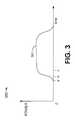
- FIG. 3is a graphical representation of the average power output of power amplifier 160 of FIG. 2 .
- the vertical axis of graph 350represents average power output of the power amplifier 160 and the horizontal axis of graph 350 represents time.
- Point “a”represents the point in time at which a transmission burst is initiated.
- leakage from the power amplifier 160is used to provide feedback from the variable gain element 232 (FIG. 2) to the phase locked loop 220 (FIG. 2) with the variable gain element 232 set to maximum gain.
- the point “c” in FIG. 3represents the point at which the power amplifier 160 has developed sufficient power so that transmission of data may begin. In this manner, a single power control loop provides continuous power detection and feedback to the PLL 220 .
- FIG. 4is a schematic view illustrating an alternative embodiment 400 of the power amplifier circuit of FIG. 2 .
- the power amplifier circuit 400 of FIG. 4includes a mixer 492 added to the phase locked loop 420 .
- the mixer 492receives the output of the TX VCO 416 on connection 494 and also receives as input the output of a low-pass filter 490 via connection 496 .
- the output of modulator 446 on connection 452is supplied to mixer 480 .
- Mixer 480combines the PM component of the signal on connection 458 with the AM component of the signal on connection 452 .
- the mixer 480combines the signal on connection 452 containing the AM and very small PM component and the signal on connection 458 containing the very small PM component, and combines them, thus extracting the AM signal and placing it on connection 484 .
- the AM signal on connection 484is at a baseband frequency and is supplied to amplifier 486 .
- Amplifier 486scales the signal on connection 484 and supplies the scaled signal, via connection 488 , to low-pass filter 490 .
- the AM slope informationis supplied to the control input to the amplifier 486 from the DAC 142 via connection 132 (FIG. 1 ).
- Low-pass filter 490removes any high frequency components from the signal on connection 488 and supplies the AM signal via connection 496 to the mixer 492 .
- the mixer 492combines the AM signal on connection 496 with the PM signal supplied from the TX VCO 416 on connection 494 and supplies a combined modulated signal containing both AM and PM on connection 458 . This combined signal is then supplied to the power amplifier 160 .
- a reference voltage signal containing the AM signal componentis supplied from the output of the modulator 446 via connection 438 to the non-inverting input of amplifier 468 in the comparator 484 .
- the signal supplied from power detector 462 via connection 464contains an AM component. Because the AM signal component on connection 464 is in phase with respect to the AM signal component on connection 438 , the two AM components will substantially cancel in the comparator 484 , thus eliminating the AM portion of the signal from the output of amplifier 468 on connection 472 .
- the output of amplifier 468 on connection 472is the error signal used to adjust the output power of power amplifier 160 as described above.
- FIG. 5is a schematic view illustrating another alternative embodiment 500 of the power amplifier circuit of FIG. 2 .
- the power amplifier circuit 500includes power control loop 500 , where modulator 546 is placed at the output of variable gain element 532 .
- the input signal to modulator 546 on connection 538is a constant level signal supplied by variable gain element 532 .
- the output of variable gain element 532includes both an AM and PM component.
- the baseband I and Q information signalsare supplied to the modulator 546 via connections, 578 and 582 , respectively.
- the I and Q componentswill remove, or greatly reduce the level of the PM signal on connection 538 within the loop bandwidth of phase locked loop 520 .
- the I and Q portionswill also reduce the AM component by a function equal to the gain of the power control loop 500 . Therefore, the value of the AM and PM components at the output of modulator 546 on connection 550 are very small error signals as mentioned above.
- the inverse of the I and Q information signalsare supplied to the modulator 546 on connections 578 and 582 , respectively, thus providing the error signal on connection 550 .
- the error signal on connection 550includes both PM and AM components.
- This small error signalis supplied on connection 550 to the phase/frequency detector 508 , which, because there is virtually no AM present on the signal on connection 550 , will measure the phase difference between the signal on connection 550 and the signal on connection 504 .
- the phase/frequency detector 508provides a signal on connection 510 as described above with respect to FIG. 2 .
- the error signal on connection 550is also supplied to power detector 562 , which converts the IF signal on connection 550 to a DC plus small AM error signal on connection 564 , the DC component representing the average power output of power amplifier 160 .
- the signal on connection 564is supplied to the inverting input of amplifier 568 .
- the non-inverting input to amplifier 568is coupled from a common mode voltage signal V REF .
- Amplifier 568functions as a phase inverter, thus inverting the phase of the signal on connection 564 and supplying this inverted phase signal as a power amplifier control signal on connection 572 .
- the control signal on connection 572is supplied to variable gain element 574 , which functions similar to the variable gain element 274 of FIG. 2 .
- the variable gain element 574supplies a control output to the power amplifier 160 via connection 172 .
- the embodiment illustrated in FIG. 5eliminates one of the power detectors (power detector 276 ) shown in FIG. 2 . In this manner, it is unnecessary to match the operational characteristics of the power detector 276 and the power detector 262 of FIG. 2 . Furthermore, the limiters 248 and 256 of FIG. 2 are also eliminated.
Landscapes
- Engineering & Computer Science (AREA)
- Computer Networks & Wireless Communication (AREA)
- Signal Processing (AREA)
- Power Engineering (AREA)
- Transmitters (AREA)
- Amplifiers (AREA)
- Control Of Amplification And Gain Control (AREA)
Abstract
Description
Claims (25)
Priority Applications (9)
| Application Number | Priority Date | Filing Date | Title |
|---|---|---|---|
| US09/704,930US6801784B1 (en) | 2000-11-02 | 2000-11-02 | Continuous closed-loop power control system including modulation injection in a wireless transceiver power amplifier |
| PCT/US2001/045730WO2002060088A1 (en) | 2000-11-02 | 2001-11-02 | Continuous closed-loop power control system including modulation injection in a wireless transceiver power amplifier |
| HK04107021.4AHK1064523B (en) | 2000-11-02 | 2001-11-02 | Continuous closed-loop power control system and method including range modulation injection in a wireless transceiver power amplifier |
| CNB018216382ACN1264285C (en) | 2000-11-02 | 2001-11-02 | Continuous closed loop power control system and method including amplitude modulation injection in wireless transceiver power amplifier |
| TW090127376ATW550893B (en) | 2000-11-02 | 2001-11-02 | Continuous closed-loop power control system including modulation injection in a wireless transceiver power amplifier |
| JP2002560303AJP3711109B2 (en) | 2000-11-02 | 2001-11-02 | Continuous closed-loop power control system including injection of modulation into the power amplifier of a radiotelephone |
| KR1020037006143AKR100701913B1 (en) | 2000-11-02 | 2001-11-02 | Continuous Closed Loop Power Control System Including Modulation Injection into Wireless Transceiver Power Amplifier |
| US10/392,102US7099636B2 (en) | 2000-11-02 | 2003-03-18 | Continuous closed-loop power control system including modulation injection in a wireless transceiver power amplifier |
| US10/885,162US7218951B2 (en) | 2000-11-02 | 2004-07-06 | Continuous closed-loop power control system including modulation injection in a wireless transceiver power amplifier |
Applications Claiming Priority (1)
| Application Number | Priority Date | Filing Date | Title |
|---|---|---|---|
| US09/704,930US6801784B1 (en) | 2000-11-02 | 2000-11-02 | Continuous closed-loop power control system including modulation injection in a wireless transceiver power amplifier |
Related Child Applications (2)
| Application Number | Title | Priority Date | Filing Date |
|---|---|---|---|
| US10/392,102DivisionUS7099636B2 (en) | 2000-11-02 | 2003-03-18 | Continuous closed-loop power control system including modulation injection in a wireless transceiver power amplifier |
| US10/885,162ContinuationUS7218951B2 (en) | 2000-11-02 | 2004-07-06 | Continuous closed-loop power control system including modulation injection in a wireless transceiver power amplifier |
Publications (1)
| Publication Number | Publication Date |
|---|---|
| US6801784B1true US6801784B1 (en) | 2004-10-05 |
Family
ID=24831419
Family Applications (3)
| Application Number | Title | Priority Date | Filing Date |
|---|---|---|---|
| US09/704,930Expired - LifetimeUS6801784B1 (en) | 2000-11-02 | 2000-11-02 | Continuous closed-loop power control system including modulation injection in a wireless transceiver power amplifier |
| US10/392,102Expired - LifetimeUS7099636B2 (en) | 2000-11-02 | 2003-03-18 | Continuous closed-loop power control system including modulation injection in a wireless transceiver power amplifier |
| US10/885,162Expired - LifetimeUS7218951B2 (en) | 2000-11-02 | 2004-07-06 | Continuous closed-loop power control system including modulation injection in a wireless transceiver power amplifier |
Family Applications After (2)
| Application Number | Title | Priority Date | Filing Date |
|---|---|---|---|
| US10/392,102Expired - LifetimeUS7099636B2 (en) | 2000-11-02 | 2003-03-18 | Continuous closed-loop power control system including modulation injection in a wireless transceiver power amplifier |
| US10/885,162Expired - LifetimeUS7218951B2 (en) | 2000-11-02 | 2004-07-06 | Continuous closed-loop power control system including modulation injection in a wireless transceiver power amplifier |
Country Status (6)
| Country | Link |
|---|---|
| US (3) | US6801784B1 (en) |
| JP (1) | JP3711109B2 (en) |
| KR (1) | KR100701913B1 (en) |
| CN (1) | CN1264285C (en) |
| TW (1) | TW550893B (en) |
| WO (1) | WO2002060088A1 (en) |
Cited By (30)
| Publication number | Priority date | Publication date | Assignee | Title |
|---|---|---|---|---|
| US20020168038A1 (en)* | 2001-03-30 | 2002-11-14 | Morten Damgaard | System for controlling the frequency of an oscillator |
| US20030040290A1 (en)* | 1999-12-30 | 2003-02-27 | Sahlman Karl Gosta | Power characteristic of a radio transmitter |
| US20040132470A1 (en)* | 2001-05-04 | 2004-07-08 | Xavier Checoury | Amplitude- and frequency- or phase-modulated radio frequency signal generator and the transmitter incorporating same |
| US20040198465A1 (en)* | 2002-10-03 | 2004-10-07 | Nation Med A. | Portable communication device having adjustable amplification and method therefor |
| US20040248528A1 (en)* | 2000-11-02 | 2004-12-09 | Sonny Trinh | Continuous closed-loop power control system including modulation injection in a wireless transceiver power amplifier |
| US20040266371A1 (en)* | 2001-11-28 | 2004-12-30 | Summers Andrew Gordon | Transmitter rf power control |
| US20050064828A1 (en)* | 2003-07-31 | 2005-03-24 | Noriyuki Kurakami | Method of ramping up output level of power amplifier of radio communication system, communication semiconductor integrated circuit, and radio communication system |
| US20050176388A1 (en)* | 2002-05-31 | 2005-08-11 | Taizo Yamawaki | Transmitter and wireless communication apparatus using the transmitter |
| US20050233714A1 (en)* | 2002-09-26 | 2005-10-20 | Renesas Technology Corporation | Variable gain amplifier for use in communications |
| US20050239422A1 (en)* | 2002-11-14 | 2005-10-27 | Houman Jafari | Transmitting stage |
| US20060003712A1 (en)* | 2001-04-11 | 2006-01-05 | Tropian, Inc. | High-quality power ramping in a communications transmitter |
| US20060126754A1 (en)* | 2003-02-20 | 2006-06-15 | Nikolai Filimonov | Efficient modulation of rf signals |
| US20070014381A1 (en)* | 2005-07-13 | 2007-01-18 | Dmitriy Rozenblit | Polar loop radio frequency (RF) transmitter having increased dynamic range amplitude control |
| WO2007016967A1 (en)* | 2005-08-05 | 2007-02-15 | Freescale Semiconductor, Inc. | Loop gain equalizer for rf power amplifier |
| US20070072577A1 (en)* | 2005-09-27 | 2007-03-29 | Dmitriy Rozenblit | Single chip GSM/EDGE transceiver architecture with closed loop power control |
| US20070142003A1 (en)* | 2005-12-21 | 2007-06-21 | Intel Corporation | Method and apparatus for measuring and compensating for power amplifier distortion and non-linearity |
| US20070211821A1 (en)* | 2006-03-13 | 2007-09-13 | Interdigital Technology Corporation | Digital transmitter |
| US20070249297A1 (en)* | 2002-05-31 | 2007-10-25 | Ryoichi Takano | Transmitter and semiconductor integrated circuit for communication |
| US7289775B1 (en)* | 2003-03-06 | 2007-10-30 | Rf Micro Devices, Inc. | Method for transmit power control |
| WO2007146691A2 (en) | 2006-06-09 | 2007-12-21 | Analog Devices, Inc. | System and method for providing a transmitter for polar modulation and power amplifier linearization |
| US7474878B1 (en) | 2005-03-02 | 2009-01-06 | Rf Micro Devices, Inc. | Closed loop polar modulation system with open loop option at low power levels |
| US20100151799A1 (en)* | 2008-12-16 | 2010-06-17 | Electronics And Telecommunications Research Institute | Transceiver using millimeter-wave |
| US7805115B1 (en)* | 2003-06-02 | 2010-09-28 | Analog Devices, Inc. | Variable filter systems and methods for enhanced data rate communication systems |
| US20100323645A1 (en)* | 2008-02-14 | 2010-12-23 | Shuya Kishimoto | Phase shifter and method for controlling same, and radio communication device with array antenna |
| US20110304432A1 (en)* | 2010-06-11 | 2011-12-15 | Prasad Panchalan | Devices employing modulator switching and methods thereof |
| US20130043920A1 (en)* | 2011-08-19 | 2013-02-21 | Konkuk University Industrial Cooperation Corp. | Digital phase-locked loop apparatus using frequency shift keying and method of controlling the same |
| US9100033B2 (en) | 2013-12-20 | 2015-08-04 | Motorola Solutions, Inc. | Systems and methods for using a digital power amplifier controller (DPAC) having foward-loop correction and feedback-loop correction |
| US10826570B2 (en) | 2018-05-31 | 2020-11-03 | Skyworks Solutions, Inc. | Apparatus and methods for multi-antenna communications |
| US11863148B1 (en)* | 2021-07-15 | 2024-01-02 | Christos Tsironis | Active impedance tuner for base-band load pull |
| US12166494B2 (en) | 2021-12-22 | 2024-12-10 | Skyworks Solutions, Inc. | Modified control loop in a digital phase-locked loop |
Families Citing this family (40)
| Publication number | Priority date | Publication date | Assignee | Title |
|---|---|---|---|---|
| JP3737819B2 (en)* | 2002-05-24 | 2006-01-25 | アンリツ株式会社 | Carrier quadrature error detection method and quadrature modulation apparatus for quadrature modulator |
| GB2389251B (en)* | 2002-05-31 | 2005-09-07 | Hitachi Ltd | A communication semiconductor integrated circuit, a wireless communication apparatus, and a loop gain calibration method |
| US8428181B2 (en) | 2002-12-02 | 2013-04-23 | Research In Motion Limited | Method and apparatus for optimizing transmitter power efficiency |
| DE60305505T2 (en)* | 2003-10-23 | 2007-04-26 | Sony Ericsson Mobile Communications Ab | Power control circuitry for a mobile terminal application |
| US7215972B2 (en)* | 2003-12-09 | 2007-05-08 | Freescale Semiconductor, Inc. | Adaptive transmit power control system |
| JP4323968B2 (en)* | 2004-01-14 | 2009-09-02 | 株式会社日立コミュニケーションテクノロジー | Timing adjustment method for wireless communication device |
| US7333563B2 (en) | 2004-02-20 | 2008-02-19 | Research In Motion Limited | Method and apparatus for improving power amplifier efficiency in wireless communication systems having high peak to average power ratios |
| ATE362235T1 (en)* | 2004-02-27 | 2007-06-15 | Research In Motion Ltd | METHOD AND DEVICE FOR OPTIMIZING TRANSMITTING POWER EFFICIENCY |
| US7308042B2 (en) | 2004-02-27 | 2007-12-11 | Research In Motion Limited | Method and apparatus for optimizing transmitter power efficiency |
| GB2416437B (en)* | 2004-07-19 | 2007-12-27 | Renesas Tech Corp | A communication semiconductor integrated circuit device and a wireless communication system |
| US7907910B2 (en)* | 2004-08-02 | 2011-03-15 | Intel Corporation | Method and apparatus to vary power level of training signal |
| US7277497B2 (en)* | 2004-09-03 | 2007-10-02 | Rf Micro Devices, Inc. | System and method for transitioning between modulation formats in adjacent bursts triggering on data flow |
| US7359453B1 (en)* | 2004-09-03 | 2008-04-15 | Rf Micro Devices, Inc. | System and method for transitioning between modulation formats in adjacent bursts triggering on ramps |
| US7983632B2 (en)* | 2004-09-24 | 2011-07-19 | Broadcom Corporation | Feedback control loop for amplitude modulation in a polar transmitter with a translational loop |
| US20060068727A1 (en)* | 2004-09-30 | 2006-03-30 | Motorola, Inc. | Method and system for dynamic range power control |
| US7148749B2 (en)* | 2005-01-31 | 2006-12-12 | Freescale Semiconductor, Inc. | Closed loop power control with high dynamic range |
| US7496339B2 (en)* | 2005-05-10 | 2009-02-24 | Skyworks Solutions, Inc. | Amplitude calibration element for an enhanced data rates for GSM evolution (EDGE) polar loop transmitter |
| US8559896B2 (en)* | 2005-06-30 | 2013-10-15 | Harris Stratex Networks, Inc. | System and method for radio power level control |
| GB2428543B (en)* | 2005-07-20 | 2007-11-07 | Motorola Inc | Method and apparatus for power control of an air interface transmission |
| US8884714B2 (en)* | 2005-12-22 | 2014-11-11 | Pine Valley Investments, Inc. | Apparatus, system, and method for digital base modulation of power amplifier in polar transmitter |
| US7599448B2 (en)* | 2006-02-03 | 2009-10-06 | Pine Valley Investments, Inc. | Multi-mode selectable modulation architecture calibration and power control apparatus, system, and method for radio frequency power amplifier |
| US7873119B2 (en) | 2006-06-14 | 2011-01-18 | Research In Motion Limited | Input drive control for switcher regulated power amplifier modules |
| KR101010042B1 (en) | 2006-06-14 | 2011-01-21 | 리서치 인 모션 리미티드 | Improved Control of Switcher-Adjusted Power Amplifier Modules |
| US7570928B2 (en)* | 2006-08-04 | 2009-08-04 | Axiom Microdevices, Inc. | System and method for low delay corrective feedback power amplifier control |
| US8014738B2 (en)* | 2006-10-30 | 2011-09-06 | Infineon Technologies Ag | Method and apparatus for optimizing output power levels in power amplifiers |
| US8073410B2 (en)* | 2006-10-30 | 2011-12-06 | Skyworks Solutions, Inc. | System and method for closed loop power control calibration |
| TW200849913A (en) | 2007-01-26 | 2008-12-16 | Agency Science Tech & Res | A radio frequency identification transceiver |
| TW200904015A (en)* | 2007-03-15 | 2009-01-16 | Powercast Corp | Multiple frequency transmitter, receiver, and systems thereof |
| US8391814B2 (en)* | 2007-12-18 | 2013-03-05 | Intel Mobile Communications GmbH | Power control loop, transmitter with the power control loop and method for controlling output power of a transmitter device |
| JP2011515887A (en) | 2008-02-08 | 2011-05-19 | スカイワークス ソリューションズ インコーポレイテッド | A closed-loop adaptive power control method for adjusting the bandwidth of a mobile phone transmitter |
| US8731496B2 (en) | 2009-12-18 | 2014-05-20 | Quantance, Inc. | Power amplifier power controller |
| US8620238B2 (en) | 2010-07-23 | 2013-12-31 | Blackberry Limited | Method of power amplifier switching power control using post power amplifier power detection |
| US9369094B2 (en)* | 2010-10-20 | 2016-06-14 | Aviat U.S., Inc. | Systems and methods for improved power yield and linerization in radio frequency transmitters |
| US8538354B2 (en)* | 2011-04-04 | 2013-09-17 | Intel IP Corporation | Method and system for controlling signal transmission of a wireless communication device |
| US20140029697A1 (en)* | 2012-07-24 | 2014-01-30 | Qualcomm Incorporated | GMSK-Based Modulation in a Wireless Local Area Network |
| TWI554060B (en)* | 2015-03-13 | 2016-10-11 | 瑞昱半導體股份有限公司 | Transmitter and method for lowering signal distortion |
| CN106226741B (en)* | 2016-07-12 | 2018-03-02 | 华讯方舟科技有限公司 | The method and system of intermediate frequency controllable signal is obtained using TR components |
| US10181832B1 (en)* | 2017-10-05 | 2019-01-15 | Motorola Mobility Llc | Multimode transmit power control loop, electronic device, and method of adjusting a detected operating level of amplified power output |
| US10348250B2 (en)* | 2017-10-23 | 2019-07-09 | Analog Devices Global Unlimited Company | Amplifier with noise control and a digital to analog converter with reduced noise bandwidth |
| GB2593066A (en) | 2018-10-12 | 2021-09-15 | Skyworks Solutions Inc | Systems and methods for integration of injection-locked oscillators into transceiver arrays |
Citations (9)
| Publication number | Priority date | Publication date | Assignee | Title |
|---|---|---|---|---|
| US5241694A (en)* | 1989-05-12 | 1993-08-31 | Nokia Mobile Phones Ltd. | Circuit for forming low power levels in a transmitter of a radio telephone |
| US5313173A (en)* | 1993-04-26 | 1994-05-17 | Ericsson Ge Mobile Communications Inc. | Quadrature modulated phase-locked loop |
| US5430416A (en)* | 1994-02-23 | 1995-07-04 | Motorola | Power amplifier having nested amplitude modulation controller and phase modulation controller |
| US5835848A (en) | 1996-12-30 | 1998-11-10 | Lucent Technologies Inc. | Range repeater for a transmission system |
| US5946346A (en) | 1997-10-07 | 1999-08-31 | Motorola, Inc. | Method and system for generating a power control command in a wireless communication system |
| US5987333A (en) | 1997-09-30 | 1999-11-16 | Nortel Networks Corporation/Corporation Nortel Networks | Communications power control |
| US6070086A (en) | 1996-09-20 | 2000-05-30 | Nec Corporation | Closed loop power transmitter power control unit for a CDMA cellular system |
| US6163708A (en)* | 1998-12-31 | 2000-12-19 | Nokia Mobile Phones Limited | Closed-loop power control method |
| US6295442B1 (en)* | 1998-12-07 | 2001-09-25 | Ericsson Inc. | Amplitude modulation to phase modulation cancellation method in an RF amplifier |
Family Cites Families (10)
| Publication number | Priority date | Publication date | Assignee | Title |
|---|---|---|---|---|
| US6658239B1 (en)* | 1997-05-09 | 2003-12-02 | Micrel Incorporated | Fully integrated ALL-CMOS AM transmitter with automatic antenna tuning |
| JP2000151317A (en)* | 1998-11-10 | 2000-05-30 | Hitachi Ltd | Transmitter and power amplifier |
| US6194963B1 (en)* | 1998-11-18 | 2001-02-27 | Ericsson Inc. | Circuit and method for I/Q modulation with independent, high efficiency amplitude modulation |
| GB9825414D0 (en)* | 1998-11-19 | 1999-01-13 | Symbionics Limted | Linear RF power amplifier and transmitter |
| US6650875B1 (en)* | 2000-08-30 | 2003-11-18 | Skyworks Solutions, Inc. | Transmitter architecture having a secondary phase-error correction loop including an amplitude reconstruction system |
| US6975686B1 (en)* | 2000-10-31 | 2005-12-13 | Telefonaktiebolaget L.M. Ericsson | IQ modulation systems and methods that use separate phase and amplitude signal paths |
| US6801784B1 (en)* | 2000-11-02 | 2004-10-05 | Skyworks Solutions, Inc. | Continuous closed-loop power control system including modulation injection in a wireless transceiver power amplifier |
| GB2370169A (en)* | 2000-12-15 | 2002-06-19 | Nokia Mobile Phones Ltd | Radio transmitter circuits |
| GB2370435A (en)* | 2000-12-22 | 2002-06-26 | Nokia Mobile Phones Ltd | A polar loop transmitter for a mobile phone |
| FR2826205B1 (en)* | 2001-06-13 | 2003-12-05 | Matra Nortel Communications | METHOD FOR MODULATING THE AMPLITUDE OF A RADIO FREQUENCY SIGNAL, AND DEVICE FOR IMPLEMENTING SAME |
- 2000
- 2000-11-02USUS09/704,930patent/US6801784B1/ennot_activeExpired - Lifetime
- 2001
- 2001-11-02JPJP2002560303Apatent/JP3711109B2/ennot_activeExpired - Fee Related
- 2001-11-02CNCNB018216382Apatent/CN1264285C/ennot_activeExpired - Lifetime
- 2001-11-02KRKR1020037006143Apatent/KR100701913B1/ennot_activeExpired - Lifetime
- 2001-11-02WOPCT/US2001/045730patent/WO2002060088A1/enactiveApplication Filing
- 2001-11-02TWTW090127376Apatent/TW550893B/ennot_activeIP Right Cessation
- 2003
- 2003-03-18USUS10/392,102patent/US7099636B2/ennot_activeExpired - Lifetime
- 2004
- 2004-07-06USUS10/885,162patent/US7218951B2/ennot_activeExpired - Lifetime
Patent Citations (9)
| Publication number | Priority date | Publication date | Assignee | Title |
|---|---|---|---|---|
| US5241694A (en)* | 1989-05-12 | 1993-08-31 | Nokia Mobile Phones Ltd. | Circuit for forming low power levels in a transmitter of a radio telephone |
| US5313173A (en)* | 1993-04-26 | 1994-05-17 | Ericsson Ge Mobile Communications Inc. | Quadrature modulated phase-locked loop |
| US5430416A (en)* | 1994-02-23 | 1995-07-04 | Motorola | Power amplifier having nested amplitude modulation controller and phase modulation controller |
| US6070086A (en) | 1996-09-20 | 2000-05-30 | Nec Corporation | Closed loop power transmitter power control unit for a CDMA cellular system |
| US5835848A (en) | 1996-12-30 | 1998-11-10 | Lucent Technologies Inc. | Range repeater for a transmission system |
| US5987333A (en) | 1997-09-30 | 1999-11-16 | Nortel Networks Corporation/Corporation Nortel Networks | Communications power control |
| US5946346A (en) | 1997-10-07 | 1999-08-31 | Motorola, Inc. | Method and system for generating a power control command in a wireless communication system |
| US6295442B1 (en)* | 1998-12-07 | 2001-09-25 | Ericsson Inc. | Amplitude modulation to phase modulation cancellation method in an RF amplifier |
| US6163708A (en)* | 1998-12-31 | 2000-12-19 | Nokia Mobile Phones Limited | Closed-loop power control method |
Cited By (56)
| Publication number | Priority date | Publication date | Assignee | Title |
|---|---|---|---|---|
| US6868279B2 (en)* | 1999-12-30 | 2005-03-15 | Telefonaktiebolaget Lm Ericsson (Publ) | Power characteristic of a radio transmitter |
| US20030040290A1 (en)* | 1999-12-30 | 2003-02-27 | Sahlman Karl Gosta | Power characteristic of a radio transmitter |
| US7218951B2 (en)* | 2000-11-02 | 2007-05-15 | Skyworks Solutions, Inc. | Continuous closed-loop power control system including modulation injection in a wireless transceiver power amplifier |
| US20040248528A1 (en)* | 2000-11-02 | 2004-12-09 | Sonny Trinh | Continuous closed-loop power control system including modulation injection in a wireless transceiver power amplifier |
| US20020168038A1 (en)* | 2001-03-30 | 2002-11-14 | Morten Damgaard | System for controlling the frequency of an oscillator |
| US7103127B2 (en)* | 2001-03-30 | 2006-09-05 | Skyworks Solutions, Inc. | System for controlling the frequency of an oscillator |
| US20060003712A1 (en)* | 2001-04-11 | 2006-01-05 | Tropian, Inc. | High-quality power ramping in a communications transmitter |
| US7227909B2 (en)* | 2001-04-11 | 2007-06-05 | Matsushita Electric Industrial Co., Ltd. | High-quality power ramping in a communications transmitter |
| US20040132470A1 (en)* | 2001-05-04 | 2004-07-08 | Xavier Checoury | Amplitude- and frequency- or phase-modulated radio frequency signal generator and the transmitter incorporating same |
| US6947713B2 (en)* | 2001-05-04 | 2005-09-20 | Eads Telecom | Amplitude- and frequency- or phase-modulated radio frequency signal generator and the transmitter incorporating same |
| US7027785B2 (en)* | 2001-11-28 | 2006-04-11 | Ttpcom Limited | Transmitter RF power control |
| US20040266371A1 (en)* | 2001-11-28 | 2004-12-30 | Summers Andrew Gordon | Transmitter rf power control |
| US7424276B2 (en)* | 2002-05-31 | 2008-09-09 | Renesas Technology Corp. | Transmitter and wireless communication apparatus using the transmitter |
| US20070249297A1 (en)* | 2002-05-31 | 2007-10-25 | Ryoichi Takano | Transmitter and semiconductor integrated circuit for communication |
| US7433653B2 (en)* | 2002-05-31 | 2008-10-07 | Renesas Technology Corp. | Transmitter and semiconductor integrated circuit for communication |
| US20050176388A1 (en)* | 2002-05-31 | 2005-08-11 | Taizo Yamawaki | Transmitter and wireless communication apparatus using the transmitter |
| US20050233714A1 (en)* | 2002-09-26 | 2005-10-20 | Renesas Technology Corporation | Variable gain amplifier for use in communications |
| US7149484B2 (en)* | 2002-10-03 | 2006-12-12 | Intel Corporation | Portable communication device having adjustable amplification and method therefor |
| US20040198465A1 (en)* | 2002-10-03 | 2004-10-07 | Nation Med A. | Portable communication device having adjustable amplification and method therefor |
| US20050239422A1 (en)* | 2002-11-14 | 2005-10-27 | Houman Jafari | Transmitting stage |
| US7359685B2 (en)* | 2002-11-14 | 2008-04-15 | Fraunhofer-Gesellschaft zur Förderung der Angewandten Forschung Ev | Transmitting stage |
| US20060126754A1 (en)* | 2003-02-20 | 2006-06-15 | Nikolai Filimonov | Efficient modulation of rf signals |
| US7724837B2 (en)* | 2003-02-20 | 2010-05-25 | Sony Ericsson Mobile Communications Ab | Efficient modulation of RF signals |
| US7289775B1 (en)* | 2003-03-06 | 2007-10-30 | Rf Micro Devices, Inc. | Method for transmit power control |
| US7805115B1 (en)* | 2003-06-02 | 2010-09-28 | Analog Devices, Inc. | Variable filter systems and methods for enhanced data rate communication systems |
| US7324787B2 (en)* | 2003-07-31 | 2008-01-29 | Renesas Technology Corporation | Method of ramping up output level of power amplifier of radio communication system, communication semiconductor integrated circuit, and radio communication system |
| US20050064828A1 (en)* | 2003-07-31 | 2005-03-24 | Noriyuki Kurakami | Method of ramping up output level of power amplifier of radio communication system, communication semiconductor integrated circuit, and radio communication system |
| US7474878B1 (en) | 2005-03-02 | 2009-01-06 | Rf Micro Devices, Inc. | Closed loop polar modulation system with open loop option at low power levels |
| US7787570B2 (en) | 2005-07-13 | 2010-08-31 | Skyworks Solutions, Inc. | Polar loop radio frequency (RF) transmitter having increased dynamic range amplitude control |
| US20070014381A1 (en)* | 2005-07-13 | 2007-01-18 | Dmitriy Rozenblit | Polar loop radio frequency (RF) transmitter having increased dynamic range amplitude control |
| US20080211575A1 (en)* | 2005-08-05 | 2008-09-04 | Freescale Semiconductor, Inc. | Loop Gain Equalizer For Rf Power Amplifier |
| WO2007016967A1 (en)* | 2005-08-05 | 2007-02-15 | Freescale Semiconductor, Inc. | Loop gain equalizer for rf power amplifier |
| US7605652B2 (en) | 2005-08-05 | 2009-10-20 | Freescale Semiconductor, Inc. | Loop gain equalizer for RF power amplifier |
| US7711327B2 (en) | 2005-09-27 | 2010-05-04 | Skyworks Solutions, Inc. | Direct conversion receiver having a subharmonic mixer |
| US20070072577A1 (en)* | 2005-09-27 | 2007-03-29 | Dmitriy Rozenblit | Single chip GSM/EDGE transceiver architecture with closed loop power control |
| US20070072575A1 (en)* | 2005-09-27 | 2007-03-29 | Tirdad Sowlati | Direct conversion receiver having a subharmonic mixer |
| US7483678B2 (en)* | 2005-09-27 | 2009-01-27 | Skyworks Solutions, Inc. | Single chip GSM/EDGE transceiver architecture with closed loop power control |
| US20070142003A1 (en)* | 2005-12-21 | 2007-06-21 | Intel Corporation | Method and apparatus for measuring and compensating for power amplifier distortion and non-linearity |
| US7542738B2 (en)* | 2005-12-21 | 2009-06-02 | Intel Corporation | Method and apparatus for measuring and compensating for power amplifier distortion and non-linearity |
| US7826554B2 (en)* | 2006-03-13 | 2010-11-02 | Interdigital Technology Corporation | Digital transmitter |
| US20070211821A1 (en)* | 2006-03-13 | 2007-09-13 | Interdigital Technology Corporation | Digital transmitter |
| WO2007146691A2 (en) | 2006-06-09 | 2007-12-21 | Analog Devices, Inc. | System and method for providing a transmitter for polar modulation and power amplifier linearization |
| US20100323645A1 (en)* | 2008-02-14 | 2010-12-23 | Shuya Kishimoto | Phase shifter and method for controlling same, and radio communication device with array antenna |
| US8862080B2 (en)* | 2008-02-14 | 2014-10-14 | Nec Corporation | Phase shifter and method for controlling same, and radio communication device with array antenna |
| US20100151799A1 (en)* | 2008-12-16 | 2010-06-17 | Electronics And Telecommunications Research Institute | Transceiver using millimeter-wave |
| US8265581B2 (en)* | 2008-12-16 | 2012-09-11 | Electronics And Telecommunications Research Institute | Transceiver using millimeter-wave |
| US8823493B2 (en)* | 2010-06-11 | 2014-09-02 | Intelleflex Corporation | Devices employing modulator switching and methods thereof |
| US20110304432A1 (en)* | 2010-06-11 | 2011-12-15 | Prasad Panchalan | Devices employing modulator switching and methods thereof |
| US8552775B2 (en)* | 2011-08-19 | 2013-10-08 | Electronics And Telecommunications Research Institute | Digital phase-locked loop apparatus using frequency shift keying and method of controlling the same |
| US20130043920A1 (en)* | 2011-08-19 | 2013-02-21 | Konkuk University Industrial Cooperation Corp. | Digital phase-locked loop apparatus using frequency shift keying and method of controlling the same |
| US9100033B2 (en) | 2013-12-20 | 2015-08-04 | Motorola Solutions, Inc. | Systems and methods for using a digital power amplifier controller (DPAC) having foward-loop correction and feedback-loop correction |
| US10826570B2 (en) | 2018-05-31 | 2020-11-03 | Skyworks Solutions, Inc. | Apparatus and methods for multi-antenna communications |
| US11251836B2 (en) | 2018-05-31 | 2022-02-15 | Skyworks Solutions, Inc. | Apparatus and methods for multi-antenna communications |
| US11695454B2 (en) | 2018-05-31 | 2023-07-04 | Skyworks Solutions, Inc. | Apparatus and methods for multi-antenna communications |
| US11863148B1 (en)* | 2021-07-15 | 2024-01-02 | Christos Tsironis | Active impedance tuner for base-band load pull |
| US12166494B2 (en) | 2021-12-22 | 2024-12-10 | Skyworks Solutions, Inc. | Modified control loop in a digital phase-locked loop |
Also Published As
| Publication number | Publication date |
|---|---|
| US20040248528A1 (en) | 2004-12-09 |
| US20040198270A1 (en) | 2004-10-07 |
| WO2002060088A1 (en) | 2002-08-01 |
| JP2004518367A (en) | 2004-06-17 |
| US7218951B2 (en) | 2007-05-15 |
| TW550893B (en) | 2003-09-01 |
| KR100701913B1 (en) | 2007-04-02 |
| KR20040005855A (en) | 2004-01-16 |
| CN1264285C (en) | 2006-07-12 |
| HK1064523A1 (en) | 2005-01-28 |
| CN1488201A (en) | 2004-04-07 |
| US7099636B2 (en) | 2006-08-29 |
| JP3711109B2 (en) | 2005-10-26 |
Similar Documents
| Publication | Publication Date | Title |
|---|---|---|
| US6801784B1 (en) | Continuous closed-loop power control system including modulation injection in a wireless transceiver power amplifier | |
| US7787570B2 (en) | Polar loop radio frequency (RF) transmitter having increased dynamic range amplitude control | |
| US6670849B1 (en) | System for closed loop power control using a linear or a non-linear power amplifier | |
| US6795712B1 (en) | System for allowing a TDMA/CDMA portable transceiver to operate with closed loop power control | |
| US7515880B2 (en) | Variable gain frequency multiplier | |
| US7542741B2 (en) | System and method for power mapping to compensate for power amplifier gain control variations | |
| US7277678B2 (en) | Fast closed-loop power control for non-constant envelope modulation | |
| US20070264947A1 (en) | System and method for saturation detection and compensation in a polar transmitter | |
| US20060270366A1 (en) | Dual voltage regulator for a supply voltage controlled power amplifier in a closed power control loop | |
| US20080009248A1 (en) | Polar transmitter having a dynamically controlled voltage regulator and method for operating same | |
| US7920836B2 (en) | System and method for saturation detection, correction and recovery in a polar transmitter | |
| US6792282B1 (en) | Multiple step switched translation loop for power amplifier feedback control | |
| US6650875B1 (en) | Transmitter architecture having a secondary phase-error correction loop including an amplitude reconstruction system | |
| US7369871B2 (en) | System and method for allowing a TDMA/CDMA portable transceiver to operate with closed loop power control | |
| US6633751B1 (en) | System for a dual feedback translation loop for power amplifier feedback control | |
| WO2007038484A2 (en) | Variable gain frequency multiplier | |
| HK1064523B (en) | Continuous closed-loop power control system and method including range modulation injection in a wireless transceiver power amplifier |
Legal Events
| Date | Code | Title | Description |
|---|---|---|---|
| AS | Assignment | Owner name:CONEXANT SYSTEMS, INC., CALIFORNIA Free format text:ASSIGNMENT OF ASSIGNORS INTEREST;ASSIGNORS:ROZENBLIT, DMITRIY;DAMGAARD, MORTEN;FAGG, RUSSELL J.;AND OTHERS;REEL/FRAME:012230/0390 Effective date:20001027 | |
| AS | Assignment | Owner name:WASHINGTON SUB, INC., CALIFORNIA Free format text:ASSIGNMENT OF ASSIGNORS INTEREST;ASSIGNOR:CONEXANT SYSTEMS, INC.;REEL/FRAME:013153/0682 Effective date:20020625 | |
| AS | Assignment | Owner name:ALPHA INDUSTRIES, INC., MASSACHUSETTS Free format text:MERGER;ASSIGNOR:WASHINGTON SUB, INC.;REEL/FRAME:013177/0937 Effective date:20020625 Owner name:SKYWORKS SOLUTIONS, INC., CALIFORNIA Free format text:MERGER;ASSIGNOR:ALPHA INDUSTRIES, INC.;REEL/FRAME:013221/0837 Effective date:20020625 | |
| AS | Assignment | Owner name:CONEXANT SYSTEMS, INC., CALIFORNIA Free format text:SECURITY INTEREST;ASSIGNOR:ALPHA INDUSTRIES, INC.;REEL/FRAME:013240/0860 Effective date:20020625 | |
| AS | Assignment | Owner name:ALPHA INDUSTRIES, INC., MASSACHUSETTS Free format text:RELEASE AND RECONVEYANCE/SECURITY INTEREST;ASSIGNOR:CONEXANT SYSTEMS, INC.;REEL/FRAME:014580/0880 Effective date:20030307 | |
| STCF | Information on status: patent grant | Free format text:PATENTED CASE | |
| FPAY | Fee payment | Year of fee payment:4 | |
| REMI | Maintenance fee reminder mailed | ||
| FEPP | Fee payment procedure | Free format text:PAYOR NUMBER ASSIGNED (ORIGINAL EVENT CODE: ASPN); ENTITY STATUS OF PATENT OWNER: LARGE ENTITY | |
| AS | Assignment | Owner name:MEDIATEK, INC., TAIWAN Free format text:ASSIGNMENT OF ASSIGNORS INTEREST;ASSIGNOR:SKYWORKS SOLUTIONS, INC.;REEL/FRAME:023639/0360 Effective date:20091124 | |
| FPAY | Fee payment | Year of fee payment:8 | |
| FPAY | Fee payment | Year of fee payment:12 | |
| AS | Assignment | Owner name:XUESHAN TECHNOLOGIES INC., CANADA Free format text:ASSIGNMENT OF ASSIGNORS INTEREST;ASSIGNOR:MEDIATEK INC.;REEL/FRAME:055443/0818 Effective date:20201223 |