US6801195B2 - Display device - Google Patents
Display deviceDownload PDFInfo
- Publication number
- US6801195B2 US6801195B2US10/091,895US9189502AUS6801195B2US 6801195 B2US6801195 B2US 6801195B2US 9189502 AUS9189502 AUS 9189502AUS 6801195 B2US6801195 B2US 6801195B2
- Authority
- US
- United States
- Prior art keywords
- unit
- shield
- display
- liquid crystal
- display device
- Prior art date
- Legal status (The legal status is an assumption and is not a legal conclusion. Google has not performed a legal analysis and makes no representation as to the accuracy of the status listed.)
- Expired - Lifetime, expires
Links
- 239000000758substrateSubstances0.000claimsabstractdescription100
- 239000004973liquid crystal related substanceSubstances0.000claimsabstractdescription70
- 230000002093peripheral effectEffects0.000claimsdescription7
- 239000000463materialSubstances0.000claimsdescription4
- 239000012811non-conductive materialSubstances0.000claimsdescription4
- 229920002379silicone rubberPolymers0.000claimsdescription3
- 230000005670electromagnetic radiationEffects0.000abstractdescription24
- 238000005259measurementMethods0.000description8
- 208000032365Electromagnetic interferenceDiseases0.000description7
- 239000002184metalSubstances0.000description7
- 125000006850spacer groupChemical group0.000description4
- 230000005540biological transmissionEffects0.000description2
- 239000004020conductorSubstances0.000description2
- 238000010276constructionMethods0.000description2
- 230000008878couplingEffects0.000description2
- 238000010168coupling processMethods0.000description2
- 238000005859coupling reactionMethods0.000description2
- 238000010586diagramMethods0.000description2
- 230000000694effectsEffects0.000description2
- 239000011521glassSubstances0.000description2
- 239000011159matrix materialSubstances0.000description2
- 238000009413insulationMethods0.000description1
- 235000015250liver sausagesNutrition0.000description1
- 238000005476solderingMethods0.000description1
- 229920001169thermoplasticPolymers0.000description1
- 239000012815thermoplastic materialSubstances0.000description1
- 239000004416thermosoftening plasticSubstances0.000description1
Images


Classifications
- G—PHYSICS
- G02—OPTICS
- G02F—OPTICAL DEVICES OR ARRANGEMENTS FOR THE CONTROL OF LIGHT BY MODIFICATION OF THE OPTICAL PROPERTIES OF THE MEDIA OF THE ELEMENTS INVOLVED THEREIN; NON-LINEAR OPTICS; FREQUENCY-CHANGING OF LIGHT; OPTICAL LOGIC ELEMENTS; OPTICAL ANALOGUE/DIGITAL CONVERTERS
- G02F1/00—Devices or arrangements for the control of the intensity, colour, phase, polarisation or direction of light arriving from an independent light source, e.g. switching, gating or modulating; Non-linear optics
- G02F1/01—Devices or arrangements for the control of the intensity, colour, phase, polarisation or direction of light arriving from an independent light source, e.g. switching, gating or modulating; Non-linear optics for the control of the intensity, phase, polarisation or colour
- G02F1/13—Devices or arrangements for the control of the intensity, colour, phase, polarisation or direction of light arriving from an independent light source, e.g. switching, gating or modulating; Non-linear optics for the control of the intensity, phase, polarisation or colour based on liquid crystals, e.g. single liquid crystal display cells
- G02F1/133—Constructional arrangements; Operation of liquid crystal cells; Circuit arrangements
- G02F1/1333—Constructional arrangements; Manufacturing methods
- G02F1/1345—Conductors connecting electrodes to cell terminals
- G02F1/13452—Conductors connecting driver circuitry and terminals of panels
- G—PHYSICS
- G02—OPTICS
- G02F—OPTICAL DEVICES OR ARRANGEMENTS FOR THE CONTROL OF LIGHT BY MODIFICATION OF THE OPTICAL PROPERTIES OF THE MEDIA OF THE ELEMENTS INVOLVED THEREIN; NON-LINEAR OPTICS; FREQUENCY-CHANGING OF LIGHT; OPTICAL LOGIC ELEMENTS; OPTICAL ANALOGUE/DIGITAL CONVERTERS
- G02F1/00—Devices or arrangements for the control of the intensity, colour, phase, polarisation or direction of light arriving from an independent light source, e.g. switching, gating or modulating; Non-linear optics
- G02F1/01—Devices or arrangements for the control of the intensity, colour, phase, polarisation or direction of light arriving from an independent light source, e.g. switching, gating or modulating; Non-linear optics for the control of the intensity, phase, polarisation or colour
- G02F1/13—Devices or arrangements for the control of the intensity, colour, phase, polarisation or direction of light arriving from an independent light source, e.g. switching, gating or modulating; Non-linear optics for the control of the intensity, phase, polarisation or colour based on liquid crystals, e.g. single liquid crystal display cells
- G02F1/133—Constructional arrangements; Operation of liquid crystal cells; Circuit arrangements
- G02F1/1333—Constructional arrangements; Manufacturing methods
- G02F1/133308—Support structures for LCD panels, e.g. frames or bezels
- G02F1/133334—Electromagnetic shields
Definitions
- the present inventionrelates to a flat panel type display device of such as a color liquid crystal display device and, in particular, the present invention relates to a flat panel type display device constructed such that unnecessary electromagnetic radiation, which may bring about EMI (Electro-magnetic Interference), etc., is restricted.
- EMIElectro-magnetic Interference
- a color liquid crystal display device of an active matrix systemincludes a liquid crystal display panel and a backlight for illuminating a lower surface of the liquid crystal display panel.
- a horizontal drive circuit substrate and a vertical drive circuit substrateare arranged outside an outer peripheral portion of the liquid crystal display panel.
- a signal processing substrate for converting an externally supplied image signal into a horizontal drive signal and supplying the latter signal to a liquid crystal driving IC on the horizontal drive circuit substrate by way of a connecting substrateis arranged on a rear surface side of the liquid crystal display panel.
- the liquid crystal display panel, the backlight and the horizontal and vertical drive circuit substratesare accommodated in a casing constructed with a front shield plate, which is formed of a metal and has a display window, and a metal rear shield plate for accommodating and holding the backlight.
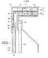
- FIG. 1Ais a perspective view of an example of a conventional liquid crystal display device, illustrating a positional relation between a liquid crystal display panel, a horizontal drive circuit substrate and a signal processing substrate thereof and FIG. 1B is a plan view of the signal processing substrate and a connecting unit for connecting the horizontal liquid crystal display panel to the signal processing substrate, which are extended in a plane.
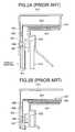
- FIG. 2 A and FIG. 2Bare cross sections taken along a line A—A′ in FIG. 1A, illustrating a portion of a second shield plate, which has no nail portion for fixing the connecting substrate to the second shield plate and a portion thereof, which has a nail portion provided appropriately, respectively.
- FIG. 3is a cross section taken along a line B—B′ in FIG. 1 A.
- the conventional liquid crystal display device 510is constructed with the liquid crystal display panel 511 , a front shield plate 531 , a first rear shield plate 533 , a second rear shield plate 534 , the signal processing substrate 521 , the horizontal drive circuit substrate 524 in the form of a TCP (Tape Carrier Package) on which horizontal driving IC's 526 are mounted, the connecting substrate 523 , a flexible printed circuit substrate (referred to as FPC, hereinafter) 522 and a light diffusing plate 513 for uniformly dispersing light from the backlight (not shown), etc.
- TCPTransmission Carrier Package
- FPCflexible printed circuit substrate
- the horizontal drive circuit substrate 524will be referred to as TCP, hereinafter.
- a peripheral portion of the display panel 511which is a non-display region, is sandwiched between the front shield plate 531 and the second rear shield plate 534 by way of a first spacer 546 and a second spacer plate 547 , respectively.
- the light diffusing plate 513 received and held by the first rear shield plate 533 and the backlight (not shown)are provided on the side of a rear surface (opposite to a display surface) of the liquid crystal display panel 511 .
- the signal processing substrate 521is fixed to a rear surface side of the first rear shield plate 533 via an insulating sheet 555 and the connecting substrate 523 is fixed to the second rear shield plate 534 in a plane substantially perpendicular to the display surface of the liquid crystal display panel 511 via the insulating sheet 551 .
- This fixation of the connecting substrate 523is performed by at least one nail portion 537 provided in an appropriate portion of the second rear shield plate 534 , as shown in FIG. 2 B.
- the portion of the second rear shield plate 534 in which the nail portion 537 is providedcorresponds to a region of the connecting substrate 523 in which any wiring pattern is not formed.
- a connecting unit 520 for connecting the signal processing substrate 521 to the liquid crystal display panel 511includes the FPC 522 , the connecting substrate 523 and the TCP 524 , as shown in FIG. 1 B.
- One end of the TCP 524(on the output end side) is bonded to electrodes provided in an edge portion of the liquid crystal display panel 511 by thermocompression bonding with using, for example, a thermoplastic, anisotropic electrically conductive film and the other end (input end side) thereof is connected to the connecting substrate 523 by, for example, soldering.
- the connecting substrate 523 and the signal processing substrate 521are connected to each other by the FPC 522 .
- an outer casing(not shown) having at least an electrically conductive inner surface portion and covering the whole rear surface of the liquid crystal display panel including the signal processing substrate 521 is provided on the rear surface side of the liquid crystal display device 510 .
- the front shield plate, the first rear shield plate and the second rear shield plateare connected to the inner surface portion of the outer casing.
- an electromagnetic shield structure for restricting EMI, etc., due to unnecessary electromagnetic radiation from electronic parts and wiring mounted on the signal processing substrate 521 , the TCP 524 and/or the vertical driving circuit substrate, which is not shown, etc.,is formed by connecting at least the electrically conductive inner surface portion of the outer casing covering these components to a common ground terminal (not shown) of the liquid crystal display device 510 .
- An object of the present inventionis to provide a display device such as a color liquid crystal display device having a structure with which unnecessary electromagnetic radiation, which may cause EMI, etc., can be restricted even when a number of high frequency signals are transmitted through a long wiring in a connecting substrate having limited wiring space.
- the display deviceis featured by comprising at least a display unit for displaying an image on a front surface of the display unit, a signal processing unit for processing an externally supplied image signal and outputting a first signal for displaying the image, a drive unit for receiving the first signal and outputting a second signal for driving the display unit, a connecting unit for connecting the signal processing unit to the display unit, a first shield unit formed of an electrically conductive material such as metal and having an opening portion corresponding to an image displaying region of the display unit, for electromagnetically shielding a peripheral region and a side face region of the image display surface and a second shield unit formed of an electrically conductive material such as metal, etc., for electromagnetically shielding a whole rear side surface of the display unit.
- the connecting unitcomprises a first flexible connecting portion connected to the signal processing unit, a second flexible connecting portion connected to the display unit and mounting the drive unit thereon and a connecting substrate for connecting the first flexible connecting portion and the second flexible connecting portion to each other, the connecting substrate being kept in a position between the first shield unit and the second shield unit separated from the first and second shield units by predetermined distances, respectively.
- the display devicemay further comprise a first support member for supporting a portion between the connecting substrate and the first shield unit and a second support member for supporting a portion between the connecting substrate and the second shield unit. Heights of the first and second support members are equal to each other.
- the first support member and the second support memberare preferably formed of electrically non-conductive material such as silicon rubber.
- the display unitmay be a liquid crystal display panel composed of two substrates opposing to each other with a predetermined gap therebetween and liquid crystal material layer arranged between the two substrates.
- FIG. 1Ais a perspective view of an example of a conventional liquid crystal display device, illustrating a positional relation between a liquid crystal display panel, a horizontal driving circuit substrate and a signal processing substrate thereof;
- FIG. 1Bis a plan view of the signal processing substrate and a connecting unit for connecting the horizontal liquid crystal display panel to the signal processing substrate, which are extended in a pane;
- FIG. 2Ais a detailed cross sections taken along a line A—A′ in FIG. 1A, illustrating a portion having no nail portion for fixing the connecting substrate to a second shield plate;
- FIG. 2Bis a detailed cross sections taken along a line A—A′ in FIG. 1A, illustrating a portion having at least one nail portion provided appropriately;
- FIG. 3is a cross section taken along a line B—B′ in FIG. 1A;
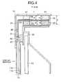
- FIG. 4is a cross section, illustrating a main portion of a liquid crystal display device according to an embodiment of the present invention
- FIG. 5is a cross section, illustrating a main portion of a liquid crystal display device according to an embodiment of the present invention.
- FIG. 6Ais a plan view showing a first example of a support member employed by the present invention.
- FIG. 6Bis a plan view showing a second example of the support member employed by the present invention.
- FIG. 6Cis a cross section taken along a line X 1 —X 1 ′ in FIG. 6B;
- FIG. 6Dis a cross section taken along a line Y 1 —Y 1 ′ in FIG. 6A;
- FIG. 6Eis a cross section taken along a line Y 2 —Y 2 ′ in FIG. 6B;
- FIG. 6Fis a plan view showing a third example of the support member employed by the present invention.
- FIG. 6Gis a plan view showing a fourth example of the support member employed by the present invention.
- FIG. 6His a cross section taken along a line X 2 —X 2 ′ in FIG. 6 F and FIG. 6G;
- FIG. 6Iis a cross section taken along a line Y 3 —Y 3 ′ in FIG. 6F;
- FIG. 6Jis a cross section taken along a line Y 4 —Y 4 ′ in FIG. 6G;
- FIG. 7is a graph showing an example of a result of measurement of unnecessary electromagnetic radiation from the liquid crystal display device according to the embodiment of the present invention.
- FIG. 8is a block diagram of an electromagnetic radiation measuring system with which unnecessary electromagnetic radiation of the display device is measured.
- FIG. 4 and FIG. 5are cross sections showing main portions of a liquid crystal display device according to an embodiment of the present invention, respectively.
- a positional relation between a liquid crystal display panel, a horizontal driving circuit substrate and a signal processing substrate in the liquid crystal display device of this embodimentis similar to that in the conventional liquid crystal display device shown in FIG. 1 and FIG. 4 and FIG. 5 are cross sections taken along the lines A—A′ and B—B′ in FIG. 1A, respectively.
- the liquid crystal display device 10 of the embodimentis constructed with at least a liquid crystal display panel 11 as a display unit for displaying an image on a front surface side, a signal processing substrate 21 as a signal processing unit for processing an externally supplied image signal and outputting a first signal for displaying the image, driving IC's 26 as a driving unit responsive to the first signal from the signal processing substrate 21 for outputting a second signal for driving the liquid crystal display panel 11 , a front shield plate 31 as a first metal shield unit having an opening portion in an image display region of the liquid crystal display panel 11 , for electromagnetically shielding a peripheral region and a side face region of an image display surface side of the liquid crystal display panel 11 , a first rear shield plate 33 and a second rear shield plate 34 as a metal second shield unit for covering the whole rear surface side of the liquid crystal display panel 11 , an FPC 22 as a first flexible connecting portion for connecting the signal processing substrate 22 , a TCP 24 as a connecting substrate for
- the first rear shield plate 33 and the second rear shield plate 34are mutually connected by, for example, screws (not shown).
- the connecting unit 20 for connecting the liquid crystal display panel 11 and the signal processing plate 21includes the FPC 22 , the connecting substrate 23 and the TCP 24 .
- the peripheral portion of the liquid crystal display panel 11 of the liquid crystal display device 10 of the present inventionis sandwiched between the front shield plate 31 and the second rear shield plate 34 with a first spacer 46 and a second spacer 47 inside them, respectively.
- a light diffusing plate 13 received and held by the first rear shield plate 33 and a backlight, which is not shown,are provided on the side of a rear surface (opposite to a display surface) of the liquid crystal display panel 11 .
- the signal processing substrate 21is fixed to a rear surface side of the first rear shield plate 33 through, for example, an insulating sheet 55 and the connecting substrate 23 is supported between the front shield plate 31 and the second rear shield plate 34 through the first support members 41 and the second support members 43 and fixed therein in a plane substantially perpendicular to the display surface of the liquid crystal display panel 11 .
- the first support members 41 and the second support members 43may be formed of an electrically non-conductive material such as, for example, silicon rubber.
- the position of the connecting substrate 23 in vertical directionis defined in such a way that, representing the distance between the opposing surfaces of the front shield plate 31 and the second rear shield plate 34 by L and distances between a center line 28 of the connecting substrate 23 in a thickness direction thereof and the surfaces of the front shield plate 31 and the second rear shield plate 33 , which oppose to the connecting substrate 23 , by d 1 and d 2 , respectively, d 1 and d 2 satisfy the following relations to L:
- d 1 and d 2may be equal, for example.
- the liquid crystal display panel 11includes a glass substrate 11 a on which a plurality of transistors, for example, are formed in matrix, an opposing substrate 11 b having an opposing electrode and a liquid crystal material layer (not shown) sandwiched between these substrates arranged in parallel with a predetermined gap therebetween.
- One end (output side) of the TCP 24is bonded to the electrodes provided on side face portion of the glass substrate 11 a of the liquid crystal display panel 11 by thermocompression bonding with using, for example, electrically conductive anisotropic film of thermoplastic material and the other end (input end side) thereof is bonded to the connecting substrate 23 by thermocompression bonding.
- the connecting substrate 23 and the signal processing substrate 521are connected to each other by the FPC 22 .
- the liquid crystal display device 10 of this embodimentincludes an outer casing (not shown), which is provided on the side of the rear surface.
- the outer casinghas at least inner side thereof, which is electrically conductive, and covers the whole portion of the device including the signal processing substrate 21 .
- the outer casingis fixed to the first rear shield plate 33 and the second rear shield 34 by, for example, screws. Incidentally, it may be possible on demand to electrically connect the outer casing, the first rear shield plate 33 and the second rear shield plate 34 together by such as metal leaf springs (fingers) to reinforce the electric connection thereof.
- the connecting substrate 23is separated from the front shield plate 31 as well as the second rear shield plate 34 , a capacitive coupling between the wiring on the connecting substrate 23 and the first shield plate 31 and the second rear shield plate 34 becomes small enough. Therefore, leakage of high frequency signal to the front shield plate 31 and the second rear shield plate 34 becomes sufficiently small even when a number of high frequency signals are transmitted through a long wiring on the connecting substrate 23 having limited wiring space. Thus, unnecessary electromagnetic radiation caused by the front shield plate 31 and the second rear shield plate 34 , which function an antenna can be restricted.
- FIG. 6A to FIG. 6Jshow various examples of configurations of the support members.
- FIG. 6A, FIG. 6B, FIG. 6 F and FIG. 6Gare plan views showing four examples of a pattern of the configuration of the support member when the connecting substrate 23 is looked from a P portion side in FIG. 4 or FIG. 1 (in order to facilitate the understanding, the front shield plate 31 is removed).
- FIG. 6C, FIG. 6D, FIG. 6E, FIG. 6H, FIG. 6 I and FIG. 6Jare cross sections thereof illustrating the supporting state of the first support member 41 and the second support member 43 supporting the connecting substrate 23 .
- each of the first support member 41 and the second support member 43is constructed with two support pieces for supporting substantially a whole length of a longer side of the connecting substrate 23 and, in the example shown in FIG. 6B, constructed with a single support piece for supporting a whole area of the connecting substrate 23 .
- the two support pieces shown in FIG. 6 A and the single support piece shown in FIG. 6Bare divided to a plurality of supporting pieces in the longer side direction of the connecting substrate 23 to thin them with opposite end portions thereof in the longer side direction being left as they are.
- FIG. 7is a graph showing a result of measurement of unnecessary electromagnetic radiation from the liquid crystal display device of this embodiment
- FIG. 8is a block diagram of a measuring system for measuring unnecessary electromagnetic radiation.
- the liquid crystal display device 10such as shown in FIG. 4, which has the outer casing, is mounted on a turntable 73 within a predetermined shield room 70 .
- An antenna 71 for measuring an amount of electromagnetic radiation from the liquid crystal display device 10is arranged in the shield room 70 at a position remote from the measuring object, that is, the liquid crystal display device 10 , on the turntable by 3 m.
- the measuring objectis positioned in a center of the turntable 73 .
- the antenna 71is connected to an EMI receiver 76 arranged outside the shield room 70 .
- Positions of the antenna 71 and the turntable 73are controlled by a controller 77 arranged outside the shield room 70 such that a distance between the liquid crystal display device 10 as the measuring object and the antenna 71 becomes 3 m. Further, the EMI receiver 76 and the controller 77 are connected to a control PC 75 arranged outside the shield room 70 , for controlling the whole measuring system.
- the measurementis performed by using this measuring system. That is, a power source of the liquid crystal display device 10 is turned off and a power source for the PC 61 , the keyboard 62 and the mouse 63 is turned on to make the system in a usual operating state. In this state, an amount of electromagnetic radiation is measured. And then, a power source of the liquid crystal display device 10 is turned on and an amount of electromagnetic radiation is measured. A difference in amount of electromagnetic radiation between the first measurement and the second measurement is the amount of electromagnetic radiation from the liquid crystal display device 10 . This measurement is performed for a predetermined frequency range.
- FIG. 7is a graph showing a result of the measurement performed by changing a distance d 2 between the connecting substrate 23 and the second rear shield plate 34 of the liquid crystal display device 10 and changing a frequency in a range from 30 MHz to 1000 MHz for every value of d 2 .
- Ordinateindicates the amount of electromagnetic radiation (noise level) of the liquid crystal display device 10 by peak values of electromagnetic radiation and abscissa indicates the distance d 2 between the second rear shield plate 34 and the centerline 28 of the connecting substrate 23 .
- d 2is shown as a ratio to the distance L between the front shield plate 31 and the second rear shield plate 34 .
- the peak noise levelis obtained at frequency of 208 MHz (vertical polarized electromagnetic radiation).
- the present inventionis not limited thereto. It is possible to obtain similar effect to that described above in a display device such as a flat type display device such as, for example, an EL display device, etc., which has a construction in which high frequency signal is transmitted through a long transmission line on a connecting substrate having a limited wiring space.
- a display devicesuch as a flat type display device such as, for example, an EL display device, etc., which has a construction in which high frequency signal is transmitted through a long transmission line on a connecting substrate having a limited wiring space.
- the display device according to the present inventionhas a merit that it is possible to restrict EMI, etc., of a display device since it is possible to restrict unnecessary electromagnetic radiation from the connecting substrate even when high frequency signal is transmitted through a long transmission line on a connecting substrate having a limited wiring space.
Landscapes
- Physics & Mathematics (AREA)
- Nonlinear Science (AREA)
- Mathematical Physics (AREA)
- Chemical & Material Sciences (AREA)
- Crystallography & Structural Chemistry (AREA)
- General Physics & Mathematics (AREA)
- Optics & Photonics (AREA)
- Liquid Crystal (AREA)
- Devices For Indicating Variable Information By Combining Individual Elements (AREA)
- Shielding Devices Or Components To Electric Or Magnetic Fields (AREA)
Abstract
Description
1. Field of the Invention
The present invention relates to a flat panel type display device of such as a color liquid crystal display device and, in particular, the present invention relates to a flat panel type display device constructed such that unnecessary electromagnetic radiation, which may bring about EMI (Electro-magnetic Interference), etc., is restricted.
2. Description of the Prior Art
As a flat panel type display device, a color liquid crystal display device of an active matrix system, for example, includes a liquid crystal display panel and a backlight for illuminating a lower surface of the liquid crystal display panel. A horizontal drive circuit substrate and a vertical drive circuit substrate are arranged outside an outer peripheral portion of the liquid crystal display panel. Further, a signal processing substrate for converting an externally supplied image signal into a horizontal drive signal and supplying the latter signal to a liquid crystal driving IC on the horizontal drive circuit substrate by way of a connecting substrate is arranged on a rear surface side of the liquid crystal display panel. The liquid crystal display panel, the backlight and the horizontal and vertical drive circuit substrates are accommodated in a casing constructed with a front shield plate, which is formed of a metal and has a display window, and a metal rear shield plate for accommodating and holding the backlight.
FIG. 1A is a perspective view of an example of a conventional liquid crystal display device, illustrating a positional relation between a liquid crystal display panel, a horizontal drive circuit substrate and a signal processing substrate thereof and FIG. 1B is a plan view of the signal processing substrate and a connecting unit for connecting the horizontal liquid crystal display panel to the signal processing substrate, which are extended in a plane. Further, FIG.2A and FIG. 2B are cross sections taken along a line A—A′ in FIG. 1A, illustrating a portion of a second shield plate, which has no nail portion for fixing the connecting substrate to the second shield plate and a portion thereof, which has a nail portion provided appropriately, respectively. Incidentally, in order to simplify the illustration, the vertical drive circuit substrate, the front shield plate, the rear shield plate and the backlight, etc, are not shown in FIG.1A. FIG. 3 is a cross section taken along a line B—B′ in FIG.1A.
Referring to FIG. 1A to FIG. 3, the conventional liquidcrystal display device 510 is constructed with the liquidcrystal display panel 511, afront shield plate 531, a firstrear shield plate 533, a secondrear shield plate 534, thesignal processing substrate 521, the horizontaldrive circuit substrate 524 in the form of a TCP (Tape Carrier Package) on which horizontal driving IC's526 are mounted, the connectingsubstrate 523, a flexible printed circuit substrate (referred to as FPC, hereinafter)522 and alight diffusing plate 513 for uniformly dispersing light from the backlight (not shown), etc. Incidentally, the horizontaldrive circuit substrate 524 will be referred to as TCP, hereinafter.
A peripheral portion of thedisplay panel 511, which is a non-display region, is sandwiched between thefront shield plate 531 and the secondrear shield plate 534 by way of afirst spacer 546 and asecond spacer plate 547, respectively. The light diffusingplate 513 received and held by the firstrear shield plate 533 and the backlight (not shown) are provided on the side of a rear surface (opposite to a display surface) of the liquidcrystal display panel 511.
As shown in FIG. 3, thesignal processing substrate 521 is fixed to a rear surface side of the firstrear shield plate 533 via aninsulating sheet 555 and the connectingsubstrate 523 is fixed to the secondrear shield plate 534 in a plane substantially perpendicular to the display surface of the liquidcrystal display panel 511 via theinsulating sheet 551. This fixation of the connectingsubstrate 523 is performed by at least onenail portion 537 provided in an appropriate portion of the secondrear shield plate 534, as shown in FIG.2B. The portion of the secondrear shield plate 534 in which thenail portion 537 is provided corresponds to a region of the connectingsubstrate 523 in which any wiring pattern is not formed. Incidentally, a connectingunit 520 for connecting thesignal processing substrate 521 to the liquidcrystal display panel 511 includes the FPC522, the connectingsubstrate 523 and the TCP524, as shown in FIG.1B.
One end of the TCP524 (on the output end side) is bonded to electrodes provided in an edge portion of the liquidcrystal display panel 511 by thermocompression bonding with using, for example, a thermoplastic, anisotropic electrically conductive film and the other end (input end side) thereof is connected to the connectingsubstrate 523 by, for example, soldering. The connectingsubstrate 523 and thesignal processing substrate 521 are connected to each other by the FPC522.
Incidentally, an outer casing (not shown) having at least an electrically conductive inner surface portion and covering the whole rear surface of the liquid crystal display panel including thesignal processing substrate 521 is provided on the rear surface side of the liquidcrystal display device 510. The front shield plate, the first rear shield plate and the second rear shield plate are connected to the inner surface portion of the outer casing.
In the conventional liquidcrystal display device 510 described above, an electromagnetic shield structure for restricting EMI, etc., due to unnecessary electromagnetic radiation from electronic parts and wiring mounted on thesignal processing substrate 521, the TCP524 and/or the vertical driving circuit substrate, which is not shown, etc., is formed by connecting at least the electrically conductive inner surface portion of the outer casing covering these components to a common ground terminal (not shown) of the liquidcrystal display device 510.
However, with the recent tendency of increase of the operating frequency, particularly, the horizontal driving frequency, of the liquid crystal display device, unnecessary electromagnetic radiation becomes a problem in, particularly, the connectingsubstrate 523 in which a number of horizontal drive signals are transmitted along a long wiring within a limited region. As shown in FIG. 2A, FIG.2B and FIG. 3, the connectingsubstrate 523 is fixed to the secondrear shield pate 534 via thethin insulating sheet 551 and, therefore, the electric insulation is maintained. However, it has been found that, when a number of high frequency signals flow in the connectingsubstrate 523, the signals are leaked between the firstrear shield plate 533 and the secondrear shield plate 534 by such as capacitive coupling and unnecessary electromagnetic radiation occurs through the firstrear shield plate 533 and the secondrear shield plate 534 as an antenna.
An object of the present invention is to provide a display device such as a color liquid crystal display device having a structure with which unnecessary electromagnetic radiation, which may cause EMI, etc., can be restricted even when a number of high frequency signals are transmitted through a long wiring in a connecting substrate having limited wiring space.
In order to achieve the above object, the display device according to the present invention is featured by comprising at least a display unit for displaying an image on a front surface of the display unit, a signal processing unit for processing an externally supplied image signal and outputting a first signal for displaying the image, a drive unit for receiving the first signal and outputting a second signal for driving the display unit, a connecting unit for connecting the signal processing unit to the display unit, a first shield unit formed of an electrically conductive material such as metal and having an opening portion corresponding to an image displaying region of the display unit, for electromagnetically shielding a peripheral region and a side face region of the image display surface and a second shield unit formed of an electrically conductive material such as metal, etc., for electromagnetically shielding a whole rear side surface of the display unit. The connecting unit comprises a first flexible connecting portion connected to the signal processing unit, a second flexible connecting portion connected to the display unit and mounting the drive unit thereon and a connecting substrate for connecting the first flexible connecting portion and the second flexible connecting portion to each other, the connecting substrate being kept in a position between the first shield unit and the second shield unit separated from the first and second shield units by predetermined distances, respectively.
It is referable that, representing the distance between the first shield unit and the second shield unit arranged on the connecting substrate by L and distances between a center of the connecting substrate in thickness direction and the first shield unit and the second shield unit by d1 and d2, respectively, d1 and d2 satisfy the following relations to L:
The display device may further comprise a first support member for supporting a portion between the connecting substrate and the first shield unit and a second support member for supporting a portion between the connecting substrate and the second shield unit. Heights of the first and second support members are equal to each other. The first support member and the second support member are preferably formed of electrically non-conductive material such as silicon rubber.
The display unit may be a liquid crystal display panel composed of two substrates opposing to each other with a predetermined gap therebetween and liquid crystal material layer arranged between the two substrates.
FIG. 1A is a perspective view of an example of a conventional liquid crystal display device, illustrating a positional relation between a liquid crystal display panel, a horizontal driving circuit substrate and a signal processing substrate thereof;
FIG. 1B is a plan view of the signal processing substrate and a connecting unit for connecting the horizontal liquid crystal display panel to the signal processing substrate, which are extended in a pane;
FIG. 2A is a detailed cross sections taken along a line A—A′ in FIG. 1A, illustrating a portion having no nail portion for fixing the connecting substrate to a second shield plate;
FIG. 2B is a detailed cross sections taken along a line A—A′ in FIG. 1A, illustrating a portion having at least one nail portion provided appropriately;
FIG. 3 is a cross section taken along a line B—B′ in FIG. 1A;
FIG. 4 is a cross section, illustrating a main portion of a liquid crystal display device according to an embodiment of the present invention;
FIG. 5 is a cross section, illustrating a main portion of a liquid crystal display device according to an embodiment of the present invention;
FIG. 6A is a plan view showing a first example of a support member employed by the present invention;
FIG. 6B is a plan view showing a second example of the support member employed by the present invention;
FIG. 6C is a cross section taken along a line X1—X1′ in FIG. 6B;
FIG. 6D is a cross section taken along a line Y1—Y1′ in FIG. 6A;
FIG. 6E is a cross section taken along a line Y2—Y2′ in FIG. 6B;
FIG. 6F is a plan view showing a third example of the support member employed by the present invention;
FIG. 6G is a plan view showing a fourth example of the support member employed by the present invention;
FIG. 6H is a cross section taken along a line X2—X2′ in FIG.6F and FIG. 6G;
FIG. 6I is a cross section taken along a line Y3—Y3′ in FIG. 6F;
FIG. 6J is a cross section taken along a line Y4—Y4′ in FIG. 6G;
FIG. 7 is a graph showing an example of a result of measurement of unnecessary electromagnetic radiation from the liquid crystal display device according to the embodiment of the present invention; and
FIG. 8 is a block diagram of an electromagnetic radiation measuring system with which unnecessary electromagnetic radiation of the display device is measured.
The present invention will be described with reference to the drawings.
FIG.4 and FIG. 5 are cross sections showing main portions of a liquid crystal display device according to an embodiment of the present invention, respectively. Incidentally, a positional relation between a liquid crystal display panel, a horizontal driving circuit substrate and a signal processing substrate in the liquid crystal display device of this embodiment is similar to that in the conventional liquid crystal display device shown in FIG.1 and FIG.4 and FIG. 5 are cross sections taken along the lines A—A′ and B—B′ in FIG. 1A, respectively.
Referring to FIG.4 and FIG. 5 together with FIG. 1, the liquid crystal display device10 of the embodiment is constructed with at least a liquid crystal display panel11 as a display unit for displaying an image on a front surface side, a signal processing substrate21 as a signal processing unit for processing an externally supplied image signal and outputting a first signal for displaying the image, driving IC's26 as a driving unit responsive to the first signal from the signal processing substrate21 for outputting a second signal for driving the liquid crystal display panel11, a front shield plate31 as a first metal shield unit having an opening portion in an image display region of the liquid crystal display panel11, for electromagnetically shielding a peripheral region and a side face region of an image display surface side of the liquid crystal display panel11, a first rear shield plate33 and a second rear shield plate34 as a metal second shield unit for covering the whole rear surface side of the liquid crystal display panel11, an FPC22 as a first flexible connecting portion for connecting the signal processing substrate22, a TCP24 as a connecting substrate for connecting the FPC22 and the TCP24, a first support member41 and a second support member43 for supporting portions between the connecting substrate23 and the front shield plate31 and between the connecting porting substrate23 and the second rear shield plate34, respectively, a backlight, which is not shown, and a light diffusing plate13 for uniformly dispersing light from the backlight. Incidentally, the firstrear shield plate 33 and the secondrear shield plate 34 are mutually connected by, for example, screws (not shown). Further, the connectingunit 20 for connecting the liquidcrystal display panel 11 and thesignal processing plate 21 includes theFPC 22, the connectingsubstrate 23 and theTCP 24.
Similarly to the conventional liquid crystal display device, the peripheral portion of the liquidcrystal display panel 11 of the liquidcrystal display device 10 of the present invention is sandwiched between thefront shield plate 31 and the secondrear shield plate 34 with afirst spacer 46 and asecond spacer 47 inside them, respectively. Alight diffusing plate 13 received and held by the firstrear shield plate 33 and a backlight, which is not shown, are provided on the side of a rear surface (opposite to a display surface) of the liquidcrystal display panel 11. Thesignal processing substrate 21 is fixed to a rear surface side of the firstrear shield plate 33 through, for example, an insulatingsheet 55 and the connectingsubstrate 23 is supported between thefront shield plate 31 and the secondrear shield plate 34 through thefirst support members 41 and thesecond support members 43 and fixed therein in a plane substantially perpendicular to the display surface of the liquidcrystal display panel 11. Thefirst support members 41 and thesecond support members 43 may be formed of an electrically non-conductive material such as, for example, silicon rubber. The position of the connectingsubstrate 23 in vertical direction is defined in such a way that, representing the distance between the opposing surfaces of thefront shield plate 31 and the secondrear shield plate 34 by L and distances between acenter line 28 of the connectingsubstrate 23 in a thickness direction thereof and the surfaces of thefront shield plate 31 and the secondrear shield plate 33, which oppose to the connectingsubstrate 23, by d1 and d2, respectively, d1 and d2 satisfy the following relations to L:
In a usual case, d1 and d2 may be equal, for example. Alternatively, representing heights of thefirst support member 41 and thesecond support member 43, that is, distances between the connectingsubstrate 23 and thefront shield plate 31 and between the connectingsubstrate 23 and thesecond shield substrate 34, by h1 and h2, respectively, h1 and h2 may be defined by h1=h2.
The liquidcrystal display panel 11 includes a glass substrate11aon which a plurality of transistors, for example, are formed in matrix, an opposingsubstrate 11bhaving an opposing electrode and a liquid crystal material layer (not shown) sandwiched between these substrates arranged in parallel with a predetermined gap therebetween. One end (output side) of theTCP 24 is bonded to the electrodes provided on side face portion of the glass substrate11aof the liquidcrystal display panel 11 by thermocompression bonding with using, for example, electrically conductive anisotropic film of thermoplastic material and the other end (input end side) thereof is bonded to the connectingsubstrate 23 by thermocompression bonding. The connectingsubstrate 23 and thesignal processing substrate 521 are connected to each other by theFPC 22.
The liquidcrystal display device 10 of this embodiment includes an outer casing (not shown), which is provided on the side of the rear surface. The outer casing has at least inner side thereof, which is electrically conductive, and covers the whole portion of the device including thesignal processing substrate 21. The outer casing is fixed to the firstrear shield plate 33 and the secondrear shield 34 by, for example, screws. Incidentally, it may be possible on demand to electrically connect the outer casing, the firstrear shield plate 33 and the secondrear shield plate 34 together by such as metal leaf springs (fingers) to reinforce the electric connection thereof. Further, since the connectingsubstrate 23 is separated from thefront shield plate 31 as well as the secondrear shield plate 34, a capacitive coupling between the wiring on the connectingsubstrate 23 and thefirst shield plate 31 and the secondrear shield plate 34 becomes small enough. Therefore, leakage of high frequency signal to thefront shield plate 31 and the secondrear shield plate 34 becomes sufficiently small even when a number of high frequency signals are transmitted through a long wiring on the connectingsubstrate 23 having limited wiring space. Thus, unnecessary electromagnetic radiation caused by thefront shield plate 31 and the secondrear shield plate 34, which function an antenna can be restricted.
Although configurations of thefirst support member 41 and thesecond support member 43 are not described in detail, the configurations thereof are not specifically limited provided that the distance between thefront shield plate 31 and the secondrear shield plate 34 can be maintained without warping the connectingsubstrate 23. FIG. 6A to FIG. 6J show various examples of configurations of the support members. In FIG. 6A, FIG. 6B, FIG.6F and FIG. 6G are plan views showing four examples of a pattern of the configuration of the support member when the connectingsubstrate 23 is looked from a P portion side in FIG. 4 or FIG. 1 (in order to facilitate the understanding, thefront shield plate 31 is removed). FIG. 6C, FIG. 6D, FIG. 6E, FIG. 6H, FIG.6I and FIG. 6J are cross sections thereof illustrating the supporting state of thefirst support member 41 and thesecond support member 43 supporting the connectingsubstrate 23.
In the example shown in FIG. 6A, each of thefirst support member 41 and thesecond support member 43 is constructed with two support pieces for supporting substantially a whole length of a longer side of the connectingsubstrate 23 and, in the example shown in FIG. 6B, constructed with a single support piece for supporting a whole area of the connectingsubstrate 23. In the examples shown in FIG.6F and FIG. 6G, the two support pieces shown in FIG.6A and the single support piece shown in FIG. 6B are divided to a plurality of supporting pieces in the longer side direction of the connectingsubstrate 23 to thin them with opposite end portions thereof in the longer side direction being left as they are.
The restricting effect of unnecessary electromagnetic radiation in the liquid crystal display device according to this embodiment will be described with reference to FIG.7 and FIG. 8 in which FIG. 7 is a graph showing a result of measurement of unnecessary electromagnetic radiation from the liquid crystal display device of this embodiment and FIG. 8 is a block diagram of a measuring system for measuring unnecessary electromagnetic radiation.
A construction of the measuring system shown in FIG. 8 will be described first. Together with a personal computer (referred to as PC, hereinafter)61, akeyboard 62 and amouse 63, etc., the liquidcrystal display device 10 such as shown in FIG. 4, which has the outer casing, is mounted on aturntable 73 within apredetermined shield room 70. Anantenna 71 for measuring an amount of electromagnetic radiation from the liquidcrystal display device 10 is arranged in theshield room 70 at a position remote from the measuring object, that is, the liquidcrystal display device 10, on the turntable by 3 m. Usually, the measuring object is positioned in a center of theturntable 73. Theantenna 71 is connected to anEMI receiver 76 arranged outside theshield room 70. Positions of theantenna 71 and theturntable 73 are controlled by acontroller 77 arranged outside theshield room 70 such that a distance between the liquidcrystal display device 10 as the measuring object and theantenna 71 becomes 3 m. Further, theEMI receiver 76 and thecontroller 77 are connected to acontrol PC 75 arranged outside theshield room 70, for controlling the whole measuring system.
The measurement is performed by using this measuring system. That is, a power source of the liquidcrystal display device 10 is turned off and a power source for thePC 61, thekeyboard 62 and themouse 63 is turned on to make the system in a usual operating state. In this state, an amount of electromagnetic radiation is measured. And then, a power source of the liquidcrystal display device 10 is turned on and an amount of electromagnetic radiation is measured. A difference in amount of electromagnetic radiation between the first measurement and the second measurement is the amount of electromagnetic radiation from the liquidcrystal display device 10. This measurement is performed for a predetermined frequency range. Further, it is possible to measure an amount of electromagnetic radiation in a periphery of the liquidcrystal display device 10 by performing the measurement while changing height of theantenna 71 within a predetermined range (for example, in a range from 1 m to 2 m) and successively changing an angle of the liquidcrystal display device 10 with respect to theantenna 71 by rotating theturntable 73. FIG. 7 is a graph showing a result of the measurement performed by changing a distance d2 between the connectingsubstrate 23 and the secondrear shield plate 34 of the liquidcrystal display device 10 and changing a frequency in a range from 30 MHz to 1000 MHz for every value of d2. Ordinate indicates the amount of electromagnetic radiation (noise level) of the liquidcrystal display device 10 by peak values of electromagnetic radiation and abscissa indicates the distance d2 between the secondrear shield plate 34 and thecenterline 28 of the connectingsubstrate 23. Incidentally, in this graph, d2 is shown as a ratio to the distance L between thefront shield plate 31 and the secondrear shield plate 34. In this example, the peak noise level is obtained at frequency of 208 MHz (vertical polarized electromagnetic radiation). Referring to FIG. 7, the noise level, that is, the peak value of unnecessary electromagnetic radiation in the frequency range from 30 MHz to 1000 MHz, becomes minimum in the distance range d2=(3/7)L to L/2.
Although the embodiment has been described by using the liquid crystal display device as an example, the present invention is not limited thereto. It is possible to obtain similar effect to that described above in a display device such as a flat type display device such as, for example, an EL display device, etc., which has a construction in which high frequency signal is transmitted through a long transmission line on a connecting substrate having a limited wiring space.
As described hereinbefore, the display device according to the present invention has a merit that it is possible to restrict EMI, etc., of a display device since it is possible to restrict unnecessary electromagnetic radiation from the connecting substrate even when high frequency signal is transmitted through a long transmission line on a connecting substrate having a limited wiring space.
Claims (6)
1. A display device comprising:
a display unit for displaying an image on a front surface thereof;
a signal processing unit for outputting a first signal for image display by processing an externally supplied image signal:
a drive unit responsive the first signal from said signal processing unit or outputting a second signal for driving said display unit;
a connecting unit for connecting said signal processing unit and said display unit, said connecting unit comprising a first flexible connecting portion connected to said signal processing unit, a second flexible connecting portion connected to said display unit and mounting said drive unit thereon and a connecting substrate portion for connecting said first flexible connecting portion and said second flexible connecting portion;
an electrically conductive first shield unit having an opening portion in an image display region of said display unit and electromagnetically shielding a peripheral region and a side surface region of said image display region;
an electrically conductive second shield unit for electromagneticall shielding a whole rear surface side of said display unit and supporting said connecting substrate portion in a position between said first shield unit and said second shield unit, with said connecting substrate portion remote from said second shield unit and remote from said first shield unit by predetermined distances, respectively; and
wherein, representing the distance between said first shield unit and said second shield unit by L and distances between a center of said connecting substrate portion in a thickness direction thereof and said first shield unit and said second shield unit by d1 and d2, respectively, d1 and d2 satisfy the following relations to L:
2. A display device as claimed inclaim 1 , wherein said display unit is a liquid crystal display panel including two substrates arranged in parallel with a predetermined gap and liquid crystal material layer sandwiched between said two substrates.
3. A display device comprising:
a display unit for displaying an image on a front surface thereof;
a signal processing unit for outputting a first signal for image display by processing an externally supplied image signal;
a drive unit responsive the first signal from said signal processing unit or outputting a second signal for driving said display unit;
a connecting unit for connecting said signal processing unit and said play unit, said connecting unit comprising a first flexible connecting portion connected to said signal processing unit, a second flexible connecting portion connected to said display unit and mounting said drive unit thereon and a connecting substrate portion for connecting said first flexible connecting portion and said second flexible connecting portion;
an electrically conductive first shield unit having an opening portion in an image display region of said display unit and electromagnetically shielding a peripheral region and a side surface region of said image display region;
an electrically conductive second shield unit for electromagneticall shielding a whole rear surface side of said display unit and supporting said connecting substrate portion in a position between said first shield unit and said second shield unit, with said connecting substrate portion remote from said first shield unit and said second shield unit by predetermined distances, respectively; and
a first support member for supporting an area between said connecting substrate portion and said first shield unit and a second support member for supporting an area between said connecting substrate portion and said second shield unit, wherein heights of said first and second support members corresponding to respective distances between said connecting substrate portion and said first and second shield units are equal to each other.
4. A display device as claimed inclaim 3 , wherein said first support member and said second support member are formed of electrically non-conductive material.
5. A display device as claimed inclaim 4 , wherein said electrically non-conductive material is silicon rubber.
6. A display device as claimed inclaim 3 , wherein said display unit is a liquid crystal display panel including two substrates arranged in parallel with a predetermined gap and liquid crystal material layer sandwiched between said two substrates.
Applications Claiming Priority (3)
| Application Number | Priority Date | Filing Date | Title |
|---|---|---|---|
| JP63255/2001 | 2001-03-07 | ||
| JP2001063255AJP4708587B2 (en) | 2001-03-07 | 2001-03-07 | Display device |
| JP2001-063255 | 2001-03-07 |
Publications (2)
| Publication Number | Publication Date |
|---|---|
| US20020126248A1 US20020126248A1 (en) | 2002-09-12 |
| US6801195B2true US6801195B2 (en) | 2004-10-05 |
Family
ID=18922279
Family Applications (1)
| Application Number | Title | Priority Date | Filing Date |
|---|---|---|---|
| US10/091,895Expired - LifetimeUS6801195B2 (en) | 2001-03-07 | 2002-03-06 | Display device |
Country Status (2)
| Country | Link |
|---|---|
| US (1) | US6801195B2 (en) |
| JP (1) | JP4708587B2 (en) |
Cited By (13)
| Publication number | Priority date | Publication date | Assignee | Title |
|---|---|---|---|---|
| US20050117283A1 (en)* | 2003-08-04 | 2005-06-02 | Samsung Electronics Co., Ltd. | Display apparatus and method |
| US20060187644A1 (en)* | 2005-02-24 | 2006-08-24 | Woo-Man Jeong | Plasma display device |
| US7295258B2 (en)* | 2003-09-10 | 2007-11-13 | Sharp Kabushiki Kaisha | Display device and liquid crystal display device having a back frame configuration that increases torsional strength |
| US20080297999A1 (en)* | 2007-06-04 | 2008-12-04 | Choi Man Yong | Display apparatus |
| US20080298001A1 (en)* | 2007-06-04 | 2008-12-04 | Choi Man Yong | Display apparatus |
| US20090086420A1 (en)* | 2007-10-01 | 2009-04-02 | General Dynamics Itronix Corporation | Rugged conductive housing structure for portable computing device display |
| US20090122238A1 (en)* | 2007-11-13 | 2009-05-14 | Samsung Corning Precision Glass Co., Ltd. | Protection Filter For Liquid Crystal Display |
| US20090141198A1 (en)* | 2007-12-03 | 2009-06-04 | Jin Hyuk Kim | Display apparatus |
| US20090210922A1 (en)* | 2008-02-19 | 2009-08-20 | At&T Knowledge Ventures, L.P. | System for configuring soft keys in a media communication system |
| US20100046193A1 (en)* | 2007-06-04 | 2010-02-25 | Lg Electronics, Inc. | Display apparatus |
| US7760491B2 (en) | 2007-06-04 | 2010-07-20 | Lg Electronics Inc. | Display apparatus |
| US20120268686A1 (en)* | 2011-04-21 | 2012-10-25 | Lg Display Co., Ltd. | Liquid Crystal Display Device |
| US9417473B2 (en) | 2012-02-06 | 2016-08-16 | Sharp Kabushiki Kaisha | Display device with a frame holding a drive board and television device having the display device |
Families Citing this family (84)
| Publication number | Priority date | Publication date | Assignee | Title |
|---|---|---|---|---|
| KR100913307B1 (en)* | 2002-12-12 | 2009-08-26 | 삼성전자주식회사 | Backlight assembly and liquid crystal display having the same |
| JP2005107498A (en) | 2003-09-10 | 2005-04-21 | Sharp Corp | Surface light source device and liquid crystal display device |
| US7495714B2 (en)* | 2003-10-07 | 2009-02-24 | American Panel Corporation | Flat panel display having an isolated EMI layer and integral heater and thermal sensors |
| US7265809B2 (en)* | 2003-10-07 | 2007-09-04 | Universal Avionics Systems Corporation | Flat panel display having integral metal heater optically hidden behind an EMI shield |
| KR101191163B1 (en)* | 2003-10-23 | 2012-10-15 | 엘지디스플레이 주식회사 | Liquid crystal display device module |
| KR100627384B1 (en)* | 2003-11-11 | 2006-09-21 | 삼성에스디아이 주식회사 | Plasma display device with driver IC heat dissipation structure |
| KR100553759B1 (en) | 2004-04-29 | 2006-02-20 | 삼성에스디아이 주식회사 | Plasma display |
| JP4774709B2 (en)* | 2004-09-30 | 2011-09-14 | ソニー株式会社 | Liquid crystal display |
| US8009262B2 (en)* | 2005-02-14 | 2011-08-30 | American Panel Corporation | Flat panel display wtih external integral heater |
| KR100749473B1 (en)* | 2005-03-14 | 2007-08-14 | 삼성에스디아이 주식회사 | Plasma display device |
| CN100443975C (en)* | 2005-12-21 | 2008-12-17 | 群康科技(深圳)有限公司 | Liquid crystal display device |
| US20090126907A1 (en)* | 2007-11-16 | 2009-05-21 | Manufacturing Resources International, Inc. | Isolated Gas Heating System for an Electronic Display |
| US8879042B2 (en)* | 2007-11-16 | 2014-11-04 | Manufacturing Resources International, Inc. | Isolated cooling system having an insulator gap and front polarizer |
| US20090126914A1 (en)* | 2007-11-16 | 2009-05-21 | Manufacturing Resources International, Inc. | Isolated Gas Cooling System for Cooling Electrical Components of an Electronic Display |
| US8854595B2 (en) | 2008-03-03 | 2014-10-07 | Manufacturing Resources International, Inc. | Constricted convection cooling system for an electronic display |
| US8373841B2 (en)* | 2007-11-16 | 2013-02-12 | Manufacturing Resources International, Inc. | Shared isolated gas cooling system for oppositely facing electronic displays |
| US8562770B2 (en) | 2008-05-21 | 2013-10-22 | Manufacturing Resources International, Inc. | Frame seal methods for LCD |
| US12185512B2 (en) | 2007-11-16 | 2024-12-31 | Manufacturing Resources International, Inc. | Electronic display assembly with thermal management |
| US8379182B2 (en)* | 2007-11-16 | 2013-02-19 | Manufacturing Resources International, Inc. | Cooling system for outdoor electronic displays |
| US8767165B2 (en)* | 2007-11-16 | 2014-07-01 | Manufacturing Resources International, Inc. | Isolated gas cooling system for an electronic display |
| US8351013B2 (en) | 2008-03-03 | 2013-01-08 | Manufacturing Resources International, Inc. | Combined serial/parallel light configuration and single layer PCB containing the same |
| US8274622B2 (en) | 2008-03-03 | 2012-09-25 | Manufacturing Resources International, Inc. | System for using constricted convection with closed loop plenum as the convection plate |
| US8654302B2 (en) | 2008-03-03 | 2014-02-18 | Manufacturing Resources International, Inc. | Heat exchanger for an electronic display |
| US8497972B2 (en) | 2009-11-13 | 2013-07-30 | Manufacturing Resources International, Inc. | Thermal plate with optional cooling loop in electronic display |
| US8310824B2 (en)* | 2009-11-13 | 2012-11-13 | Manufacturing Resources International, Inc. | Field serviceable electronic display |
| US8773633B2 (en) | 2008-03-03 | 2014-07-08 | Manufacturing Resources International, Inc. | Expanded heat sink for electronic displays |
| US8358397B2 (en)* | 2008-03-03 | 2013-01-22 | Manufacturing Resources International, Inc. | System for cooling an electronic display |
| US9173325B2 (en) | 2008-03-26 | 2015-10-27 | Manufacturing Resources International, Inc. | Heat exchanger for back to back electronic displays |
| US8351014B2 (en) | 2008-03-03 | 2013-01-08 | Manufacturing Resources International, Inc. | Heat exchanger for back to back electronic displays |
| US8693185B2 (en) | 2008-03-26 | 2014-04-08 | Manufacturing Resources International, Inc. | System and method for maintaining a consistent temperature gradient across an electronic display |
| JP2009251065A (en)* | 2008-04-02 | 2009-10-29 | Panasonic Corp | Plasma display |
| US8988011B2 (en)* | 2008-05-21 | 2015-03-24 | Manufacturing Resources International, Inc. | System and method for managing backlight luminance variations |
| US9573346B2 (en) | 2008-05-21 | 2017-02-21 | Manufacturing Resources International, Inc. | Photoinitiated optical adhesive and method for using same |
| US8125163B2 (en) | 2008-05-21 | 2012-02-28 | Manufacturing Resources International, Inc. | Backlight adjustment system |
| US8749749B2 (en) | 2008-12-18 | 2014-06-10 | Manufacturing Resources International, Inc. | System for cooling an electronic image assembly with manifolds and ambient gas |
| US10827656B2 (en) | 2008-12-18 | 2020-11-03 | Manufacturing Resources International, Inc. | System for cooling an electronic image assembly with circulating gas and ambient gas |
| CA2754371C (en)* | 2009-02-24 | 2017-11-21 | Manufacturing Resources International, Inc. | System and method for controlling the operation parameters of a display in response to current draw |
| US8418387B2 (en)* | 2009-11-13 | 2013-04-16 | Manufacturing Resources International, Inc. | Isolated access assembly for back-to-back electronic display and static display |
| US8369083B2 (en) | 2010-02-16 | 2013-02-05 | Manufacturing Resources International, Inc. | System and method for selectively engaging cooling fans within an electronic display |
| CN103180778A (en) | 2010-08-20 | 2013-06-26 | 制造资源国际公司 | System and method for thermally controlling an electronic display with reduced noise emissions |
| EP2769376A4 (en) | 2011-09-23 | 2015-07-22 | Mri Inc | SYSTEM AND METHOD FOR ENVIRONMENTALLY ADAPTING DISPLAY CHARACTERISTICS |
| EP2909829B1 (en) | 2012-10-16 | 2020-02-12 | Manufacturing Resources International, INC. | Back pan cooling assembly for electronic display |
| US10524384B2 (en) | 2013-03-15 | 2019-12-31 | Manufacturing Resources International, Inc. | Cooling assembly for an electronic display |
| WO2014149773A1 (en) | 2013-03-15 | 2014-09-25 | Manufacturing Resources International, Inc. | Heat exchange assembly for an electronic display |
| AU2014287438B2 (en) | 2013-07-08 | 2017-09-28 | Manufacturing Resources International, Inc. | Figure eight closed loop cooling system for electronic display |
| ES2876252T3 (en) | 2014-03-11 | 2021-11-12 | Mri Inc | Procedure for mounting a display on a wall |
| JP6305564B2 (en) | 2014-04-30 | 2018-04-04 | マニュファクチャリング・リソーシズ・インターナショナル・インコーポレーテッド | Back-to-back electronic display assembly |
| US9613548B2 (en) | 2015-01-06 | 2017-04-04 | Manufacturing Resources International, Inc. | Advanced cooling system for electronic display |
| US9723765B2 (en) | 2015-02-17 | 2017-08-01 | Manufacturing Resources International, Inc. | Perimeter ventilation system for electronic display |
| US9924583B2 (en) | 2015-05-14 | 2018-03-20 | Mnaufacturing Resources International, Inc. | Display brightness control based on location data |
| US10593255B2 (en) | 2015-05-14 | 2020-03-17 | Manufacturing Resources International, Inc. | Electronic display with environmental adaptation of display characteristics based on location |
| US10607520B2 (en) | 2015-05-14 | 2020-03-31 | Manufacturing Resources International, Inc. | Method for environmental adaptation of display characteristics based on location |
| JP6711575B2 (en)* | 2015-08-25 | 2020-06-17 | キヤノン株式会社 | Display device |
| US10820445B2 (en) | 2016-03-04 | 2020-10-27 | Manufacturing Resources International, Inc. | Cooling system for double sided display assembly |
| WO2018009917A1 (en) | 2016-07-08 | 2018-01-11 | Manufacturing Resources International, Inc. | Controlling display brightness based on image capture device data |
| CN106842672B (en)* | 2017-04-19 | 2019-07-26 | 京东方科技集团股份有限公司 | a display device |
| US10485113B2 (en) | 2017-04-27 | 2019-11-19 | Manufacturing Resources International, Inc. | Field serviceable and replaceable display |
| KR102262912B1 (en) | 2017-04-27 | 2021-06-10 | 매뉴팩처링 리소시스 인터내셔널 인코포레이티드 | A system and method for preventing warping of a display device |
| US10559965B2 (en) | 2017-09-21 | 2020-02-11 | Manufacturing Resources International, Inc. | Display assembly having multiple charging ports |
| US10578658B2 (en) | 2018-05-07 | 2020-03-03 | Manufacturing Resources International, Inc. | System and method for measuring power consumption of an electronic display assembly |
| WO2019241546A1 (en) | 2018-06-14 | 2019-12-19 | Manufacturing Resources International, Inc. | System and method for detecting gas recirculation or airway occlusion |
| US10602626B2 (en) | 2018-07-30 | 2020-03-24 | Manufacturing Resources International, Inc. | Housing assembly for an integrated display unit |
| JP7106223B2 (en)* | 2019-01-21 | 2022-07-26 | アルパイン株式会社 | Display device |
| US11096317B2 (en) | 2019-02-26 | 2021-08-17 | Manufacturing Resources International, Inc. | Display assembly with loopback cooling |
| US10795413B1 (en) | 2019-04-03 | 2020-10-06 | Manufacturing Resources International, Inc. | Electronic display assembly with a channel for ambient air in an access panel |
| CN110910773B (en)* | 2019-07-26 | 2022-05-24 | 友达光电股份有限公司 | Display device |
| US11526044B2 (en) | 2020-03-27 | 2022-12-13 | Manufacturing Resources International, Inc. | Display unit with orientation based operation |
| US11477923B2 (en) | 2020-10-02 | 2022-10-18 | Manufacturing Resources International, Inc. | Field customizable airflow system for a communications box |
| US11470749B2 (en) | 2020-10-23 | 2022-10-11 | Manufacturing Resources International, Inc. | Forced air cooling for display assemblies using centrifugal fans |
| US11778757B2 (en) | 2020-10-23 | 2023-10-03 | Manufacturing Resources International, Inc. | Display assemblies incorporating electric vehicle charging equipment |
| WO2022174006A1 (en) | 2021-02-12 | 2022-08-18 | Manufacturing Resourcesinternational, Inc | Display assembly using structural adhesive |
| AU2022238796B2 (en) | 2021-03-15 | 2024-09-19 | Manufacturing Resources International, Inc. | Fan control for electronic display assemblies |
| US12105370B2 (en) | 2021-03-15 | 2024-10-01 | Manufacturing Resources International, Inc. | Fan control for electronic display assemblies |
| US12408312B2 (en) | 2021-07-28 | 2025-09-02 | Manufacturing Resources International, Inc. | Display assemblies with vents |
| US11966263B2 (en) | 2021-07-28 | 2024-04-23 | Manufacturing Resources International, Inc. | Display assemblies for providing compressive forces at electronic display layers |
| US11762231B2 (en) | 2021-08-23 | 2023-09-19 | Manufacturing Resources International, Inc. | Display assemblies inducing turbulent flow |
| US11919393B2 (en) | 2021-08-23 | 2024-03-05 | Manufacturing Resources International, Inc. | Display assemblies inducing relatively turbulent flow and integrating electric vehicle charging equipment |
| US11744054B2 (en) | 2021-08-23 | 2023-08-29 | Manufacturing Resources International, Inc. | Fan unit for providing improved airflow within display assemblies |
| US11968813B2 (en) | 2021-11-23 | 2024-04-23 | Manufacturing Resources International, Inc. | Display assembly with divided interior space |
| US12072561B2 (en) | 2022-07-22 | 2024-08-27 | Manufacturing Resources International, Inc. | Self-contained electronic display assembly, mounting structure and methods for the same |
| US12010813B2 (en) | 2022-07-22 | 2024-06-11 | Manufacturing Resources International, Inc. | Self-contained electronic display assembly, mounting structure and methods for the same |
| US12035486B1 (en) | 2022-07-25 | 2024-07-09 | Manufacturing Resources International, Inc. | Electronic display assembly with fabric panel communications box |
| US12027132B1 (en) | 2023-06-27 | 2024-07-02 | Manufacturing Resources International, Inc. | Display units with automated power governing |
| US12350730B1 (en) | 2023-12-27 | 2025-07-08 | Manufacturing Resources International, Inc. | Bending mandril comprising ultra high molecular weight material, related bending machines, systems, and methods |
Citations (3)
| Publication number | Priority date | Publication date | Assignee | Title |
|---|---|---|---|---|
| US5442470A (en)* | 1992-03-26 | 1995-08-15 | Seiko Epson Corporation | Liquid crystal device having frame member and electronic apparatus using the same |
| US5838412A (en)* | 1995-11-16 | 1998-11-17 | Hitachi, Ltd. | Liquid crystal display device assembled by flip chip technology comprising a folded multi-layered flexible driving circuit substrate |
| US5986726A (en)* | 1997-11-17 | 1999-11-16 | Kabushiki Kaisha Toshiba | Flat panel display device |
Family Cites Families (2)
| Publication number | Priority date | Publication date | Assignee | Title |
|---|---|---|---|---|
| JP2000112392A (en)* | 1998-09-30 | 2000-04-21 | Sony Corp | Display device |
| KR100367012B1 (en)* | 2000-08-21 | 2003-01-09 | 엘지.필립스 엘시디 주식회사 | Liquid Crystal Display |
- 2001
- 2001-03-07JPJP2001063255Apatent/JP4708587B2/ennot_activeExpired - Lifetime
- 2002
- 2002-03-06USUS10/091,895patent/US6801195B2/ennot_activeExpired - Lifetime
Patent Citations (3)
| Publication number | Priority date | Publication date | Assignee | Title |
|---|---|---|---|---|
| US5442470A (en)* | 1992-03-26 | 1995-08-15 | Seiko Epson Corporation | Liquid crystal device having frame member and electronic apparatus using the same |
| US5838412A (en)* | 1995-11-16 | 1998-11-17 | Hitachi, Ltd. | Liquid crystal display device assembled by flip chip technology comprising a folded multi-layered flexible driving circuit substrate |
| US5986726A (en)* | 1997-11-17 | 1999-11-16 | Kabushiki Kaisha Toshiba | Flat panel display device |
Cited By (26)
| Publication number | Priority date | Publication date | Assignee | Title |
|---|---|---|---|---|
| US7508654B2 (en)* | 2003-08-04 | 2009-03-24 | Samsung Electronics Co., Ltd. | Display apparatus and method |
| US20050117283A1 (en)* | 2003-08-04 | 2005-06-02 | Samsung Electronics Co., Ltd. | Display apparatus and method |
| US7295258B2 (en)* | 2003-09-10 | 2007-11-13 | Sharp Kabushiki Kaisha | Display device and liquid crystal display device having a back frame configuration that increases torsional strength |
| US20060187644A1 (en)* | 2005-02-24 | 2006-08-24 | Woo-Man Jeong | Plasma display device |
| US7372700B2 (en)* | 2005-02-24 | 2008-05-13 | Samsung Sdi Co., Ltd. | Plasma display device |
| US7697272B2 (en) | 2007-06-04 | 2010-04-13 | Lg Electronics Inc. | Display apparatus |
| US20110037719A1 (en)* | 2007-06-04 | 2011-02-17 | Lg Electronics Inc. | Display apparatus |
| US9395749B2 (en) | 2007-06-04 | 2016-07-19 | Lg Electronics Inc. | Display apparatus |
| US8345415B2 (en) | 2007-06-04 | 2013-01-01 | Lg Electronics Inc. | Display apparatus |
| US8098487B2 (en)* | 2007-06-04 | 2012-01-17 | Lg Electronics Inc. | Display apparatus |
| US7929280B2 (en) | 2007-06-04 | 2011-04-19 | Lg Electronics Inc. | Display apparatus |
| US20100046193A1 (en)* | 2007-06-04 | 2010-02-25 | Lg Electronics, Inc. | Display apparatus |
| US20080297999A1 (en)* | 2007-06-04 | 2008-12-04 | Choi Man Yong | Display apparatus |
| US20100118479A1 (en)* | 2007-06-04 | 2010-05-13 | Lg Electronics Inc. | Display apparatus |
| US7760491B2 (en) | 2007-06-04 | 2010-07-20 | Lg Electronics Inc. | Display apparatus |
| US7889484B2 (en)* | 2007-06-04 | 2011-02-15 | Lg Electronics Inc. | Display apparatus |
| US20080298001A1 (en)* | 2007-06-04 | 2008-12-04 | Choi Man Yong | Display apparatus |
| US20110069005A1 (en)* | 2007-06-04 | 2011-03-24 | Lg Electronics Inc. | Display apparatus |
| US20090086420A1 (en)* | 2007-10-01 | 2009-04-02 | General Dynamics Itronix Corporation | Rugged conductive housing structure for portable computing device display |
| US20090122238A1 (en)* | 2007-11-13 | 2009-05-14 | Samsung Corning Precision Glass Co., Ltd. | Protection Filter For Liquid Crystal Display |
| US20090141198A1 (en)* | 2007-12-03 | 2009-06-04 | Jin Hyuk Kim | Display apparatus |
| US8144267B2 (en) | 2007-12-03 | 2012-03-27 | Lg Electronics Inc. | Display apparatus |
| US20090210922A1 (en)* | 2008-02-19 | 2009-08-20 | At&T Knowledge Ventures, L.P. | System for configuring soft keys in a media communication system |
| US20120268686A1 (en)* | 2011-04-21 | 2012-10-25 | Lg Display Co., Ltd. | Liquid Crystal Display Device |
| US9104052B2 (en)* | 2011-04-21 | 2015-08-11 | Lg Display Co., Ltd. | Liquid crystal display device |
| US9417473B2 (en) | 2012-02-06 | 2016-08-16 | Sharp Kabushiki Kaisha | Display device with a frame holding a drive board and television device having the display device |
Also Published As
| Publication number | Publication date |
|---|---|
| US20020126248A1 (en) | 2002-09-12 |
| JP2002268037A (en) | 2002-09-18 |
| JP4708587B2 (en) | 2011-06-22 |
Similar Documents
| Publication | Publication Date | Title |
|---|---|---|
| US6801195B2 (en) | Display device | |
| US7206037B2 (en) | Display module and display unit | |
| US7006168B2 (en) | Flat panel display apparatus having fixing groove and fixing member to secure display module | |
| US7924363B2 (en) | Liquid crystal display device | |
| US10705392B2 (en) | Display device | |
| US8264635B2 (en) | Liquid crystal display having a top case with first and second frame members that are physically separated | |
| US6891582B2 (en) | Mold frame structure of liquid crystal display | |
| US7495714B2 (en) | Flat panel display having an isolated EMI layer and integral heater and thermal sensors | |
| JPH10268272A (en) | Liquid crystal display | |
| US8416360B2 (en) | Liquid crystal display | |
| US6181548B1 (en) | Mounting system for flat panel displays in electronic instruments | |
| KR20060057187A (en) | Storage container for display device and liquid crystal display device having same | |
| CN100405447C (en) | monitor | |
| KR100512090B1 (en) | Liquid crystal display device | |
| JPH0943579A (en) | Liquid crystal display device | |
| JP3600141B2 (en) | Display device | |
| JP4660007B2 (en) | Display device | |
| KR20120042810A (en) | Receiving container for a display apparatus and liquid crystal display apparatus having the same | |
| KR20050068460A (en) | Liquid crystal display module | |
| KR100723083B1 (en) | Liquid crystal display | |
| KR101289965B1 (en) | Display apparatus | |
| KR100943465B1 (en) | LCD Display | |
| JP3208640B2 (en) | Liquid crystal display device and manufacturing method thereof | |
| JPH0836190A (en) | Liquid crystal display | |
| JPH01309231A (en) | Plane display device |
Legal Events
| Date | Code | Title | Description |
|---|---|---|---|
| AS | Assignment | Owner name:NEC CORPORATION, JAPAN Free format text:ASSIGNMENT OF ASSIGNORS INTEREST;ASSIGNOR:YOSHIDA, TAKAMASA;REEL/FRAME:012672/0508 Effective date:20020226 | |
| AS | Assignment | Owner name:NEC LCD TECHNOLOGIES, LTD., JAPAN Free format text:ASSIGNMENT OF ASSIGNORS INTEREST;ASSIGNOR:NEC CORPORATION;REEL/FRAME:014012/0248 Effective date:20030401 | |
| STCF | Information on status: patent grant | Free format text:PATENTED CASE | |
| FEPP | Fee payment procedure | Free format text:PAYOR NUMBER ASSIGNED (ORIGINAL EVENT CODE: ASPN); ENTITY STATUS OF PATENT OWNER: LARGE ENTITY | |
| FPAY | Fee payment | Year of fee payment:4 | |
| AS | Assignment | Owner name:NLT TECHNOLOGIES, LTD., JAPAN Free format text:CHANGE OF NAME;ASSIGNOR:NEC LCD TECHNOLOGIES, LTD.;REEL/FRAME:027188/0890 Effective date:20110701 | |
| FPAY | Fee payment | Year of fee payment:8 | |
| FPAY | Fee payment | Year of fee payment:12 |