US6800885B1 - Asymmetrical double gate or all-around gate MOSFET devices and methods for making same - Google Patents
Asymmetrical double gate or all-around gate MOSFET devices and methods for making sameDownload PDFInfo
- Publication number
- US6800885B1 US6800885B1US10/385,652US38565203AUS6800885B1US 6800885 B1US6800885 B1US 6800885B1US 38565203 AUS38565203 AUS 38565203AUS 6800885 B1US6800885 B1US 6800885B1
- Authority
- US
- United States
- Prior art keywords
- gate
- fins
- type
- impurity
- fin
- Prior art date
- Legal status (The legal status is an assumption and is not a legal conclusion. Google has not performed a legal analysis and makes no representation as to the accuracy of the status listed.)
- Expired - Fee Related, expires
Links
Images


Classifications
- H—ELECTRICITY
- H10—SEMICONDUCTOR DEVICES; ELECTRIC SOLID-STATE DEVICES NOT OTHERWISE PROVIDED FOR
- H10D—INORGANIC ELECTRIC SEMICONDUCTOR DEVICES
- H10D30/00—Field-effect transistors [FET]
- H10D30/60—Insulated-gate field-effect transistors [IGFET]
- H10D30/62—Fin field-effect transistors [FinFET]
- H—ELECTRICITY
- H10—SEMICONDUCTOR DEVICES; ELECTRIC SOLID-STATE DEVICES NOT OTHERWISE PROVIDED FOR
- H10D—INORGANIC ELECTRIC SEMICONDUCTOR DEVICES
- H10D30/00—Field-effect transistors [FET]
- H10D30/01—Manufacture or treatment
- H10D30/021—Manufacture or treatment of FETs having insulated gates [IGFET]
- H10D30/024—Manufacture or treatment of FETs having insulated gates [IGFET] of fin field-effect transistors [FinFET]
- H—ELECTRICITY
- H10—SEMICONDUCTOR DEVICES; ELECTRIC SOLID-STATE DEVICES NOT OTHERWISE PROVIDED FOR
- H10D—INORGANIC ELECTRIC SEMICONDUCTOR DEVICES
- H10D30/00—Field-effect transistors [FET]
- H10D30/60—Insulated-gate field-effect transistors [IGFET]
- H10D30/62—Fin field-effect transistors [FinFET]
- H10D30/6217—Fin field-effect transistors [FinFET] having non-uniform gate electrodes, e.g. gate conductors having varying doping
- H—ELECTRICITY
- H10—SEMICONDUCTOR DEVICES; ELECTRIC SOLID-STATE DEVICES NOT OTHERWISE PROVIDED FOR
- H10D—INORGANIC ELECTRIC SEMICONDUCTOR DEVICES
- H10D30/00—Field-effect transistors [FET]
- H10D30/60—Insulated-gate field-effect transistors [IGFET]
- H10D30/67—Thin-film transistors [TFT]
- H10D30/6729—Thin-film transistors [TFT] characterised by the electrodes
- H10D30/673—Thin-film transistors [TFT] characterised by the electrodes characterised by the shapes, relative sizes or dispositions of the gate electrodes
- H10D30/6735—Thin-film transistors [TFT] characterised by the electrodes characterised by the shapes, relative sizes or dispositions of the gate electrodes having gates fully surrounding the channels, e.g. gate-all-around
Definitions
- the present inventionrelates generally to semiconductor devices and, more particularly, to asymmetric double gate or all-around gate metal-oxide semiconductor field-effect transistor (MOSFET) devices and methods of making these devices.
- MOSFETmetal-oxide semiconductor field-effect transistor
- Scaling of device dimensionshas been a primary factor driving improvements in integrated circuit performance and reduction in integrated circuit cost. Due to limitations associated with gate-oxide thicknesses and source/drain (S/D) junction depths, sealing of existing bulk MOSFET devices below the 0.1 ⁇ m process generation may be difficult, if not impossible. New device structures and new materials, thus, are likely to be needed to improve FET performance.
- Double-gate MOSFETsrepresent devices that are candidates for succeeding existing planar MOSFETs.
- double-gate MOSFETsthe use of two gates to control the channel significantly suppresses short-channel effects.
- a FinFETis a double-gate structure that includes a channel formed in a vertical fin. Although a double-gate structure, the FinFET is similar to existing planar MOSFETs in layout and fabrication techniques. The FinFET also provides a range of channel lengths, CMOS compatibility, and large packing density compared to other double-gate structures.
- Implementations consistent with the principles of the inventionprovide asymmetric double gate and all-around gate FinFET devices and methods for manufacturing these devices.
- a metal-oxide semiconductor field-effect transistorincludes a first fin formed on a substrate; a second fin formed on the substrate; a first gate formed adjacent first sides of the first and second fins, the first gate being doped with a first type of impurity; and a second gate formed between second sides of the first and second fins, the second gate being doped with a second type of impurity.
- a method for forming gates in a MOSFETincludes forming a fin structure on a substrate; forming a first doped gate structure adjacent the fin structure; removing a portion of the fin structure; and forming a second doped gate structure by filling at least some of the removed portion of the fin structure with gate material.
- a MOSFETincludes multiple fins, a first gate structure doped with a first type of impurity and formed adjacent a first side of one of the fins; a second gate structure doped with the first type of impurity and formed adjacent a first side of another one of the fins; a third gate structure doped with a second type of impurity and formed between two of the fins; and a fourth gate structure formed at least partially beneath one or more of the fins.
- a method for forming gates in a MOSFETincludes forming a fin structure on a substrate; forming first and second doped gate structures adjacent the fin structure; removing one or more portions of the fin structure to form multiple fins; forming a third doped gate structure between the fins; and forming a fourth gate structure extending at least partially under at least one of the fins.
- FIG. 1illustrates an exemplary process for fabricating an asymmetric double gate MOSFET in an implementation consistent with the principles of the invention
- FIGS. 2-9illustrate exemplary cross-sectional views of a double gate MOSFET fabricated according to the processing described in FIG. 1;
- FIG. 10illustrates an exemplary process for fabricating an asymmetric all-around gate MOSFET in an implementation consistent with the principles of the invention
- FIGS. 11-18illustrate exemplary cross-sectional views of an all-around gate MOSFET fabricated according to the processing described in FIG. 10;
- FIGS. 19-24illustrate an exemplary process for forming a double gate MOSFET with asymmetric polysilicon gates
- FIGS. 25-28illustrate an exemplary process for forming source/drain extensions and halo implanting with the use of disposable spacers.
- Implementations consistent with the principles of the inventionprovide asymmetric double and all-around gate FinFET devices and methods for manufacturing these devices.
- Asymmetric gatesare biased separately (e.g., n+ and p+) and may have better performance than symmetric gates.
- logic circuitsmay be formed using a fewer number of transistors when the transistors are formed with asymmetric gates, as described below.
- FIG. 1illustrates an exemplary process for fabricating an asymmetric double gate MOSFET in an implementation consistent with the principles of the invention.
- FIGS. 2-9illustrate exemplary cross-sectional views of a MOSFET fabricated according to the processing described with regard to FIG. 1 .
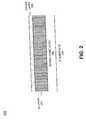
- Semiconductor device 200may include a silicon on insulator (SOI) structure that includes a silicon substrate 210 , a buried oxide layer 220 , and a silicon layer 230 on the buried oxide layer 220 .
- Buried oxide layer 220 and silicon layer 230may be formed on substrate 210 in a conventional manner.
- the thickness of buried oxide layer 220may range, for example, from about 1000 ⁇ to 4000 ⁇ .
- the thickness of silicon layer 230may range from about 200 ⁇ to 1500 ⁇ . It will be appreciated that silicon layer 230 is used to form the fin.
- substrate 210 and layer 230may include other semiconductor materials, such as germanium, or combinations of semiconductor materials, such as silicon-germanium.
- Buried oxide layer 220may include a silicon oxide or other types of dielectric materials.
- a cover layer 240may be formed on top of silicon layer 230 to aid in pattern optimization and protect silicon layer 230 during subsequent processing (act 110 ).
- Cover layer 240may, for example, include a silicon nitride material or some other type of material capable of protecting silicon layer 230 during the fabrication process.
- Cover layer 240may be deposited, for example, by chemical vapor deposition (CVD) at a thickness ranging from approximately 200 ⁇ to 500 ⁇ .
- Silicon layer 230may be patterned by conventional lithographic techniques (e.g., optical or electron beam (EB) lithography). Silicon layer 230 may then be etched using well-known etching techniques to form a wide fin 310 (act 120 ), as illustrated in FIG. 3 . Cover 240 may remain covering fin 310 .
- the width of fin 310may range from approximately 800 ⁇ to 2000 ⁇ .
- an n+ gatemay be formed (act 130 ).
- a gate dielectric material 410may be deposited or thermally grown on the side surfaces of fin 310 using known techniques, as illustrated in FIG. 4 .
- Gate dielectric material 410may include-dielectric materials, such as an SiON or high-K materials (with Hf, Zr, Y, La oxide) by atomic layer deposition (ALD) or molecular organic chemical vapor deposition (MOCVD). In other implementations, a silicon nitride or other materials may be used to form the gate dielectric.
- Gate dielectric material 410may be formed at an equivalent oxide thickness (EOT) ranging from approximately 6 ⁇ to 18 ⁇ .
- EOTequivalent oxide thickness
- a gate electrode materialmay then be deposited over semiconductor device 200 and planarized to form gate electrodes 420 adjacent gate dielectric material 410 on side surfaces of fin 310 , as illustrated in FIG. 4 .
- the gate electrode materialmay be planarized (e.g., via chemical-mechanical polishing (CMP)) to remove any gate material over the top of cover 240 , as illustrated in FIG. 4.
- CMPchemical-mechanical polishing
- a number of materialsmay be used for gate electrodes 420 .
- gate electrodes 420may include an undoped polycrystalline silicon or other types of conductive material, such as germanium or combinations of silicon and germanium. Gate electrodes 420 may be formed at a thickness ranging from approximately 1000 ⁇ to 1500 ⁇ .
- Gate electrodes 420may then be doped using a conventional implant process with tilted angles (30-45 degree) separately from the left and right sides, as illustrated in FIG. 5 .
- n-type impuritiessuch as arsenic or phosphorus
- gate electrodes 420may include silicon doped predominately, or only, with n-type impurities to form an n+ gate, as illustrated in FIG. 5 .
- the deposited gate electrode materialmay already be doped with n-type impurities.
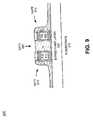
- a portion of fin 310may then be removed (act 140 ), as illustrated in FIG. 6 .
- a conventional patterning technique and etching techniquemay be used to remove a portion of cover 240 and fin 310 , while minimizing effects to the n+gate.
- the etching of fin 310may terminate on buried oxide layer 220 , as illustrated in FIG. 6, to form two separate fins 610 and 620 .
- Each of fins 610 and 620may have a width ranging from approximately 50 ⁇ to 250 ⁇ .
- the space between fins 610 and 620may range from approximately 700 ⁇ to 1500 ⁇ .
- two separate finsare formed. In other implementations, more than two fins may be formed.
- a p+ gatemay then be formed (act 150 ), as illustrated in FIGS. 7 and 8.
- a gate dielectric material 710may be thermally grown on the exposed surfaces of fins 610 and 620 , as illustrated in FIG. 7 .
- Gate dielectric 710may include a material similar to that used for gate dielectric 410 or another type of dielectric material.
- Gate dielectric material 710maybe grown to an EOT of about 6 ⁇ to about 18 ⁇ .
- Gate electrode material 720may then be deposited to fill the space between fins 610 and 620 , as illustrated in FIG. 7 .
- Gate electrode material 720may include a material similar to the material used for gate electrode 420 or another type of gate material and may be deposited to a thickness ranging from approximately 700 ⁇ to 1500 ⁇ .
- Gate electrode material 720may be doped using a conventional implant process, as illustrated in FIG. 8 .
- p-type impuritiessuch as boron or BF 2
- boron or BF 2may be implanted at a dosage of about 5 ⁇ 10 14 atoms/cm 2 to about 5 ⁇ 10 15 atoms/cm 2 and an implantation energy of about 5 KeV to about 20 KeV.
- a mask, or the likemay be used to protect other portions of semiconductor device 200 , such as the n+ gate, during the implant process.
- the deposited gate materialmay already be doped with p-type impurities.
- Gate electrode material 720may then be patterned and etched to form a gate structure.
- the resulting gate structuremay include silicon doped predominately, or only, with p-type impurities to form a p+ gate, as illustrated in FIG. 8 .
- the resulting semiconductor device 200may include two gates (i.e., n+ gate 910 and p+ gate 920 ), as illustrated in FIG. 9 .
- Conventional MOSFET fabrication processingcan then be used to complete the transistor (e.g., forming the source and drain regions), contacts, interconnects and inter-level dielectrics for the asymmetric double gate MOSFET.
- gates 910 and 920may be independently biased during circuit operation.
- FIG. 10illustrates an exemplary process for fabricating an asymmetric all-around gate MOSFET in an implementation consistent with the principles of the invention.
- FIGS. 11-18illustrate exemplary cross-sectional views of an all-around gate MOSFET fabricated according to the processing described with respect to FIG. 10 .
- Processingmay begin with semiconductor device 1100 .
- Semiconductor device 1100may include a SOI structure that includes silicon substrate 1110 , buried oxide layer 1120 , and silicon layer 1130 .
- the SOI structuremay be similar to the one described with respect to FIG. 2 .
- a cover layer 1140may be formed on top of silicon layer 1130 to aid in pattern optimization and protect silicon layer 1130 during subsequent processing (act 1010 ).
- Cover layer 1140may, for example, include a silicon nitride material or some other type of material capable of protecting silicon layer 1130 during the fabrication process.
- Cover layer 1140may be deposited, for example, by CVD at a thickness ranging from approximately 200 ⁇ to 500 ⁇ .
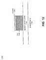
- Silicon layer 1130may be patterned by conventional lithographic techniques (e.g., optical or electron beam lithography). Silicon layer 1130 may then be etched using well-known etching techniques to form a wide fin 1210 (act 1020 ), as illustrated in FIG. 12 . Cover 1140 may remain covering fin 1210 .
- the width of fin 1210may range from approximately 800 ⁇ to 2000 ⁇ .
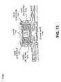
- a portion of buried oxide layer 1120may be removed using, for example, one or more conventional etching techniques (act 1030 ), as illustrated in FIG. 13 .
- buried oxide layer 1120may be etched to a depth ranging from about 1000 ⁇ to about 4000 ⁇ .
- a portion of buried oxide layer 1120 below fin 1210may be removed, as illustrated in FIG. 13 .
- the etched portion of buried oxide layer 1120may extend laterally below tin 1210 .
- the etched portionmay extend laterally below fin 1210 about half of the width of fin 1210 .
- the remaining portion of buried oxide layer 1120 located below fin 1210may be as small as about 0 ⁇ , as fin 1210 is held by silicon along the source/drain direction.
- N+ gatesmay then be formed (act 1040 ), as illustrated in FIGS. 13 and 14.
- a gate dielectric material 1310may be deposited or thermally grown using known techniques, as illustrated in FIG. 13 .
- Gate dielectric material 1310may include conventional dielectric materials, such as an oxide (e.g., silicon dioxide). In other implementations, a silicon nitride or another type of material may he used as the gate dielectric material. In yet other implementations, gate dielectric material 1310 may include a material similar to that used for gate dielectric material 410 . Gate dielectric material 1310 may be formed at a thickness ranging from approximately 6 ⁇ to 18 ⁇ .
- a gate electrode materialmay then be deposited over semiconductor device 1100 and planarized to form gate electrodes 1320 adjacent gate dielectric material 1310 on side surfaces of fin 1210 , as illustrated in FIG. 13 .
- the gate electrode materialmay be planarized (e.g., via CMP) to expose cover 1140 , as illustrated in FIG. 13.
- a number of materialsmay be used for the gate electrode material.
- the gate electrode materialmay include an undoped polycrystalline silicon or other types of conductive material, such as germanium or combinations of silicon and germanium.
- Gate electrodes 1320may be formed at a thickness ranging from approximately 1000 ⁇ to 1500 ⁇ .
- Gate electrodes 1320may then be doped using a conventional implant process with tilted angles (30-45 degree) separately from the left and right sides, as illustrated in FIG. 14 .
- n-type impuritiessuch as arsenic or phosphorus
- gate electrodes 1320may include silicon doped predominately, or only, with n-type impurities to form n+ gates, as illustrated in FIG. 14 .
- the deposited gate electrode materialmay already be doped with n-type impurities.
- a portion of fin 1210may then be removed (act 1050 ), as illustrated in FIG. 15 .
- a conventional patterning technique and etching techniquemay be used to remove a portion of cover 1140 and fin 1210 , while minimizing effects to the n+ gates.
- the etching of fin 1210may terminate on buried oxide layer 1120 , as illustrated in FIG. 15, to form two separate fins 1510 and 1520 .
- Each of fins 1510 and 1520may have a width ranging from approximately 50 ⁇ to 250 ⁇ .
- the space between fins 1510 and 1520may range from approximately 700 ⁇ to 1500 ⁇ .
- two separate finsare formed. In other implementations, more than two fins may be formed.
- a p+ gatemay then be formed (act 1060 ), as illustrated in FIGS. 16 and 17.
- a gate dielectric material 1610may be thermally grown on the exposed surfaces of fins 1510 and 1520 , as illustrated in FIG. 16 .
- Gate dielectric 1610may include a material similar to that used for gate dielectric 1310 or another type of dielectric material.
- Gate dielectric material 1610may be grown to an EOT thickness of about 6 ⁇ to about 18 ⁇ .
- Gate electrode material 1620may then be deposited to fill the space between fins 1510 and 1520 , as illustrated in FIG. 16 .
- Gate electrode material 1620may include a material similar to the material used for gate electrode material 1320 or another type of electrode material and may be deposited to a thickness ranging from approximately 700 ⁇ to 1500 ⁇ .
- Gate electrode material 1620may be doped using a conventional implant process, as illustrated in FIG. 17 .
- p-type impuritiessuch as boron or BF 2
- boron or BF 2may be implanted at a dosage of about 5 ⁇ 10 14 atoms/cm 2 to about 5 ⁇ 10 15 atoms/cm 2 and an implantation energy of about 5 KeV to about 20 KeV.
- a mask, or the likemay be used to protect portions of semiconductor device 1100 during the implant process.
- the deposited gate electrode materialmay already be doped with p-type impurities.
- Gate electrode material 1620may then be patterned and etched to form a gate structure.
- the resulting gate structuremay include silicon doped predominately, or only, with p-type impurities to form a p+ gate, as illustrated in FIG. 17 .
- the resulting semiconductor device 1100may include four (or more) gates (i.e., n+ gate 1810 , n+ gate 1820 , p+ gate 1830 , and n+ gate 1840 , as illustrated in FIG. 18 .
- N+ gate 1840may at least partially be formed under fin 1510 and/or fin 1520 .
- Conventional MOSFET fabrication processingcan then be used to complete the transistor (e.g., forming the source and drain regions), contacts, interconnects and inter-level dielectrics for the asymmetric all-around gate MOSFET.
- gates 1810 - 1840may be independently biased during circuit operation.
- FIGS. 19-24illustrate an exemplary process for forming a double gate MOSFET with asymmetric polysilicon gates.
- a fin 1930may be formed on a substrate, such as a SOI substrate that includes a silicon substrate 1910 and a buried oxide layer 1920 .
- Fin 1930may be formed using, for example, processes similar to those described above with regard to earlier implementations.
- a gate dielectric material 1940may be formed or grown on side surfaces of fin 1930 .
- a protective cap 1950may be formed over fin 1930 and gate dielectric 1940 .
- Cap 1950may include a silicon nitride and may function as a bottom antireflective coating (BARC) for subsequent processing.
- BARCbottom antireflective coating
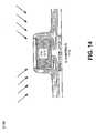
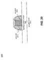
- a gate electrode materialmay then be deposited over semiconductor device 1900 and etched to form spacers 2010 and 2020 adjacent gate dielectric material 1940 on side surfaces of fin 1930 , as illustrated in FIG. 20 .
- Spacers 2010 and 2020may then be doped using a tilt angle implant process, as illustrated in FIGS. 21 and 22.
- n-type impuritiessuch as arsenic or phosphorous, may be implanted such that only a small percentage of the n-type impurities, if any, will reach spacer 2020 as the majority of spacer 2020 will be shielded from the implantation by fin 1930 and cap 1950 .
- spacer 2010comprises silicon doped predominately with, or only with, n-type impurities and spacer 2020 comprises silicon doped predominately with, or only with, p-type impurities.
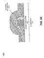
- An undoped polysilicon layer 2310may be deposited over semiconductor 1900 , as illustrated in FIG. 23 .
- Polysilicon layer 2310may then be silicided by depositing a metal, followed by an annealing to form a silicided polysilicon material 2410 , as illustrated in FIG. 24 .
- the resulting semiconductor deviceis a double gate MOSFET with asymmetrical polysilicon gates.
- FIGS. 25-28illustrate an exemplary process for forming source/drain extensions and halo implanting with the use of disposable spacers.
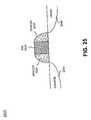
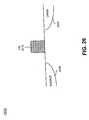
- an exemplary semiconductor device 2500may include a fin 2510 , spacers 2520 , source region 2530 , and drain region 2540 , as illustrated in FIG. 25 .
- Spacers 2520may then be removed using conventional techniques, as illustrated in FIG. 26.
- a halo implantation and source/drain extension implantationmay be performed to form halo implants and extend source region 2530 and drain region 2540 , as illustrated in FIG. 27 .
- a tilt angle implantas indicated by the arrows in FIG. 27, may be performed to form halos 2710 .
- a source/drain implantationmay then be performed to extend source/drain regions 2530 / 2540 , as illustrated in FIG. 27 .
- the removal of spacers 2520may facilitate the performance of the source/drain extension and the halo implanting.
- Spacers 2810may then be formed on side surfaces of fin 2510 , as illustrated in FIG. 28 . Conventional techniques may be used to form spacers 2810 .
- Implementations consistent with the principles of the inventionprovide asymmetric double and all-around gate FinFET devices and methods of manufacturing these devices.
- the asymmetric gatesmay be biased separately.
- logic circuitsmay be formed with the asymmetrical gate devices using less transistors than conventional circuits.
Landscapes
- Metal-Oxide And Bipolar Metal-Oxide Semiconductor Integrated Circuits (AREA)
- Thin Film Transistor (AREA)
Abstract
Description
Claims (8)
Priority Applications (1)
| Application Number | Priority Date | Filing Date | Title |
|---|---|---|---|
| US10/385,652US6800885B1 (en) | 2003-03-12 | 2003-03-12 | Asymmetrical double gate or all-around gate MOSFET devices and methods for making same |
Applications Claiming Priority (1)
| Application Number | Priority Date | Filing Date | Title |
|---|---|---|---|
| US10/385,652US6800885B1 (en) | 2003-03-12 | 2003-03-12 | Asymmetrical double gate or all-around gate MOSFET devices and methods for making same |
Publications (1)
| Publication Number | Publication Date |
|---|---|
| US6800885B1true US6800885B1 (en) | 2004-10-05 |
Family
ID=33029635
Family Applications (1)
| Application Number | Title | Priority Date | Filing Date |
|---|---|---|---|
| US10/385,652Expired - Fee RelatedUS6800885B1 (en) | 2003-03-12 | 2003-03-12 | Asymmetrical double gate or all-around gate MOSFET devices and methods for making same |
Country Status (1)
| Country | Link |
|---|---|
| US (1) | US6800885B1 (en) |
Cited By (62)
| Publication number | Priority date | Publication date | Assignee | Title |
|---|---|---|---|---|
| US20050087811A1 (en)* | 2003-10-07 | 2005-04-28 | United Microelectronics Corp. | Method for fabricating a double gate MOSFET device |
| US20050214993A1 (en)* | 2004-02-03 | 2005-09-29 | Stmicroelectronics Sa | Process for producing a field-effect transistor and transistor thus obtained |
| US20050237850A1 (en)* | 2003-10-02 | 2005-10-27 | Suman Datta | Method and apparatus for improving stability of a 6T CMOS SRAM cell |
| WO2006070309A1 (en)* | 2004-12-28 | 2006-07-06 | Koninklijke Philips Electronics N.V. | Semiconductor device having strip- shaped channel and method for manufacturing such a device |
| US20060177998A1 (en)* | 2003-09-03 | 2006-08-10 | Harrity & Snyder, L.L.P. | Fully silicided gate structure for finfet devices |
| US7091068B1 (en)* | 2002-12-06 | 2006-08-15 | Advanced Micro Devices, Inc. | Planarizing sacrificial oxide to improve gate critical dimension in semiconductor devices |
| US20060183289A1 (en)* | 2004-06-11 | 2006-08-17 | Anderson Brent A | Back gate FinFET SRAM |
| US7112847B1 (en)* | 2003-09-03 | 2006-09-26 | Advanced Micro Devices, Inc. | Smooth fin topology in a FinFET device |
| US20060223302A1 (en)* | 2005-03-31 | 2006-10-05 | Chang Peter L | Self-aligned contacts for transistors |
| WO2006122956A1 (en)* | 2005-05-19 | 2006-11-23 | International Business Machines Corporation | Fin field effect transistors (finfets) and methods for making the same |
| US20070029624A1 (en)* | 2005-08-03 | 2007-02-08 | International Business Machines Corporation | Fin-type field effect transistor |
| US20070057325A1 (en)* | 2005-09-13 | 2007-03-15 | International Business Machines Corporation | Semiconductor FinFET structures with encapsulated gate electrodes and methods for forming such semiconductor FinFET structures |
| WO2007036876A1 (en)* | 2005-09-28 | 2007-04-05 | Nxp B.V. | Double gate non-volatile memory device and method of manufacturing |
| WO2007036874A1 (en)* | 2005-09-28 | 2007-04-05 | Nxp B.V. | Finfet-based non-volatile memory device |
| US20070229417A1 (en)* | 2004-05-11 | 2007-10-04 | Koninklijke Philips Electronics, N.V. | Flexible Display Device |
| US7329913B2 (en) | 2003-12-30 | 2008-02-12 | Intel Corporation | Nonplanar transistors with metal gate electrodes |
| US7361958B2 (en) | 2004-09-30 | 2008-04-22 | Intel Corporation | Nonplanar transistors with metal gate electrodes |
| US20080111185A1 (en)* | 2006-11-13 | 2008-05-15 | International Business Machines Corporation | Asymmetric multi-gated transistor and method for forming |
| US7396711B2 (en) | 2005-12-27 | 2008-07-08 | Intel Corporation | Method of fabricating a multi-cornered film |
| CN100411143C (en)* | 2005-06-02 | 2008-08-13 | 中国科学院微电子研究所 | HVCMOS double gate oxide preparation process compatible with standard CMOS process |
| US20080206934A1 (en)* | 2007-02-23 | 2008-08-28 | Jones Robert E | Forming semiconductor fins using a sacrificial fin |
| US7449373B2 (en) | 2006-03-31 | 2008-11-11 | Intel Corporation | Method of ion implanting for tri-gate devices |
| US7456476B2 (en) | 2003-06-27 | 2008-11-25 | Intel Corporation | Nonplanar semiconductor device with partially or fully wrapped around gate electrode and methods of fabrication |
| US7479421B2 (en) | 2005-09-28 | 2009-01-20 | Intel Corporation | Process for integrating planar and non-planar CMOS transistors on a bulk substrate and article made thereby |
| US7518196B2 (en) | 2005-02-23 | 2009-04-14 | Intel Corporation | Field effect transistor with narrow bandgap source and drain regions and method of fabrication |
| US7547637B2 (en) | 2005-06-21 | 2009-06-16 | Intel Corporation | Methods for patterning a semiconductor film |
| US7550333B2 (en) | 2004-10-25 | 2009-06-23 | Intel Corporation | Nonplanar device with thinned lower body portion and method of fabrication |
| WO2009101564A1 (en)* | 2008-02-11 | 2009-08-20 | Nxp B.V. | Finfet with separate gates and method for fabricating a finfet with separate gates |
| US7579280B2 (en) | 2004-06-01 | 2009-08-25 | Intel Corporation | Method of patterning a film |
| US7736956B2 (en) | 2005-08-17 | 2010-06-15 | Intel Corporation | Lateral undercut of metal gate in SOI device |
| US20100155842A1 (en)* | 2008-12-23 | 2010-06-24 | International Business Machines Corporation | Body contacted hybrid surface semiconductor-on-insulator devices |
| US7781771B2 (en) | 2004-03-31 | 2010-08-24 | Intel Corporation | Bulk non-planar transistor having strained enhanced mobility and methods of fabrication |
| US7859053B2 (en) | 2004-09-29 | 2010-12-28 | Intel Corporation | Independently accessed double-gate and tri-gate transistors in same process flow |
| US7858481B2 (en) | 2005-06-15 | 2010-12-28 | Intel Corporation | Method for fabricating transistor with thinned channel |
| US7879675B2 (en) | 2005-03-14 | 2011-02-01 | Intel Corporation | Field effect transistor with metal source/drain regions |
| US7898041B2 (en) | 2005-06-30 | 2011-03-01 | Intel Corporation | Block contact architectures for nanoscale channel transistors |
| US20110051535A1 (en)* | 2009-09-02 | 2011-03-03 | Qualcomm Incorporated | Fin-Type Device System and Method |
| US7902014B2 (en) | 2005-09-28 | 2011-03-08 | Intel Corporation | CMOS devices with a single work function gate electrode and method of fabrication |
| US20110065244A1 (en)* | 2009-09-15 | 2011-03-17 | International Business Machines Corporation | Asymmetric finfet device with improved parasitic resistance and capacitance |
| US7915167B2 (en) | 2004-09-29 | 2011-03-29 | Intel Corporation | Fabrication of channel wraparound gate structure for field-effect transistor |
| US20110129978A1 (en)* | 2009-12-01 | 2011-06-02 | Kangguo Cheng | Method and structure for forming finfets with multiple doping regions on a same chip |
| US7960794B2 (en) | 2004-08-10 | 2011-06-14 | Intel Corporation | Non-planar pMOS structure with a strained channel region and an integrated strained CMOS flow |
| US7989280B2 (en) | 2005-11-30 | 2011-08-02 | Intel Corporation | Dielectric interface for group III-V semiconductor device |
| US8084818B2 (en) | 2004-06-30 | 2011-12-27 | Intel Corporation | High mobility tri-gate devices and methods of fabrication |
| US20120001229A1 (en)* | 2010-07-01 | 2012-01-05 | Institute of Microelectronics, Chinese Academy of Sciences | Semiconductor Device and Method for Forming the Same |
| US20120126332A1 (en)* | 2010-05-25 | 2012-05-24 | Huilong Zhu | Semiconductor device and method for forming the same |
| US20120223331A1 (en)* | 2010-07-01 | 2012-09-06 | Institute of Microelectronics, Chinese Academy of Sciences | Semiconductor device and method for forming the same |
| US8362566B2 (en) | 2008-06-23 | 2013-01-29 | Intel Corporation | Stress in trigate devices using complimentary gate fill materials |
| US20130037869A1 (en)* | 2011-08-10 | 2013-02-14 | Kabushiki Kaisha Toshiba | Semiconductor device and manufacturing method of semiconductor device |
| US8405164B2 (en) | 2003-06-27 | 2013-03-26 | Intel Corporation | Tri-gate transistor device with stress incorporation layer and method of fabrication |
| US8461650B2 (en)* | 2010-12-31 | 2013-06-11 | Institute of Microelectronics, Chinese Academy of Sciences | Semiconductor device and method for manufacturing the same |
| US8617945B2 (en) | 2006-08-02 | 2013-12-31 | Intel Corporation | Stacking fault and twin blocking barrier for integrating III-V on Si |
| CN103811338A (en)* | 2012-11-08 | 2014-05-21 | 中芯国际集成电路制造(上海)有限公司 | Semiconductor device and preparation method thereof |
| CN103928332A (en)* | 2013-01-11 | 2014-07-16 | 中芯国际集成电路制造(上海)有限公司 | Transistor and forming method thereof |
| US20140246723A1 (en)* | 2013-03-01 | 2014-09-04 | Commissariat à I'énergie atomique et aux énergies alternatives | Method for manufacturing a fin mos transistor |
| WO2014146976A1 (en)* | 2013-03-19 | 2014-09-25 | Soitec | Finfet with back-gate |
| US9349863B2 (en) | 2013-08-07 | 2016-05-24 | Globalfoundries Inc. | Anchored stress-generating active semiconductor regions for semiconductor-on-insulator finfet |
| US9583486B1 (en) | 2015-11-19 | 2017-02-28 | International Business Machines Corporation | Stable work function for narrow-pitch devices |
| CN106601618A (en)* | 2015-10-15 | 2017-04-26 | 中芯国际集成电路制造(上海)有限公司 | Semiconductor device and manufacturing method thereof and electronic device |
| US9755071B1 (en)* | 2016-06-30 | 2017-09-05 | International Business Machines Corporation | Merged gate for vertical transistors |
| US20180323284A1 (en)* | 2013-09-19 | 2018-11-08 | Taiwan Semiconductor Manufacturing Company Limited | Asymmetric semiconductor device |
| US10199503B2 (en) | 2017-04-24 | 2019-02-05 | International Business Machines Corporation | Under-channel gate transistors |
Citations (7)
| Publication number | Priority date | Publication date | Assignee | Title |
|---|---|---|---|---|
| US4317125A (en)* | 1978-05-31 | 1982-02-23 | The Secretary Of State For Defence In Her Britannic Majesty's Government Of The United Kingdom Of Great Britain And Northern Ireland | Field effect devices and their fabrication |
| US5739052A (en)* | 1994-04-08 | 1998-04-14 | Texas Instruments Incorporated | Apparatus and method for detecting defects in insulative layers of MOS active devices |
| US6458662B1 (en)* | 2001-04-04 | 2002-10-01 | Advanced Micro Devices, Inc. | Method of fabricating a semiconductor device having an asymmetrical dual-gate silicon-germanium (SiGe) channel MOSFET and a device thereby formed |
| JP2003204068A (en)* | 2001-12-14 | 2003-07-18 | Internatl Business Mach Corp <Ibm> | Implanted asymmetric doped polysilicon gate FinFET |
| US6635909B2 (en)* | 2002-03-19 | 2003-10-21 | International Business Machines Corporation | Strained fin FETs structure and method |
| US6657252B2 (en)* | 2002-03-19 | 2003-12-02 | International Business Machines Corporation | FinFET CMOS with NVRAM capability |
| US20040036118A1 (en)* | 2002-08-26 | 2004-02-26 | International Business Machines Corporation | Concurrent Fin-FET and thick-body device fabrication |
- 2003
- 2003-03-12USUS10/385,652patent/US6800885B1/ennot_activeExpired - Fee Related
Patent Citations (7)
| Publication number | Priority date | Publication date | Assignee | Title |
|---|---|---|---|---|
| US4317125A (en)* | 1978-05-31 | 1982-02-23 | The Secretary Of State For Defence In Her Britannic Majesty's Government Of The United Kingdom Of Great Britain And Northern Ireland | Field effect devices and their fabrication |
| US5739052A (en)* | 1994-04-08 | 1998-04-14 | Texas Instruments Incorporated | Apparatus and method for detecting defects in insulative layers of MOS active devices |
| US6458662B1 (en)* | 2001-04-04 | 2002-10-01 | Advanced Micro Devices, Inc. | Method of fabricating a semiconductor device having an asymmetrical dual-gate silicon-germanium (SiGe) channel MOSFET and a device thereby formed |
| JP2003204068A (en)* | 2001-12-14 | 2003-07-18 | Internatl Business Mach Corp <Ibm> | Implanted asymmetric doped polysilicon gate FinFET |
| US6635909B2 (en)* | 2002-03-19 | 2003-10-21 | International Business Machines Corporation | Strained fin FETs structure and method |
| US6657252B2 (en)* | 2002-03-19 | 2003-12-02 | International Business Machines Corporation | FinFET CMOS with NVRAM capability |
| US20040036118A1 (en)* | 2002-08-26 | 2004-02-26 | International Business Machines Corporation | Concurrent Fin-FET and thick-body device fabrication |
Non-Patent Citations (5)
| Title |
|---|
| Digh Hisamoto et al., "FinFET-A Self-Aligned Double-Gate MOSFET Scalable to 20nm," IEEE Transactions on Electron Devices, vol. 47, No. 12, Dec. 2000, pp. 2320-2325. |
| Xuejue Huang et al., "Sub 50-nm FinFET: PMOS," 1999 IEEE, IEDM, pp. 67-70. |
| Xuejue Huang et al., "Sub-50 nm P-Channel FinFET," IEEE Transactions on Electron Devices, vol. 48, No. 5, May 2001, pp. 880-886. |
| Yang-Kyu Choi et al., "Nanoscale CMOS Spacer FinFET for the Terabit Era," IEEE IEDM, Electron Device Letters, vol. 23, No. 1, Jan. 2002, pp. 25-27. |
| Yang-Kyu Choi et al., "Sub-20nm CMOS FinFET Technologies," 2001 IEEE, IEDM, pp. 421-424. |
Cited By (150)
| Publication number | Priority date | Publication date | Assignee | Title |
|---|---|---|---|---|
| US7091068B1 (en)* | 2002-12-06 | 2006-08-15 | Advanced Micro Devices, Inc. | Planarizing sacrificial oxide to improve gate critical dimension in semiconductor devices |
| US7456476B2 (en) | 2003-06-27 | 2008-11-25 | Intel Corporation | Nonplanar semiconductor device with partially or fully wrapped around gate electrode and methods of fabrication |
| US7820513B2 (en) | 2003-06-27 | 2010-10-26 | Intel Corporation | Nonplanar semiconductor device with partially or fully wrapped around gate electrode and methods of fabrication |
| US8405164B2 (en) | 2003-06-27 | 2013-03-26 | Intel Corporation | Tri-gate transistor device with stress incorporation layer and method of fabrication |
| US8273626B2 (en) | 2003-06-27 | 2012-09-25 | Intel Corporationn | Nonplanar semiconductor device with partially or fully wrapped around gate electrode and methods of fabrication |
| US7112847B1 (en)* | 2003-09-03 | 2006-09-26 | Advanced Micro Devices, Inc. | Smooth fin topology in a FinFET device |
| US20060177998A1 (en)* | 2003-09-03 | 2006-08-10 | Harrity & Snyder, L.L.P. | Fully silicided gate structure for finfet devices |
| US8008136B2 (en)* | 2003-09-03 | 2011-08-30 | Advanced Micro Devices, Inc. | Fully silicided gate structure for FinFET devices |
| US20060281236A1 (en)* | 2003-10-02 | 2006-12-14 | Suman Datta | Method and apparatus for improving stability of a 6T CMOS SRAM cell |
| US20050237850A1 (en)* | 2003-10-02 | 2005-10-27 | Suman Datta | Method and apparatus for improving stability of a 6T CMOS SRAM cell |
| US7445980B2 (en) | 2003-10-02 | 2008-11-04 | Intel Corporation | Method and apparatus for improving stability of a 6T CMOS SRAM cell |
| US7138305B2 (en)* | 2003-10-02 | 2006-11-21 | Intel Corporation | Method and apparatus for improving stability of a 6T CMOS SRAM cell |
| US20050087811A1 (en)* | 2003-10-07 | 2005-04-28 | United Microelectronics Corp. | Method for fabricating a double gate MOSFET device |
| US7423321B2 (en)* | 2003-10-07 | 2008-09-09 | United Microelectronics Corp. | Double gate MOSFET device |
| US7329913B2 (en) | 2003-12-30 | 2008-02-12 | Intel Corporation | Nonplanar transistors with metal gate electrodes |
| US20050214993A1 (en)* | 2004-02-03 | 2005-09-29 | Stmicroelectronics Sa | Process for producing a field-effect transistor and transistor thus obtained |
| US7781771B2 (en) | 2004-03-31 | 2010-08-24 | Intel Corporation | Bulk non-planar transistor having strained enhanced mobility and methods of fabrication |
| US20070229417A1 (en)* | 2004-05-11 | 2007-10-04 | Koninklijke Philips Electronics, N.V. | Flexible Display Device |
| US7579280B2 (en) | 2004-06-01 | 2009-08-25 | Intel Corporation | Method of patterning a film |
| US20060183289A1 (en)* | 2004-06-11 | 2006-08-17 | Anderson Brent A | Back gate FinFET SRAM |
| US7491589B2 (en)* | 2004-06-11 | 2009-02-17 | International Business Machines Corporation | Back gate FinFET SRAM |
| US8084818B2 (en) | 2004-06-30 | 2011-12-27 | Intel Corporation | High mobility tri-gate devices and methods of fabrication |
| US7960794B2 (en) | 2004-08-10 | 2011-06-14 | Intel Corporation | Non-planar pMOS structure with a strained channel region and an integrated strained CMOS flow |
| US7859053B2 (en) | 2004-09-29 | 2010-12-28 | Intel Corporation | Independently accessed double-gate and tri-gate transistors in same process flow |
| US7915167B2 (en) | 2004-09-29 | 2011-03-29 | Intel Corporation | Fabrication of channel wraparound gate structure for field-effect transistor |
| US8268709B2 (en) | 2004-09-29 | 2012-09-18 | Intel Corporation | Independently accessed double-gate and tri-gate transistors in same process flow |
| US8399922B2 (en) | 2004-09-29 | 2013-03-19 | Intel Corporation | Independently accessed double-gate and tri-gate transistors |
| US7361958B2 (en) | 2004-09-30 | 2008-04-22 | Intel Corporation | Nonplanar transistors with metal gate electrodes |
| US7528025B2 (en) | 2004-09-30 | 2009-05-05 | Intel Corporation | Nonplanar transistors with metal gate electrodes |
| US8067818B2 (en) | 2004-10-25 | 2011-11-29 | Intel Corporation | Nonplanar device with thinned lower body portion and method of fabrication |
| US7550333B2 (en) | 2004-10-25 | 2009-06-23 | Intel Corporation | Nonplanar device with thinned lower body portion and method of fabrication |
| US10236356B2 (en) | 2004-10-25 | 2019-03-19 | Intel Corporation | Nonplanar device with thinned lower body portion and method of fabrication |
| US8502351B2 (en) | 2004-10-25 | 2013-08-06 | Intel Corporation | Nonplanar device with thinned lower body portion and method of fabrication |
| US9741809B2 (en) | 2004-10-25 | 2017-08-22 | Intel Corporation | Nonplanar device with thinned lower body portion and method of fabrication |
| US8749026B2 (en) | 2004-10-25 | 2014-06-10 | Intel Corporation | Nonplanar device with thinned lower body portion and method of fabrication |
| US9190518B2 (en) | 2004-10-25 | 2015-11-17 | Intel Corporation | Nonplanar device with thinned lower body portion and method of fabrication |
| US20080203476A1 (en)* | 2004-12-28 | 2008-08-28 | Koninklijke Philips Electronics N.V. | Semiconductor Device Having Strip-Shaped Channel And Method For Manufacturing Such A Device |
| WO2006070309A1 (en)* | 2004-12-28 | 2006-07-06 | Koninklijke Philips Electronics N.V. | Semiconductor device having strip- shaped channel and method for manufacturing such a device |
| US7691695B2 (en)* | 2004-12-28 | 2010-04-06 | Nxp B.V. | Semiconductor device having strip-shaped channel and method for manufacturing such a device |
| US8816394B2 (en) | 2005-02-23 | 2014-08-26 | Intel Corporation | Field effect transistor with narrow bandgap source and drain regions and method of fabrication |
| US8183646B2 (en) | 2005-02-23 | 2012-05-22 | Intel Corporation | Field effect transistor with narrow bandgap source and drain regions and method of fabrication |
| US8664694B2 (en) | 2005-02-23 | 2014-03-04 | Intel Corporation | Field effect transistor with narrow bandgap source and drain regions and method of fabrication |
| US7518196B2 (en) | 2005-02-23 | 2009-04-14 | Intel Corporation | Field effect transistor with narrow bandgap source and drain regions and method of fabrication |
| US7825481B2 (en) | 2005-02-23 | 2010-11-02 | Intel Corporation | Field effect transistor with narrow bandgap source and drain regions and method of fabrication |
| US7893506B2 (en) | 2005-02-23 | 2011-02-22 | Intel Corporation | Field effect transistor with narrow bandgap source and drain regions and method of fabrication |
| US9048314B2 (en) | 2005-02-23 | 2015-06-02 | Intel Corporation | Field effect transistor with narrow bandgap source and drain regions and method of fabrication |
| US8368135B2 (en) | 2005-02-23 | 2013-02-05 | Intel Corporation | Field effect transistor with narrow bandgap source and drain regions and method of fabrication |
| US9368583B2 (en) | 2005-02-23 | 2016-06-14 | Intel Corporation | Field effect transistor with narrow bandgap source and drain regions and method of fabrication |
| US7879675B2 (en) | 2005-03-14 | 2011-02-01 | Intel Corporation | Field effect transistor with metal source/drain regions |
| US20060223302A1 (en)* | 2005-03-31 | 2006-10-05 | Chang Peter L | Self-aligned contacts for transistors |
| US7563701B2 (en) | 2005-03-31 | 2009-07-21 | Intel Corporation | Self-aligned contacts for transistors |
| WO2006122956A1 (en)* | 2005-05-19 | 2006-11-23 | International Business Machines Corporation | Fin field effect transistors (finfets) and methods for making the same |
| US7368787B2 (en) | 2005-05-19 | 2008-05-06 | International Business Machines Corporation | Fin field effect transistors (FinFETs) and methods for making the same |
| US20060261414A1 (en)* | 2005-05-19 | 2006-11-23 | International Business Machines Corporation | Fin field effect transistors (FinFETs) and methods for making the same |
| CN100411143C (en)* | 2005-06-02 | 2008-08-13 | 中国科学院微电子研究所 | HVCMOS double gate oxide preparation process compatible with standard CMOS process |
| US11978799B2 (en) | 2005-06-15 | 2024-05-07 | Tahoe Research, Ltd. | Method for fabricating transistor with thinned channel |
| US9337307B2 (en) | 2005-06-15 | 2016-05-10 | Intel Corporation | Method for fabricating transistor with thinned channel |
| US9806195B2 (en) | 2005-06-15 | 2017-10-31 | Intel Corporation | Method for fabricating transistor with thinned channel |
| US7858481B2 (en) | 2005-06-15 | 2010-12-28 | Intel Corporation | Method for fabricating transistor with thinned channel |
| US9761724B2 (en) | 2005-06-21 | 2017-09-12 | Intel Corporation | Semiconductor device structures and methods of forming semiconductor structures |
| US7547637B2 (en) | 2005-06-21 | 2009-06-16 | Intel Corporation | Methods for patterning a semiconductor film |
| US9385180B2 (en) | 2005-06-21 | 2016-07-05 | Intel Corporation | Semiconductor device structures and methods of forming semiconductor structures |
| US8581258B2 (en) | 2005-06-21 | 2013-11-12 | Intel Corporation | Semiconductor device structures and methods of forming semiconductor structures |
| US8071983B2 (en) | 2005-06-21 | 2011-12-06 | Intel Corporation | Semiconductor device structures and methods of forming semiconductor structures |
| US8933458B2 (en) | 2005-06-21 | 2015-01-13 | Intel Corporation | Semiconductor device structures and methods of forming semiconductor structures |
| US7898041B2 (en) | 2005-06-30 | 2011-03-01 | Intel Corporation | Block contact architectures for nanoscale channel transistors |
| US8524547B2 (en) | 2005-08-03 | 2013-09-03 | International Business Machines Corporation | Fin-type field effect transistor |
| US20080087968A1 (en)* | 2005-08-03 | 2008-04-17 | International Business Machines Corporation | Fin-type field effect transistor |
| US20080124868A1 (en)* | 2005-08-03 | 2008-05-29 | International Business Machines Corporation | Fin-type field effect transistor |
| US8129773B2 (en) | 2005-08-03 | 2012-03-06 | International Business Machines Corporation | Fin-type field effect transistor |
| US7348642B2 (en) | 2005-08-03 | 2008-03-25 | International Business Machines Corporation | Fin-type field effect transistor |
| US8106439B2 (en) | 2005-08-03 | 2012-01-31 | International Business Machines Corporation | Fin-type field effect transistor |
| US20070029624A1 (en)* | 2005-08-03 | 2007-02-08 | International Business Machines Corporation | Fin-type field effect transistor |
| US7736956B2 (en) | 2005-08-17 | 2010-06-15 | Intel Corporation | Lateral undercut of metal gate in SOI device |
| US7384838B2 (en)* | 2005-09-13 | 2008-06-10 | International Business Machines Corporation | Semiconductor FinFET structures with encapsulated gate electrodes and methods for forming such semiconductor FinFET structures |
| US20070057325A1 (en)* | 2005-09-13 | 2007-03-15 | International Business Machines Corporation | Semiconductor FinFET structures with encapsulated gate electrodes and methods for forming such semiconductor FinFET structures |
| US7915682B2 (en) | 2005-09-13 | 2011-03-29 | International Business Machines Corporation | Semiconductor FinFET structures with encapsulated gate electrodes and methods for forming such semiconductor FinFET structures |
| US20080048268A1 (en)* | 2005-09-13 | 2008-02-28 | International Business Machines Corporation | Semiconductor finfet structures with encapsulated gate electrodes and methods for forming such semiconductor finfet structures |
| US7902014B2 (en) | 2005-09-28 | 2011-03-08 | Intel Corporation | CMOS devices with a single work function gate electrode and method of fabrication |
| US20080203462A1 (en)* | 2005-09-28 | 2008-08-28 | Nxp B.V. | Finfet-Based Non-Volatile Memory Device |
| US7479421B2 (en) | 2005-09-28 | 2009-01-20 | Intel Corporation | Process for integrating planar and non-planar CMOS transistors on a bulk substrate and article made thereby |
| US8193567B2 (en) | 2005-09-28 | 2012-06-05 | Intel Corporation | Process for integrating planar and non-planar CMOS transistors on a bulk substrate and article made thereby |
| US20080230824A1 (en)* | 2005-09-28 | 2008-09-25 | Nxp B.V. | Double Gate Non-Volatile Memory Device and Method of Manufacturing |
| WO2007036874A1 (en)* | 2005-09-28 | 2007-04-05 | Nxp B.V. | Finfet-based non-volatile memory device |
| WO2007036876A1 (en)* | 2005-09-28 | 2007-04-05 | Nxp B.V. | Double gate non-volatile memory device and method of manufacturing |
| US8063427B2 (en) | 2005-09-28 | 2011-11-22 | Nxp B.V. | Finfet-based non-volatile memory device |
| US7791128B2 (en) | 2005-09-28 | 2010-09-07 | Nxp B.V. | Double gate non-volatile memory device and method of manufacturing |
| US8294180B2 (en) | 2005-09-28 | 2012-10-23 | Intel Corporation | CMOS devices with a single work function gate electrode and method of fabrication |
| US7989280B2 (en) | 2005-11-30 | 2011-08-02 | Intel Corporation | Dielectric interface for group III-V semiconductor device |
| US7396711B2 (en) | 2005-12-27 | 2008-07-08 | Intel Corporation | Method of fabricating a multi-cornered film |
| US7449373B2 (en) | 2006-03-31 | 2008-11-11 | Intel Corporation | Method of ion implanting for tri-gate devices |
| US8617945B2 (en) | 2006-08-02 | 2013-12-31 | Intel Corporation | Stacking fault and twin blocking barrier for integrating III-V on Si |
| US8679906B2 (en) | 2006-11-13 | 2014-03-25 | International Business Machines Corporation | Asymmetric multi-gated transistor and method for forming |
| US20080111185A1 (en)* | 2006-11-13 | 2008-05-15 | International Business Machines Corporation | Asymmetric multi-gated transistor and method for forming |
| US20100044794A1 (en)* | 2006-11-13 | 2010-02-25 | International Business Machines Corporation | Asymmetric multi-gated transistor and method for forming |
| US20080206934A1 (en)* | 2007-02-23 | 2008-08-28 | Jones Robert E | Forming semiconductor fins using a sacrificial fin |
| US7772048B2 (en)* | 2007-02-23 | 2010-08-10 | Freescale Semiconductor, Inc. | Forming semiconductor fins using a sacrificial fin |
| US8389392B2 (en) | 2008-02-11 | 2013-03-05 | Nxp B.V. | FinFET with separate gates and method for fabricating a finFET with separate gates |
| WO2009101564A1 (en)* | 2008-02-11 | 2009-08-20 | Nxp B.V. | Finfet with separate gates and method for fabricating a finfet with separate gates |
| US20100314684A1 (en)* | 2008-02-11 | 2010-12-16 | Nxp B.V. | Finfet with separate gates and method for fabricating a finfet with separate gates |
| US8362566B2 (en) | 2008-06-23 | 2013-01-29 | Intel Corporation | Stress in trigate devices using complimentary gate fill materials |
| US9806193B2 (en) | 2008-06-23 | 2017-10-31 | Intel Corporation | Stress in trigate devices using complimentary gate fill materials |
| US9224754B2 (en) | 2008-06-23 | 2015-12-29 | Intel Corporation | Stress in trigate devices using complimentary gate fill materials |
| US9450092B2 (en) | 2008-06-23 | 2016-09-20 | Intel Corporation | Stress in trigate devices using complimentary gate fill materials |
| US8741733B2 (en) | 2008-06-23 | 2014-06-03 | Intel Corporation | Stress in trigate devices using complimentary gate fill materials |
| US8962398B2 (en) | 2008-12-23 | 2015-02-24 | International Business Machines Corporation | Body contacted hybrid surface semiconductor-on-insulator devices |
| US9023694B2 (en) | 2008-12-23 | 2015-05-05 | International Business Machines Corporation | Body contacted hybrid surface semiconductor-on-insulator devices |
| US20100155842A1 (en)* | 2008-12-23 | 2010-06-24 | International Business Machines Corporation | Body contacted hybrid surface semiconductor-on-insulator devices |
| US8227867B2 (en) | 2008-12-23 | 2012-07-24 | International Business Machines Corporation | Body contacted hybrid surface semiconductor-on-insulator devices |
| US8796777B2 (en) | 2009-09-02 | 2014-08-05 | Qualcomm Incorporated | Fin-type device system and method |
| WO2011028796A1 (en)* | 2009-09-02 | 2011-03-10 | Qualcomm Incorporated | Fin-type device system and method |
| US9698267B2 (en) | 2009-09-02 | 2017-07-04 | Qualcomm Incorporated | Fin-type device system and method |
| US20110051535A1 (en)* | 2009-09-02 | 2011-03-03 | Qualcomm Incorporated | Fin-Type Device System and Method |
| CN102576730A (en)* | 2009-09-02 | 2012-07-11 | 高通股份有限公司 | Fin-type device system and method |
| CN102576730B (en)* | 2009-09-02 | 2016-02-03 | 高通股份有限公司 | Fin-type device system and method |
| US20110065244A1 (en)* | 2009-09-15 | 2011-03-17 | International Business Machines Corporation | Asymmetric finfet device with improved parasitic resistance and capacitance |
| US8138030B2 (en) | 2009-09-15 | 2012-03-20 | International Business Machines Corporation | Asymmetric finFET device with improved parasitic resistance and capacitance |
| US20110129978A1 (en)* | 2009-12-01 | 2011-06-02 | Kangguo Cheng | Method and structure for forming finfets with multiple doping regions on a same chip |
| US8021949B2 (en)* | 2009-12-01 | 2011-09-20 | International Business Machines Corporation | Method and structure for forming finFETs with multiple doping regions on a same chip |
| US8896062B2 (en)* | 2010-05-25 | 2014-11-25 | Institute of Microelectronics, Chinese Academy of Sciences | Semiconductor device and method for forming the same |
| US20120126332A1 (en)* | 2010-05-25 | 2012-05-24 | Huilong Zhu | Semiconductor device and method for forming the same |
| US20120001229A1 (en)* | 2010-07-01 | 2012-01-05 | Institute of Microelectronics, Chinese Academy of Sciences | Semiconductor Device and Method for Forming the Same |
| US8598662B2 (en)* | 2010-07-01 | 2013-12-03 | Institute of Microelectronics, Chinese Academy of Sciences | Semiconductor device and method for forming the same |
| US20120223331A1 (en)* | 2010-07-01 | 2012-09-06 | Institute of Microelectronics, Chinese Academy of Sciences | Semiconductor device and method for forming the same |
| US8816392B2 (en)* | 2010-07-01 | 2014-08-26 | Institute of Microelectronics, Chinese Academy of Sciences | Semiconductor device having gate structures to reduce the short channel effects |
| US8461650B2 (en)* | 2010-12-31 | 2013-06-11 | Institute of Microelectronics, Chinese Academy of Sciences | Semiconductor device and method for manufacturing the same |
| US20130037869A1 (en)* | 2011-08-10 | 2013-02-14 | Kabushiki Kaisha Toshiba | Semiconductor device and manufacturing method of semiconductor device |
| US8791028B2 (en)* | 2011-08-10 | 2014-07-29 | Kabushiki Kaisha Toshiba | Semiconductor device and manufacturing method of semiconductor device |
| CN103811338A (en)* | 2012-11-08 | 2014-05-21 | 中芯国际集成电路制造(上海)有限公司 | Semiconductor device and preparation method thereof |
| CN103811338B (en)* | 2012-11-08 | 2016-12-21 | 中芯国际集成电路制造(上海)有限公司 | A kind of semiconductor device and preparation method thereof |
| CN103928332B (en)* | 2013-01-11 | 2016-08-31 | 中芯国际集成电路制造(上海)有限公司 | Transistor and forming method thereof |
| CN103928332A (en)* | 2013-01-11 | 2014-07-16 | 中芯国际集成电路制造(上海)有限公司 | Transistor and forming method thereof |
| US9673329B2 (en) | 2013-03-01 | 2017-06-06 | Stmicroelectronics Sa | Method for manufacturing a fin MOS transistor |
| US20140246723A1 (en)* | 2013-03-01 | 2014-09-04 | Commissariat à I'énergie atomique et aux énergies alternatives | Method for manufacturing a fin mos transistor |
| US9236478B2 (en)* | 2013-03-01 | 2016-01-12 | Stmicroelectronics Sa | Method for manufacturing a fin MOS transistor |
| WO2014146976A1 (en)* | 2013-03-19 | 2014-09-25 | Soitec | Finfet with back-gate |
| FR3003691A1 (en)* | 2013-03-19 | 2014-09-26 | Soitec Silicon On Insulator | FINFET WITH REAR GRILLE |
| US9349863B2 (en) | 2013-08-07 | 2016-05-24 | Globalfoundries Inc. | Anchored stress-generating active semiconductor regions for semiconductor-on-insulator finfet |
| US9991366B2 (en) | 2013-08-07 | 2018-06-05 | Globalfoundries Inc. | Anchored stress-generating active semiconductor regions for semiconductor-on-insulator FinFET |
| US10734503B2 (en)* | 2013-09-19 | 2020-08-04 | Taiwan Semiconductor Manufacturing Company Limited | Asymmetric semiconductor device |
| US20180323284A1 (en)* | 2013-09-19 | 2018-11-08 | Taiwan Semiconductor Manufacturing Company Limited | Asymmetric semiconductor device |
| CN106601618A (en)* | 2015-10-15 | 2017-04-26 | 中芯国际集成电路制造(上海)有限公司 | Semiconductor device and manufacturing method thereof and electronic device |
| CN106601618B (en)* | 2015-10-15 | 2019-12-10 | 中芯国际集成电路制造(上海)有限公司 | semiconductor device, manufacturing method thereof and electronic device |
| US10170576B2 (en) | 2015-11-19 | 2019-01-01 | International Business Machines Corporation | Stable work function for narrow-pitch devices |
| US9735250B2 (en) | 2015-11-19 | 2017-08-15 | International Business Machines Corporation | Stable work function for narrow-pitch devices |
| US9583486B1 (en) | 2015-11-19 | 2017-02-28 | International Business Machines Corporation | Stable work function for narrow-pitch devices |
| US10224249B2 (en)* | 2016-06-30 | 2019-03-05 | International Business Machines Corporation | Merged gate for vertical transistors |
| US20180005902A1 (en)* | 2016-06-30 | 2018-01-04 | International Business Machines Corporation | Merged gate for vertical transistors |
| US9755071B1 (en)* | 2016-06-30 | 2017-09-05 | International Business Machines Corporation | Merged gate for vertical transistors |
| US10199503B2 (en) | 2017-04-24 | 2019-02-05 | International Business Machines Corporation | Under-channel gate transistors |
Similar Documents
| Publication | Publication Date | Title |
|---|---|---|
| US6800885B1 (en) | Asymmetrical double gate or all-around gate MOSFET devices and methods for making same | |
| US7259425B2 (en) | Tri-gate and gate around MOSFET devices and methods for making same | |
| US12021143B2 (en) | P-type strained channel in a fin field effect transistor (FinFET) device | |
| US6787406B1 (en) | Systems and methods for forming dense n-channel and p-channel fins using shadow implanting | |
| US9601598B2 (en) | Method of manufacturing a fin-like field effect transistor (FinFET) device | |
| US7781810B1 (en) | Germanium MOSFET devices and methods for making same | |
| TWI415263B (en) | Semiconductor device and method of manufacturing same | |
| US8445340B2 (en) | Sacrificial offset protection film for a FinFET device | |
| US20190109235A1 (en) | Fin-type field effect transistor structure and manufacturing method thereof | |
| US20070063224A1 (en) | Metal insulator semiconductor field effect transistor having fin structure | |
| US20140167120A1 (en) | Methods of forming a finfet semiconductor device by performing an epitaxial growth process | |
| CN1510756A (en) | Double gate field effect transistor and its manufacturing method | |
| US11862467B2 (en) | Semiconductor structure and method of manufacturing the same | |
| US6924561B1 (en) | SRAM formation using shadow implantation | |
| US6914277B1 (en) | Merged FinFET P-channel/N-channel pair | |
| US7064022B1 (en) | Method of forming merged FET inverter/logic gate | |
| US20240363435A1 (en) | Structure and method for finfet device with source/drain modulation | |
| US7262104B1 (en) | Selective channel implantation for forming semiconductor devices with different threshold voltages | |
| US10741685B2 (en) | Semiconductor devices having a fin channel arranged between source and drift regions and methods of manufacturing the same | |
| US20060228862A1 (en) | Fet design with long gate and dense pitch | |
| US9502561B1 (en) | Semiconductor devices and methods of forming the same | |
| US12324217B2 (en) | Laterally diffused metal-oxide semiconductor with gate contact | |
| US20240274669A1 (en) | Structure and Method for High-Voltage Device | |
| US20240349476A1 (en) | Semiconductor device and method of fabricating the same | |
| US20250126818A1 (en) | Structure and method for high-voltage device |
Legal Events
| Date | Code | Title | Description |
|---|---|---|---|
| AS | Assignment | Owner name:ADVANCED MICRO DEVICES, INC., CALIFORNIA Free format text:ASSIGNMENT OF ASSIGNORS INTEREST;ASSIGNORS:AN, JUDY XILIN;YU, BIN;REEL/FRAME:013870/0781 Effective date:20030206 | |
| FEPP | Fee payment procedure | Free format text:PAYOR NUMBER ASSIGNED (ORIGINAL EVENT CODE: ASPN); ENTITY STATUS OF PATENT OWNER: LARGE ENTITY | |
| FPAY | Fee payment | Year of fee payment:4 | |
| AS | Assignment | Owner name:GLOBALFOUNDRIES INC., CAYMAN ISLANDS Free format text:AFFIRMATION OF PATENT ASSIGNMENT;ASSIGNOR:ADVANCED MICRO DEVICES, INC.;REEL/FRAME:023119/0083 Effective date:20090630 | |
| FPAY | Fee payment | Year of fee payment:8 | |
| REMI | Maintenance fee reminder mailed | ||
| LAPS | Lapse for failure to pay maintenance fees | ||
| STCH | Information on status: patent discontinuation | Free format text:PATENT EXPIRED DUE TO NONPAYMENT OF MAINTENANCE FEES UNDER 37 CFR 1.362 | |
| FP | Lapsed due to failure to pay maintenance fee | Effective date:20161005 | |
| AS | Assignment | Owner name:GLOBALFOUNDRIES U.S. INC., NEW YORK Free format text:RELEASE BY SECURED PARTY;ASSIGNOR:WILMINGTON TRUST, NATIONAL ASSOCIATION;REEL/FRAME:056987/0001 Effective date:20201117 |