US6798223B2 - Test methods, systems, and probes for high-frequency wireless-communications devices - Google Patents
Test methods, systems, and probes for high-frequency wireless-communications devicesDownload PDFInfo
- Publication number
- US6798223B2 US6798223B2US09/725,646US72564600AUS6798223B2US 6798223 B2US6798223 B2US 6798223B2US 72564600 AUS72564600 AUS 72564600AUS 6798223 B2US6798223 B2US 6798223B2
- Authority
- US
- United States
- Prior art keywords
- probe
- ground
- signal
- test
- contact
- Prior art date
- Legal status (The legal status is an assumption and is not a legal conclusion. Google has not performed a legal analysis and makes no representation as to the accuracy of the status listed.)
- Expired - Fee Related
Links
- 239000000523sampleSubstances0.000titleclaimsabstractdescription155
- 238000004891communicationMethods0.000titleclaimsdescription11
- 238000010998test methodMethods0.000titleclaimsdescription5
- 238000012360testing methodMethods0.000claimsabstractdescription103
- 238000000034methodMethods0.000claimsdescription19
- 239000004020conductorSubstances0.000claimsdescription7
- 230000008878couplingEffects0.000claimsdescription2
- 238000010168coupling processMethods0.000claimsdescription2
- 238000005859coupling reactionMethods0.000claimsdescription2
- 238000005259measurementMethods0.000claims2
- 230000005684electric fieldEffects0.000claims1
- 230000000712assemblyEffects0.000description14
- 238000000429assemblyMethods0.000description14
- 239000000758substrateSubstances0.000description9
- 230000007246mechanismEffects0.000description3
- PXHVJJICTQNCMI-UHFFFAOYSA-NNickelChemical compound[Ni]PXHVJJICTQNCMI-UHFFFAOYSA-N0.000description2
- 239000000969carrierSubstances0.000description2
- 238000004519manufacturing processMethods0.000description2
- XAGFODPZIPBFFR-UHFFFAOYSA-NaluminiumChemical compound[Al]XAGFODPZIPBFFR-UHFFFAOYSA-N0.000description1
- 229910052782aluminiumInorganic materials0.000description1
- 230000002950deficientEffects0.000description1
- 238000009826distributionMethods0.000description1
- 230000009977dual effectEffects0.000description1
- 230000000694effectsEffects0.000description1
- 239000010931goldSubstances0.000description1
- 229910052737goldInorganic materials0.000description1
- 229910052759nickelInorganic materials0.000description1
- 230000003287optical effectEffects0.000description1
- 230000010355oscillationEffects0.000description1
- 230000003071parasitic effectEffects0.000description1
- 230000002093peripheral effectEffects0.000description1
- 238000007747platingMethods0.000description1
- 239000007787solidSubstances0.000description1
- 238000012956testing procedureMethods0.000description1
- 239000002699waste materialSubstances0.000description1
Images


Classifications
- G—PHYSICS
- G01—MEASURING; TESTING
- G01R—MEASURING ELECTRIC VARIABLES; MEASURING MAGNETIC VARIABLES
- G01R31/00—Arrangements for testing electric properties; Arrangements for locating electric faults; Arrangements for electrical testing characterised by what is being tested not provided for elsewhere
- G01R31/28—Testing of electronic circuits, e.g. by signal tracer
- G01R31/282—Testing of electronic circuits specially adapted for particular applications not provided for elsewhere
- G01R31/2822—Testing of electronic circuits specially adapted for particular applications not provided for elsewhere of microwave or radiofrequency circuits
- G—PHYSICS
- G01—MEASURING; TESTING
- G01R—MEASURING ELECTRIC VARIABLES; MEASURING MAGNETIC VARIABLES
- G01R1/00—Details of instruments or arrangements of the types included in groups G01R5/00 - G01R13/00 and G01R31/00
- G01R1/02—General constructional details
- G01R1/06—Measuring leads; Measuring probes
- G01R1/067—Measuring probes
- G01R1/06772—High frequency probes
Definitions
- the present inventionconcerns testing equipment and methods for high-frequency devices, particularly test probes for wireless communications devices.
- a multi-tiered electronic assemblywhich includes an integrated-circuit chip, a chip carrier, and a main circuit board.
- the chipis soldered onto one side of the larger, and sturdier, chip carrier.
- the other side of the chip carrieris soldered to the main circuit board, sandwiching the chip carrier between the chip and the main circuit board.
- the main circuit boardknown as a motherboard, includes circuitry that electrically communicates with the chip through conductors inside and on the surface of the chip carrier.
- the conventional testing proceduretests each motherboard with the chip and chip carrier mounted to it. This testing, which is typically done manually, entails using test probes not only to apply test signals to inputs of the motherboard, but also to measure output signals at its outputs. A network analyzer, coupled to the test probe at the outputs, shows whether the output signals are acceptable or unacceptable. Unacceptable assemblies are generally discarded, because of the difficulty in salvaging the chip, chip carrier, or motherboard for reuse.
- GSGground-signal-ground
- PICOPROBEbrand test probe from GGB Industries.
- PICOBROBEappears to be a trademark of GGB Industries.
- U.S. Pat. No. 5,565,788Another example is shown in U.S. Pat. No. 5,565,788.
- the first problemis that proper probe operation requires the device under test, such as a motherboard assembly, include at least two ground pads, or contacts, next to each signal port being tested.
- the ground contactsengage the ground probe tips at the sides of the signal probe tip to shield the probe from electrical interference during testing.
- these adjacent ground padscan generate parasitic resonances which frustrate normal operation of the devices.
- the second problemis that conventional test methods only test complete motherboard assemblies—that is motherboards with mounted chips and chip carriers. Because of the difficulty in separating chip carriers from motherboards, defective motherboard assemblies are discarded as waste, increasing manufacturing cost.
- One unique probe structureincludes at least one signal contact surface for contacting a signal-port trace of an electronic assembly and at least one ground contact surface for contacting a ground pad of the electronic assembly, with the ground contact surface substantially larger than the signal contact surface.
- Another unique probe structureincludes at least one signal contact surface for contacting the signal-port trace and a ground probe having a contact surface for contacting the ground pad and a non-contact surface for overhanging a portion of the contacted signal-port trace and thereby establishing a characteristic impedance.
- Other unique probe structuresinclude not only the larger ground contact surface or the ground with a non-contact surface, but also contacts for communicating electrical bias signals to devices under test.
- One exemplary systemmounts one or more of the unique probe structures to a programmable XYZ table to facilitate rapid testing of chip-carrier assemblies.
- one exemplary methodentails testing one or more millimeter-wave chip-carrier assemblies using a unique probe structure prior to mounting the assembly to a main circuit board, such as a motherboard.
- FIG. 1is a bottom perspective view of a high-frequency test head 100 incorporating teachings of the present invention.
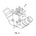
- FIG. 2is top perspective view of exemplary test head 100 in FIG. 1 .
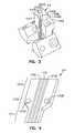
- FIG. 3is a top perspective view of probe-support fixture 110 , a component of test head 100 .
- FIG. 4is a back perspective view of front plate 117 , another component of test head 100 .
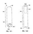
- FIG. 5.1is a perspective view of a central ground probe 160 , one component of test head 100 .
- FIG. 5.2is a cross-sectional view of central ground probe 160 taken along line 2 — 2 in FIG. 5.1.
- FIG. 6is a perspective view of test head 100 in overhead alignment with an exemplary chip-carrier assembly 600 .
- FIG. 7is a simplified cross-sectional view of test head 100 in contact with signal port traces 611 and 612 and ground pad 614 of chip-carrier assembly 600 .
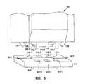
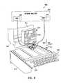
- FIG. 8is a perspective view of an exemplary test system 800 which incorporates exemplary test head 100 .
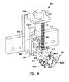
- FIG. 9is a perspective view of a z-axis translator 818 , one component of test system 800 in FIG. 8 .
- FIGS. 1-9describes and illustrates specific embodiments of the invention. These embodiments, offered not to limit but only to exemplify and teach the concepts of the invention, are shown and described in sufficient detail to enable those skilled in the art to make and use the invention. Thus, where appropriate to avoid obscuring the invention, the description may omit certain information known to those of skill in the art.
- FIG. 1a bottom perspective view, shows an exemplary high-frequency test head 100 which incorporates teachings of the present invention.
- Test head 100includes a probe-support fixture 110 , left and right signal probes 120 and 130 , front and back DC probes 140 and 150 , and a central ground probe 160 .
- Probe-support fixture 110holds probes 120 - 160 in a fixed spatial relationship that corresponds to the input-output arrangement of a high-frequency chip-carrier assembly (not shown in this view.)
- Left and right signal probes 120 and 130include respective coaxial couplings 122 and 132 , and signal probe tips 124 and 134 .
- Front DC probe 140includes front DC probe tips 142 . 1 , 142 . 2 , and 142 .
- Central ground probe 160includes a ground offset (or non-contact) surface 166 . 1 and a ground contact 166 . 2 .
- probe-support fixture 110which is electrically insulated from probe tips 124 and 134 and DC probes 140 and 150 , includes left and right portions 112 and 116 , a center portion 114 , and a front plate 117 .
- Left portion 112which supports left signal probe 120 , includes a bottom face 112 . 1 and a tuning conductor 112 . 2
- right portion 116which supports right signal probe 130 , includes a bottom face 116 . 1 and a tuning conductor 116 . 2 .
- Bottom face 112 . 1includes notches 112 . 11 and 112 . 12 and a hole 112 . 13 , which are linked via a transverse through-hole 112 .
- bottom face 116 . 1includes notches 116 . 11 and 116 . 12 and a hole 116 . 13 , which are linked via a transverse through-hole 116 . 14 for tuning conductor 116 . 2 .
- FIG. 2a top perspective view of test head 100 , shows that center portion 114 includes a central bore 114 . 1 which directly contacts ground probe 160 .
- a screw 164 . 2 in probe 160facilitates rotation of probe 160 within bore 114 . 1
- a set screw 114 . 3fixes the vertical and angular position of ground probe 160 within center portion 114 of fixture 110 .
- set screw 114 . 3allows one to replace ground probe 160 with another ground probe providing a different characteristic impedance or the same characteristic impedance for a different device under test.
- Holes 114 . 4 and 114 . 5are used for mounting the test head to an actuation assembly as shown in FIGS. 6 and 7.
- FIG. 3a top perspective view of probe-support structure 110 , shows that center portion 114 further includes front and back surfaces 114 . 6 and 114 . 7 which confront respective interior surfaces of front plate 117 and a back plate 118 (shown in FIG. 2.)
- Front surface 114 . 6includes substantially parallel grooves 114 . 61 , 114 . 62 , and 114 . 63 .
- Back surface 114 . 7includes substantially parallel grooves 114 . 71 , 114 . 72 , and 114 . 73 .
- FIG. 4shows a perspective view of front plate 117 , which is structurally identical to back plate 118 .
- Front plate 117includes respective narrow, broad, and intermediate sections 117 . 1 , 117 . 2 , and 117 . 3 as well as parallel grooves 117 . 4 117 . 5 , and 117 . 6 .
- Narrow section 117 . 1terminates in a 45-degree bevel;
- intermediate section 117 . 2includes holes 117 . 21 and 117 . 22 and tapers at 45 degrees from narrow section 117 . 1 to broad section 117 . 3 .
- Grooves 117 . 4 , 117 . 5 , and 117 . 6correspond to those of front surface 114 . 6 .
- Front DC bias feeds 144 . 1 , 144 . 2 , and 144 . 3are sandwiched respectively between grooves 11 . 71 , 114 . 72 , and 114 . 73 and grooves 117 . 4 , 117 . 5 , and 117 . 6 .
- back DC bias feeds 154 . 1 , 154 . 2 , and 154 . 3are sandwiched respectively between grooves 114 . 71 , 114 . 72 , and 114 . 73 of the back surface 114 . 7 and corresponding grooves (not shown) in back plate 118 (in FIG. 2 ).
- FIGS. 5.1 and 5 . 2show respective perspective and cross-sectional views of central ground probe 160 .
- Ground probe 160includes a conductive cylindrical shaft 162 of substantially uniform diameter of 0.125 inches (3.17 millimeters) for example.
- Shaft 162has an upper portion 164 and a lower portion 166 .
- Upper portion 164includes a central axial bore 164 . 1 and a screw 164 . 2 .
- Screw 164 . 2allows one to adjust the angular orientation of probe 160 relative to other portions of probe 100 .
- axial bore 164 . 1has an approximate diameter of 0.10 inches (2.50 millimeters) and an approximate depth of 0.20 inches (7.88 millimeters.)
- Lower portion 166includes a ground offset surface 166 .
- Ground contact surface 166 . 2 in the exemplary embodimentis a rectangular solid, with an exemplary depth of about 0.0045 inches (0.114 millimeters), an exemplary length of about 0.082 inches (2.08 millimeters), and an exemplary width of about 0.048 inches (1.22 millimeters.)
- ground contact 166 . 2contacts a ground contact of a device under test that has adjacent signal ports
- a portion of ground offset surface 166 . 1overhangs a portion of an one or more of the adjacent signal port trace of the device under test.
- this arrangementestablishes a desired characteristic impedance. For example, an offset of about 4.3 mils (0.144 millimeters) with a trace width of about 18 mils (0.457 millimeters) forms a nominal characteristic impedance of 50 Ohms.
- the exemplary embodimentmachines probe-support structure 110 from aluminum 6061-T6 and finishes it with 0.00001-inch-thick, 24-carat-gold plating over 0.0002-inch-thick nickel. Front and back plates 117 and 118 , and ground probe 160 are fabricated similarly.
- FIG. 6shows how exemplary test head 100 is intended to engage a exemplary high-frequency chip-carrier assembly (or surface-mount package) 600 .
- Chip-carrier assembly 600includes a chip-carrier substrate 610 and an integrated circuit chip 620 . Though not shown, the exemplary embodiment provides chip 620 with a lid or cover for protection.
- chip-carrier substrate 610includes two high-frequency signal port traces or contacts 611 and 612 , a central ground pad 614 , and low-frequency or direct-current (DC) bias pads 617 and 618 .
- Signal-port traces 611 and 612which have a rectangular shape in this embodiment, are positioned directly opposite each other.
- Central ground pad 614which has an exemplary rectangular shape or peripheral outline, lies centered not only between signal-port traces 611 and 612 , but also between DC bias pads 617 and 618 .
- DC bias pads 617includes a collinear arrangement of three pads 617 . 1 , 617 . 2 , and 617 . 3 on one side of carrier 610
- DC bias pads 618includes a collinear arrangement of three pads 618 . 1 , 618 . 2 , and 618 . 3 .
- FIG. 6further shows that various portions of test head 100 are aligned with portions of chip-carrier assembly 600 .
- left and right signal probe tips 124 and 134are aligned to contact respective signal port traces 611 and 612
- front (and back) DC bias probe tips 142 . 1 , 142 . 2 , 142 . 3are aligned to contact DC bias pads 617 . 1 , 617 . 2 , and 617 . 3
- central ground probe 160is aligned to contact central ground pad 614 .
- the figuredoes not clearly show alignment of back DC bias probe tips 152 . 1 , 152 . 2 , 152 . 3 with DC bias pads 618 . 1 , 618 . 2 , and 618 . 3 , although this is what is intended in the exemplary embodiment.
- ground contact 166 . 2register precisely with pad 614 .
- FIG. 7shows a simplified cross-sectional view of left and right signal probes 120 and 130 and ground probe 160 of test head 100 in contact respectively with signal port traces 611 and 612 and ground pad 614 .
- ground contact 166 . 2contacts ground pad 614
- left and right portions of ground offset surface 166 . 1overhang respective portions of signal port traces 611 and 612 .
- this arrangementsets a desired characteristic impedance between ground surface and the signal port trace.
- a depth of 0.0043 inches (0.114 millimeters)sets a characteristic impedance of 50 ohms.
- Replacement of the ground probe with anotherallows one to reconfigure the test head for other characteristic impedances, and/or electronic assemblies with other contact distributions, shapes, and/or dimensions.
- ground contact 166 . 2provides ground contact 166 . 2 as a set of two or more ground contact points. Variants of these embodiments form the ground contact points in hemispherical or conic forms. Still other embodiments provide the ground contact points as a set of angled fingers, similar in form to probe tips 124 and 134 to cushion impact of test head 100 with chip-carrier assembly 600 . Other embodiments may combine rigid or resilient contacts with one or more other resilient conductive or nonconductive features, such a spring member, to facilitate a soft landing of the ground probe.
- ground contact surfaceis part of an axial insert within a cylindrical or rectangular ground sleeve.
- the ground sleevehas an end face which functions as an offset surface, and the axial insert slides within the sleeve, allowing one to adjust and set the distance between the offset surface and the contact surface and thus to set the characteristic impedance of the probe.
- Other more complex fine tuning mechanismsare also feasible with this variable mechanism. Indeed, with an automated adjustment mechanism and suitable feedback electronics, it is conceivable to dynamically match the characteristic impedance of the probe to each device under test in a mass-production environment using an automated test system.
- FIG. 8shows an exemplary test system 800 that incorporates exemplary test head 100 .
- system 800includes a programmable XYZ table 810 , and a network analyzer 820 .
- XYZ table 810includes an x-axis translator 812 , an y-axis translator 814 , a substrate holder 816 , and a z-axis translator 818 .
- X-axis translator 812moves z-axis translator 818 along an x-axis dimension 840
- y-axis translator 814moves substrate holder 816 , which holds one or more exemplary chip-carrier assemblies 600 , along a y-axis dimension 842 perpendicular to the x-axis dimension.
- Z-axis translator 818which includes bias circuitry 818 . 1 coupled to the dc bias feeds of test head 100 , moves the test head along a z-axis dimension 844 , perpendicular to the x- and y-axes, to engage its probe tips with each of chip-carrier assemblies 600 on substrate holder 816 .
- Network analyzer 820includes network-analyzer ports 822 and 824 .
- a programmed computer controllercontrols XYZ table 810 , using x-axis and y-axis translators 812 and 814 to align z-axis translator 818 , more precisely test head 100 , over one of the chip-carrier assemblies on substrate holder 816 .
- the controlleroperates z-axis translator 818 to bring test head 100 , specifically signal probe tips 124 and 134 into contact with respective signal port traces 611 and 612 ; front and back DC probe tips 142 and 152 into contact with respective DC bias pads 617 and 618 ; and central ground probe 160 into contact with central ground pad 614 , as indicated in FIGS. 6 and 7.
- Some embodimentscontrol movement of the test head in the z-dimension by established a predetermined stopping point for the test head.
- Other embodimentsuse the sensed flow of electrical current through the bias circuitry as a stop signal for downward movement of the test head.
- Still other embodimentsmay force gas through a nozzle mounted adjacent the test head on to the substrate or substrate holder, sense back pressure as the test head moves downward, and cease movement when the back pressure exceeds a certain threshold.
- Yet other embodimentsmay use optical control methods.
- Control softwaresenses the flow of current through the bias feeds, and waits a predetermined period of time, for example 10 seconds, to allow for establishing a steady-state condition. Once the steady-state condition is established, the control software directs network analyzer to output a test signal, for example in the 27-32 Giga-Hertz range, from port 822 , through left signal probe 120 , and into signal-port trace 611 of chip-carrier assembly 600 .
- Assembly 600outputs a signal through signal-port trace 612 and right signal probe 130 to network-analyzer port 824 .
- Network analyzer 820measures one or more electrical properties (such as S-parameters, power, delay, and so forth), compares the one or more measured properties to acceptance criteria, and records the results of the test along with a part identifier for the chip-carrier assembly, indicating whether the assembly has passed or failed.
- the controllerthen operates the z-axis translator to disengage the test head from the chip-carrier assembly; operates the x-axis and y-axis translators to align the test head with the next chip-carrier assembly for testing.
- Those assemblies that pass the testwill be mounted to a motherboard or other circuitry using conventional mounting procedures, whereas those that fail will be discarded or salvaged.
- FIG. 9shows a perspective view of exemplary z-axis translator 818 without bias circuitry 818 . 1 .
- Translator 818includes a spring-biased vertical actuation assembly 900 , which is shown in its extended or actuated position.
- Assembly 900includes table-mount bracket 910 , an actuator bracket 920 , an actuator 930 , a test-head bracket 940 , and a bias spring 950 .
- Table-mount bracket 910which is used to fasten assembly 900 to y-axis translator 814 , is fastened or secured to left and right stem portions 922 . 1 and 922 . 2 of actuator bracket 920 .
- Actuator bracket 920which forms an inverted “L,” includes a lower stem portion 922 and an upper portion 924 .
- Stem portion 922includes a central slot 922 . 3 between left and right portions 922 . 1 and 922 . 2 .
- Fastened to upper portion 924is one end of actuator 930 .
- Actuator 930which in various embodiments is hydraulic, pneumatic, or electric, includes a rod 932 mounted to test-head mount bracket 940 .
- Test-head bracket 940forms a “T”, and includes an upper portion 942 and a lower portion 944 .
- Upper portion 942slidably engages central slot 922 . 3 .
- Lower portion 944includes a slot 944 . 1 , which defines left and right end portions 944 . 2 and 944 . 3 .
- Slot 944 . 1receives front and back DC bias feeds 144 and 154 of test head 100
- left and right end portions 944 . 2 and 944 . 3are fastened to test head 100 using its holes 114 . 4 and 114 . 5 (shown in FIG. 2 ).
- Bias spring 950which is connected between lower portion 944 and upper portion 924 of actuator bracket 920 , bias the actuator toward a disengaged position, that is, away from substrate holder 816 (in FIG. 8.)
- One unique probe structureincludes at least one signal contact surface for contacting a signal-port trace of an electronic assembly and at least one ground contact surface for contacting a ground pad of the electronic assembly, with the ground contact surface substantially larger than the signal contact surface.
- Another unique probe structureincludes a non-contact ground surface for overhanging a portion of the contacted signal-port trace and thereby establishing a characteristic impedance.
- yet anotherincludes conductors for communicating electrical bias signals to devices under test.
Landscapes
- Physics & Mathematics (AREA)
- General Physics & Mathematics (AREA)
- General Engineering & Computer Science (AREA)
- Engineering & Computer Science (AREA)
- Measuring Leads Or Probes (AREA)
- Testing Of Individual Semiconductor Devices (AREA)
- Printing Elements For Providing Electric Connections Between Printed Circuits (AREA)
- Detection And Prevention Of Errors In Transmission (AREA)
- Mobile Radio Communication Systems (AREA)
- Testing Or Measuring Of Semiconductors Or The Like (AREA)
- Radio Transmission System (AREA)
- Testing Electric Properties And Detecting Electric Faults (AREA)
- Tests Of Electronic Circuits (AREA)
Abstract
Description
The present application is a continuation of U.S. Provisional Application No. 60/221,550, which was filed on Jul. 28, 2000. This application is incorporated herein by reference.
The present invention concerns testing equipment and methods for high-frequency devices, particularly test probes for wireless communications devices.
The increasing popularity of wireless communications devices, such as mobile telephones and pagers, has placed considerable demand on the limited range of broadcast frequencies that the federal government allots for these devices. In response, the federal government has extended this range to include higher frequencies. For example, the range for these devices now includes frequencies in the range of 27-32 Giga-Hertz. (A Giga-Hertz is one billion cycles or oscillations per second.)
In turn, makers of communication devices now offer or intend to offer devices that function at these higher frequencies. At the heart of many of these devices is a multi-tiered electronic assembly, which includes an integrated-circuit chip, a chip carrier, and a main circuit board. The chip is soldered onto one side of the larger, and sturdier, chip carrier. The other side of the chip carrier is soldered to the main circuit board, sandwiching the chip carrier between the chip and the main circuit board. The main circuit board, known as a motherboard, includes circuitry that electrically communicates with the chip through conductors inside and on the surface of the chip carrier.
One important aspect in making these multi-tiered electronic assemblies is testing their electrical capabilities. The conventional testing procedure tests each motherboard with the chip and chip carrier mounted to it. This testing, which is typically done manually, entails using test probes not only to apply test signals to inputs of the motherboard, but also to measure output signals at its outputs. A network analyzer, coupled to the test probe at the outputs, shows whether the output signals are acceptable or unacceptable. Unacceptable assemblies are generally discarded, because of the difficulty in salvaging the chip, chip carrier, or motherboard for reuse.
One conventional type of test probe that is considered suitable for testing high-frequency electronic assemblies is the ground-signal-ground (GSG) single or dual signal-port probe. This probe type places each signal probe tip between two grounded probe tips, which electrically shield the signal probe tip during testing. The ends of the ground and signal tips—that is, the ends which contact the device under test—are substantially identical in structure, each having a sharp pointed end to facilitate its precise placement on conductive portions of the device under test. One example of this type probe is the PICOPROBE brand test probe from GGB Industries. (PICOBROBE appears to be a trademark of GGB Industries.) Another example is shown in U.S. Pat. No. 5,565,788.
There are at least two problems that the present inventors have recognized with high-frequency applications of conventional test probes and test methods. The first problem is that proper probe operation requires the device under test, such as a motherboard assembly, include at least two ground pads, or contacts, next to each signal port being tested. The ground contacts engage the ground probe tips at the sides of the signal probe tip to shield the probe from electrical interference during testing. However, at high frequencies, these adjacent ground pads can generate parasitic resonances which frustrate normal operation of the devices.
The second problem is that conventional test methods only test complete motherboard assemblies—that is motherboards with mounted chips and chip carriers. Because of the difficulty in separating chip carriers from motherboards, defective motherboard assemblies are discarded as waste, increasing manufacturing cost.
Accordingly, there is a need for better test probes and testing methods for high-frequency electronic assemblies.
To address this and other needs, the present inventors have devised unique test probes for testing high-frequency electronic assemblies, such as those for wireless communications devices. One unique probe structure includes at least one signal contact surface for contacting a signal-port trace of an electronic assembly and at least one ground contact surface for contacting a ground pad of the electronic assembly, with the ground contact surface substantially larger than the signal contact surface. Another unique probe structure includes at least one signal contact surface for contacting the signal-port trace and a ground probe having a contact surface for contacting the ground pad and a non-contact surface for overhanging a portion of the contacted signal-port trace and thereby establishing a characteristic impedance. Other unique probe structures include not only the larger ground contact surface or the ground with a non-contact surface, but also contacts for communicating electrical bias signals to devices under test.
Other aspects of the invention include systems and methods that incorporate one or more of unique probe structures. One exemplary system mounts one or more of the unique probe structures to a programmable XYZ table to facilitate rapid testing of chip-carrier assemblies. And, one exemplary method entails testing one or more millimeter-wave chip-carrier assemblies using a unique probe structure prior to mounting the assembly to a main circuit board, such as a motherboard.
FIG. 1 is a bottom perspective view of a high-frequency test head 100 incorporating teachings of the present invention.
FIG. 2 is top perspective view ofexemplary test head 100 in FIG.1.
FIG. 3 is a top perspective view of probe-support fixture 110, a component oftest head 100.
FIG. 4 is a back perspective view offront plate 117, another component oftest head 100.
FIG. 5.1 is a perspective view of acentral ground probe 160, one component oftest head 100.
FIG. 5.2 is a cross-sectional view ofcentral ground probe 160 taken alongline 2—2 in FIG. 5.1.
FIG. 6 is a perspective view oftest head 100 in overhead alignment with an exemplary chip-carrier assembly 600.
FIG. 7 is a simplified cross-sectional view oftest head 100 in contact withsignal port traces ground pad 614 of chip-carrier assembly 600.
FIG. 8 is a perspective view of anexemplary test system 800 which incorporatesexemplary test head 100.
FIG. 9 is a perspective view of a z-axis translator 818, one component oftest system 800 in FIG.8.
The following detailed description, which references and incorporates FIGS. 1-9, describes and illustrates specific embodiments of the invention. These embodiments, offered not to limit but only to exemplify and teach the concepts of the invention, are shown and described in sufficient detail to enable those skilled in the art to make and use the invention. Thus, where appropriate to avoid obscuring the invention, the description may omit certain information known to those of skill in the art.
FIG. 1, a bottom perspective view, shows an exemplary high-frequency test head 100 which incorporates teachings of the present invention.Test head 100 includes a probe-support fixture 110, left andright signal probes back DC probes central ground probe 160. Probe-support fixture 110 holds probes120-160 in a fixed spatial relationship that corresponds to the input-output arrangement of a high-frequency chip-carrier assembly (not shown in this view.) Left andright signal probes coaxial couplings signal probe tips Front DC probe 140 includes front DC probe tips142.1,142.2, and142.3 which are coupled to respective DC bias feeds144.1,144.2,144.3, andback DC probe 150 includes back DC probe tips152.1,152.2, and152.3 which are coupled to respective back DC bias feeds154.1,154.2, and154.3.Central ground probe 160 includes a ground offset (or non-contact) surface166.1 and a ground contact166.2.
More particularly, probe-support fixture 110, which is electrically insulated fromprobe tips right portions center portion 114, and afront plate 117.Left portion 112, which supports leftsignal probe 120, includes a bottom face112.1 and a tuning conductor112.2, andright portion 116, which supportsright signal probe 130, includes a bottom face116.1 and a tuning conductor116.2. Bottom face112.1 includes notches112.11 and112.12 and a hole112.13, which are linked via a transverse through-hole112.14 for tuning conductor112.2. Likewise, bottom face116.1 includes notches116.11 and116.12 and a hole116.13, which are linked via a transverse through-hole116.14 for tuning conductor116.2.
FIG. 2, a top perspective view oftest head 100, shows thatcenter portion 114 includes a central bore114.1 which directlycontacts ground probe 160. (Some embodiments may insulate probe160 fromportion 114.) A screw164.2 inprobe 160 facilitates rotation ofprobe 160 within bore114.1, and a set screw114.3 fixes the vertical and angular position ofground probe 160 withincenter portion 114 offixture 110. Additionally, set screw114.3 allows one to replaceground probe 160 with another ground probe providing a different characteristic impedance or the same characteristic impedance for a different device under test. (Holes114.4 and114.5 are used for mounting the test head to an actuation assembly as shown in FIGS. 6 and 7.)
FIG. 3, a top perspective view of probe-support structure 110, shows thatcenter portion 114 further includes front and back surfaces114.6 and114.7 which confront respective interior surfaces offront plate 117 and a back plate118 (shown in FIG. 2.) Front surface114.6 includes substantially parallel grooves114.61,114.62, and114.63. Back surface114.7 includes substantially parallel grooves114.71,114.72, and114.73.
FIG. 4 shows a perspective view offront plate 117, which is structurally identical to backplate 118.Front plate 117 includes respective narrow, broad, and intermediate sections117.1,117.2, and117.3 as well as parallel grooves117.4117.5, and117.6. Narrow section117.1 terminates in a 45-degree bevel; intermediate section117.2 includes holes117.21 and117.22 and tapers at 45 degrees from narrow section117.1 to broad section117.3. Grooves117.4,117.5, and117.6 correspond to those of front surface114.6. Front DC bias feeds144.1,144.2, and144.3 are sandwiched respectively between grooves11.71,114.72, and114.73 and grooves117.4,117.5, and117.6. Similarly, back DC bias feeds154.1,154.2, and154.3 are sandwiched respectively between grooves114.71,114.72, and114.73 of the back surface114.7 and corresponding grooves (not shown) in back plate118 (in FIG.2).
FIGS. 5.1 and5.2 show respective perspective and cross-sectional views ofcentral ground probe 160.Ground probe 160 includes a conductivecylindrical shaft 162 of substantially uniform diameter of 0.125 inches (3.17 millimeters) for example.Shaft 162 has anupper portion 164 and alower portion 166.Upper portion 164 includes a central axial bore164.1 and a screw164.2. Screw164.2 allows one to adjust the angular orientation ofprobe 160 relative to other portions ofprobe 100. In the exemplary embodiment, axial bore164.1 has an approximate diameter of 0.10 inches (2.50 millimeters) and an approximate depth of 0.20 inches (7.88 millimeters.)Lower portion 166 includes a ground offset surface166.1 and a ground contact surface166.2. Ground contact surface166.2 in the exemplary embodiment is a rectangular solid, with an exemplary depth of about 0.0045 inches (0.114 millimeters), an exemplary length of about 0.082 inches (2.08 millimeters), and an exemplary width of about 0.048 inches (1.22 millimeters.)
When ground contact166.2 contacts a ground contact of a device under test that has adjacent signal ports, a portion of ground offset surface166.1 overhangs a portion of an one or more of the adjacent signal port trace of the device under test. Assuming an appropriate offset between surfaces166.1 and166.2 relative to the width of the adjacent signal trace, this arrangement establishes a desired characteristic impedance. For example, an offset of about 4.3 mils (0.144 millimeters) with a trace width of about 18 mils (0.457 millimeters) forms a nominal characteristic impedance of 50 Ohms.
The exemplary embodiment machines probe-support structure 110 from aluminum 6061-T6 and finishes it with 0.00001-inch-thick, 24-carat-gold plating over 0.0002-inch-thick nickel. Front andback plates ground probe 160 are fabricated similarly.
FIG. 6 shows howexemplary test head 100 is intended to engage a exemplary high-frequency chip-carrier assembly (or surface-mount package)600. Chip-carrier assembly 600 includes a chip-carrier substrate 610 and anintegrated circuit chip 620. Though not shown, the exemplary embodiment provideschip 620 with a lid or cover for protection.
More particularly, chip-carrier substrate 610 includes two high-frequency signal port traces orcontacts central ground pad 614, and low-frequency or direct-current (DC) bias pads617 and618. Signal-port traces611 and612, which have a rectangular shape in this embodiment, are positioned directly opposite each other.Central ground pad 614, which has an exemplary rectangular shape or peripheral outline, lies centered not only between signal-port traces611 and612, but also between DC bias pads617 and618. DC bias pads617 includes a collinear arrangement of three pads617.1,617.2, and617.3 on one side ofcarrier 610, and DC bias pads618 includes a collinear arrangement of three pads618.1,618.2, and618.3.
FIG. 6 further shows that various portions oftest head 100 are aligned with portions of chip-carrier assembly 600. Specifically, left and rightsignal probe tips central ground probe 160 is aligned to contactcentral ground pad 614. (The figure does not clearly show alignment of back DC bias probe tips152.1,152.2,152.3 with DC bias pads618.1,618.2, and618.3, although this is what is intended in the exemplary embodiment. Also, it is intended in the exemplary embodiment that ground contact166.2 register precisely withpad 614.)
FIG. 7 shows a simplified cross-sectional view of left and right signal probes120 and130 andground probe 160 oftest head 100 in contact respectively with signal port traces611 and612 andground pad 614. Notably, when ground contact166.2contacts ground pad 614, left and right portions of ground offset surface166.1 overhang respective portions of signal port traces611 and612. Assuming an appropriate depth (or height) of ground contact166.2 (which establishes the distance between offset surface166.1 signal port traces611 and612, this arrangement sets a desired characteristic impedance between ground surface and the signal port trace. For example, in this embodiment, a depth of 0.0043 inches (0.114 millimeters) sets a characteristic impedance of 50 ohms. Replacement of the ground probe with another allows one to reconfigure the test head for other characteristic impedances, and/or electronic assemblies with other contact distributions, shapes, and/or dimensions.
Other embodiments provide alternative ground probe dimensions and structures to effect impedance matching. For examples, some embodiments provide ground contact166.2 as a set of two or more ground contact points. Variants of these embodiments form the ground contact points in hemispherical or conic forms. Still other embodiments provide the ground contact points as a set of angled fingers, similar in form to probetips test head 100 with chip-carrier assembly 600. Other embodiments may combine rigid or resilient contacts with one or more other resilient conductive or nonconductive features, such a spring member, to facilitate a soft landing of the ground probe.
Additionally, some embodiments provide the ground probe with a variable offset-surface-to-contact-surface distance. For example, in some embodiments, ground contact surface is part of an axial insert within a cylindrical or rectangular ground sleeve. The ground sleeve has an end face which functions as an offset surface, and the axial insert slides within the sleeve, allowing one to adjust and set the distance between the offset surface and the contact surface and thus to set the characteristic impedance of the probe. Other more complex fine tuning mechanisms are also feasible with this variable mechanism. Indeed, with an automated adjustment mechanism and suitable feedback electronics, it is conceivable to dynamically match the characteristic impedance of the probe to each device under test in a mass-production environment using an automated test system.
FIG. 8 shows anexemplary test system 800 that incorporatesexemplary test head 100. In addition to testhead 100,system 800 includes a programmable XYZ table810, and anetwork analyzer 820. XYZ table810 includes anx-axis translator 812, an y-axis translator 814, asubstrate holder 816, and a z-axis translator 818.X-axis translator 812 moves z-axis translator 818 along anx-axis dimension 840, and y-axis translator 814 movessubstrate holder 816, which holds one or more exemplary chip-carrier assemblies 600, along a y-axis dimension 842 perpendicular to the x-axis dimension. Z-axis translator 818, which includes bias circuitry818.1 coupled to the dc bias feeds oftest head 100, moves the test head along a z-axis dimension 844, perpendicular to the x- and y-axes, to engage its probe tips with each of chip-carrier assemblies 600 onsubstrate holder 816.Network analyzer 820 includes network-analyzer ports
In exemplary operation, a programmed computer controller (not shown) controls XYZ table810, using x-axis and y-axis translators axis translator 818, more precisely testhead 100, over one of the chip-carrier assemblies onsubstrate holder 816. After achieving this two-dimensional alignment, the controller operates z-axis translator 818 to bringtest head 100, specifically signalprobe tips central ground probe 160 into contact withcentral ground pad 614, as indicated in FIGS. 6 and 7.
Some embodiments control movement of the test head in the z-dimension by established a predetermined stopping point for the test head. Other embodiments use the sensed flow of electrical current through the bias circuitry as a stop signal for downward movement of the test head. And still other embodiments may force gas through a nozzle mounted adjacent the test head on to the substrate or substrate holder, sense back pressure as the test head moves downward, and cease movement when the back pressure exceeds a certain threshold. Yet other embodiments may use optical control methods.
Contact of one or more of the probes, such asground probe 160 withground pad 614, completes an electrical circuit for the DC bias circuitry818ato apply appropriate DC bias voltages, through DC probes140 and150 to bias pads617 and618. Control software senses the flow of current through the bias feeds, and waits a predetermined period of time, for example 10 seconds, to allow for establishing a steady-state condition. Once the steady-state condition is established, the control software directs network analyzer to output a test signal, for example in the 27-32 Giga-Hertz range, fromport 822, throughleft signal probe 120, and into signal-port trace 611 of chip-carrier assembly 600.
FIG. 9 shows a perspective view of exemplary z-axis translator 818 without bias circuitry818.1.Translator 818 includes a spring-biasedvertical actuation assembly 900, which is shown in its extended or actuated position.Assembly 900 includes table-mount bracket 910, anactuator bracket 920, anactuator 930, a test-head bracket 940, and abias spring 950.
Table-mount bracket 910, which is used to fastenassembly 900 to y-axis translator 814, is fastened or secured to left and right stem portions922.1 and922.2 ofactuator bracket 920.Actuator bracket 920, which forms an inverted “L,” includes alower stem portion 922 and anupper portion 924.Stem portion 922 includes a central slot922.3 between left and right portions922.1 and922.2. Fastened toupper portion 924 is one end ofactuator 930.
In furtherance of the art, the inventors have presented unique test probes and related systems and methods for testing high-frequency electronic assemblies, such as those for wireless communications devices. One unique probe structure includes at least one signal contact surface for contacting a signal-port trace of an electronic assembly and at least one ground contact surface for contacting a ground pad of the electronic assembly, with the ground contact surface substantially larger than the signal contact surface. Another unique probe structure includes a non-contact ground surface for overhanging a portion of the contacted signal-port trace and thereby establishing a characteristic impedance. And yet another includes conductors for communicating electrical bias signals to devices under test.
The embodiments described above are intended only to illustrate and teach one or more ways of making and using the present invention, not to restrict its breadth or scope. The actual scope of the invention, which embraces all ways of practicing or implementing the teachings of the invention, is defined only by the following claims and their equivalents.
Claims (27)
1. A test probe for a high-frequency device having an electronic circuit with two or more contact regions, the test probe comprising:
two or more signal probe tips, each signal probe tip having a contact surface area for contacting one of the contact regions of the device; and
a ground probe having a ground contact surface with a surface area substantially greater than the contact surface area of the one signal probe tip for contacting another one of the contact regions of the electronic circuit, wherein the ground contact surface is positioned between at least two of the signal probe tips.
2. The test probe ofclaim 1 , wherein the contact surface area of the ground contact surface is at least ten times greater than the contact surface area of the one signal probe tip.
3. The test probe ofclaim 2 , wherein the ground contact surface comprises two or more noncontiguous contact regions.
4. The test probe ofclaim 2 , wherein the ground contact surface consists of a continuous contact surface.
5. The test probe ofclaim 1 , wherein the ground probe has a non-contact surface substantially parallel to the contact surface and spaced from the contact surface of the ground probe to define a nominal characteristic impedance when the contact surface of the ground probe contacts the other one of the contact regions of the device.
6. The test probe ofclaim 1 , further comprising a coaxial connector coupled to the signal probe tip.
7. The test probe ofclaim 1 , wherein the device includes at least one DC contact region for receiving a DC bias input, and wherein the test probe further comprises at least one DC bias tip for contacting the one DC contact region and providing a DC bias signal.
8. The test probe ofclaim 1 wherein the ground probe is removable to allow its replacement with another ground probe.
9. The test probe ofclaim 1 , wherein the electronic circuit is mounted on a work surface and one signal probe tip has a tip axis which defines a non-right angle with the work surface.
10. A test system for testing two or more microwave devices, with each device having at least one signal port, at least one ground pad, and at least one DC input-output pad, the system comprising:
a work surface for supporting the two or more microwave devices;
a test head including:
two or more signal probe tips, each signal probe tip having a contact surface area for contacting a signal port of a first one of the microwave devices;
a first ground probe having a ground contact surface with a contact surface area substantially greater than the contact surface area of the one signal probe tip for contacting the one ground pad of the first one of the microwave devices, wherein the first ground contact surface is positioned between at least two of the signal probe tips; and
programmable means for sequentially moving the test head into alignment with each of the microwave devices on the work surface and for bringing the signal probe tip into contact with the one signal port of each microwave device and the contact surface of the first ground probe into contact with the one ground pad of each microwave device.
11. The test fixture ofclaim 10 :
wherein the test head further comprises at least one DC probe tip for contacting the one DC-input-output pad of the first one of the microwave devices; and
wherein the test fixture further comprises a DC bias circuit coupled to the one DC probe tip.
12. The test fixture ofclaim 10 wherein the first ground probe is removable to allow its replacement with a second ground probe having a second ground contact surface with a second contact surface area that differs from that of the first ground probe.
13. The test fixture ofclaim 10 , wherein the one signal probe tip has a tip axis which defines a non-right angle with the work surface.
14. A test probe comprising:
first and second signal probe tips, the first and second signal probe tips have respective first and second contact areas; and
a single ground structure fixed between the first and second probe tips, the single ground structure including a ground contact area which is greater than at least one of the first and second contact areas.
15. The test probe ofclaim 14 , wherein the ground structure includes a ground contact surface and non-contact surface substantially parallel to the ground contact surface and offset from the contact surface.
16. A method of testing microwave or high-frequency devices, with each device having at least one signal port, at least one ground pad, and at least one DC input-output pad, the method comprising:
providing a test head comprising two or more signal probe tips, each probe tip having a contact surface area, and a first ground probe having a ground contact surface with a ground contact surface area substantially greater than the contact surface area of the one signal probe tip, the ground contact surface being positioned between at least two of the signal probe tips;
moving the contact surface of each of the signal probe tips into contact with a signal port of a first one of the devices and the contact surface of the first ground probe into contact with the one ground pad of the first one of the devices, thereby establishing a signal path between two of the signal probe tips positioned on opposite sides of the ground contact surface.
17. The method ofclaim 16 , further comprising:
measuring or analyzing an electrical signal communicated through the signal probe tip after moving the signal probe tip into contact with the one signal port of the first one of the devices.
18. The method ofclaim 17 , further comprising:
determining whether the first one of the devices is acceptable or unacceptable based the measurement or analysis of the electrical signal;
moving the signal probe tip into contact with the one signal port of a second one of the devices and the contact surface of the first ground probe into contact with the one ground pad of the second one of the devices;
measuring or analyzing an electrical signal communicated through the signal probe tip after moving the signal probe tip into contact with the one signal port of the second one of the devices; and
determining whether the second one of the devices is acceptable or unacceptable based on the measurement or analysis of the electrical signal.
19. A method of testing a device comprising a high-frequency electronic assembly having at least first and second conductive regions, the method comprising:
providing a test head having first and second test-head contacts;
establishing electrical communication between the first test-head contact and the first conductive region and between the second test-head contact and the second conductive region;
sensing electrical communication between the first test-head contact and the first-head conductive region;
automatically introducing a test signal through the second test-head contact into the electronic assembly in response to sensing electrical communication between the first test-head contact and second conductive region.
20. The method ofclaim 19 , wherein establishing electrical communication between the first test-head contact and the first conductive region comprises establishing a DC current between the first test-head contact and the first conductive region.
21. The method ofclaim 20 , wherein automatically introducing a test signal through the second test-head contact into the electronic assembly comprises introducing a signal having a frequency greater than one Giga-Hertz.
22. The method ofclaim 20 , wherein automatically introducing a test signal through the second test-head contact into the electronic assembly comprises introducing the test signal a predetermined time period after sensing electrical communication between the first test-head contact and the first-head conductive region.
23. For a surface-mount package having first and second signal ports and a ground pad between the signal ports, a method of establishing an electrical coupling of a predetermined nominal characteristic impedance with at least the first signal ports, the method comprising:
contacting the first signal port with a first electrical conductor;
contacting the ground pad with a ground probe, with the ground probe having a ground contact and a surface overhanging a major surface of the signal port and being substantially parallel to the major surface; and
adjusting the depth of the ground contact thereby positioning the overhanging portion of the ground probe a predetermined distance from the first signal port and establishing a predetermined impedance of the first signal port.
24. The method ofclaim 23 , wherein the surface of the ground probe overhanging the major surface of the signal port establishes an electrical field perpendicular to the surface of the ground pad and the major surface of the signal port.
25. A method comprising:
providing a test head having first and second conductive probes for contacting respective conductive portions of a first electronic assembly and establishing a first nominal characteristic impedance; and
changing at least one of the first and second conductive probes to enable the test head to establish a second nominal characteristic impedance different from the first nominal characteristic impedance or to establish the first nominal characteristic impedance with a different arrangement of conductive portions on a second electronic assembly.
26. The method ofclaim 25 , wherein changing at least one of the first conductive probes comprises replacing the first conductive probe with a different conductive probe.
27. The method ofclaim 26 , wherein the first conductive probe is a ground probe.
Priority Applications (10)
| Application Number | Priority Date | Filing Date | Title |
|---|---|---|---|
| US09/725,646US6798223B2 (en) | 2000-07-28 | 2000-11-29 | Test methods, systems, and probes for high-frequency wireless-communications devices |
| AU2001280869AAU2001280869A1 (en) | 2000-07-28 | 2001-07-27 | Test systems for wireless-communications devices |
| AT01959300TATE491159T1 (en) | 2000-07-28 | 2001-07-27 | TEST PROBE FOR WIRELESS COMMUNICATION DEVICES |
| EP01959300AEP1307751B1 (en) | 2000-07-28 | 2001-07-27 | Test probe for wireless-communications devices |
| KR10-2003-7001281AKR20030029797A (en) | 2000-07-28 | 2001-07-27 | Test Systems for Wireless-Communications Devices |
| PCT/US2001/023810WO2002010783A2 (en) | 2000-07-28 | 2001-07-27 | Test systems for wireless-communications devices |
| JP2002516659AJP2004505281A (en) | 2000-07-28 | 2001-07-27 | Test system for wireless communication equipment |
| CNB018149812ACN1222775C (en) | 2000-07-28 | 2001-07-27 | Test systems for wireless-communications devices |
| DE60143611TDE60143611D1 (en) | 2000-07-28 | 2001-07-27 | CHECK PROBE FOR WIRELESS COMMUNICATION DEVICES |
| TW090118538ATW557446B (en) | 2000-07-28 | 2001-07-31 | Test systems for high-frequency wireless-communications devices |
Applications Claiming Priority (2)
| Application Number | Priority Date | Filing Date | Title |
|---|---|---|---|
| US22155000P | 2000-07-28 | 2000-07-28 | |
| US09/725,646US6798223B2 (en) | 2000-07-28 | 2000-11-29 | Test methods, systems, and probes for high-frequency wireless-communications devices |
Related Parent Applications (1)
| Application Number | Title | Priority Date | Filing Date |
|---|---|---|---|
| US22155000PContinuation | 2000-07-28 | 2000-07-28 |
Publications (2)
| Publication Number | Publication Date |
|---|---|
| US20020011856A1 US20020011856A1 (en) | 2002-01-31 |
| US6798223B2true US6798223B2 (en) | 2004-09-28 |
Family
ID=26915884
Family Applications (1)
| Application Number | Title | Priority Date | Filing Date |
|---|---|---|---|
| US09/725,646Expired - Fee RelatedUS6798223B2 (en) | 2000-07-28 | 2000-11-29 | Test methods, systems, and probes for high-frequency wireless-communications devices |
Country Status (9)
| Country | Link |
|---|---|
| US (1) | US6798223B2 (en) |
| EP (1) | EP1307751B1 (en) |
| JP (1) | JP2004505281A (en) |
| KR (1) | KR20030029797A (en) |
| CN (1) | CN1222775C (en) |
| AT (1) | ATE491159T1 (en) |
| AU (1) | AU2001280869A1 (en) |
| TW (1) | TW557446B (en) |
| WO (1) | WO2002010783A2 (en) |
Cited By (118)
| Publication number | Priority date | Publication date | Assignee | Title |
|---|---|---|---|---|
| US20090072846A1 (en)* | 2007-09-14 | 2009-03-19 | Mayo Foundation For Medical Education And Research | High frequency differential test probe for automated printed wiring board test systems |
| US8446165B2 (en) | 2007-09-14 | 2013-05-21 | Mayo Foundation For Medical Education And Research | Link analysis compliance and calibration verification for automated printed wiring board test systems |
| US8994393B2 (en) | 2012-09-06 | 2015-03-31 | International Business Machines Corporation | High-frequency cobra probe |
| DE102014117300A1 (en)* | 2014-11-26 | 2016-06-02 | Technische Universität Dresden | Arrangement and method for measuring an electronic structure |
| US9674711B2 (en) | 2013-11-06 | 2017-06-06 | At&T Intellectual Property I, L.P. | Surface-wave communications and methods thereof |
| US9685992B2 (en) | 2014-10-03 | 2017-06-20 | At&T Intellectual Property I, L.P. | Circuit panel network and methods thereof |
| US9705561B2 (en) | 2015-04-24 | 2017-07-11 | At&T Intellectual Property I, L.P. | Directional coupling device and methods for use therewith |
| US9705610B2 (en) | 2014-10-21 | 2017-07-11 | At&T Intellectual Property I, L.P. | Transmission device with impairment compensation and methods for use therewith |
| US9729197B2 (en) | 2015-10-01 | 2017-08-08 | At&T Intellectual Property I, L.P. | Method and apparatus for communicating network management traffic over a network |
| US9735833B2 (en) | 2015-07-31 | 2017-08-15 | At&T Intellectual Property I, L.P. | Method and apparatus for communications management in a neighborhood network |
| US9742462B2 (en) | 2014-12-04 | 2017-08-22 | At&T Intellectual Property I, L.P. | Transmission medium and communication interfaces and methods for use therewith |
| US9742521B2 (en) | 2014-11-20 | 2017-08-22 | At&T Intellectual Property I, L.P. | Transmission device with mode division multiplexing and methods for use therewith |
| US9749053B2 (en) | 2015-07-23 | 2017-08-29 | At&T Intellectual Property I, L.P. | Node device, repeater and methods for use therewith |
| US9749013B2 (en) | 2015-03-17 | 2017-08-29 | At&T Intellectual Property I, L.P. | Method and apparatus for reducing attenuation of electromagnetic waves guided by a transmission medium |
| US9748626B2 (en) | 2015-05-14 | 2017-08-29 | At&T Intellectual Property I, L.P. | Plurality of cables having different cross-sectional shapes which are bundled together to form a transmission medium |
| US9769128B2 (en) | 2015-09-28 | 2017-09-19 | At&T Intellectual Property I, L.P. | Method and apparatus for encryption of communications over a network |
| US9769020B2 (en) | 2014-10-21 | 2017-09-19 | At&T Intellectual Property I, L.P. | Method and apparatus for responding to events affecting communications in a communication network |
| US9768833B2 (en) | 2014-09-15 | 2017-09-19 | At&T Intellectual Property I, L.P. | Method and apparatus for sensing a condition in a transmission medium of electromagnetic waves |
| US9780834B2 (en) | 2014-10-21 | 2017-10-03 | At&T Intellectual Property I, L.P. | Method and apparatus for transmitting electromagnetic waves |
| US9787412B2 (en) | 2015-06-25 | 2017-10-10 | At&T Intellectual Property I, L.P. | Methods and apparatus for inducing a fundamental wave mode on a transmission medium |
| US9793954B2 (en) | 2015-04-28 | 2017-10-17 | At&T Intellectual Property I, L.P. | Magnetic coupling device and methods for use therewith |
| US9793955B2 (en) | 2015-04-24 | 2017-10-17 | At&T Intellectual Property I, Lp | Passive electrical coupling device and methods for use therewith |
| US9800327B2 (en) | 2014-11-20 | 2017-10-24 | At&T Intellectual Property I, L.P. | Apparatus for controlling operations of a communication device and methods thereof |
| US9820146B2 (en) | 2015-06-12 | 2017-11-14 | At&T Intellectual Property I, L.P. | Method and apparatus for authentication and identity management of communicating devices |
| US9838078B2 (en) | 2015-07-31 | 2017-12-05 | At&T Intellectual Property I, L.P. | Method and apparatus for exchanging communication signals |
| US9838896B1 (en) | 2016-12-09 | 2017-12-05 | At&T Intellectual Property I, L.P. | Method and apparatus for assessing network coverage |
| US9847850B2 (en) | 2014-10-14 | 2017-12-19 | At&T Intellectual Property I, L.P. | Method and apparatus for adjusting a mode of communication in a communication network |
| US9847566B2 (en) | 2015-07-14 | 2017-12-19 | At&T Intellectual Property I, L.P. | Method and apparatus for adjusting a field of a signal to mitigate interference |
| US9853342B2 (en) | 2015-07-14 | 2017-12-26 | At&T Intellectual Property I, L.P. | Dielectric transmission medium connector and methods for use therewith |
| US9860075B1 (en) | 2016-08-26 | 2018-01-02 | At&T Intellectual Property I, L.P. | Method and communication node for broadband distribution |
| US20180003738A1 (en)* | 2012-12-29 | 2018-01-04 | Power Probe TEK, LLC | Conductive test probe |
| US9866276B2 (en) | 2014-10-10 | 2018-01-09 | At&T Intellectual Property I, L.P. | Method and apparatus for arranging communication sessions in a communication system |
| US9865911B2 (en) | 2015-06-25 | 2018-01-09 | At&T Intellectual Property I, L.P. | Waveguide system for slot radiating first electromagnetic waves that are combined into a non-fundamental wave mode second electromagnetic wave on a transmission medium |
| US9866309B2 (en) | 2015-06-03 | 2018-01-09 | At&T Intellectual Property I, Lp | Host node device and methods for use therewith |
| US9871558B2 (en) | 2014-10-21 | 2018-01-16 | At&T Intellectual Property I, L.P. | Guided-wave transmission device and methods for use therewith |
| US9871282B2 (en) | 2015-05-14 | 2018-01-16 | At&T Intellectual Property I, L.P. | At least one transmission medium having a dielectric surface that is covered at least in part by a second dielectric |
| US9871283B2 (en) | 2015-07-23 | 2018-01-16 | At&T Intellectual Property I, Lp | Transmission medium having a dielectric core comprised of plural members connected by a ball and socket configuration |
| US9876264B2 (en) | 2015-10-02 | 2018-01-23 | At&T Intellectual Property I, Lp | Communication system, guided wave switch and methods for use therewith |
| US9876571B2 (en) | 2015-02-20 | 2018-01-23 | At&T Intellectual Property I, Lp | Guided-wave transmission device with non-fundamental mode propagation and methods for use therewith |
| US9882257B2 (en) | 2015-07-14 | 2018-01-30 | At&T Intellectual Property I, L.P. | Method and apparatus for launching a wave mode that mitigates interference |
| US9887447B2 (en) | 2015-05-14 | 2018-02-06 | At&T Intellectual Property I, L.P. | Transmission medium having multiple cores and methods for use therewith |
| US9893795B1 (en) | 2016-12-07 | 2018-02-13 | At&T Intellectual Property I, Lp | Method and repeater for broadband distribution |
| US9906269B2 (en) | 2014-09-17 | 2018-02-27 | At&T Intellectual Property I, L.P. | Monitoring and mitigating conditions in a communication network |
| US9904535B2 (en) | 2015-09-14 | 2018-02-27 | At&T Intellectual Property I, L.P. | Method and apparatus for distributing software |
| US9913139B2 (en) | 2015-06-09 | 2018-03-06 | At&T Intellectual Property I, L.P. | Signal fingerprinting for authentication of communicating devices |
| US9912027B2 (en) | 2015-07-23 | 2018-03-06 | At&T Intellectual Property I, L.P. | Method and apparatus for exchanging communication signals |
| US9912382B2 (en) | 2015-06-03 | 2018-03-06 | At&T Intellectual Property I, Lp | Network termination and methods for use therewith |
| US9911020B1 (en) | 2016-12-08 | 2018-03-06 | At&T Intellectual Property I, L.P. | Method and apparatus for tracking via a radio frequency identification device |
| US9912033B2 (en) | 2014-10-21 | 2018-03-06 | At&T Intellectual Property I, Lp | Guided wave coupler, coupling module and methods for use therewith |
| US9917341B2 (en) | 2015-05-27 | 2018-03-13 | At&T Intellectual Property I, L.P. | Apparatus and method for launching electromagnetic waves and for modifying radial dimensions of the propagating electromagnetic waves |
| US9927517B1 (en) | 2016-12-06 | 2018-03-27 | At&T Intellectual Property I, L.P. | Apparatus and methods for sensing rainfall |
| US9929755B2 (en) | 2015-07-14 | 2018-03-27 | At&T Intellectual Property I, L.P. | Method and apparatus for coupling an antenna to a device |
| US9948333B2 (en) | 2015-07-23 | 2018-04-17 | At&T Intellectual Property I, L.P. | Method and apparatus for wireless communications to mitigate interference |
| US9954286B2 (en) | 2014-10-21 | 2018-04-24 | At&T Intellectual Property I, L.P. | Guided-wave transmission device with non-fundamental mode propagation and methods for use therewith |
| US9954287B2 (en) | 2014-11-20 | 2018-04-24 | At&T Intellectual Property I, L.P. | Apparatus for converting wireless signals and electromagnetic waves and methods thereof |
| US9967173B2 (en) | 2015-07-31 | 2018-05-08 | At&T Intellectual Property I, L.P. | Method and apparatus for authentication and identity management of communicating devices |
| US9973940B1 (en) | 2017-02-27 | 2018-05-15 | At&T Intellectual Property I, L.P. | Apparatus and methods for dynamic impedance matching of a guided wave launcher |
| US9973416B2 (en) | 2014-10-02 | 2018-05-15 | At&T Intellectual Property I, L.P. | Method and apparatus that provides fault tolerance in a communication network |
| US9999038B2 (en) | 2013-05-31 | 2018-06-12 | At&T Intellectual Property I, L.P. | Remote distributed antenna system |
| US9997819B2 (en) | 2015-06-09 | 2018-06-12 | At&T Intellectual Property I, L.P. | Transmission medium and method for facilitating propagation of electromagnetic waves via a core |
| US9998870B1 (en) | 2016-12-08 | 2018-06-12 | At&T Intellectual Property I, L.P. | Method and apparatus for proximity sensing |
| US10009067B2 (en) | 2014-12-04 | 2018-06-26 | At&T Intellectual Property I, L.P. | Method and apparatus for configuring a communication interface |
| US10020844B2 (en) | 2016-12-06 | 2018-07-10 | T&T Intellectual Property I, L.P. | Method and apparatus for broadcast communication via guided waves |
| US10027397B2 (en) | 2016-12-07 | 2018-07-17 | At&T Intellectual Property I, L.P. | Distributed antenna system and methods for use therewith |
| US10027427B2 (en) | 2016-12-08 | 2018-07-17 | At&T Intellectual Property I, L.P. | Apparatus and methods for measuring signals |
| US10044409B2 (en) | 2015-07-14 | 2018-08-07 | At&T Intellectual Property I, L.P. | Transmission medium and methods for use therewith |
| US10051630B2 (en) | 2013-05-31 | 2018-08-14 | At&T Intellectual Property I, L.P. | Remote distributed antenna system |
| US10069185B2 (en) | 2015-06-25 | 2018-09-04 | At&T Intellectual Property I, L.P. | Methods and apparatus for inducing a non-fundamental wave mode on a transmission medium |
| US10069535B2 (en) | 2016-12-08 | 2018-09-04 | At&T Intellectual Property I, L.P. | Apparatus and methods for launching electromagnetic waves having a certain electric field structure |
| US10090606B2 (en) | 2015-07-15 | 2018-10-02 | At&T Intellectual Property I, L.P. | Antenna system with dielectric array and methods for use therewith |
| US10090594B2 (en) | 2016-11-23 | 2018-10-02 | At&T Intellectual Property I, L.P. | Antenna system having structural configurations for assembly |
| US10103422B2 (en) | 2016-12-08 | 2018-10-16 | At&T Intellectual Property I, L.P. | Method and apparatus for mounting network devices |
| US10135145B2 (en) | 2016-12-06 | 2018-11-20 | At&T Intellectual Property I, L.P. | Apparatus and methods for generating an electromagnetic wave along a transmission medium |
| US10139820B2 (en) | 2016-12-07 | 2018-11-27 | At&T Intellectual Property I, L.P. | Method and apparatus for deploying equipment of a communication system |
| US10148016B2 (en) | 2015-07-14 | 2018-12-04 | At&T Intellectual Property I, L.P. | Apparatus and methods for communicating utilizing an antenna array |
| US10168695B2 (en) | 2016-12-07 | 2019-01-01 | At&T Intellectual Property I, L.P. | Method and apparatus for controlling an unmanned aircraft |
| US10178445B2 (en) | 2016-11-23 | 2019-01-08 | At&T Intellectual Property I, L.P. | Methods, devices, and systems for load balancing between a plurality of waveguides |
| US10205655B2 (en) | 2015-07-14 | 2019-02-12 | At&T Intellectual Property I, L.P. | Apparatus and methods for communicating utilizing an antenna array and multiple communication paths |
| US10224634B2 (en) | 2016-11-03 | 2019-03-05 | At&T Intellectual Property I, L.P. | Methods and apparatus for adjusting an operational characteristic of an antenna |
| US10225025B2 (en) | 2016-11-03 | 2019-03-05 | At&T Intellectual Property I, L.P. | Method and apparatus for detecting a fault in a communication system |
| US10243270B2 (en) | 2016-12-07 | 2019-03-26 | At&T Intellectual Property I, L.P. | Beam adaptive multi-feed dielectric antenna system and methods for use therewith |
| US10243784B2 (en) | 2014-11-20 | 2019-03-26 | At&T Intellectual Property I, L.P. | System for generating topology information and methods thereof |
| US10264586B2 (en) | 2016-12-09 | 2019-04-16 | At&T Mobility Ii Llc | Cloud-based packet controller and methods for use therewith |
| US10291334B2 (en) | 2016-11-03 | 2019-05-14 | At&T Intellectual Property I, L.P. | System for detecting a fault in a communication system |
| US10298293B2 (en) | 2017-03-13 | 2019-05-21 | At&T Intellectual Property I, L.P. | Apparatus of communication utilizing wireless network devices |
| US10305190B2 (en) | 2016-12-01 | 2019-05-28 | At&T Intellectual Property I, L.P. | Reflecting dielectric antenna system and methods for use therewith |
| US10312567B2 (en) | 2016-10-26 | 2019-06-04 | At&T Intellectual Property I, L.P. | Launcher with planar strip antenna and methods for use therewith |
| US10326494B2 (en) | 2016-12-06 | 2019-06-18 | At&T Intellectual Property I, L.P. | Apparatus for measurement de-embedding and methods for use therewith |
| US10326689B2 (en) | 2016-12-08 | 2019-06-18 | At&T Intellectual Property I, L.P. | Method and system for providing alternative communication paths |
| US10340983B2 (en) | 2016-12-09 | 2019-07-02 | At&T Intellectual Property I, L.P. | Method and apparatus for surveying remote sites via guided wave communications |
| US10340603B2 (en) | 2016-11-23 | 2019-07-02 | At&T Intellectual Property I, L.P. | Antenna system having shielded structural configurations for assembly |
| US10340573B2 (en) | 2016-10-26 | 2019-07-02 | At&T Intellectual Property I, L.P. | Launcher with cylindrical coupling device and methods for use therewith |
| US10340601B2 (en) | 2016-11-23 | 2019-07-02 | At&T Intellectual Property I, L.P. | Multi-antenna system and methods for use therewith |
| US10355367B2 (en) | 2015-10-16 | 2019-07-16 | At&T Intellectual Property I, L.P. | Antenna structure for exchanging wireless signals |
| US10361489B2 (en) | 2016-12-01 | 2019-07-23 | At&T Intellectual Property I, L.P. | Dielectric dish antenna system and methods for use therewith |
| US10359749B2 (en) | 2016-12-07 | 2019-07-23 | At&T Intellectual Property I, L.P. | Method and apparatus for utilities management via guided wave communication |
| US10382976B2 (en) | 2016-12-06 | 2019-08-13 | At&T Intellectual Property I, L.P. | Method and apparatus for managing wireless communications based on communication paths and network device positions |
| US10389037B2 (en) | 2016-12-08 | 2019-08-20 | At&T Intellectual Property I, L.P. | Apparatus and methods for selecting sections of an antenna array and use therewith |
| US10389029B2 (en) | 2016-12-07 | 2019-08-20 | At&T Intellectual Property I, L.P. | Multi-feed dielectric antenna system with core selection and methods for use therewith |
| US10411356B2 (en) | 2016-12-08 | 2019-09-10 | At&T Intellectual Property I, L.P. | Apparatus and methods for selectively targeting communication devices with an antenna array |
| US10439675B2 (en) | 2016-12-06 | 2019-10-08 | At&T Intellectual Property I, L.P. | Method and apparatus for repeating guided wave communication signals |
| US10446936B2 (en) | 2016-12-07 | 2019-10-15 | At&T Intellectual Property I, L.P. | Multi-feed dielectric antenna system and methods for use therewith |
| US10498044B2 (en) | 2016-11-03 | 2019-12-03 | At&T Intellectual Property I, L.P. | Apparatus for configuring a surface of an antenna |
| US10530505B2 (en) | 2016-12-08 | 2020-01-07 | At&T Intellectual Property I, L.P. | Apparatus and methods for launching electromagnetic waves along a transmission medium |
| US10535928B2 (en) | 2016-11-23 | 2020-01-14 | At&T Intellectual Property I, L.P. | Antenna system and methods for use therewith |
| US10547348B2 (en) | 2016-12-07 | 2020-01-28 | At&T Intellectual Property I, L.P. | Method and apparatus for switching transmission mediums in a communication system |
| US10601494B2 (en) | 2016-12-08 | 2020-03-24 | At&T Intellectual Property I, L.P. | Dual-band communication device and method for use therewith |
| US10637149B2 (en) | 2016-12-06 | 2020-04-28 | At&T Intellectual Property I, L.P. | Injection molded dielectric antenna and methods for use therewith |
| US10650940B2 (en) | 2015-05-15 | 2020-05-12 | At&T Intellectual Property I, L.P. | Transmission medium having a conductive material and methods for use therewith |
| US10694379B2 (en) | 2016-12-06 | 2020-06-23 | At&T Intellectual Property I, L.P. | Waveguide system with device-based authentication and methods for use therewith |
| US10727599B2 (en) | 2016-12-06 | 2020-07-28 | At&T Intellectual Property I, L.P. | Launcher with slot antenna and methods for use therewith |
| US10755542B2 (en) | 2016-12-06 | 2020-08-25 | At&T Intellectual Property I, L.P. | Method and apparatus for surveillance via guided wave communication |
| US10777873B2 (en) | 2016-12-08 | 2020-09-15 | At&T Intellectual Property I, L.P. | Method and apparatus for mounting network devices |
| US10797781B2 (en) | 2015-06-03 | 2020-10-06 | At&T Intellectual Property I, L.P. | Client node device and methods for use therewith |
| US10811767B2 (en) | 2016-10-21 | 2020-10-20 | At&T Intellectual Property I, L.P. | System and dielectric antenna with convex dielectric radome |
| US10819035B2 (en) | 2016-12-06 | 2020-10-27 | At&T Intellectual Property I, L.P. | Launcher with helical antenna and methods for use therewith |
| US10916969B2 (en) | 2016-12-08 | 2021-02-09 | At&T Intellectual Property I, L.P. | Method and apparatus for providing power using an inductive coupling |
| US10938108B2 (en) | 2016-12-08 | 2021-03-02 | At&T Intellectual Property I, L.P. | Frequency selective multi-feed dielectric antenna system and methods for use therewith |
Families Citing this family (22)
| Publication number | Priority date | Publication date | Assignee | Title |
|---|---|---|---|---|
| US6956448B1 (en) | 2002-12-17 | 2005-10-18 | Itt Manufacturing Enterprises, Inc. | Electromagnetic energy probe with integral impedance matching |
| US6804807B2 (en)* | 2003-02-28 | 2004-10-12 | Agilent Technologies, Inc. | Method of characterizing an electronic device having unbalanced ground currents |
| JP2005175312A (en)* | 2003-12-12 | 2005-06-30 | Alps Electric Co Ltd | Surface-mounted electronic module and its examination method |
| JP2005172206A (en)* | 2003-12-15 | 2005-06-30 | Alps Electric Co Ltd | Check valve |
| US7165003B2 (en)* | 2004-09-22 | 2007-01-16 | Research In Motion Limited | Method and system for testing assembled mobile devices |
| US7117112B2 (en) | 2004-09-22 | 2006-10-03 | Research In Motion Limited | Method and system for the interactive testing of assembled wireless communication devices |
| ATE378744T1 (en)* | 2004-09-22 | 2007-11-15 | Research In Motion Ltd | METHOD AND SYSTEM FOR TESTING ASSEMBLED WIRELESS COMMUNICATIONS APPARATUS |
| DE602004009798T2 (en)* | 2004-09-22 | 2008-08-28 | Research In Motion Ltd., Waterloo | Method and apparatus for testing mounted mobile devices |
| DE102004057215B4 (en)* | 2004-11-26 | 2008-12-18 | Erich Reitinger | Method and apparatus for testing semiconductor wafers using a probe card using a tempered fluid jet |
| CN100364353C (en)* | 2005-01-05 | 2008-01-23 | 华为技术有限公司 | A mobile phone automatic control device, method and mobile phone testing system and method |
| DE102005001163B3 (en)* | 2005-01-10 | 2006-05-18 | Erich Reitinger | Semiconductor wafers` testing method, involves testing wafer by probes, and reducing heating energy with constant cooling efficiency, under consideration of detected increase of temperature of fluids flowing via tempered chuck device |
| DE102006021569A1 (en)* | 2006-02-09 | 2007-08-16 | Rohde & Schwarz Gmbh & Co. Kg | Test system for a circuit carrier |
| TWI316810B (en)* | 2006-04-07 | 2009-11-01 | Realtek Semiconductor Corp | A built in testing signal wireless communication apparatus and testing method thereof |
| US7956628B2 (en) | 2006-11-03 | 2011-06-07 | International Business Machines Corporation | Chip-based prober for high frequency measurements and methods of measuring |
| CN103379359A (en)* | 2012-04-28 | 2013-10-30 | 鸿富锦精密工业(深圳)有限公司 | Camera main board testing system |
| DE102012024480A1 (en)* | 2012-12-14 | 2014-06-18 | Eads Deutschland Gmbh | Method for calibrating measured data from high-frequency measurements on an automated test device for measuring a plurality of microwave components |
| US9335345B1 (en)* | 2013-03-18 | 2016-05-10 | Christos Tsironis | Method for planarity alignment of waveguide wafer probes |
| US9322843B1 (en)* | 2013-03-19 | 2016-04-26 | Christos Tsironis | Method for planarity alignment of wafer probes |
| TWI648547B (en)* | 2018-04-19 | 2019-01-21 | 佐臻股份有限公司 | Test equipment for millimeter wave circuit devices |
| TWI705255B (en)* | 2019-09-20 | 2020-09-21 | 中華精測科技股份有限公司 | Testing device for testing chip |
| CN111025053B (en)* | 2019-11-29 | 2024-06-21 | 中国电子科技集团公司第十三研究所 | A test device for connector-free RF feed point output type microwave RF component |
| CN117894364B (en)* | 2024-01-16 | 2025-05-09 | 上海启泰沣华半导体科技有限公司 | Semiconductor delay testing method, device, electronic device and storage medium |
Citations (21)
| Publication number | Priority date | Publication date | Assignee | Title |
|---|---|---|---|---|
| US4259635A (en)* | 1979-06-08 | 1981-03-31 | Triplett William R | Electrical continuity and voltage testing device having a pair of probes spaced for insertion into an electrical socket |
| US4536705A (en)* | 1984-03-27 | 1985-08-20 | Hayes John C | Probe search test light and continuity tester |
| US4697143A (en) | 1984-04-30 | 1987-09-29 | Cascade Microtech, Inc. | Wafer probe |
| US4791363A (en)* | 1987-09-28 | 1988-12-13 | Logan John K | Ceramic microstrip probe blade |
| US4849689A (en)* | 1988-11-04 | 1989-07-18 | Cascade Microtech, Inc. | Microwave wafer probe having replaceable probe tip |
| US4894612A (en) | 1987-08-13 | 1990-01-16 | Hypres, Incorporated | Soft probe for providing high speed on-wafer connections to a circuit |
| US5172053A (en)* | 1989-02-24 | 1992-12-15 | Tokyo Electron Limited | Prober apparatus |
| US5351001A (en) | 1990-04-05 | 1994-09-27 | General Electric Company | Microwave component test method and apparatus |
| US5373231A (en) | 1993-06-10 | 1994-12-13 | G. G. B. Industries, Inc. | Integrated circuit probing apparatus including a capacitor bypass structure |
| US5408188A (en)* | 1992-07-17 | 1995-04-18 | Mitsubishi Denki Kabushiki Kaisha | High frequency wafer probe including open end waveguide |
| US5506515A (en)* | 1994-07-20 | 1996-04-09 | Cascade Microtech, Inc. | High-frequency probe tip assembly |
| US5563522A (en)* | 1993-05-25 | 1996-10-08 | Mitsubishi Denki Kabushiki Kaisha | Microwave band probing apparatus |
| US5565788A (en)* | 1994-07-20 | 1996-10-15 | Cascade Microtech, Inc. | Coaxial wafer probe with tip shielding |
| US5933015A (en)* | 1995-08-30 | 1999-08-03 | Purdue Research Foundation | Method and apparatus for measuring in-place soil density and moisture content |
| US6023171A (en)* | 1997-08-13 | 2000-02-08 | International Business Machines Corporation | Dual-contact probe tip for flying probe tester |
| US6118287A (en)* | 1997-12-09 | 2000-09-12 | Boll; Gregory George | Probe tip structure |
| US6172497B1 (en)* | 1997-11-21 | 2001-01-09 | Kyocera Corporation | High-frequency wave measurement substrate |
| US6191594B1 (en)* | 1996-10-28 | 2001-02-20 | Tektronix, Inc. | Adapter for a measurement test probe |
| US6242930B1 (en)* | 1997-11-21 | 2001-06-05 | Nec Corporation | High-frequency probe capable of adjusting characteristic impedance in end part and having the end part detachable |
| US6310483B1 (en)* | 1997-10-31 | 2001-10-30 | Nec Corporation | Longitudinal type high frequency probe for narrow pitched electrodes |
| US6417682B1 (en)* | 1998-05-19 | 2002-07-09 | Advantest Corporation | Semiconductor device testing apparatus and its calibration method |
Family Cites Families (7)
| Publication number | Priority date | Publication date | Assignee | Title |
|---|---|---|---|---|
| JPS61133876A (en)* | 1984-12-04 | 1986-06-21 | Nec Corp | Super high frequency band probe card |
| JP2847309B2 (en)* | 1990-01-08 | 1999-01-20 | 東京エレクトロン株式会社 | Probe device |
| JPH07311220A (en)* | 1994-05-19 | 1995-11-28 | Kyocera Corp | High frequency probe for measuring electrical characteristics of semiconductor packages |
| JPH0864643A (en)* | 1994-08-19 | 1996-03-08 | Sanyo Electric Co Ltd | High frequency integrated circuit device and high frequency measuring system |
| JPH08233860A (en)* | 1995-02-28 | 1996-09-13 | Nec Corp | Coaxial high-frequency probe and evaluating method for board using the probe |
| JPH11211790A (en)* | 1998-01-23 | 1999-08-06 | Mitsubishi Electric Corp | Evaluation equipment for high frequency semiconductor devices |
| JPH11248748A (en)* | 1998-03-05 | 1999-09-17 | Advantest Corp | Probe card |
- 2000
- 2000-11-29USUS09/725,646patent/US6798223B2/ennot_activeExpired - Fee Related
- 2001
- 2001-07-27CNCNB018149812Apatent/CN1222775C/ennot_activeExpired - Fee Related
- 2001-07-27EPEP01959300Apatent/EP1307751B1/ennot_activeExpired - Lifetime
- 2001-07-27WOPCT/US2001/023810patent/WO2002010783A2/enactiveApplication Filing
- 2001-07-27JPJP2002516659Apatent/JP2004505281A/enactivePending
- 2001-07-27AUAU2001280869Apatent/AU2001280869A1/ennot_activeAbandoned
- 2001-07-27KRKR10-2003-7001281Apatent/KR20030029797A/ennot_activeWithdrawn
- 2001-07-27ATAT01959300Tpatent/ATE491159T1/ennot_activeIP Right Cessation
- 2001-07-31TWTW090118538Apatent/TW557446B/ennot_activeIP Right Cessation
Patent Citations (21)
| Publication number | Priority date | Publication date | Assignee | Title |
|---|---|---|---|---|
| US4259635A (en)* | 1979-06-08 | 1981-03-31 | Triplett William R | Electrical continuity and voltage testing device having a pair of probes spaced for insertion into an electrical socket |
| US4536705A (en)* | 1984-03-27 | 1985-08-20 | Hayes John C | Probe search test light and continuity tester |
| US4697143A (en) | 1984-04-30 | 1987-09-29 | Cascade Microtech, Inc. | Wafer probe |
| US4894612A (en) | 1987-08-13 | 1990-01-16 | Hypres, Incorporated | Soft probe for providing high speed on-wafer connections to a circuit |
| US4791363A (en)* | 1987-09-28 | 1988-12-13 | Logan John K | Ceramic microstrip probe blade |
| US4849689A (en)* | 1988-11-04 | 1989-07-18 | Cascade Microtech, Inc. | Microwave wafer probe having replaceable probe tip |
| US5172053A (en)* | 1989-02-24 | 1992-12-15 | Tokyo Electron Limited | Prober apparatus |
| US5351001A (en) | 1990-04-05 | 1994-09-27 | General Electric Company | Microwave component test method and apparatus |
| US5408188A (en)* | 1992-07-17 | 1995-04-18 | Mitsubishi Denki Kabushiki Kaisha | High frequency wafer probe including open end waveguide |
| US5563522A (en)* | 1993-05-25 | 1996-10-08 | Mitsubishi Denki Kabushiki Kaisha | Microwave band probing apparatus |
| US5373231A (en) | 1993-06-10 | 1994-12-13 | G. G. B. Industries, Inc. | Integrated circuit probing apparatus including a capacitor bypass structure |
| US5506515A (en)* | 1994-07-20 | 1996-04-09 | Cascade Microtech, Inc. | High-frequency probe tip assembly |
| US5565788A (en)* | 1994-07-20 | 1996-10-15 | Cascade Microtech, Inc. | Coaxial wafer probe with tip shielding |
| US5933015A (en)* | 1995-08-30 | 1999-08-03 | Purdue Research Foundation | Method and apparatus for measuring in-place soil density and moisture content |
| US6191594B1 (en)* | 1996-10-28 | 2001-02-20 | Tektronix, Inc. | Adapter for a measurement test probe |
| US6023171A (en)* | 1997-08-13 | 2000-02-08 | International Business Machines Corporation | Dual-contact probe tip for flying probe tester |
| US6310483B1 (en)* | 1997-10-31 | 2001-10-30 | Nec Corporation | Longitudinal type high frequency probe for narrow pitched electrodes |
| US6172497B1 (en)* | 1997-11-21 | 2001-01-09 | Kyocera Corporation | High-frequency wave measurement substrate |
| US6242930B1 (en)* | 1997-11-21 | 2001-06-05 | Nec Corporation | High-frequency probe capable of adjusting characteristic impedance in end part and having the end part detachable |
| US6118287A (en)* | 1997-12-09 | 2000-09-12 | Boll; Gregory George | Probe tip structure |
| US6417682B1 (en)* | 1998-05-19 | 2002-07-09 | Advantest Corporation | Semiconductor device testing apparatus and its calibration method |
Cited By (135)
| Publication number | Priority date | Publication date | Assignee | Title |
|---|---|---|---|---|
| US7906979B2 (en)* | 2007-09-14 | 2011-03-15 | Mayo Foundation For Medical Education And Research | High frequency differential test probe for automated printed wiring board test systems |
| US8446165B2 (en) | 2007-09-14 | 2013-05-21 | Mayo Foundation For Medical Education And Research | Link analysis compliance and calibration verification for automated printed wiring board test systems |
| US20090072846A1 (en)* | 2007-09-14 | 2009-03-19 | Mayo Foundation For Medical Education And Research | High frequency differential test probe for automated printed wiring board test systems |
| US8994393B2 (en) | 2012-09-06 | 2015-03-31 | International Business Machines Corporation | High-frequency cobra probe |
| US20180003738A1 (en)* | 2012-12-29 | 2018-01-04 | Power Probe TEK, LLC | Conductive test probe |
| US10768205B2 (en)* | 2012-12-29 | 2020-09-08 | Power Probe, Inc. | Conductive test probe |
| US10051630B2 (en) | 2013-05-31 | 2018-08-14 | At&T Intellectual Property I, L.P. | Remote distributed antenna system |
| US9999038B2 (en) | 2013-05-31 | 2018-06-12 | At&T Intellectual Property I, L.P. | Remote distributed antenna system |
| US9674711B2 (en) | 2013-11-06 | 2017-06-06 | At&T Intellectual Property I, L.P. | Surface-wave communications and methods thereof |
| US9768833B2 (en) | 2014-09-15 | 2017-09-19 | At&T Intellectual Property I, L.P. | Method and apparatus for sensing a condition in a transmission medium of electromagnetic waves |
| US9906269B2 (en) | 2014-09-17 | 2018-02-27 | At&T Intellectual Property I, L.P. | Monitoring and mitigating conditions in a communication network |
| US10063280B2 (en) | 2014-09-17 | 2018-08-28 | At&T Intellectual Property I, L.P. | Monitoring and mitigating conditions in a communication network |
| US9973416B2 (en) | 2014-10-02 | 2018-05-15 | At&T Intellectual Property I, L.P. | Method and apparatus that provides fault tolerance in a communication network |
| US9685992B2 (en) | 2014-10-03 | 2017-06-20 | At&T Intellectual Property I, L.P. | Circuit panel network and methods thereof |
| US9866276B2 (en) | 2014-10-10 | 2018-01-09 | At&T Intellectual Property I, L.P. | Method and apparatus for arranging communication sessions in a communication system |
| US9847850B2 (en) | 2014-10-14 | 2017-12-19 | At&T Intellectual Property I, L.P. | Method and apparatus for adjusting a mode of communication in a communication network |
| US9705610B2 (en) | 2014-10-21 | 2017-07-11 | At&T Intellectual Property I, L.P. | Transmission device with impairment compensation and methods for use therewith |
| US9912033B2 (en) | 2014-10-21 | 2018-03-06 | At&T Intellectual Property I, Lp | Guided wave coupler, coupling module and methods for use therewith |
| US9769020B2 (en) | 2014-10-21 | 2017-09-19 | At&T Intellectual Property I, L.P. | Method and apparatus for responding to events affecting communications in a communication network |
| US9780834B2 (en) | 2014-10-21 | 2017-10-03 | At&T Intellectual Property I, L.P. | Method and apparatus for transmitting electromagnetic waves |
| US9960808B2 (en) | 2014-10-21 | 2018-05-01 | At&T Intellectual Property I, L.P. | Guided-wave transmission device and methods for use therewith |
| US9954286B2 (en) | 2014-10-21 | 2018-04-24 | At&T Intellectual Property I, L.P. | Guided-wave transmission device with non-fundamental mode propagation and methods for use therewith |
| US9876587B2 (en) | 2014-10-21 | 2018-01-23 | At&T Intellectual Property I, L.P. | Transmission device with impairment compensation and methods for use therewith |
| US9871558B2 (en) | 2014-10-21 | 2018-01-16 | At&T Intellectual Property I, L.P. | Guided-wave transmission device and methods for use therewith |
| US9749083B2 (en) | 2014-11-20 | 2017-08-29 | At&T Intellectual Property I, L.P. | Transmission device with mode division multiplexing and methods for use therewith |
| US9742521B2 (en) | 2014-11-20 | 2017-08-22 | At&T Intellectual Property I, L.P. | Transmission device with mode division multiplexing and methods for use therewith |
| US9954287B2 (en) | 2014-11-20 | 2018-04-24 | At&T Intellectual Property I, L.P. | Apparatus for converting wireless signals and electromagnetic waves and methods thereof |
| US9800327B2 (en) | 2014-11-20 | 2017-10-24 | At&T Intellectual Property I, L.P. | Apparatus for controlling operations of a communication device and methods thereof |
| US10243784B2 (en) | 2014-11-20 | 2019-03-26 | At&T Intellectual Property I, L.P. | System for generating topology information and methods thereof |
| DE102014117300B4 (en) | 2014-11-26 | 2019-04-04 | Technische Universität Dresden | Arrangement and method for measuring an electronic structure |
| DE102014117300A1 (en)* | 2014-11-26 | 2016-06-02 | Technische Universität Dresden | Arrangement and method for measuring an electronic structure |
| US9742462B2 (en) | 2014-12-04 | 2017-08-22 | At&T Intellectual Property I, L.P. | Transmission medium and communication interfaces and methods for use therewith |
| US10009067B2 (en) | 2014-12-04 | 2018-06-26 | At&T Intellectual Property I, L.P. | Method and apparatus for configuring a communication interface |
| US9876571B2 (en) | 2015-02-20 | 2018-01-23 | At&T Intellectual Property I, Lp | Guided-wave transmission device with non-fundamental mode propagation and methods for use therewith |
| US9876570B2 (en) | 2015-02-20 | 2018-01-23 | At&T Intellectual Property I, Lp | Guided-wave transmission device with non-fundamental mode propagation and methods for use therewith |
| US9749013B2 (en) | 2015-03-17 | 2017-08-29 | At&T Intellectual Property I, L.P. | Method and apparatus for reducing attenuation of electromagnetic waves guided by a transmission medium |
| US9705561B2 (en) | 2015-04-24 | 2017-07-11 | At&T Intellectual Property I, L.P. | Directional coupling device and methods for use therewith |
| US10224981B2 (en) | 2015-04-24 | 2019-03-05 | At&T Intellectual Property I, Lp | Passive electrical coupling device and methods for use therewith |
| US9831912B2 (en) | 2015-04-24 | 2017-11-28 | At&T Intellectual Property I, Lp | Directional coupling device and methods for use therewith |
| US9793955B2 (en) | 2015-04-24 | 2017-10-17 | At&T Intellectual Property I, Lp | Passive electrical coupling device and methods for use therewith |
| US9793954B2 (en) | 2015-04-28 | 2017-10-17 | At&T Intellectual Property I, L.P. | Magnetic coupling device and methods for use therewith |
| US9887447B2 (en) | 2015-05-14 | 2018-02-06 | At&T Intellectual Property I, L.P. | Transmission medium having multiple cores and methods for use therewith |
| US9871282B2 (en) | 2015-05-14 | 2018-01-16 | At&T Intellectual Property I, L.P. | At least one transmission medium having a dielectric surface that is covered at least in part by a second dielectric |
| US9748626B2 (en) | 2015-05-14 | 2017-08-29 | At&T Intellectual Property I, L.P. | Plurality of cables having different cross-sectional shapes which are bundled together to form a transmission medium |
| US10650940B2 (en) | 2015-05-15 | 2020-05-12 | At&T Intellectual Property I, L.P. | Transmission medium having a conductive material and methods for use therewith |
| US9917341B2 (en) | 2015-05-27 | 2018-03-13 | At&T Intellectual Property I, L.P. | Apparatus and method for launching electromagnetic waves and for modifying radial dimensions of the propagating electromagnetic waves |
| US9912381B2 (en) | 2015-06-03 | 2018-03-06 | At&T Intellectual Property I, Lp | Network termination and methods for use therewith |
| US10797781B2 (en) | 2015-06-03 | 2020-10-06 | At&T Intellectual Property I, L.P. | Client node device and methods for use therewith |
| US9935703B2 (en) | 2015-06-03 | 2018-04-03 | At&T Intellectual Property I, L.P. | Host node device and methods for use therewith |
| US9866309B2 (en) | 2015-06-03 | 2018-01-09 | At&T Intellectual Property I, Lp | Host node device and methods for use therewith |
| US10812174B2 (en) | 2015-06-03 | 2020-10-20 | At&T Intellectual Property I, L.P. | Client node device and methods for use therewith |
| US10050697B2 (en) | 2015-06-03 | 2018-08-14 | At&T Intellectual Property I, L.P. | Host node device and methods for use therewith |
| US9912382B2 (en) | 2015-06-03 | 2018-03-06 | At&T Intellectual Property I, Lp | Network termination and methods for use therewith |
| US9967002B2 (en) | 2015-06-03 | 2018-05-08 | At&T Intellectual I, Lp | Network termination and methods for use therewith |
| US9913139B2 (en) | 2015-06-09 | 2018-03-06 | At&T Intellectual Property I, L.P. | Signal fingerprinting for authentication of communicating devices |
| US9997819B2 (en) | 2015-06-09 | 2018-06-12 | At&T Intellectual Property I, L.P. | Transmission medium and method for facilitating propagation of electromagnetic waves via a core |
| US9820146B2 (en) | 2015-06-12 | 2017-11-14 | At&T Intellectual Property I, L.P. | Method and apparatus for authentication and identity management of communicating devices |
| US9865911B2 (en) | 2015-06-25 | 2018-01-09 | At&T Intellectual Property I, L.P. | Waveguide system for slot radiating first electromagnetic waves that are combined into a non-fundamental wave mode second electromagnetic wave on a transmission medium |
| US10069185B2 (en) | 2015-06-25 | 2018-09-04 | At&T Intellectual Property I, L.P. | Methods and apparatus for inducing a non-fundamental wave mode on a transmission medium |
| US9787412B2 (en) | 2015-06-25 | 2017-10-10 | At&T Intellectual Property I, L.P. | Methods and apparatus for inducing a fundamental wave mode on a transmission medium |
| US9853342B2 (en) | 2015-07-14 | 2017-12-26 | At&T Intellectual Property I, L.P. | Dielectric transmission medium connector and methods for use therewith |
| US10148016B2 (en) | 2015-07-14 | 2018-12-04 | At&T Intellectual Property I, L.P. | Apparatus and methods for communicating utilizing an antenna array |
| US9929755B2 (en) | 2015-07-14 | 2018-03-27 | At&T Intellectual Property I, L.P. | Method and apparatus for coupling an antenna to a device |
| US9847566B2 (en) | 2015-07-14 | 2017-12-19 | At&T Intellectual Property I, L.P. | Method and apparatus for adjusting a field of a signal to mitigate interference |
| US10044409B2 (en) | 2015-07-14 | 2018-08-07 | At&T Intellectual Property I, L.P. | Transmission medium and methods for use therewith |
| US10205655B2 (en) | 2015-07-14 | 2019-02-12 | At&T Intellectual Property I, L.P. | Apparatus and methods for communicating utilizing an antenna array and multiple communication paths |
| US9882257B2 (en) | 2015-07-14 | 2018-01-30 | At&T Intellectual Property I, L.P. | Method and apparatus for launching a wave mode that mitigates interference |
| US10090606B2 (en) | 2015-07-15 | 2018-10-02 | At&T Intellectual Property I, L.P. | Antenna system with dielectric array and methods for use therewith |
| US9749053B2 (en) | 2015-07-23 | 2017-08-29 | At&T Intellectual Property I, L.P. | Node device, repeater and methods for use therewith |
| US9912027B2 (en) | 2015-07-23 | 2018-03-06 | At&T Intellectual Property I, L.P. | Method and apparatus for exchanging communication signals |
| US9948333B2 (en) | 2015-07-23 | 2018-04-17 | At&T Intellectual Property I, L.P. | Method and apparatus for wireless communications to mitigate interference |
| US9871283B2 (en) | 2015-07-23 | 2018-01-16 | At&T Intellectual Property I, Lp | Transmission medium having a dielectric core comprised of plural members connected by a ball and socket configuration |
| US9806818B2 (en) | 2015-07-23 | 2017-10-31 | At&T Intellectual Property I, Lp | Node device, repeater and methods for use therewith |
| US9735833B2 (en) | 2015-07-31 | 2017-08-15 | At&T Intellectual Property I, L.P. | Method and apparatus for communications management in a neighborhood network |
| US9838078B2 (en) | 2015-07-31 | 2017-12-05 | At&T Intellectual Property I, L.P. | Method and apparatus for exchanging communication signals |
| US9967173B2 (en) | 2015-07-31 | 2018-05-08 | At&T Intellectual Property I, L.P. | Method and apparatus for authentication and identity management of communicating devices |
| US9904535B2 (en) | 2015-09-14 | 2018-02-27 | At&T Intellectual Property I, L.P. | Method and apparatus for distributing software |
| US9769128B2 (en) | 2015-09-28 | 2017-09-19 | At&T Intellectual Property I, L.P. | Method and apparatus for encryption of communications over a network |
| US9729197B2 (en) | 2015-10-01 | 2017-08-08 | At&T Intellectual Property I, L.P. | Method and apparatus for communicating network management traffic over a network |
| US9876264B2 (en) | 2015-10-02 | 2018-01-23 | At&T Intellectual Property I, Lp | Communication system, guided wave switch and methods for use therewith |
| US10355367B2 (en) | 2015-10-16 | 2019-07-16 | At&T Intellectual Property I, L.P. | Antenna structure for exchanging wireless signals |
| US9860075B1 (en) | 2016-08-26 | 2018-01-02 | At&T Intellectual Property I, L.P. | Method and communication node for broadband distribution |
| US10811767B2 (en) | 2016-10-21 | 2020-10-20 | At&T Intellectual Property I, L.P. | System and dielectric antenna with convex dielectric radome |
| US10340573B2 (en) | 2016-10-26 | 2019-07-02 | At&T Intellectual Property I, L.P. | Launcher with cylindrical coupling device and methods for use therewith |
| US10312567B2 (en) | 2016-10-26 | 2019-06-04 | At&T Intellectual Property I, L.P. | Launcher with planar strip antenna and methods for use therewith |
| US10224634B2 (en) | 2016-11-03 | 2019-03-05 | At&T Intellectual Property I, L.P. | Methods and apparatus for adjusting an operational characteristic of an antenna |
| US10291334B2 (en) | 2016-11-03 | 2019-05-14 | At&T Intellectual Property I, L.P. | System for detecting a fault in a communication system |
| US10225025B2 (en) | 2016-11-03 | 2019-03-05 | At&T Intellectual Property I, L.P. | Method and apparatus for detecting a fault in a communication system |
| US10498044B2 (en) | 2016-11-03 | 2019-12-03 | At&T Intellectual Property I, L.P. | Apparatus for configuring a surface of an antenna |
| US10178445B2 (en) | 2016-11-23 | 2019-01-08 | At&T Intellectual Property I, L.P. | Methods, devices, and systems for load balancing between a plurality of waveguides |
| US10090594B2 (en) | 2016-11-23 | 2018-10-02 | At&T Intellectual Property I, L.P. | Antenna system having structural configurations for assembly |
| US10340603B2 (en) | 2016-11-23 | 2019-07-02 | At&T Intellectual Property I, L.P. | Antenna system having shielded structural configurations for assembly |
| US10535928B2 (en) | 2016-11-23 | 2020-01-14 | At&T Intellectual Property I, L.P. | Antenna system and methods for use therewith |
| US10340601B2 (en) | 2016-11-23 | 2019-07-02 | At&T Intellectual Property I, L.P. | Multi-antenna system and methods for use therewith |
| US10305190B2 (en) | 2016-12-01 | 2019-05-28 | At&T Intellectual Property I, L.P. | Reflecting dielectric antenna system and methods for use therewith |
| US10361489B2 (en) | 2016-12-01 | 2019-07-23 | At&T Intellectual Property I, L.P. | Dielectric dish antenna system and methods for use therewith |
| US10020844B2 (en) | 2016-12-06 | 2018-07-10 | T&T Intellectual Property I, L.P. | Method and apparatus for broadcast communication via guided waves |
| US10637149B2 (en) | 2016-12-06 | 2020-04-28 | At&T Intellectual Property I, L.P. | Injection molded dielectric antenna and methods for use therewith |
| US10439675B2 (en) | 2016-12-06 | 2019-10-08 | At&T Intellectual Property I, L.P. | Method and apparatus for repeating guided wave communication signals |
| US10135145B2 (en) | 2016-12-06 | 2018-11-20 | At&T Intellectual Property I, L.P. | Apparatus and methods for generating an electromagnetic wave along a transmission medium |
| US10694379B2 (en) | 2016-12-06 | 2020-06-23 | At&T Intellectual Property I, L.P. | Waveguide system with device-based authentication and methods for use therewith |
| US10326494B2 (en) | 2016-12-06 | 2019-06-18 | At&T Intellectual Property I, L.P. | Apparatus for measurement de-embedding and methods for use therewith |
| US10382976B2 (en) | 2016-12-06 | 2019-08-13 | At&T Intellectual Property I, L.P. | Method and apparatus for managing wireless communications based on communication paths and network device positions |
| US10727599B2 (en) | 2016-12-06 | 2020-07-28 | At&T Intellectual Property I, L.P. | Launcher with slot antenna and methods for use therewith |
| US10755542B2 (en) | 2016-12-06 | 2020-08-25 | At&T Intellectual Property I, L.P. | Method and apparatus for surveillance via guided wave communication |
| US10819035B2 (en) | 2016-12-06 | 2020-10-27 | At&T Intellectual Property I, L.P. | Launcher with helical antenna and methods for use therewith |
| US9927517B1 (en) | 2016-12-06 | 2018-03-27 | At&T Intellectual Property I, L.P. | Apparatus and methods for sensing rainfall |
| US10446936B2 (en) | 2016-12-07 | 2019-10-15 | At&T Intellectual Property I, L.P. | Multi-feed dielectric antenna system and methods for use therewith |
| US10243270B2 (en) | 2016-12-07 | 2019-03-26 | At&T Intellectual Property I, L.P. | Beam adaptive multi-feed dielectric antenna system and methods for use therewith |
| US9893795B1 (en) | 2016-12-07 | 2018-02-13 | At&T Intellectual Property I, Lp | Method and repeater for broadband distribution |
| US10359749B2 (en) | 2016-12-07 | 2019-07-23 | At&T Intellectual Property I, L.P. | Method and apparatus for utilities management via guided wave communication |
| US10027397B2 (en) | 2016-12-07 | 2018-07-17 | At&T Intellectual Property I, L.P. | Distributed antenna system and methods for use therewith |
| US10139820B2 (en) | 2016-12-07 | 2018-11-27 | At&T Intellectual Property I, L.P. | Method and apparatus for deploying equipment of a communication system |
| US10389029B2 (en) | 2016-12-07 | 2019-08-20 | At&T Intellectual Property I, L.P. | Multi-feed dielectric antenna system with core selection and methods for use therewith |
| US10168695B2 (en) | 2016-12-07 | 2019-01-01 | At&T Intellectual Property I, L.P. | Method and apparatus for controlling an unmanned aircraft |
| US10547348B2 (en) | 2016-12-07 | 2020-01-28 | At&T Intellectual Property I, L.P. | Method and apparatus for switching transmission mediums in a communication system |
| US10411356B2 (en) | 2016-12-08 | 2019-09-10 | At&T Intellectual Property I, L.P. | Apparatus and methods for selectively targeting communication devices with an antenna array |
| US10069535B2 (en) | 2016-12-08 | 2018-09-04 | At&T Intellectual Property I, L.P. | Apparatus and methods for launching electromagnetic waves having a certain electric field structure |
| US10530505B2 (en) | 2016-12-08 | 2020-01-07 | At&T Intellectual Property I, L.P. | Apparatus and methods for launching electromagnetic waves along a transmission medium |
| US10938108B2 (en) | 2016-12-08 | 2021-03-02 | At&T Intellectual Property I, L.P. | Frequency selective multi-feed dielectric antenna system and methods for use therewith |
| US10916969B2 (en) | 2016-12-08 | 2021-02-09 | At&T Intellectual Property I, L.P. | Method and apparatus for providing power using an inductive coupling |
| US10601494B2 (en) | 2016-12-08 | 2020-03-24 | At&T Intellectual Property I, L.P. | Dual-band communication device and method for use therewith |
| US10361794B2 (en) | 2016-12-08 | 2019-07-23 | At&T Intellectual Property I, L.P. | Apparatus and methods for measuring signals |
| US10389037B2 (en) | 2016-12-08 | 2019-08-20 | At&T Intellectual Property I, L.P. | Apparatus and methods for selecting sections of an antenna array and use therewith |
| US10103422B2 (en) | 2016-12-08 | 2018-10-16 | At&T Intellectual Property I, L.P. | Method and apparatus for mounting network devices |
| US9911020B1 (en) | 2016-12-08 | 2018-03-06 | At&T Intellectual Property I, L.P. | Method and apparatus for tracking via a radio frequency identification device |
| US10027427B2 (en) | 2016-12-08 | 2018-07-17 | At&T Intellectual Property I, L.P. | Apparatus and methods for measuring signals |
| US10326689B2 (en) | 2016-12-08 | 2019-06-18 | At&T Intellectual Property I, L.P. | Method and system for providing alternative communication paths |
| US10777873B2 (en) | 2016-12-08 | 2020-09-15 | At&T Intellectual Property I, L.P. | Method and apparatus for mounting network devices |
| US9998870B1 (en) | 2016-12-08 | 2018-06-12 | At&T Intellectual Property I, L.P. | Method and apparatus for proximity sensing |
| US10340983B2 (en) | 2016-12-09 | 2019-07-02 | At&T Intellectual Property I, L.P. | Method and apparatus for surveying remote sites via guided wave communications |
| US10264586B2 (en) | 2016-12-09 | 2019-04-16 | At&T Mobility Ii Llc | Cloud-based packet controller and methods for use therewith |
| US9838896B1 (en) | 2016-12-09 | 2017-12-05 | At&T Intellectual Property I, L.P. | Method and apparatus for assessing network coverage |
| US9973940B1 (en) | 2017-02-27 | 2018-05-15 | At&T Intellectual Property I, L.P. | Apparatus and methods for dynamic impedance matching of a guided wave launcher |
| US10298293B2 (en) | 2017-03-13 | 2019-05-21 | At&T Intellectual Property I, L.P. | Apparatus of communication utilizing wireless network devices |
Also Published As
| Publication number | Publication date |
|---|---|
| AU2001280869A1 (en) | 2002-02-13 |
| CN1222775C (en) | 2005-10-12 |
| ATE491159T1 (en) | 2010-12-15 |
| CN1449498A (en) | 2003-10-15 |
| KR20030029797A (en) | 2003-04-16 |
| EP1307751A2 (en) | 2003-05-07 |
| WO2002010783A3 (en) | 2002-04-18 |
| TW557446B (en) | 2003-10-11 |
| WO2002010783A8 (en) | 2003-06-26 |
| EP1307751B1 (en) | 2010-12-08 |
| WO2002010783A2 (en) | 2002-02-07 |
| US20020011856A1 (en) | 2002-01-31 |
| JP2004505281A (en) | 2004-02-19 |
Similar Documents
| Publication | Publication Date | Title |
|---|---|---|
| US6798223B2 (en) | Test methods, systems, and probes for high-frequency wireless-communications devices | |
| KR100309889B1 (en) | Probe Device | |
| US6724205B1 (en) | Probe for combined signals | |
| US6836129B2 (en) | Air interface apparatus for use in high-frequency probe device | |
| JPH06151532A (en) | Prober | |
| CN113030598B (en) | Electronic component testing device, replacement parts therefor, and socket | |
| KR20140131481A (en) | Test socket providing mechanical stabilization for pogo pin connections | |
| TW201601378A (en) | Electronic device and testing system | |
| US10024883B2 (en) | Contact unit and inspection jig | |
| US11215641B2 (en) | Probe card assembly in automated test equipment | |
| US9915682B2 (en) | Non-permanent termination structure for microprobe measurements | |
| CN109425787B (en) | Radio frequency lap joint impedance measuring device and manufacturing and measuring method thereof | |
| CN219106525U (en) | Test fixture for radio frequency module packaged by patch | |
| JP2002098736A (en) | Semiconductor device testing device | |
| US6288555B1 (en) | Fixture for use in measuring an electrical characteristic of a pogo pin | |
| JP2976321B2 (en) | Probe device | |
| KR100714569B1 (en) | Semiconductor Integrated Circuit Tester | |
| CN221631651U (en) | Detection device for test board | |
| CN115267275B (en) | Test device, test assembly and test method for surface-mounted components | |
| KR102233780B1 (en) | Jig for testing performance of chip set | |
| US20060139045A1 (en) | Device and method for testing unpackaged semiconductor die | |
| KR100632482B1 (en) | High Frequency Probe Card | |
| JP2004139801A (en) | Connection intermediate | |
| JP2007243068A (en) | Tool for probe calibration, probe card with tool for calibration, and device measuring instrument | |
| JP2002243786A (en) | Device and method for testing continuity of electronic component |
Legal Events
| Date | Code | Title | Description |
|---|---|---|---|
| AS | Assignment | Owner name:HEI, INC., MINNESOTA Free format text:ASSIGNMENT OF ASSIGNORS INTEREST;ASSIGNORS:HUANG, GUANGHUA;WAMBEKE, GREGORY;REEL/FRAME:012007/0098 Effective date:20010717 | |
| FPAY | Fee payment | Year of fee payment:4 | |
| REMI | Maintenance fee reminder mailed | ||
| LAPS | Lapse for failure to pay maintenance fees | ||
| STCH | Information on status: patent discontinuation | Free format text:PATENT EXPIRED DUE TO NONPAYMENT OF MAINTENANCE FEES UNDER 37 CFR 1.362 | |
| FP | Lapsed due to failure to pay maintenance fee | Effective date:20120928 |