US6798073B2 - Chip structure and process for forming the same - Google Patents
Chip structure and process for forming the sameDownload PDFInfo
- Publication number
- US6798073B2 US6798073B2US10/337,668US33766803AUS6798073B2US 6798073 B2US6798073 B2US 6798073B2US 33766803 AUS33766803 AUS 33766803AUS 6798073 B2US6798073 B2US 6798073B2
- Authority
- US
- United States
- Prior art keywords
- layer
- chip structure
- structure according
- interconnection scheme
- built
- Prior art date
- Legal status (The legal status is an assumption and is not a legal conclusion. Google has not performed a legal analysis and makes no representation as to the accuracy of the status listed.)
- Expired - Lifetime, expires
Links
- 238000000034methodMethods0.000titledescription96
- 230000008569processEffects0.000titledescription94
- 229910052751metalInorganic materials0.000claimsabstractdescription244
- 239000002184metalSubstances0.000claimsabstractdescription244
- 238000002161passivationMethods0.000claimsabstractdescription89
- 239000000758substrateSubstances0.000claimsabstractdescription48
- 239000000945fillerSubstances0.000claimsabstractdescription46
- 239000010410layerSubstances0.000claimsdescription500
- 230000007704transitionEffects0.000claimsdescription23
- 239000000463materialSubstances0.000claimsdescription22
- -1silicon oxide compoundChemical class0.000claimsdescription22
- 239000004642PolyimideSubstances0.000claimsdescription16
- UMIVXZPTRXBADB-UHFFFAOYSA-NbenzocyclobuteneChemical compoundC1=CC=C2CCC2=C1UMIVXZPTRXBADB-UHFFFAOYSA-N0.000claimsdescription16
- 229920001721polyimidePolymers0.000claimsdescription16
- 229910052814silicon oxideInorganic materials0.000claimsdescription15
- 239000005360phosphosilicate glassSubstances0.000claimsdescription12
- 239000003989dielectric materialSubstances0.000claimsdescription11
- 229910052581Si3N4Inorganic materials0.000claimsdescription9
- 150000002894organic compoundsChemical class0.000claimsdescription9
- 239000000806elastomerSubstances0.000claimsdescription8
- 229920001971elastomerPolymers0.000claimsdescription8
- 150000002484inorganic compoundsChemical class0.000claimsdescription7
- 229910010272inorganic materialInorganic materials0.000claimsdescription7
- 229920002521macromoleculePolymers0.000claimsdescription7
- 229920000052poly(p-xylylene)Polymers0.000claimsdescription7
- 229920000642polymerPolymers0.000claimsdescription7
- 239000002131composite materialSubstances0.000claimsdescription6
- 238000010030laminatingMethods0.000claimsdescription6
- 239000002344surface layerSubstances0.000claimsdescription5
- 150000002739metalsChemical class0.000description71
- 238000000206photolithographyMethods0.000description14
- 238000004519manufacturing processMethods0.000description11
- 238000004544sputter depositionMethods0.000description10
- RYGMFSIKBFXOCR-UHFFFAOYSA-NCopperChemical compound[Cu]RYGMFSIKBFXOCR-UHFFFAOYSA-N0.000description8
- 229910052802copperInorganic materials0.000description8
- 239000010949copperSubstances0.000description8
- 239000011368organic materialSubstances0.000description8
- 238000005530etchingMethods0.000description7
- 229910052782aluminiumInorganic materials0.000description6
- XAGFODPZIPBFFR-UHFFFAOYSA-NaluminiumChemical compound[Al]XAGFODPZIPBFFR-UHFFFAOYSA-N0.000description6
- 238000004528spin coatingMethods0.000description6
- 238000009713electroplatingMethods0.000description5
- PCHJSUWPFVWCPO-UHFFFAOYSA-NgoldChemical compound[Au]PCHJSUWPFVWCPO-UHFFFAOYSA-N0.000description5
- 239000010931goldSubstances0.000description5
- 229910052737goldInorganic materials0.000description5
- PXHVJJICTQNCMI-UHFFFAOYSA-NNickelChemical compound[Ni]PXHVJJICTQNCMI-UHFFFAOYSA-N0.000description4
- 230000007423decreaseEffects0.000description4
- 238000003475laminationMethods0.000description4
- 238000007517polishing processMethods0.000description4
- VYZAMTAEIAYCRO-UHFFFAOYSA-NChromiumChemical compound[Cr]VYZAMTAEIAYCRO-UHFFFAOYSA-N0.000description3
- RTAQQCXQSZGOHL-UHFFFAOYSA-NTitaniumChemical compound[Ti]RTAQQCXQSZGOHL-UHFFFAOYSA-N0.000description3
- 229910052804chromiumInorganic materials0.000description3
- 239000011651chromiumSubstances0.000description3
- 238000001459lithographyMethods0.000description3
- 239000010936titaniumSubstances0.000description3
- 229910052719titaniumInorganic materials0.000description3
- MAKDTFFYCIMFQP-UHFFFAOYSA-Ntitanium tungstenChemical compound[Ti].[W]MAKDTFFYCIMFQP-UHFFFAOYSA-N0.000description3
- 230000008901benefitEffects0.000description2
- 230000015572biosynthetic processEffects0.000description2
- 239000003990capacitorSubstances0.000description2
- 230000000694effectsEffects0.000description2
- 238000005429filling processMethods0.000description2
- 239000012528membraneSubstances0.000description2
- 238000012986modificationMethods0.000description2
- 230000004048modificationEffects0.000description2
- 229910052759nickelInorganic materials0.000description2
- 239000004065semiconductorSubstances0.000description2
- 229910052710siliconInorganic materials0.000description2
- 239000010703siliconSubstances0.000description2
- WFKWXMTUELFFGS-UHFFFAOYSA-NtungstenChemical compound[W]WFKWXMTUELFFGS-UHFFFAOYSA-N0.000description2
- 229910052721tungstenInorganic materials0.000description2
- 239000010937tungstenSubstances0.000description2
- VYPSYNLAJGMNEJ-UHFFFAOYSA-NSilicium dioxideChemical compoundO=[Si]=OVYPSYNLAJGMNEJ-UHFFFAOYSA-N0.000description1
- 238000010276constructionMethods0.000description1
- 238000007772electroless platingMethods0.000description1
- 238000005516engineering processMethods0.000description1
- 230000008570general processEffects0.000description1
- 150000002500ionsChemical class0.000description1
- 230000003071parasitic effectEffects0.000description1
- 230000000149penetrating effectEffects0.000description1
- HQVNEWCFYHHQES-UHFFFAOYSA-Nsilicon nitrideChemical compoundN12[Si]34N5[Si]62N3[Si]51N64HQVNEWCFYHHQES-UHFFFAOYSA-N0.000description1
- 239000002356single layerSubstances0.000description1
Images


Classifications
- H—ELECTRICITY
- H01—ELECTRIC ELEMENTS
- H01L—SEMICONDUCTOR DEVICES NOT COVERED BY CLASS H10
- H01L21/00—Processes or apparatus adapted for the manufacture or treatment of semiconductor or solid state devices or of parts thereof
- H01L21/70—Manufacture or treatment of devices consisting of a plurality of solid state components formed in or on a common substrate or of parts thereof; Manufacture of integrated circuit devices or of parts thereof
- H01L21/71—Manufacture of specific parts of devices defined in group H01L21/70
- H01L21/768—Applying interconnections to be used for carrying current between separate components within a device comprising conductors and dielectrics
- H01L21/76838—Applying interconnections to be used for carrying current between separate components within a device comprising conductors and dielectrics characterised by the formation and the after-treatment of the conductors
- H—ELECTRICITY
- H01—ELECTRIC ELEMENTS
- H01L—SEMICONDUCTOR DEVICES NOT COVERED BY CLASS H10
- H01L21/00—Processes or apparatus adapted for the manufacture or treatment of semiconductor or solid state devices or of parts thereof
- H01L21/70—Manufacture or treatment of devices consisting of a plurality of solid state components formed in or on a common substrate or of parts thereof; Manufacture of integrated circuit devices or of parts thereof
- H01L21/71—Manufacture of specific parts of devices defined in group H01L21/70
- H01L21/768—Applying interconnections to be used for carrying current between separate components within a device comprising conductors and dielectrics
- H01L21/76801—Applying interconnections to be used for carrying current between separate components within a device comprising conductors and dielectrics characterised by the formation and the after-treatment of the dielectrics, e.g. smoothing
- H01L21/76802—Applying interconnections to be used for carrying current between separate components within a device comprising conductors and dielectrics characterised by the formation and the after-treatment of the dielectrics, e.g. smoothing by forming openings in dielectrics
- H01L21/76807—Applying interconnections to be used for carrying current between separate components within a device comprising conductors and dielectrics characterised by the formation and the after-treatment of the dielectrics, e.g. smoothing by forming openings in dielectrics for dual damascene structures
- H—ELECTRICITY
- H01—ELECTRIC ELEMENTS
- H01L—SEMICONDUCTOR DEVICES NOT COVERED BY CLASS H10
- H01L23/00—Details of semiconductor or other solid state devices
- H01L23/52—Arrangements for conducting electric current within the device in operation from one component to another, i.e. interconnections, e.g. wires, lead frames
- H01L23/522—Arrangements for conducting electric current within the device in operation from one component to another, i.e. interconnections, e.g. wires, lead frames including external interconnections consisting of a multilayer structure of conductive and insulating layers inseparably formed on the semiconductor body
- H01L23/528—Layout of the interconnection structure
- H01L23/5286—Arrangements of power or ground buses
- H—ELECTRICITY
- H01—ELECTRIC ELEMENTS
- H01L—SEMICONDUCTOR DEVICES NOT COVERED BY CLASS H10
- H01L23/00—Details of semiconductor or other solid state devices
- H01L23/52—Arrangements for conducting electric current within the device in operation from one component to another, i.e. interconnections, e.g. wires, lead frames
- H01L23/522—Arrangements for conducting electric current within the device in operation from one component to another, i.e. interconnections, e.g. wires, lead frames including external interconnections consisting of a multilayer structure of conductive and insulating layers inseparably formed on the semiconductor body
- H01L23/532—Arrangements for conducting electric current within the device in operation from one component to another, i.e. interconnections, e.g. wires, lead frames including external interconnections consisting of a multilayer structure of conductive and insulating layers inseparably formed on the semiconductor body characterised by the materials
- H01L23/5329—Insulating materials
- H—ELECTRICITY
- H01—ELECTRIC ELEMENTS
- H01L—SEMICONDUCTOR DEVICES NOT COVERED BY CLASS H10
- H01L23/00—Details of semiconductor or other solid state devices
- H01L23/58—Structural electrical arrangements for semiconductor devices not otherwise provided for, e.g. in combination with batteries
- H01L23/60—Protection against electrostatic charges or discharges, e.g. Faraday shields
- H—ELECTRICITY
- H01—ELECTRIC ELEMENTS
- H01L—SEMICONDUCTOR DEVICES NOT COVERED BY CLASS H10
- H01L2924/00—Indexing scheme for arrangements or methods for connecting or disconnecting semiconductor or solid-state bodies as covered by H01L24/00
- H01L2924/0001—Technical content checked by a classifier
- H01L2924/0002—Not covered by any one of groups H01L24/00, H01L24/00 and H01L2224/00
Definitions
- the inventionrelates in general to a chip structure and a process for forming the same. More particularly, the invention relates to a chip structure for improving the resistance-capacitance delay and a forming process thereof.
- FIG. 1is a cross-sectional view showing a conventional chip structure with interconnections.
- a chip structure 100is provided with a substrate 110 , an built-up layer 120 and a passivation layer 130 .
- electric devices 114such as transistors, on a surface 112 of the substrate 110 , wherein the substrate 110 is made of, for example, silicon.
- the built-up layer 120provided with a dielectric body 122 and an interconnection scheme 124 is formed on the surface 112 of the substrate 110 .
- the interconnection scheme 124interlaces inside the dielectric body 122 and is electrically connected to the electric devices 114 .
- the interconnection scheme 124includes many conductive pads 126 exposed outside the dielectric body 122 and the interconnection scheme 124 can electrically connect with external circuits through the conductive pads 126 .
- the dielectric body 122is made of, for instance, silicon nitride or silicon oxide.
- the passivation layer 130is deposited on the built-up layer 120 , and has many openings respectively exposing the conductive pads 126 .
- the interconnection scheme 124includes at least one metal layer that can serve as a power bus or a ground bus. The power bus or the ground bus is connected to at least one of the conductive pads 126 through which the power bus or the ground bus can electrically connect with external circuits.
- RC delayis easily generated because the line width of the interconnection scheme 124 is extremely fine, about below 0.3 microns, the thickness of the interconnection scheme 124 is extremely thin, and the dielectric constant of the dielectric body 122 is extremely high, about 4. Therefore, the chip efficiency drops off.
- the RC delayeven usually occurs with respect to a power bus, a ground bus or other metal lines transmitting common signals.
- the production of the interconnection scheme 124 with extremely fine line widthis necessarily performed using facilities with high accuracy. This causes production costs to dramatically rise.
- the present inventionis related to a R.O.C. patent application Ser. No. 88120548, filed Nov. 25, 1999, by M. S. Lin, issued Sep. 1, 2001, now R.O.C. Pat. No.140721.
- R.O.C. patent application Ser. No. 88120548claims the priority of pending U.S. patent application Ser. No. 09/251,183 and the subject matter thereof is disclosed in pending U.S. patent application Ser. No. 09/251,183.
- the present inventionis related to a R.O.C. patent application Ser. No.90100176, filed Jan. 4, 2001, by M. S. Lin and J. Y. Lee, now pending.
- No.90100176is disclosed in pending U.S. patent application Ser. No. 09/691,497.
- the present inventionis related to a Japanese patent application Ser. No.200156759, filed Mar. 1, 2001, by M. S. Lin and J. Y. Lee, now pending.
- the present inventionis related to a European patent application Ser. No.01480077.5, filed Aug. 27, 2001, by M. S. Lin and J. Y. Lee, now pending.
- the present inventionis related to a Singaporean patent application Ser. No.200101847-2, filed Mar. 23, 2001, by M. S. Lin and J. Y. Lee, now pending.
- Japanese patent application Ser. No.200156759, European patent application Ser. No.01480077.5, and Singaporean patent application Ser. No. 200101847-2claim the priority of pending U.S. patent application Ser. No. 09/691,497 and the subject matter of them is disclosed in pending U.S. patent application Ser. No. 09/691,
- an objective of the present inventionis to provide a chip structure and a process for forming the same that improves resistance-capacitance delay and reduces energy loss of the chip.
- Another objective of the present inventionis to provide a chip structure and a process for forming the same that can be produced using facilities with low accuracy. Therefore, production costs can substantially reduce.
- the present inventionprovides a chip structure that comprises a substrate, a first built-up layer, a passivation layer and a second built-up layer.
- the substrateincludes many electric devices placed on a surface of the substrate.
- the first built-up layeris located on the substrate.
- the first built-up layeris provided with a first dielectric body and a first interconnection scheme, wherein the first interconnection scheme interlaces inside the first dielectric body and is electrically connected to the electric devices.
- the first interconnection schemeis constructed from first metal layers and plugs, wherein the neighboring first metal layers are electrically connected through the plugs.
- the passivation layeris disposed on the first built-up layer and is provided with openings exposing the first interconnection scheme.
- the second built-up layeris formed on the passivation layer.
- the second built-up layeris provided with a second dielectric body and a second interconnection scheme, wherein the second interconnection scheme interlaces inside the second dielectric body and is electrically connected to the first interconnection scheme.
- the second interconnection schemeis constructed from at least one second metal layer and at least one via metal filler, wherein the second metal layer is electrically connected to the via metal filler.
- the thickness, width, and cross-sectional area of the traces of the second metal layerare respectively larger than those of the first metal layers.
- the first dielectric bodyis constructed from at least one first dielectric layer
- the second dielectric bodyis constructed from at least one second dielectric layer.
- the individual second dielectric layeris thicker than the individual first dielectric layer.
- the thickness of the traces of the second metal layerranges from 1 micron to 50 microns; the width of the traces of the second metal layer ranges from 1 micron to 1 centimeter; the cross sectional area of the traces of the second metal layer ranges from 1 square micron to 0.5 square millimeters.
- the first dielectric bodyis made of, for example, an inorganic compound, such as a silicon nitride compound or a silicon oxide compound.
- the second dielectric bodyis made of, for example, an organic compound, such as polyimide (PI), benzocyclobutene (BCB), porous dielectric material, or elastomer.
- the above chip structurefurther includes at least one electrostatic discharge (ESD) circuit and at least one transitional unit that are electrically connected to the first interconnection scheme.
- the transitional unitcan be a driver, a receiver or an I/O circuit.
- the first interconnection schemeinclude at least one first conductive pad, at least one second conductive pad, and at least one linking trace, wherein the openings of the passivation layer expose the first conductive pad and the second conductive pad.
- the second conductive padis electrically connected to the second interconnection scheme.
- the first conductive padis exposed to the outside.
- the linking traceconnects the first conductive pad with the second conductive pad and is shorter than 5,000 microns.
- the chip structure of the present inventioncan decline the resistance-capacitance delay, the power of the chip, and the temperature generated by the driving chip since the cross sectional area, the width and the thickness of the traces of the second metal layer are extremely large, since the cross sectional area of the via metal filler is also extremely large, since the second interconnection scheme can be made of low-resistance material, such as copper or gold, since the thickness of the individual second dielectric layer is also extremely large, and since the second dielectric body can be made of organic material, the dielectric constant of which is very low, approximately between 1 ⁇ 3, the practical value depending on the applied organic material.
- the chip structure of the present inventioncan simplify a design of a substrate board due to the node layout redistribution, fitting the design of the substrate board, of the chip structure by the second interconnection scheme and, besides, the application of the fewer nodes to which ground voltage or power voltage is applied.
- the node layout redistribution of various chips by the second interconnection schemecauses the above various chips to be provided with the same node layout
- the node layout, matching the same node layout of the above various chips, of the substrate boardcan be standardized. Therefore, the cost of fabricating the substrate board substantially drops off.
- the second interconnection schemecan be produced using facilities with low accuracy. Therefore, production costs of the chip structure can substantially be reduced.
- the present inventionprovides a process for making the above chip structure.
- the process for fabricating a chip structurecomprises the following steps.
- Step 1A wafer is provided with a passivation layer, and the passivation layer is disposed on a surface layer of the wafer.
- Step 2A dielectric sub-layer is formed over the passivation layer of the wafer, and the dielectric sub-layer has at least one opening passing through the dielectric sub-layer.
- Step 3At least one conductive metal is formed onto the dielectric sub-layer and into the opening.
- Step 4the conductive metal formed outside the opening is removed.
- the sequential steps 2-4are repeated at least one time.
- the present inventionprovides another process for making the above chip structure.
- the process for fabricating a chip structurecomprises the following steps.
- Step 1A wafer is provided with a passivation layer, and the passivation layer is disposed on a surface layer of the wafer.
- Step 2A first dielectric sub-layer is formed over the passivation layer of the wafer, and the first dielectric sub-layer has at least one via metal opening passing through the first dielectric sub-layer.
- Step 3A first conductive layer is formed onto the first dielectric sub-layer and into the via metal opening.
- Step 4At least one first conductive metal is formed onto the first conductive layer.
- Step 5The first conductive layer and the first conductive metal that are formed outside the via metal opening are removed.
- Step 6A second dielectric sub-layer is formed onto the first dielectric sub-layer.
- the second dielectric sub-layerhas at least one metal-layer opening passing through the second dielectric sub-layer.
- the metal-layer openingexposes the first conductive metal formed in the via metal opening.
- Step 7A second conductive layer is formed onto the second dielectric sub-layer and into the metal-layer opening.
- Step 8At least one second conductive metal is formed onto the second conductive layer.
- Step 9The second conductive layer and the second conductive metal that are formed outside the metal-layer opening are removed.
- the sequential steps 2-9are repeated at least one time.
- the present inventionprovides another process for making the above chip structure.
- the process for fabricating a chip structurecomprises the following steps.
- Step 1A wafer is provided with a passivation layer and the passivation layer is disposed on a surface layer of the wafer.
- Step 2A first dielectric sub-layer is formed over the passivation layer of the wafer.
- the first dielectric sub-layerhas at least one via metal opening passing through the first dielectric sub-layer.
- Step 3A second dielectric sub-layer is formed onto the first dielectric sub-layer and into the via metal opening;
- Step 4The second dielectric sub-layer deposited in the via metal opening and at least one part of the second dielectric sub-layer deposited on the first dielectric sub-layer are removed.
- the removed part of the second dielectric sub-layer outside the via metal openingis defined as at least one metal-layer opening.
- the metal-layer openingconnects with the via metal opening.
- Step 5A conductive layer is formed onto the second dielectric sub-layer, into the via metal opening and into the metal-layer opening.
- Step 6At least one conductive metal is formed onto the conductive layer.
- Step 7The conductive layer and the conductive metal that are formed outside the metal-layer opening are removed.
- the sequential steps 2-7are repeated at least one time.
- a process for making a patterned dielectric sub-layercomprises the following steps.
- Step 1A dielectric sub-layer that is photosensitive is provided.
- Step 2A photolithography process is performed.
- a photo maskis provided with a first region and a second region.
- the energy of the light passing through the first regionis stronger than that of the light passing through the second region.
- An exposing process and a developing processare used to form at least one via metal opening passing through the dielectric sub-layer and at least one metal-layer opening not passing through the dielectric sub-layer.
- the via metal openingconnects with the metal-layer opening.
- the first regionis aligned with where the via metal opening is to be formed while the second region is aligned with where the metal-layer opening is to be formed.
- the first region of the photo maskis like a through-hole type.
- the first region of the photo maskis like a type of a semi-transparent membrane.
- a process for forming a patterned dielectric sub-layercomprises the following steps.
- Step 1A first dielectric sub-layer is provided with at least one first opening passing therethrough.
- Step 2A second dielectric sub-layer is formed onto the first dielectric sub-layer and into the first opening.
- Step 3The second dielectric sub-layer deposited in the via metal opening and at least one part of the second dielectric sub-layer deposited on the first dielectric sub-layer are removed.
- the removed part of the second dielectric sub-layer outside the via metal openingis defined as at least one metal-layer opening.
- the metal-layer openingconnects with the via metal opening.
- the first dielectric sub-layeris non-photosensitive material and the second dielectric sub-layer is photosensitive material
- a photolithography processis used, during Step 3, to remove the second dielectric sub-layer.
- a photolithography process and an etching processare used, during Step 3, to remove the second dielectric sub-layer, the etchant of the second dielectric sub-layer hardly etches the first dielectric sub-layer.
- FIG. 1is a cross-sectional view schematically showing a conventional chip structure with interconnections.
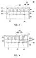
- FIG. 2is a cross-sectional view schematically showing a chip structure according to a first embodiment of the present invention.
- FIG. 3is a cross-sectional view schematically showing a chip structure according to a second embodiment of the present invention.
- FIG. 4is a cross-sectional view schematically showing a chip structure according to a third embodiment of the present invention.
- FIG. 5is a cross-sectional view schematically showing a chip structure according to a forth embodiment of the present invention.
- FIG. 6is a cross-sectional view schematically showing a chip structure according to a fifth embodiment of the present invention.
- FIG. 7is a cross-sectional view schematically showing a chip structure according to a sixth embodiment of the present invention.
- FIG. 8is a cross-sectional view schematically showing a chip structure according to a seventh embodiment of the present invention.
- FIGS. 9-17are various cross-sectional views schematically showing a process of fabricating a chip structure according to an embodiment of the present invention.
- FIG. 17Ais a cross-sectional view schematically showing a chip structure according to another embodiment of the present invention.
- FIG. 17Bis a cross-sectional view schematically showing a chip structure according to another embodiment of the present invention.
- FIG. 17Cis a cross-sectional view schematically showing a chip structure according to another embodiment of the present invention.
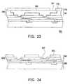
- FIGS. 18-23are various cross-sectional views schematically showing a process of fabricating a chip structure according to another embodiment of the present invention.
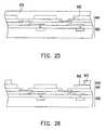
- FIGS. 24-26are various cross-sectional views schematically showing a process of fabricating a dielectric sub-layer according to another embodiment of the present invention.
- ⁇is effect of resistance-capacitance delay
- Ppower loss
- ⁇dielectric constant of dielectric material
- ⁇resistance of traces
- Ltrace length
- Wtrace width
- Spitch between traces
- T u.dthickness of dielectric material
- T mtrace thickness
- tan ⁇dielectric loss
- Vapplied voltage
- ffrequency
- kfactor of capacitor structure.
- the factors of the resistance-capacitance delay and those of the power losscan be known. Therefore, an increase in thickness of every dielectric layer, an application of dielectric material with low dielectric constant, an application of traces with low resistance, or an increase in width or thickness of traces leads an effect of a resistance-capacitance delay and a power loss of a chip to decline.
- FIG. 2a cross-sectional view schematically showing a chip structure according to a first embodiment of the present invention.
- a chip structure 200is provided with a substrate 210 , a first built-up layer 220 , a passivation layer 230 and a second built-up layer 240 .
- the first built-up layer 220is located on the substrate 210 .
- the first built-up layer 220is formed by cross lamination of first metal multi-layers 226 and first dielectric multi-layers.
- plugs 228connect the upper first metal layers 226 with the lower first metal layers 226 or connect the first metal layers 226 with the electric devices 214 .
- the first metal multi-layers 226 and the plugs 228compose a first interconnection scheme 222 .
- the first dielectric multi-layerscompose a first dielectric body 224 .
- the first interconnection scheme 222interlaces inside the first dielectric body 224 and is electrically connected to the electric devices 214 .
- the first interconnection scheme 222includes plenty of conductive pads 227 (only shows one of them) that are exposed outside the first dielectric body 224 .
- the first interconnection scheme 222can electrically connect with other circuits through the conductive pads 227 .
- the first dielectric body 224is made of, for example, an inorganic compound, such as a silicon oxide compound or a silicon nitride compound.
- the material of the first interconnection scheme 222includes, for example, copper, aluminum or tungsten.
- the first metal layers 226 and the plugs 228are made of copper.
- the first interconnection scheme 222is formed by a general process, the first metal layers 226 are made of aluminum and the plugs 228 are made of tungsten.
- the passivation layer 230is disposed on the first built-up layer 220 and is provided with openings exposing the conductive pads 227 .
- the passivation layer 230is contructed of, for example, an inorganic compound, such as a silicon oxide compound, a silicon nitride compound, phosphosilicate glass (PSG), a silicon oxide nitride compound or a composite formed by laminating the above material.
- an inorganic compoundsuch as a silicon oxide compound, a silicon nitride compound, phosphosilicate glass (PSG), a silicon oxide nitride compound or a composite formed by laminating the above material.
- the second built-up layer 240is formed on the passivation layer 230 .
- the second built-up layer 240is formed by cross lamination of second metal multi-layers 246 and second dielectric multi-layers 241 .
- via metal fillers 248connect the upper second metal layers 246 with the lower second metal layers 246 or connect the second metal layers 246 with the conductive pads 227 .
- the second metal layers 246 and the via metal fillers 248compose a second interconnection scheme 242 .
- the second dielectric multi-layers 241compose a second dielectric body 244 .
- the second interconnection scheme 242interlaces inside the second dielectric body 244 and is electrically connected to the conductive pads 227 .
- the second interconnection scheme 242includes plenty of nodes 247 (only shows one of them).
- the second dielectric body 244is provided with openings 249 exposing the nodes 247 of the second interconnection scheme 242 .
- the second interconnection scheme 242can electrically connect with external circuits through the nodes 247 .
- the second dielectric body 244is made of, for example, an organic compound, such as polyimide (PI), benzocyclobutene (BCB), porous dielectric material, parylene, elastomer, or other macromolecule polymers.
- the material of the second interconnection scheme 242includes, for example, copper, aluminum, gold, nickel, titanium-tungsten, titanium or chromium.
- the cross-sectional area A 2 of the traces of the second metal layers 246is extremely larger than the cross-sectional area A 1 of the traces of the first metal layers 226 and than the cross-sectional area of the plugs 228 .
- the cross-sectional area a of the via metal fillers 248is extremely larger than the cross-sectional area A 1 of the traces of the first metal layers 226 and than the cross-sectional area of the plugs 228 .
- the trace width d 2 of the second metal layers 246is extremely larger than the trace width dl of the first metal layers 226 .
- the trace thickness t 2 of the second metal layers 246is extremely larger than the trace thickness t 1 of the first metal layers 226 .
- the thickness L 2 of the individual second dielectric layers 241is extremely larger than the thickness L 1 of the individual first dielectric layers of the first built-up layers 220 .
- the cross-sectional area a of the via metal fillers 248is extremely larger than the area, exposed outside the passivation layer 230 , of the conductive pads 227 .
- the trace width d 2 of the second metal layers 246is larger than 1 micron, and preferably ranges from 1 micron to 1 centimeter.
- the trace thickness t 2 of the second metal layers 246is larger than 1 micron, and preferably ranges from 1 micron to 50 microns.
- the cross-sectional area A 2 of the second metal layers 246is larger than 1 square micron, and preferably ranges from 1 square micron to 0.5 square millimeters.
- the cross-sectional area a of the via metal fillers 248is larger than 1 square micron, and preferably ranges from 1 square micron to 10,000 square microns.
- the thickness L 2 of the individual second dielectric layers 241is larger than 1 micron, and preferably ranges from 1 micron to 100 microns.
- the above chip structurecan decline the resistance-capacitance delay, the power of the chip, and the temperature generated by the driving chip since the cross sectional area, the width and the thickness of the traces of the second metal layers 246 are extremely large, since the cross sectional area of the via metal fillers 248 is also extremely large, since the second interconnection scheme 242 can be made of low-resistance material, such as copper or gold, since the thickness L 2 of the individual second dielectric layers 241 is also extremely large, and since the second dielectric body 244 can be made of organic material, the dielectric constant of which is very low, approximately between 1 ⁇ 3, the practical value depending on the applied organic material.
- the traces of the second interconnection scheme 242are extremely wide and thick and the cross-sectional area of the via metal fillers 248 is extremely large.
- the second interconnection scheme 242can be formed by low-cost fabricating processes, such as an electroplating process, an electroless plating process, or a sputtering process, and, moreover, the second interconnection scheme 242 can be produced using facilities with low accuracy. Therefore, the production costs of the chip structure can be substantially saved.
- the request for the clean room where the second built-up layer is formedis not high, ranging from Class 10 to Class 100. Consequently, the construction cost of the clean room can be conserved.
- the chip structurecan simplify a design of a substrate board due to the layout redistribution, fitting the design of the substrate board, of the nodes 247 of the chip structure by the second interconnection scheme 242 and, besides, the application of the fewer nodes 247 to which ground voltage or power voltage is applied.
- the layout redistribution of nodes 247 of various chips by the second interconnection scheme 242causes the above various chips to be provided with the same node layout
- the node layout, matching the same node layout of the above various chips, of the substrate boardcan be standardized. Therefore, the cost of fabricating the substrate board substantially drops off.
- FIG. 3is a cross-sectional view schematically showing a chip structure according to a second embodiment of the present invention.
- the first interconnection scheme 322 of the built-up layer 320electrically connects the second interconnection scheme 342 of the built-up layer 340 with the electric devices 314 and at least one electrostatic discharge circuit 316 , wherein the electrostatic discharge circuit 316 is disposed on the surface 312 of the substrate 310 .
- the second interconnection scheme 342electrically connects with the power ends of the electric devices 314 .
- the second interconnection scheme 342is designed as a ground bus, the second interconnection scheme 342 electrically connects with the ground ends of the electric devices 314 .
- the second metal layer 346 of the power bus or that of the ground buscan be of, for example, a planer type. According to the above chip structure, each of the power buses or the ground buses can electrically connect with more electric devices 314 than that of prior art. Consequently, the number of the power buses or the ground buses can be reduced and, also, the number of the electrostatic discharge circuits 316 accompanying the power buses or the ground buses can be reduced.
- the number of the nodes 347 accompanying the power buses or the ground busescan be reduced.
- the electrostatic discharge circuits 316can prevent the electric devices 314 electrically connected with the second interconnection scheme 344 from being damaged by the sudden discharge of high voltage.
- the chip structure 300can be electrically connected with external circuits through the nodes 347 applying a flip-chip type, a wire-bonding type or a tape-automated-bonding type.
- FIG. 4is a cross-sectional view schematically showing a chip structure according to a third embodiment of the present invention.
- the first interconnection scheme 422is divided into first interconnections 422 a and first transition interconnections 422 b .
- the second interconnection scheme 442is divided into second interconnections 442 a and second transition interconnections 442 b .
- the nodes 447are electrically connected with the transition devices 418 and the electrostatic discharge circuits 416 through the first transition interconnections 422 b and the second transition interconnections 442 b .
- the transition devices 418are electrically connected with the electric devices 414 through the first interconnections 422 a and the second interconnections 442 a .
- this circuit layoutcan be to transmit clock signals.
- the electrostatic discharge circuits 416can prevent the electric devices 414 and the transition devices 418 from being damaged by the sudden discharge of high voltage.
- the chip structurecan be electrically connected with external circuits through the nodes 447 applying a flip-chip type, a wire-bonding type or a tape-automated-bonding type.
- FIG. 5is a cross-sectional view schematically showing a chip structure according to a forth embodiment of the present invention.
- the second metal layer 1546 of the second interconnection scheme 1542is directly formed on the passivation layer 1530 .
- the second metal layer 1546 of the second interconnection scheme 1542can be directly electrically connected with the conductive pads 1527 , exposed outside the passivation layer 1530 , of the first interconnection scheme 1522 .
- the chip structurecan be electrically connected with external circuits through the nodes 1547 applying a flip-chip type, a wire-bonding type or a tape-automated-bonding type.
- a second built-up layeris constructed from a second dielectric body and a second interconnection scheme.
- a second built-up layeralso can be composed of only a second interconnection scheme, as shown in FIG. 6 .
- FIG. 6is a cross-sectional view schematically showing a chip structure according to a fifth embodiment of the present invention.
- the second metal layer 1646 of the second interconnection schemeis directly formed on the passivation layer 1630 and can be directly electrically connected with the conductive pads 1627 , exposed outside the passivation layer 1630 , of the first interconnection scheme 1622 .
- the second metal layer 1646is exposed to the outside.
- the chip structurecan be electrically connected with external circuits by bonding wires onto the second metal layer 1646 .
- FIG. 7is a cross-sectional view schematically showing a chip structure according to a sixth embodiment of the present invention.
- FIG. 8is a cross-sectional view schematically showing a chip structure according to a seventh embodiment of the present invention.
- the conductive pads 1727 aare exposed to the outside and the conductive pads 1727 b are directly electrically connected with the second metal layer 1746 .
- the chip structure 1700can be electrically connected with external circuits by bonding wires (not shown) onto the conductive pads 1727 a .
- the conductive pads 1727 aare electrically connected with the electrostatic discharge circuits 1716 and the transition devices 1718 respectively.
- the transition devices 1718are electrically connected with the electric devices 1714 .
- bumpsalso can be formed on the conductive pads 1727 a , and the chip structure 1700 can be electrically connected with external circuits through the bumps.
- the conductive pads 827 aare exposed to the outside and the conductive pads 827 b are directly electrically connected with the second interconnection scheme 842 .
- Linking traces 829connect the conductive pads 827 a with the conductive pads 827 b .
- the chip structure 800can be electrically connected with external circuits by bonding wires (not shown) onto the conductive pads 827 a .
- the linking traces 829 and conductive pads 827 bthe conductive pads 827 a are electrically connected with the second interconnection scheme 842 .
- the first interconnection scheme 822the second interconnection scheme 842 is electrically connected with the electric devices 814 .
- bumpsalso can be formed on the conductive pads 827 a , and the chip structure 800 can be electrically connected with external circuits through the bumps.
- the shorter the length S of the linking traces 829the better the electrical efficiency of the chip structure 800 . Otherwise, it is possible that the resistance-capacitance delay and the voltage drop will occur and the chip efficiency will be reduced. It is preferred that the length S of the linking traces 829 is less than 5,000 microns.
- FIGS. 9-17are various cross-sectional views schematically showing a process of fabricating a chip structure according to an embodiment of the present invention.
- a wafer 502is provided with a substrate 510 , a first built-up layer 520 and a passivation layer 530 .
- the first built-up layer 520is formed on the substrate 510 .
- the first built-up layer 520includes a first interconnection scheme 522 and a first dielectric body 524 , wherein the first interconnection scheme 522 interlaces inside the first dielectric body 524 and is electrically connected to the electric devices 514 .
- the first dielectric body 524is constructed from the lamination of first dielectric multi-layers 521 .
- the first interconnection scheme 522includes first metal multi-layers 526 and plugs 528 .
- the first metal layers 526can be electrically connected with the electric devices 514 or the first metal layers 526 neighbored.
- the first interconnection scheme 522further includes one or more conductive pads 527 (only shows one of them) that are exposed outside the first dielectric body 524 .
- the passivation layer 530is formed on the first built-up layer 520 and is provided with one or more openings 532 exposing the conductive pads 527 .
- the largest width of the openings 532ranges from 0.5 to 200 microns for example.
- the openings 532can be formed relatively small, for example, the largest width of the openings 532 ranging from 0.5 to 20 microns, and, correspondingly, the conductive pads 527 can be formed relatively small, the routing density of the top metal layer having the conductive pads 527 can be enhanced. Moreover, due to the design of the openings 532 with relatively small dimensions and high density, correspondingly, the circuits, connecting with the conductive pads 527 , of the second interconnection scheme can be formed small. As a result, the parasitic capacitance generated by the second interconnection scheme can become relatively small.
- a second dielectric sub-layer 541is formed on the passivation layer 530 by, for example, a spin-coating process, wherein the second dielectric sub-layer 541 is made of, for instance, photosensitive organic material.
- one or more via metal openings 543are formed through the second dielectric sub-layer 541 using, for example, a photolithography process.
- the via metal openings 543expose the conductive pads 527 .
- the width of the via metal openings 543can be designed to be larger than that of the openings 532 . This leads conductive metals, during the following metal-filling process, to be easily filled into the via metal openings 543 and the openings 532 .
- the second dielectric sub-layer 541can be made of non-photosensitive organic material such that the via metal openings 543 are formed using a photolithography and etching process.
- the sectional area of the via metal openings 543ranges from 1 square micron to 10,000 square microns.
- a conductive layer 560is formed onto the second dielectric sub-layer 541 , onto the side walls of the via metal openings 543 , and onto the passivation layer 530 and conductive pads 527 exposed by the via metal openings 543 .
- the conductive layer 560is made of, for example, aluminum, titanium-tungsten, titanium or chromium.
- one or more conductive metals 580are deposited on the conductive layer 560 by, for example, an electroplating process or a sputtering process, as shown in FIG. 11 .
- a chemical-mechanical polishing processis preferably used to remove the conductive metals 580 and the conductive layer 560 that are located outside the via metal openings 543 until the second dielectric sub-layer 541 is exposed to the outside, as shown in FIG. 12 .
- another second dielectric sub-layer 570is formed onto the second dielectric sub-layer 541 previously formed.
- a photolithography process or a photolithography and etching processis used to form one or more metal-layer openings 572 through the second dielectric sub-layer 570 , wherein the metal-layer openings 572 expose the conductive metals 580 formed in the via metal openings 542 and the second dielectric sub-layer 541 to the outside.
- another conductive layer 582is formed onto the second dielectric sub-layer 570 , 541 , and onto the side walls of the metal-layer openings 572 , and onto the conductive metals 580 formed in the via metal openings 543 .
- one or more conductive metals 584are deposited on the conductive layer 582 by, for example, an electroplating process or a sputtering process, as shown in FIG. 15 .
- a chemical-mechanical polishing processis preferably used to remove the conductive metals 584 and the conductive layer 582 that are located outside the metal-layer openings 572 until the second dielectric sub-layer 570 is exposed to the outside, as shown in FIG.
- the conductive metals 584 and the conductive layer 582 that are settled in the metal-layer openings 572are defined as a second metal layer 546 .
- the conductive metals 584 and the conductive layer 582 that are settled in the via metal openings 543are defined as via metal fillers 548 .
- the second metal layer 546can be electrically connected with conductive pads 527 through the via metal fillers 548 .
- a wire-bonding processcan be used at this time to form one or more wires electrically connecting the second metal layer 546 with external circuits.
- the other second dielectric sub-layer 590can be selectively formed onto the conductive metals 584 and onto the second dielectric sub-layer 570 .
- the second dielectric sub-layer 590 latest formedcan be a photosensitive material.
- a photolithography processis used to form one or more node openings 592 through the second dielectric sub-layer 590 wherein the node openings 592 expose the conductive metals 584 to the outside.
- the conductive metals 584 exposed to the outsideare defined as nodes 547 .
- the chip structure 500can be electrically connected with external circuits through the nodes 547 .
- the second built-up layer 540is completed so far.
- the second built-up layer 540includes a second interconnection scheme 542 and a second dielectric body 544 , wherein the second interconnection scheme 542 interlaces inside the second dielectric body 544 .
- the second interconnection scheme 542includes at least one second metal layer 546 and at least one via metal filler 548 .
- the via metal filler 548is constructed from the conductive metals 580 and the conductive layer 560 that are disposed in the via metal openings 543 .
- the second metal layer 546is constructed from the conductive metals 580 and the conductive layer 560 that are outside the via metal openings 543 and on the second dielectric sub-layer 541 .
- the via metal filler 548electrically connects the second metal layers 546 with the conductive pads 527 .
- the cross-sectional area of the openings 532is very small, the cross-sectional area of the via metal openings 543 can be designed to be larger than that of the openings 532 .
- the second dielectric body 544is constructed from the lamination of the second dielectric sub-layers 541 , 570 , 590 .
- the structure, material, and dimension of the second built-up layer 540are detailed in the previous embodiments, and the repeat is omitted herein.
- FIG. 17Ais a cross-sectional view schematically showing a chip structure according to another embodiment of the present invention.
- a conductive layer 511 and one or more conductive metals 513are formed into the openings 532 .
- the conductive layer 511is formed onto the passivation layer 530 , the conductive pads 527 and the side walls of the openings 532 using a sputtering process.
- the conductive metals 513are formed onto the conductive layer 511 using a sputtering process or an electroplating process.
- a chemical-mechanical polishing processis preferably used to remove the conductive metals 513 and the conductive layer 511 that are located outside the openings 532 until the passivation layer 520 is exposed to the outside. So far, the conductive metals 513 and the conductive layer 511 are exactly formed into the openings 532 .
- the second dielectric sub-layer 541is formed on the passivation layer 530 by, for example, a spin-coating process and then one or more via metal openings 543 are formed through the second dielectric sub-layer 541 using, for example, a photolithography process.
- the via metal openings 543expose the conductive metals 513 and the conductive layer 511 formed in the openings 532 .
- a conductive layer 560is formed onto the second dielectric sub-layer 541 , onto the side walls of the via metal openings 543 , onto the passivation layer 530 , the conductive metals 513 and the conductive layer 511 that are exposed by the via metal openings 543 .
- the following process of fabricating the second built-up layer 540is detailed in the previous embodiment, and the repeat is omitted herein.
- FIG. 17Bis a cross-sectional view schematically showing a chip structure according to another embodiment of the present invention.
- a conductive layer 682 and conductive metals 684 that are directly formed on the passivation layer 630can be interconnection traces 680 .
- the interconnection traces 680can be formed using a damascene process stated as the above embodiments.
- the second dielectric sub-layer 670 with metal-layer openings 672 in which interconnection traces 680 will be formed during the following processesis formed on the passivation layer 630 .
- a conductive layer 682 and conductive metals 684are sequentially formed into the metal-layer openings 672 and onto the second dielectric sub-layer 670 . Subsequently, the conductive layer 682 and conductive metals 684 outside the metal-layer openings 672 are removed. So far, the formation of the interconnection traces 680 constructed from the conductive layer 682 and the conductive metal 684 are completed.
- a conductive layer 652 and conductive metals 654are formed into the openings 632 of the passivation layer 630 using a damascene process as described in the above embodiment.
- FIGS. 18-23are various cross-sectional views schematically showing a process of fabricating a chip structure according to another embodiment of the present invention.
- a wafer 702is provided.
- the internal structure of the wafer 702is detailed as the previous embodiments, and the repeat is omitted herein.
- a second dielectric sub-layer 741is formed onto the passivation layer 730 of the wafer 702 by, for example, a spin-coating process, wherein the second dielectric sub-layer 741 is made of, for instance, photosensitive material.
- a lithography processis performed.
- a photo mask 790is provided.
- the photo mask 790is divided into at least two regions, a first region 792 and a second region 794 , wherein the energy of the light passing through the first region 792 is stronger than that of the light passing through the second region 794 . Therefore, the first region 792 of the photo mask 790 can be designed as a through-hole type. Light, during an exposing process, can pass through the first region 792 without energy-loss.
- the second region 794 of the photo mask 790can be designed as a type of a semi-transparent membrane.
- the second dielectric sub-layer 741 illuminated by light passing through the first region 792can be exposed absolutely therethrough, while the second dielectric sub-layer 741 illuminated by light passing through the second region 794 can be partially exposed, i.e. not exposed absolutely therethrough. Therefore, after the lithography process is performed, one or more via metal openings 743 and one or more metal-layer openings 745 are formed in the second dielectric sub-layer 741 .
- the via metal openings 743 and the metal-layer openings 745expose conductive pads 727 to the outside.
- the via metal openings 743are formed by light passing through the first region 792 , while the metal-layer openings 745 are formed by light passing through the second region 794 .
- the cross-sectional area of the via metal openings 743can be designed to be larger than that of the openings 732 . This leads conductive metals, during the following metal-filling process, to be easily filled into the via metal openings 743 .
- the cross-sectional area of the via metal fillers 743preferably ranges from 1 square micron to 10,000 square microns.
- a conductive layer 760is formed onto the second dielectric sub-layer 741 , onto the side walls of the via metal openings 743 , onto the side walls of the metal-layer openings 745 , and onto the passivation layer 730 and conductive pads 727 exposed by the via metal openings 743 .
- the conductive layer 760is made of, for example, aluminum, titanium-tungsten, titanium or chromium.
- one or more conductive metals 780are deposited on the conductive layer 582 by, for example, an electroplating process or a sputtering process, as shown in FIG. 21 .
- the material of the conductive metals 780includes copper, nickel, gold or aluminum.
- a chemical-mechanical polishing processis preferably used to remove the conductive metals 780 and the conductive layer 760 that are deposited outside the metal-layer openings 745 and the via metal openings 743 until the second dielectric sub-layer 741 is exposed to the outside, as shown in FIG. 22 .
- the conductive metals 780 and the conductive layer 760 that are settled in the metal-layer openings 745are defined as a second metal layer 746 .
- the conductive metals 780 and the conductive layer 760 that are settled in the via metal openings 743are defined as via metal fillers 748 .
- the second metal layer 746can be electrically connected with conductive pads 727 through the via metal fillers 748 .
- a wire-bonding processcan be used at this time to form one or more wires electrically connecting the second metal layer 746 with external circuits.
- the other second dielectric sub-layer 770can be selectively formed onto the conductive metals 780 and onto the second dielectric sub-layer 741 .
- the second dielectric sub-layer 770 latest formedcan be a photosensitive material.
- a photolithography processis used to form one or more node openings 772 through the second dielectric sub-layer 770 wherein the node openings 772 expose the conductive metals 780 to the outside.
- the conductive metals 780 exposed to the outsideare defined as nodes 747 .
- the chip structure 700can be electrically connected with external circuits through the nodes 747 .
- the structure, material, and dimension of the second built-up layer 740are detailed in the previous embodiments, and the repeat is omitted herein.
- via metal openings and metal-layer openingsare formed by only one photolithography process.
- the application of the present inventionis not limited to the previous embodiments.
- the second dielectric sub-layercan be formed using other processes, described as follows.
- FIGS. 24-26are various cross-sectional views schematically showing a process of fabricating a dielectric sub-layer according to another embodiment of the present invention.
- a second dielectric sub-layer 941is formed onto the passivation layer 930 of the wafer 902 and onto conductive pads 927 using, for example, a spin-coating process, wherein the second dielectric sub-layer 941 is non-photosensitive material.
- via metal openings 943are formed through the second dielectric sub-layer 941 using, for example, a photolithography process and an etching process, wherein the via metal openings 943 expose conductive pads 927 .
- FIG. 24is various cross-sectional views schematically showing a process of fabricating a dielectric sub-layer according to another embodiment of the present invention.
- another second dielectric sub-layer 970is formed onto the second dielectric sub-layer 941 using, for example, a spin-coating process. Further, the second dielectric sub-layer 970 is filled into the via metal openings 943 . The second dielectric sub-layer 970 is photosensitive material. Subsequently, using an exposing process and a developing process, metal-layer openings 972 are formed through the second dielectric sub-layer 970 and the second dielectric sub-layer 970 deposited in the via metal openings 943 is removed, as shown in FIG. 26 .
- the following processincluding a process of forming a conductive layer, a process of forming conductive metals, and a process of removing the conductive layer and the conductive metals deposited outside the metal-layer openings, is similar with the previous embodiment.
- the repeatis omitted herein.
- the etching selectivity between the second dielectric sub-layer 941 and the second dielectric sub-layer 970is requested to be high.
- the etchant of the second dielectric sub-layer 970hardly etches the first dielectric sub-layer 941 . Therefore, after the second dielectric sub-layer 970 is formed onto the second dielectric sub-layer 941 and filled into the via metal openings 943 , a photolithography process and an etching process can be used to form metal-layer openings 972 and to remove the second dielectric sub-layer 970 deposited in the via metal openings 943 .
- the present inventionis not limited to the application of the second metal layer with a signal layer.
- second metal multi-layersalso can be applied in the present invention.
- the fabrication method of the second metal multi-layersis to repeat the above fabrication method of the second metal layer with a single layer.
- the second built-up layer, with second metal multi-layers, fabricated by the above whatever processis finally formed with a second dielectric sub-layer having node openings that expose the second interconnection scheme to be electrically connected with external circuits.
- the whole surface of the second metal layer at the top portioncan be exposed to the outside, and through bumps or conducting wires, the second metal layer can be electrically connected with external circuits.
- the via metal openings of the second dielectric sub-layer at a higher portionexpose the second metal layer at a lower portion so that the conductive metals disposited in the via metal openings electrically connect the upper second metal layer with the lower second metal layer.
- the conductive layer or the conductive metalcan be simultaneously formed into the openings formed through the passivation layer, via metal openings and metal-layer openings, and the configuration constructed from the conductive layer and the conductive metal is shaped with triple layers. Therefore, the process can be called as “triple damascene process”.
- the present inventionhas the following advantages:
- the chip structure of the present inventioncan decline the resistance-capacitance delay, the power of the chip, and the temperature generated by the driving chip since the cross sectional area, the width and the thickness of the traces of the second metal layer are extremely large, since the cross sectional area of the via metal filler is also extremely large, since the second interconnection scheme can be made of low-resistance material, such as copper or gold, since the thickness of the individual second dielectric layer is also extremely large, and since the second dielectric body can be made of organic material, the dielectric constant of which is very low, approximately between 1 ⁇ 3, the practical value depending on the applied organic material.
- each of the power buses or the ground busescan electrically connect with more electric devices than that of prior art. Consequently, the number of the power buses or the ground buses can be reduced and, also, the number of the electrostatic discharge circuits accompanying the power buses or the ground buses can be reduced. In addition, the number of the nodes accompanying the power buses or the ground buses can be reduced.
- the electrostatic discharge circuitscan prevent the electric devices electrically connected with the second interconnection scheme from being damaged by the sudden discharge of high voltage.
- the chip structure of the present inventioncan simplify a design of a substrate board due to the node layout redistribution, fitting the design of the substrate board, of the chip structure by the second interconnection scheme and, besides, the application of the fewer nodes to which ground voltage or power voltage is applied. Moreover, in case the node layout redistribution of various chips by the second interconnection scheme causes the above various chips to be provided with the same node layout, the node layout, matching the same node layout of the above various chips, of the substrate board can be standardized. Therefore, the cost of fabricating the substrate board substantially drops off.
- the second interconnection schemecan be produced using facilities with low accuracy. Therefore, production costs of the chip structure can substantially be reduced.
Landscapes
- Engineering & Computer Science (AREA)
- Physics & Mathematics (AREA)
- Power Engineering (AREA)
- Condensed Matter Physics & Semiconductors (AREA)
- General Physics & Mathematics (AREA)
- Computer Hardware Design (AREA)
- Microelectronics & Electronic Packaging (AREA)
- Manufacturing & Machinery (AREA)
- Geometry (AREA)
- Internal Circuitry In Semiconductor Integrated Circuit Devices (AREA)
- Semiconductor Integrated Circuits (AREA)
- Production Of Multi-Layered Print Wiring Board (AREA)
Abstract
Description
Claims (108)
Priority Applications (1)
| Application Number | Priority Date | Filing Date | Title |
|---|---|---|---|
| US10/337,668US6798073B2 (en) | 2001-12-13 | 2003-01-06 | Chip structure and process for forming the same |
Applications Claiming Priority (11)
| Application Number | Priority Date | Filing Date | Title |
|---|---|---|---|
| TW90130876 | 2001-12-13 | ||
| TW090130876ATW519707B (en) | 2001-12-13 | 2001-12-13 | Chip structure with passivation layer having outer layer connection and its manufacturing process |
| TW90130876A | 2001-12-13 | ||
| TW90131030ATW511243B (en) | 2001-12-14 | 2001-12-14 | Chip structure and process for making the same |
| TW90131030A | 2001-12-14 | ||
| TW90131030 | 2001-12-14 | ||
| TW90131796 | 2001-12-21 | ||
| TW90131796ATW519726B (en) | 2001-12-21 | 2001-12-21 | Chip structure and its process |
| TW90131796A | 2001-12-21 | ||
| US10/125,226US6762115B2 (en) | 1998-12-21 | 2002-04-16 | Chip structure and process for forming the same |
| US10/337,668US6798073B2 (en) | 2001-12-13 | 2003-01-06 | Chip structure and process for forming the same |
Related Parent Applications (1)
| Application Number | Title | Priority Date | Filing Date |
|---|---|---|---|
| US10/125,226DivisionUS6762115B2 (en) | 1998-12-21 | 2002-04-16 | Chip structure and process for forming the same |
Publications (2)
| Publication Number | Publication Date |
|---|---|
| US20030111711A1 US20030111711A1 (en) | 2003-06-19 |
| US6798073B2true US6798073B2 (en) | 2004-09-28 |
Family
ID=27484961
Family Applications (3)
| Application Number | Title | Priority Date | Filing Date |
|---|---|---|---|
| US10/337,668Expired - LifetimeUS6798073B2 (en) | 2001-12-13 | 2003-01-06 | Chip structure and process for forming the same |
| US10/382,699Expired - Fee RelatedUS8211791B2 (en) | 1998-12-21 | 2003-03-05 | Method for fabricating circuitry component |
| US13/277,142Expired - Fee RelatedUS8368204B2 (en) | 1998-12-21 | 2011-10-19 | Chip structure and process for forming the same |
Family Applications After (2)
| Application Number | Title | Priority Date | Filing Date |
|---|---|---|---|
| US10/382,699Expired - Fee RelatedUS8211791B2 (en) | 1998-12-21 | 2003-03-05 | Method for fabricating circuitry component |
| US13/277,142Expired - Fee RelatedUS8368204B2 (en) | 1998-12-21 | 2011-10-19 | Chip structure and process for forming the same |
Country Status (1)
| Country | Link |
|---|---|
| US (3) | US6798073B2 (en) |
Cited By (13)
| Publication number | Priority date | Publication date | Assignee | Title |
|---|---|---|---|---|
| US20040201101A1 (en)* | 2003-04-10 | 2004-10-14 | Kang Seung H. | Aluminum pad power bus and signal routing for integrated circuit devices utilizing copper technology interconnect structures |
| US20050035457A1 (en)* | 2003-08-12 | 2005-02-17 | Renesas Technology Corp. | Interconnecting structure with dummy vias |
| US20050051894A1 (en)* | 2003-09-09 | 2005-03-10 | Intel Corporation | Thick metal layer integrated process flow to improve power delivery and mechanical buffering |
| US20050087844A1 (en)* | 1998-12-21 | 2005-04-28 | Mou-Shiung Lin | Chip structure and process for forming the same |
| US20060012039A1 (en)* | 2003-09-09 | 2006-01-19 | Kim Sarah E | Methods of processing thick ILD layers using spray coating or lamination for C4 wafer level thick metal integrated flow |
| US20070262459A1 (en)* | 1998-12-21 | 2007-11-15 | Mou-Shiung Lin | Top layers of metal for high performance IC's |
| US20080003806A1 (en)* | 2000-10-18 | 2008-01-03 | Megica Corporation | Post passivation interconnection schemes on top of IC chip |
| US7405149B1 (en)* | 1998-12-21 | 2008-07-29 | Megica Corporation | Post passivation method for semiconductor chip or wafer |
| US7482259B2 (en) | 2001-12-13 | 2009-01-27 | Megica Corporation | Chip structure and process for forming the same |
| US20110241216A1 (en)* | 2010-03-31 | 2011-10-06 | Renesas Electronics Corporation | Semiconductor device |
| US8211791B2 (en) | 2001-12-13 | 2012-07-03 | Megica Corporation | Method for fabricating circuitry component |
| US8304907B2 (en) | 1998-12-21 | 2012-11-06 | Megica Corporation | Top layers of metal for integrated circuits |
| US11476220B2 (en) | 2020-03-27 | 2022-10-18 | Samsung Electronics Co., Ltd. | Semiconductor packages |
Families Citing this family (12)
| Publication number | Priority date | Publication date | Assignee | Title |
|---|---|---|---|---|
| US7387960B2 (en)* | 2003-09-16 | 2008-06-17 | Texas Instruments Incorporated | Dual depth trench termination method for improving Cu-based interconnect integrity |
| TWI331370B (en)* | 2004-06-18 | 2010-10-01 | Megica Corp | Connection between two circuitry components |
| US8067837B2 (en) | 2004-09-20 | 2011-11-29 | Megica Corporation | Metallization structure over passivation layer for IC chip |
| US7468545B2 (en)* | 2005-05-06 | 2008-12-23 | Megica Corporation | Post passivation structure for a semiconductor device and packaging process for same |
| US7582556B2 (en)* | 2005-06-24 | 2009-09-01 | Megica Corporation | Circuitry component and method for forming the same |
| CN107923869B (en)* | 2015-08-25 | 2021-10-08 | 生命技术公司 | Design of deep microwell and method of making the same |
| US10352133B2 (en) | 2015-11-04 | 2019-07-16 | Baker Hughes, A Ge Company, Llc | High temperature hydrophobic chemical resistant coating for downhole applications |
| US10681778B2 (en) | 2017-11-21 | 2020-06-09 | Watlow Electric Manufacturing Company | Integrated heater and method of manufacture |
| US10510646B2 (en)* | 2018-02-26 | 2019-12-17 | Taiwan Semiconductor Manufacturing Co., Ltd. | Packae structure, RDL structure and method of forming the same |
| US11967550B2 (en)* | 2020-05-22 | 2024-04-23 | Taiwan Semiconductor Manufacturing Company, Ltd. | Semiconductor structure with via extending across adjacent conductive lines and method of forming the same |
| US11715755B2 (en) | 2020-06-15 | 2023-08-01 | Taiwan Semiconductor Manufacturing Co., Ltd. | Structure and method for forming integrated high density MIM capacitor |
| US11817392B2 (en) | 2020-09-28 | 2023-11-14 | Taiwan Semiconductor Manufacturing Co., Ltd. | Integrated circuit |
Citations (13)
| Publication number | Priority date | Publication date | Assignee | Title |
|---|---|---|---|---|
| US5055907A (en)* | 1989-01-25 | 1991-10-08 | Mosaic, Inc. | Extended integration semiconductor structure with wiring layers |
| US5106461A (en)* | 1989-04-04 | 1992-04-21 | Massachusetts Institute Of Technology | High-density, multi-level interconnects, flex circuits, and tape for tab |
| US5212403A (en)* | 1990-09-10 | 1993-05-18 | Hitachi, Ltd. | Integrated circuit device having an ic chip mounted on the wiring substrate and having suitable mutual connections between internal circuits |
| US5501006A (en)* | 1993-09-22 | 1996-03-26 | Motorola, Inc. | Method for connection of signals to an integrated circuit |
| US5635767A (en)* | 1995-06-02 | 1997-06-03 | Motorola, Inc. | Semiconductor device having built-in high frequency bypass capacitor |
| US5686754A (en)* | 1994-07-12 | 1997-11-11 | International Rectifier Corporation | Polysilicon field ring structure for power IC |
| US5827778A (en)* | 1995-11-28 | 1998-10-27 | Nec Corporation | Method of manufacturing a semiconductor device using a silicon fluoride oxide film |
| US5910020A (en)* | 1995-12-18 | 1999-06-08 | Nec Corporation | Method for fabricating a semiconductor device having a refractory metal pillar for electrical connection |
| US5953626A (en)* | 1996-06-05 | 1999-09-14 | Advanced Micro Devices, Inc. | Dissolvable dielectric method |
| US6100548A (en)* | 1997-04-10 | 2000-08-08 | Hughes Electronics Corporation | Modulation-doped field-effect transistors and fabrication processes |
| US6130457A (en)* | 1996-04-09 | 2000-10-10 | Samsung Electronics Co., Ltd. | Semiconductor-on-insulator devices having insulating layers therein with self-aligned openings |
| US6180426B1 (en)* | 1999-03-01 | 2001-01-30 | Mou-Shiung Lin | High performance sub-system design and assembly |
| US6303423B1 (en)* | 1998-12-21 | 2001-10-16 | Megic Corporation | Method for forming high performance system-on-chip using post passivation process |
Family Cites Families (79)
| Publication number | Priority date | Publication date | Assignee | Title |
|---|---|---|---|---|
| JPS543480A (en) | 1977-06-09 | 1979-01-11 | Fujitsu Ltd | Manufacture of semiconductor device |
| US4267012A (en) | 1979-04-30 | 1981-05-12 | Fairchild Camera & Instrument Corp. | Process for patterning metal connections on a semiconductor structure by using a tungsten-titanium etch resistant layer |
| US4300184A (en)* | 1979-07-11 | 1981-11-10 | Johnson Controls, Inc. | Conformal coating for electrical circuit assemblies |
| US5476211A (en)* | 1993-11-16 | 1995-12-19 | Form Factor, Inc. | Method of manufacturing electrical contacts, using a sacrificial member |
| US5917707A (en)* | 1993-11-16 | 1999-06-29 | Formfactor, Inc. | Flexible contact structure with an electrically conductive shell |
| US5829128A (en)* | 1993-11-16 | 1998-11-03 | Formfactor, Inc. | Method of mounting resilient contact structures to semiconductor devices |
| US4840923A (en)* | 1986-04-30 | 1989-06-20 | International Business Machine Corporation | Simultaneous multiple level interconnection process |
| US4812419A (en) | 1987-04-30 | 1989-03-14 | Hewlett-Packard Company | Via connection with thin resistivity layer |
| JPH01214141A (en)* | 1988-02-23 | 1989-08-28 | Nec Corp | Flip-chip type semiconductor device |
| US5061985A (en)* | 1988-06-13 | 1991-10-29 | Hitachi, Ltd. | Semiconductor integrated circuit device and process for producing the same |
| US5244833A (en)* | 1989-07-26 | 1993-09-14 | International Business Machines Corporation | Method for manufacturing an integrated circuit chip bump electrode using a polymer layer and a photoresist layer |
| US5091289A (en)* | 1990-04-30 | 1992-02-25 | International Business Machines Corporation | Process for forming multi-level coplanar conductor/insulator films employing photosensitive polyimide polymer compositions |
| FR2666190B1 (en)* | 1990-08-24 | 1996-07-12 | Thomson Csf | METHOD AND DEVICE FOR HERMETIC ENCAPSULATION OF ELECTRONIC COMPONENTS. |
| US5266446A (en)* | 1990-11-15 | 1993-11-30 | International Business Machines Corporation | Method of making a multilayer thin film structure |
| SG47403A1 (en) | 1990-12-05 | 1998-04-17 | At & T Corp | Lithographic techniques |
| US5244759A (en) | 1991-02-27 | 1993-09-14 | At&T Bell Laboratories | Single-alignment-level lithographic technique for achieving self-aligned features |
| US5286581A (en) | 1991-08-19 | 1994-02-15 | Motorola, Inc. | Phase-shift mask and method for making |
| US5612254A (en)* | 1992-06-29 | 1997-03-18 | Intel Corporation | Methods of forming an interconnect on a semiconductor substrate |
| KR940001341A (en)* | 1992-06-29 | 1994-01-11 | 디. 아이. 캐플란 | Instant connection for quick electrical access to electronic devices |
| US5371047A (en)* | 1992-10-30 | 1994-12-06 | International Business Machines Corporation | Chip interconnection having a breathable etch stop layer |
| US5407785A (en) | 1992-12-18 | 1995-04-18 | Vlsi Technology, Inc. | Method for generating dense lines on a semiconductor wafer using phase-shifting and multiple exposures |
| JPH06232379A (en)* | 1993-02-01 | 1994-08-19 | Sharp Corp | Solid-state image pickup element |
| US5461333A (en)* | 1993-03-15 | 1995-10-24 | At&T Ipm Corp. | Multi-chip modules having chip-to-chip interconnections with reduced signal voltage level and swing |
| US5641997A (en)* | 1993-09-14 | 1997-06-24 | Kabushiki Kaisha Toshiba | Plastic-encapsulated semiconductor device |
| US6023103A (en)* | 1994-11-15 | 2000-02-08 | Formfactor, Inc. | Chip-scale carrier for semiconductor devices including mounted spring contacts |
| US6835898B2 (en)* | 1993-11-16 | 2004-12-28 | Formfactor, Inc. | Electrical contact structures formed by configuring a flexible wire to have a springable shape and overcoating the wire with at least one layer of a resilient conductive material, methods of mounting the contact structures to electronic components, and applications for employing the contact structures |
| US6577148B1 (en)* | 1994-08-31 | 2003-06-10 | Motorola, Inc. | Apparatus, method, and wafer used for testing integrated circuits formed on a product wafer |
| US5534465A (en)* | 1995-01-10 | 1996-07-09 | At&T Corp. | Method for making multichip circuits using active semiconductor substrates |
| US5731945A (en)* | 1995-02-22 | 1998-03-24 | International Business Machines Corporation | Multichip semiconductor structures with consolidated circuitry and programmable ESD protection for input/output nodes |
| WO1996030933A2 (en)* | 1995-03-20 | 1996-10-03 | Mcnc | Solder bump fabrication methods and structure including a titanium barrier layer |
| US5586121A (en)* | 1995-04-21 | 1996-12-17 | Hybrid Networks, Inc. | Asymmetric hybrid access system and method |
| EP0761721B1 (en) | 1995-08-31 | 2001-02-28 | Infineon Technologies AG | Process for the preparation of poly-o-hydroxyamides and poly-o-mercaptoamides |
| US5818748A (en)* | 1995-11-21 | 1998-10-06 | International Business Machines Corporation | Chip function separation onto separate stacked chips |
| US5960306A (en)* | 1995-12-15 | 1999-09-28 | Motorola, Inc. | Process for forming a semiconductor device |
| US5741624A (en) | 1996-02-13 | 1998-04-21 | Micron Technology, Inc. | Method for reducing photolithographic steps in a semiconductor interconnect process |
| US5686764A (en)* | 1996-03-20 | 1997-11-11 | Lsi Logic Corporation | Flip chip package with reduced number of package layers |
| JP3989038B2 (en)* | 1996-04-17 | 2007-10-10 | 株式会社ルネサステクノロジ | Semiconductor integrated circuit device |
| US5914202A (en) | 1996-06-10 | 1999-06-22 | Sharp Microeletronics Technology, Inc. | Method for forming a multi-level reticle |
| US5985762A (en)* | 1997-05-19 | 1999-11-16 | International Business Machines Corporation | Method of forming a self-aligned copper diffusion barrier in vias |
| US6100184A (en)* | 1997-08-20 | 2000-08-08 | Sematech, Inc. | Method of making a dual damascene interconnect structure using low dielectric constant material for an inter-level dielectric layer |
| US5920790A (en)* | 1997-08-29 | 1999-07-06 | Motorola, Inc. | Method of forming a semiconductor device having dual inlaid structure |
| JP3068534B2 (en)* | 1997-10-14 | 2000-07-24 | 九州日本電気株式会社 | Semiconductor device |
| TW383460B (en) | 1998-02-13 | 2000-03-01 | United Microelectronics Corp | Dual damascene method |
| TW410455B (en)* | 1998-02-16 | 2000-11-01 | United Microelectronics Corp | Forming method for dual damascene structure |
| GB9803771D0 (en)* | 1998-02-23 | 1998-04-15 | Unilever Plc | Soap bar |
| JP3305251B2 (en)* | 1998-02-26 | 2002-07-22 | 松下電器産業株式会社 | Method of forming wiring structure |
| US6075290A (en)* | 1998-02-26 | 2000-06-13 | National Semiconductor Corporation | Surface mount die: wafer level chip-scale package and process for making the same |
| US6207546B1 (en)* | 1998-08-28 | 2001-03-27 | Taiwan Semiconductor Manufacturing Company | Prevent passivation from keyhole damage and resist extrusion by a crosslinking mechanism |
| US6440863B1 (en)* | 1998-09-04 | 2002-08-27 | Taiwan Semiconductor Manufacturing Company | Plasma etch method for forming patterned oxygen containing plasma etchable layer |
| JP2974022B1 (en)* | 1998-10-01 | 1999-11-08 | ヤマハ株式会社 | Bonding pad structure of semiconductor device |
| US6383916B1 (en) | 1998-12-21 | 2002-05-07 | M. S. Lin | Top layers of metal for high performance IC's |
| US6495442B1 (en)* | 2000-10-18 | 2002-12-17 | Magic Corporation | Post passivation interconnection schemes on top of the IC chips |
| US20050032351A1 (en) | 1998-12-21 | 2005-02-10 | Mou-Shiung Lin | Chip structure and process for forming the same |
| US6762115B2 (en) | 1998-12-21 | 2004-07-13 | Megic Corporation | Chip structure and process for forming the same |
| US7405149B1 (en)* | 1998-12-21 | 2008-07-29 | Megica Corporation | Post passivation method for semiconductor chip or wafer |
| US6235628B1 (en)* | 1999-01-05 | 2001-05-22 | Advanced Micro Devices, Inc. | Method of forming dual damascene arrangement for metal interconnection with low k dielectric constant materials and oxide middle etch stop layer |
| TW460991B (en)* | 1999-02-04 | 2001-10-21 | United Microelectronics Corp | Structure of plug that connects the bonding pad |
| US6031293A (en)* | 1999-04-26 | 2000-02-29 | United Microelectronics Corporation | Package-free bonding pad structure |
| US6171732B1 (en) | 1999-05-04 | 2001-01-09 | United Microelectronics Corp. | Method of manufacturing and application of dual alignment photomask |
| US6114233A (en)* | 1999-05-12 | 2000-09-05 | United Microelectronics Corp. | Dual damascene process using low-dielectric constant materials |
| US6306749B1 (en)* | 1999-06-08 | 2001-10-23 | Winbond Electronics Corp | Bond pad with pad edge strengthening structure |
| US6083822A (en)* | 1999-08-12 | 2000-07-04 | Industrial Technology Research Institute | Fabrication process for copper structures |
| US6040243A (en)* | 1999-09-20 | 2000-03-21 | Chartered Semiconductor Manufacturing Ltd. | Method to form copper damascene interconnects using a reverse barrier metal scheme to eliminate copper diffusion |
| US6306769B1 (en) | 2000-01-31 | 2001-10-23 | Advanced Micro Devices | Use of dual patterning masks for printing holes of small dimensions |
| US6399478B2 (en)* | 2000-02-22 | 2002-06-04 | Sanyo Electric Co., Ltd. | Method of making a dual damascene structure with modified insulation |
| AU2001255694A1 (en) | 2000-04-27 | 2001-11-12 | Petersen Advanced Lithography, Inc. | Method for phase shift mask design, fabrication, and use |
| US6578754B1 (en)* | 2000-04-27 | 2003-06-17 | Advanpack Solutions Pte. Ltd. | Pillar connections for semiconductor chips and method of manufacture |
| US6683380B2 (en)* | 2000-07-07 | 2004-01-27 | Texas Instruments Incorporated | Integrated circuit with bonding layer over active circuitry |
| JP3440070B2 (en)* | 2000-07-13 | 2003-08-25 | 沖電気工業株式会社 | Wafer and method of manufacturing wafer |
| US6641982B2 (en) | 2000-12-27 | 2003-11-04 | Intel Corporation | Methodology to introduce metal and via openings |
| US6555479B1 (en) | 2001-06-11 | 2003-04-29 | Advanced Micro Devices, Inc. | Method for forming openings for conductive interconnects |
| US6515369B1 (en)* | 2001-10-03 | 2003-02-04 | Megic Corporation | High performance system-on-chip using post passivation process |
| US6798073B2 (en) | 2001-12-13 | 2004-09-28 | Megic Corporation | Chip structure and process for forming the same |
| TWI280641B (en)* | 2001-12-28 | 2007-05-01 | Via Tech Inc | Chip structure |
| TW557521B (en)* | 2002-01-16 | 2003-10-11 | Via Tech Inc | Integrated circuit package and its manufacturing process |
| KR100892945B1 (en)* | 2002-02-22 | 2009-04-09 | 삼성전자주식회사 | Active matrix organic light emitting display device and manufacturing method thereof |
| US20040137153A1 (en)* | 2002-04-16 | 2004-07-15 | Michael Thomas | Layered stacks and methods of production thereof |
| US6590295B1 (en)* | 2002-06-11 | 2003-07-08 | Taiwan Semiconductor Manufacturing Co., Ltd. | Microelectronic device with a spacer redistribution layer via and method of making the same |
| US6720256B1 (en)* | 2002-12-04 | 2004-04-13 | Taiwan Semiconductor Manufacturing Company | Method of dual damascene patterning |
- 2003
- 2003-01-06USUS10/337,668patent/US6798073B2/ennot_activeExpired - Lifetime
- 2003-03-05USUS10/382,699patent/US8211791B2/ennot_activeExpired - Fee Related
- 2011
- 2011-10-19USUS13/277,142patent/US8368204B2/ennot_activeExpired - Fee Related
Patent Citations (13)
| Publication number | Priority date | Publication date | Assignee | Title |
|---|---|---|---|---|
| US5055907A (en)* | 1989-01-25 | 1991-10-08 | Mosaic, Inc. | Extended integration semiconductor structure with wiring layers |
| US5106461A (en)* | 1989-04-04 | 1992-04-21 | Massachusetts Institute Of Technology | High-density, multi-level interconnects, flex circuits, and tape for tab |
| US5212403A (en)* | 1990-09-10 | 1993-05-18 | Hitachi, Ltd. | Integrated circuit device having an ic chip mounted on the wiring substrate and having suitable mutual connections between internal circuits |
| US5501006A (en)* | 1993-09-22 | 1996-03-26 | Motorola, Inc. | Method for connection of signals to an integrated circuit |
| US5686754A (en)* | 1994-07-12 | 1997-11-11 | International Rectifier Corporation | Polysilicon field ring structure for power IC |
| US5635767A (en)* | 1995-06-02 | 1997-06-03 | Motorola, Inc. | Semiconductor device having built-in high frequency bypass capacitor |
| US5827778A (en)* | 1995-11-28 | 1998-10-27 | Nec Corporation | Method of manufacturing a semiconductor device using a silicon fluoride oxide film |
| US5910020A (en)* | 1995-12-18 | 1999-06-08 | Nec Corporation | Method for fabricating a semiconductor device having a refractory metal pillar for electrical connection |
| US6130457A (en)* | 1996-04-09 | 2000-10-10 | Samsung Electronics Co., Ltd. | Semiconductor-on-insulator devices having insulating layers therein with self-aligned openings |
| US5953626A (en)* | 1996-06-05 | 1999-09-14 | Advanced Micro Devices, Inc. | Dissolvable dielectric method |
| US6100548A (en)* | 1997-04-10 | 2000-08-08 | Hughes Electronics Corporation | Modulation-doped field-effect transistors and fabrication processes |
| US6303423B1 (en)* | 1998-12-21 | 2001-10-16 | Megic Corporation | Method for forming high performance system-on-chip using post passivation process |
| US6180426B1 (en)* | 1999-03-01 | 2001-01-30 | Mou-Shiung Lin | High performance sub-system design and assembly |
Cited By (78)
| Publication number | Priority date | Publication date | Assignee | Title |
|---|---|---|---|---|
| US7482693B2 (en) | 1998-12-21 | 2009-01-27 | Mou-Shiung Lin | Top layers of metal for high performance IC's |
| US8531038B2 (en) | 1998-12-21 | 2013-09-10 | Megica Corporation | Top layers of metal for high performance IC's |
| US8471384B2 (en) | 1998-12-21 | 2013-06-25 | Megica Corporation | Top layers of metal for high performance IC's |
| US20050087844A1 (en)* | 1998-12-21 | 2005-04-28 | Mou-Shiung Lin | Chip structure and process for forming the same |
| US8415800B2 (en) | 1998-12-21 | 2013-04-09 | Megica Corporation | Top layers of metal for high performance IC's |
| US8368204B2 (en) | 1998-12-21 | 2013-02-05 | Megica Corporation | Chip structure and process for forming the same |
| US8350386B2 (en) | 1998-12-21 | 2013-01-08 | Megica Corporation | Top layers of metal for high performance IC's |
| US8304907B2 (en) | 1998-12-21 | 2012-11-06 | Megica Corporation | Top layers of metal for integrated circuits |
| US8022546B2 (en) | 1998-12-21 | 2011-09-20 | Megica Corporation | Top layers of metal for high performance IC's |
| US20070262459A1 (en)* | 1998-12-21 | 2007-11-15 | Mou-Shiung Lin | Top layers of metal for high performance IC's |
| US20070262458A1 (en)* | 1998-12-21 | 2007-11-15 | Mou-Shiung Lin | Top layers of metal for high performance IC's |
| US20070278688A1 (en)* | 1998-12-21 | 2007-12-06 | Mou-Shiung Lin | Top layers of metal for high performance IC's |
| US20070290350A1 (en)* | 1998-12-21 | 2007-12-20 | Mou-Shiung Lin | Top layers of metal for high performance IC's |
| US20070290349A1 (en)* | 1998-12-21 | 2007-12-20 | Mou-Shiung Lin | Top layers of metal for high performance IC's |
| US8022545B2 (en) | 1998-12-21 | 2011-09-20 | Megica Corporation | Top layers of metal for high performance IC's |
| US7999384B2 (en) | 1998-12-21 | 2011-08-16 | Megica Corporation | Top layers of metal for high performance IC's |
| US7915157B2 (en) | 1998-12-21 | 2011-03-29 | Megica Corporation | Chip structure and process for forming the same |
| US7906422B2 (en) | 1998-12-21 | 2011-03-15 | Megica Corporation | Chip structure and process for forming the same |
| US7906849B2 (en) | 1998-12-21 | 2011-03-15 | Megica Corporation | Chip structure and process for forming the same |
| US7884479B2 (en) | 1998-12-21 | 2011-02-08 | Megica Corporation | Top layers of metal for high performance IC's |
| US7863654B2 (en) | 1998-12-21 | 2011-01-04 | Megica Corporation | Top layers of metal for high performance IC's |
| US20080083988A1 (en)* | 1998-12-21 | 2008-04-10 | Mou-Shiung Lin | Top layers of metal for high performance IC's |
| US7358610B2 (en) | 1998-12-21 | 2008-04-15 | Mou-Shiung Lin | Top layers of metal for high performance IC's |
| US7382058B2 (en) | 1998-12-21 | 2008-06-03 | Mou-Shiung Lin | Top layers of metal for high performance IC's |
| US7385292B2 (en) | 1998-12-21 | 2008-06-10 | Mou-Shiung Lin | Top layers of metal for high performance IC's |
| US7385291B2 (en) | 1998-12-21 | 2008-06-10 | Mou-Shiung Lin | Top layers of metal for high performance IC's |
| US7388292B2 (en) | 1998-12-21 | 2008-06-17 | Mou-Shiung Lin | Top layers of metal for high performance IC's |
| US7397135B2 (en) | 1998-12-21 | 2008-07-08 | Mou-Shiung Lin | Top layers of metal for high performance IC's |
| US7396756B2 (en) | 1998-12-21 | 2008-07-08 | Mou-Shiung Lin | Top layers of metal for high performance IC's |
| US7405149B1 (en)* | 1998-12-21 | 2008-07-29 | Megica Corporation | Post passivation method for semiconductor chip or wafer |
| US7425764B2 (en) | 1998-12-21 | 2008-09-16 | Mou-Shiung Lin | Top layers of metal for high performance IC's |
| US20080246154A1 (en)* | 1998-12-21 | 2008-10-09 | Megica Corporation | Top layers of metal for high performance IC's |
| US7442969B2 (en) | 1998-12-21 | 2008-10-28 | Mou-Shiung Lin | Top layers of metal for high performance IC's |
| US7456100B2 (en) | 1998-12-21 | 2008-11-25 | Mou-Shiung Lin | Top layers of metal for high performance IC's |
| US7465975B2 (en) | 1998-12-21 | 2008-12-16 | Mou-Shiung Lin | Top layers of metal for high performance IC's |
| US7470988B2 (en)* | 1998-12-21 | 2008-12-30 | Megica Corporation | Chip structure and process for forming the same |
| US20100117236A1 (en)* | 1998-12-21 | 2010-05-13 | Megica Corporation | Top layers of metal for high performance ic's |
| US20080061444A1 (en)* | 2000-10-18 | 2008-03-13 | Megica Corporation | Post passivation interconnection schemes on top of IC chip |
| US7923366B2 (en) | 2000-10-18 | 2011-04-12 | Megica Corporation | Post passivation interconnection schemes on top of IC chip |
| US8461686B2 (en) | 2000-10-18 | 2013-06-11 | Megica Corporation | Post passivation interconnection schemes on top of IC chip |
| US8482127B2 (en) | 2000-10-18 | 2013-07-09 | Megica Corporation | Post passivation interconnection schemes on top of IC chip |
| US20080067694A1 (en)* | 2000-10-18 | 2008-03-20 | Megica Corporation | Post passivation interconnection schemes on top of IC chip |
| US8492900B2 (en) | 2000-10-18 | 2013-07-23 | Megica Corporation | Post passivation interconnection schemes on top of IC chip |
| US7892965B2 (en) | 2000-10-18 | 2011-02-22 | Megica Corporation | Post passivation interconnection schemes on top of IC chip |
| US7902067B2 (en) | 2000-10-18 | 2011-03-08 | Megica Corporation | Post passivation interconnection schemes on top of the IC chips |
| US20080045002A1 (en)* | 2000-10-18 | 2008-02-21 | Megica Corporation | Post passivation interconnection schemes on top of IC chip |
| US20080045008A1 (en)* | 2000-10-18 | 2008-02-21 | Megica Corporation | Post passivation interconnection schemes on top of IC chip |
| US8188603B2 (en) | 2000-10-18 | 2012-05-29 | Megica Corporation | Post passivation interconnection schemes on top of IC chip |
| US7915161B2 (en)* | 2000-10-18 | 2011-03-29 | Megica Corporation | Post passivation interconnection schemes on top of IC chip |
| US20080042294A1 (en)* | 2000-10-18 | 2008-02-21 | Megica Corporation | Post passivation interconnection schemes on top of IC chip |
| US7919865B2 (en) | 2000-10-18 | 2011-04-05 | Megica Corporation | Post passivation interconnection schemes on top of IC chip |
| US20080003806A1 (en)* | 2000-10-18 | 2008-01-03 | Megica Corporation | Post passivation interconnection schemes on top of IC chip |
| US8435883B2 (en) | 2000-10-18 | 2013-05-07 | Megica Corporation | Post passivation interconnection schemes on top of IC chips |
| US8004088B2 (en) | 2000-10-18 | 2011-08-23 | Megica Corporation | Post passivation interconnection schemes on top of IC chip |
| US20080001300A1 (en)* | 2000-10-18 | 2008-01-03 | Megica Corporation | Post passivation interconnection schemes on top of IC chip |
| US7482259B2 (en) | 2001-12-13 | 2009-01-27 | Megica Corporation | Chip structure and process for forming the same |
| US8008776B2 (en) | 2001-12-13 | 2011-08-30 | Megica Corporation | Chip structure and process for forming the same |
| US7919867B2 (en) | 2001-12-13 | 2011-04-05 | Megica Corporation | Chip structure and process for forming the same |
| US7932603B2 (en) | 2001-12-13 | 2011-04-26 | Megica Corporation | Chip structure and process for forming the same |
| US8546947B2 (en)* | 2001-12-13 | 2013-10-01 | Megica Corporation | Chip structure and process for forming the same |
| US20110278727A1 (en)* | 2001-12-13 | 2011-11-17 | Megica Corporation | Chip structure and process for forming the same |
| US7915734B2 (en) | 2001-12-13 | 2011-03-29 | Megica Corporation | Chip structure and process for forming the same |
| US8211791B2 (en) | 2001-12-13 | 2012-07-03 | Megica Corporation | Method for fabricating circuitry component |
| US7566964B2 (en)* | 2003-04-10 | 2009-07-28 | Agere Systems Inc. | Aluminum pad power bus and signal routing for integrated circuit devices utilizing copper technology interconnect structures |
| US20040201101A1 (en)* | 2003-04-10 | 2004-10-14 | Kang Seung H. | Aluminum pad power bus and signal routing for integrated circuit devices utilizing copper technology interconnect structures |
| US20070007658A1 (en)* | 2003-08-12 | 2007-01-11 | Renesas Technology Corp. | Method of manufacturing interconnecting structure with vias |
| US20050035457A1 (en)* | 2003-08-12 | 2005-02-17 | Renesas Technology Corp. | Interconnecting structure with dummy vias |
| US7605085B2 (en) | 2003-08-12 | 2009-10-20 | Renesas Technology Corp. | Method of manufacturing interconnecting structure with vias |
| US20070190776A1 (en)* | 2003-09-09 | 2007-08-16 | Intel Corporation | Methods of Processing Thick ILD Layers Using Spray Coating or Lamination for C4 Wafer Level Thick Metal Integrated Flow |
| US6977435B2 (en)* | 2003-09-09 | 2005-12-20 | Intel Corporation | Thick metal layer integrated process flow to improve power delivery and mechanical buffering |
| US20050051894A1 (en)* | 2003-09-09 | 2005-03-10 | Intel Corporation | Thick metal layer integrated process flow to improve power delivery and mechanical buffering |
| US20060012039A1 (en)* | 2003-09-09 | 2006-01-19 | Kim Sarah E | Methods of processing thick ILD layers using spray coating or lamination for C4 wafer level thick metal integrated flow |
| US20060076678A1 (en)* | 2003-09-09 | 2006-04-13 | Kim Sarah E | Thick metal layer integrated process flow to improve power delivery and mechanical buffering |
| US8436469B2 (en) | 2010-03-31 | 2013-05-07 | Renesas Electronics Corporation | Semiconductor device |
| US8237287B2 (en)* | 2010-03-31 | 2012-08-07 | Renesas Electronics Corporation | Semiconductor device |
| US20110241216A1 (en)* | 2010-03-31 | 2011-10-06 | Renesas Electronics Corporation | Semiconductor device |
| US8796860B2 (en) | 2010-03-31 | 2014-08-05 | Renesas Electronics Corporation | Semiconductor device |
| US11476220B2 (en) | 2020-03-27 | 2022-10-18 | Samsung Electronics Co., Ltd. | Semiconductor packages |
Also Published As
| Publication number | Publication date |
|---|---|
| US20030111711A1 (en) | 2003-06-19 |
| US8368204B2 (en) | 2013-02-05 |
| US20120098128A1 (en) | 2012-04-26 |
| US20030148604A1 (en) | 2003-08-07 |
| US8211791B2 (en) | 2012-07-03 |
Similar Documents
| Publication | Publication Date | Title |
|---|---|---|
| US8368204B2 (en) | Chip structure and process for forming the same | |
| US6762115B2 (en) | Chip structure and process for forming the same | |
| US6700162B2 (en) | Chip structure to improve resistance-capacitance delay and reduce energy loss of the chip | |
| US7906422B2 (en) | Chip structure and process for forming the same | |
| US8546947B2 (en) | Chip structure and process for forming the same | |
| US7405150B2 (en) | Post passivation interconnection schemes on top of the IC chips | |
| US7381642B2 (en) | Top layers of metal for integrated circuits | |
| US20060267198A1 (en) | High performance integrated circuit device and method of making the same | |
| US20050032351A1 (en) | Chip structure and process for forming the same |
Legal Events
| Date | Code | Title | Description |
|---|---|---|---|
| STCF | Information on status: patent grant | Free format text:PATENTED CASE | |
| AS | Assignment | Owner name:MEGICA CORPORATION, TAIWAN Free format text:ASSIGNMENT OF ASSIGNORS INTEREST;ASSIGNOR:MEGIC CORPORATION;REEL/FRAME:017600/0649 Effective date:20060428 | |
| AS | Assignment | Owner name:MEGIC CORPORATION, TAIWAN Free format text:NUNC PRO TUNC ASSIGNMENT;ASSIGNORS:LIN, MOU-SHIUNG;LEE, JIN-YUAN;HUANG, CHING-CHENG;REEL/FRAME:019026/0349 Effective date:20020131 | |
| FPAY | Fee payment | Year of fee payment:4 | |
| FEPP | Fee payment procedure | Free format text:PAYOR NUMBER ASSIGNED (ORIGINAL EVENT CODE: ASPN); ENTITY STATUS OF PATENT OWNER: LARGE ENTITY | |
| FPAY | Fee payment | Year of fee payment:8 | |
| AS | Assignment | Owner name:MEGIT ACQUISITION CORP., CALIFORNIA Free format text:MERGER;ASSIGNOR:MEGICA CORPORATION;REEL/FRAME:031283/0198 Effective date:20130611 | |
| AS | Assignment | Owner name:QUALCOMM INCORPORATED, CALIFORNIA Free format text:ASSIGNMENT OF ASSIGNORS INTEREST;ASSIGNOR:MEGIT ACQUISITION CORP.;REEL/FRAME:033303/0124 Effective date:20140709 | |
| FPAY | Fee payment | Year of fee payment:12 |