US6798064B1 - Electronic component and method of manufacture - Google Patents
Electronic component and method of manufactureDownload PDFInfo
- Publication number
- US6798064B1 US6798064B1US09/614,794US61479400AUS6798064B1US 6798064 B1US6798064 B1US 6798064B1US 61479400 AUS61479400 AUS 61479400AUS 6798064 B1US6798064 B1US 6798064B1
- Authority
- US
- United States
- Prior art keywords
- layer
- airbridge
- electronic component
- electrically conductive
- substrate
- Prior art date
- Legal status (The legal status is an assumption and is not a legal conclusion. Google has not performed a legal analysis and makes no representation as to the accuracy of the status listed.)
- Expired - Lifetime, expires
Links
Images


Classifications
- H—ELECTRICITY
- H01—ELECTRIC ELEMENTS
- H01L—SEMICONDUCTOR DEVICES NOT COVERED BY CLASS H10
- H01L23/00—Details of semiconductor or other solid state devices
- H01L23/52—Arrangements for conducting electric current within the device in operation from one component to another, i.e. interconnections, e.g. wires, lead frames
- H01L23/522—Arrangements for conducting electric current within the device in operation from one component to another, i.e. interconnections, e.g. wires, lead frames including external interconnections consisting of a multilayer structure of conductive and insulating layers inseparably formed on the semiconductor body
- H01L23/5221—Crossover interconnections
- H—ELECTRICITY
- H01—ELECTRIC ELEMENTS
- H01L—SEMICONDUCTOR DEVICES NOT COVERED BY CLASS H10
- H01L21/00—Processes or apparatus adapted for the manufacture or treatment of semiconductor or solid state devices or of parts thereof
- H01L21/70—Manufacture or treatment of devices consisting of a plurality of solid state components formed in or on a common substrate or of parts thereof; Manufacture of integrated circuit devices or of parts thereof
- H01L21/71—Manufacture of specific parts of devices defined in group H01L21/70
- H01L21/768—Applying interconnections to be used for carrying current between separate components within a device comprising conductors and dielectrics
- H—ELECTRICITY
- H01—ELECTRIC ELEMENTS
- H01L—SEMICONDUCTOR DEVICES NOT COVERED BY CLASS H10
- H01L23/00—Details of semiconductor or other solid state devices
- H01L23/48—Arrangements for conducting electric current to or from the solid state body in operation, e.g. leads, terminal arrangements ; Selection of materials therefor
- H01L23/482—Arrangements for conducting electric current to or from the solid state body in operation, e.g. leads, terminal arrangements ; Selection of materials therefor consisting of lead-in layers inseparably applied to the semiconductor body (electrodes)
- H01L23/4821—Bridge structure with air gap
- H—ELECTRICITY
- H01—ELECTRIC ELEMENTS
- H01L—SEMICONDUCTOR DEVICES NOT COVERED BY CLASS H10
- H01L2924/00—Indexing scheme for arrangements or methods for connecting or disconnecting semiconductor or solid-state bodies as covered by H01L24/00
- H01L2924/0001—Technical content checked by a classifier
- H01L2924/0002—Not covered by any one of groups H01L24/00, H01L24/00 and H01L2224/00
Definitions
- This inventionrelates, in general, to electronics, and more particularly, to electronic components having airbridges and methods of manufacturing electronic components having airbridges.
- Airbridgesare used in electronic components to increase their interconnect speed. Airbridges provide higher interconnect speed because air is used as the interlayer dielectric between adjacent interconnect layers. Air has a lower dielectric constant than conventional interlayer dielectrics such as silicon dioxide and silicon nitride. The lower dielectric constant decreases the parasitic capacitance between adjacent interconnect layers, and the lower parasitic capacitance enables the higher interconnect speed.
- Airbridgesare typically made of gold to provide low electrical resistance, but gold is a soft material.
- the soft, exposed gold of the airbridgesis often damaged during semiconductor wafer processing, assembly, and packaging in an automated manufacturing process.
- the damaged airbridgesreduce the manufacturing yields for the electronic components.
- FIGS. 1 through 8illustrate cross-sectional views of a portion of an electronic component after different manufacturing steps in accordance with an embodiment of the invention.
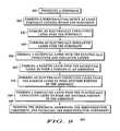
- FIG. 9illustrates a flow chart of a method of manufacturing the electronic component in accordance with an embodiment of the invention.
- FIGS. 1 through 8illustrate cross-sectional views of a portion of an electronic component 100 after different manufacturing steps.
- Electronic component 100comprises a substrate and an airbridge located over the substrate.
- the airbridgehas at least a first layer and a second layer over the first layer.
- the airbridgeis electrically conductive, and the first layer of the airbridge is less resistive than the second layer of the airbridge.
- the second layer of the airbridgecan be electrically conductive or electrically insulative.
- the airbridgeis comprised of three layers: a thin, stiff, electrically conductive barrier layer at the bottom; a thick, soft, electrically conductive layer in the middle; and a thick, hard, electrically insulative, passivating layer at the top.
- the airbridgecan have a design width of approximately 3 to 300 micrometers and a design length of approximately 3 to 30 micrometers. The design length is the distance between landings supporting the airbridge.
- electronic component 100includes a substrate 110 , portions 120 of an electrically conductive layer, and an optional semiconductor device 130 .
- substrate 110is a semiconductor substrate and can include electrically conductive and electrically insulative layers.
- substrate 110can be comprised of a multi-layered Personal Computer Board (PCB).
- PCBPersonal Computer Board
- Optional semiconductor device 130is formed to be located at least partially within or supported by substrate 110 .
- device 130can be a Complementary Metal-Oxide-Semiconductor (CMOS) integrated circuit, a bipolar integrated circuit, or a Bipolar CMOS (BiCMOS) integrated circuit.
- CMOSComplementary Metal-Oxide-Semiconductor
- BiCMOSBipolar CMOS
- an electrically conductive layercan be formed over substrate 110 and device 130 .
- the electrically conductive layercan be an ohmic metal or an interconnect metal.
- an optional insulative layer(not shown in FIG. 1) can be formed over the electrically conductive layer. Holes can be formed in the optional electrically insulative layer to expose portions 120 of the electrically conductive layer. Portions 120 of the electrically conductive layer can be electrically coupled to semiconductor device 130 .
- the electrically conductive layercan be formed after the formation of the optional electrically insulative layer 121 as shown in the resulting structure in FIG. 1 .
- a sacrificial layer 240is formed over a portion of substrate 110 and device 130 .
- sacrificial layer 240can be a positive or negative photoresist material.
- the thickness of sacrificial layer 240is preferably greater than the thickness of a subsequently deposited metal layer.
- the photoresistcan be coated to a thickness of approximately 3.5 micrometers. Next, the photoresist can be soft-baked, and then, the photoresist can be exposed to actinic radiation to define a pattern within the photoresist. Subsequently, the photoresist is developed to produce the profile of sacrificial layer 240 illustrated in FIG. 2 .
- FIG. 3illustrates sacrificial layer 240 after a reflow process and a baking process.
- the photoresistis reflowed to round or smooth the edges of sacrificial layer 240 .
- the rounded or smoothed profile of sacrificial layer 240enables the subsequent formation of a more reliable airbridge.
- This reflow processcan include ramping a reflow temperature from a first temperature up to a second temperature during a first period of time, and heating sacrificial layer 240 from the first temperature up to the second temperature during the first period of time.
- the reflow processcan continue by reflowing sacrificial layer 240 at the second temperature during a second period of time after the first period of time.
- the photoresistcan be heated from approximately 100 degrees Celsius to approximately 130 degrees Celsius within approximately 30 seconds, and then the photoresist can be mediately reflowed at approximately 130 degrees Celsius for approximately 60 seconds.
- this reflow processdoes not use or avoids using Deep Ultra-Violet (DUV) radiation or light.
- DUVDeep Ultra-Violet
- sacrificial layer 240is baked to harden sacrificial layer 240 in its new shape.
- the baking processalso prevents the photoresist of sacrificial layer 240 from undesirably reticulating during a subsequent metal layer deposition.
- This baking processcan include ramping a baking temperature from a third temperature up to a fourth temperature during a third period of time, and heating sacrificial layer 240 from the third temperature up to the fourth temperature during the third period of time.
- the baking processcan continue by baking sacrificial layer 240 at the fourth temperature during a fourth period of time.
- the third temperature of the baking processis equal to the second temperature of the reflow process.
- the photoresistcan be heated from approximately 130 degrees Celsius to approximately 150 degrees Celsius within approximately 30 seconds, and then the photoresist can be immediately baked at approximately 150 degrees Celsius for approximately 180 seconds.
- the baking processdoes not use or avoids using DUV radiation or light.
- a layer 460 and a layer 450 located underneath layer 460are formed over sacrificial layer 240 , substrate 110 , and device 130 to form a portion of an airbridge.
- Layer 450is preferably an electrically conductive barrier layer, and layer 460 is preferably an electrically conductive seed layer. Also in the preferred embodiment, layer 450 is more resistive than layer 460 , and layer 450 is more stiff or rigid than layer 460 .
- layer 450can be sputter deposited to a thickness of approximately 100 to 200 nanometers. In the preferred embodiment, a sputter etch is not performed before sputter depositing layer 450 .
- the thickness of layer 450is preferably at least 100 to 120 nanometers to provide sufficient current flow during a subsequent deplating process. Also in the preferred embodiment, layer 450 has a thickness of approximately 150 nanometers.
- layer 450can be comprised of titanium, titanium tungsten, titanium tungsten nitride, or any combination of such layers.
- Layer 460can be sputter deposited over layer 450 to a thickness of approximately 50 to 200 nanometers. Layer 460 preferably has a thickness of at least 50 to 60 nanometers to provide an adequate seed thickness for a subsequent plating process. As an example, layer 460 can be comprised of gold. In the preferred embodiment, the depositions of layers 450 and 460 are preferably performed below the reflow and bake temperatures described previously for sacrificial layer 240 .
- a plating mask 555is formed over layers 450 and 460 .
- Mask 555exposes a portion of layer 460 to define a plating area.
- Mask 555has a thickness greater than a thickness of the metal layer to be plated.
- mask 555can have a thickness of approximately 3.5 nanometers.
- Mask 555can be formed by coating a layer of photoresist over layers 450 and 460 , soft-baking the photoresist, exposing the photoresist to a pattern of actinic radiation, and developing the photoresist. In the preferred embodiment, mask 555 is not exposed to DUV radiation or light.
- mask 555is preferably not exposed to a baking process between the exposure and developing steps, and mask 555 is also preferably not exposed to a hard-bake or curing process after the developing step. After forming mask 555 , the exposed portion of layer 460 is cleaned.
- an electrically conductive layer 660is plated over layer 450 .
- layer 660can be plated to a thickness of approximately 2.6 micrometers. The plating of layer 660 forms another portion of the airbridge.
- Layer 660preferably has a width greater than the design width described earlier.
- Layer 660includes layer 460 of FIG. 5 . Accordingly, layer 660 in FIG. 6 is comprised of the same material as layer 460 of FIG. 5 .
- the etching of layer 450is preferably performed using a timed etch and not an endpointed etch because of the difficulties of detecting the etch endpoint. Also in the preferred embodiment, the etching of layer 450 is performed using a dry etching process and not a wet etching process to minimize the undercutting of layer 450 .
- the sacrificial layeris removed to form a gap 770 underneath layers 660 and 450 and between layer 450 and substrate 110 .
- the sacrificial layercan be removed using a Kwik Strip chemical, commercially available from AZ Clariant of Sunnyvale, Calif.
- the sacrificial layercan be removed by being soaked in the Kwik Strip chemical for approximately 30 minutes at a temperature of approximately 90 degrees Celsius.
- acetonecan be used to remove the sacrificial layer.
- the sacrificial layeris removed after plating layer 660 and before forming a subsequent portion of the airbridge.
- electronic component 100is illustrated to include a layer 880 , which forms another portion of the airbridge.
- the airbridgeis identified by element number 890 in FIG. 8 .
- layer 880is a passivation layer that prevents scratches and other defects in the underlying, softer layer 660 during subsequent processing, assembly, packaging, and handling of electronic component 100 . Accordingly, layer 880 is harder than layer 660 . Layer 880 also strengthens the airbridge. Accordingly, layer 880 is stiffer than layer 660 .
- layer 880can be comprised of an electrically insulative material such as polyimide, silicon dioxide, silicon nitride, silicon oxy-nitride, or Tetra-Ethyl-Ortho-Silicate (TEOS). Accordingly, layer 880 is preferably more resistive than layers 450 and 660 . In an alternative embodiment, layer 880 can be electrically conductive.
- an electrically insulative materialsuch as polyimide, silicon dioxide, silicon nitride, silicon oxy-nitride, or Tetra-Ethyl-Ortho-Silicate (TEOS). Accordingly, layer 880 is preferably more resistive than layers 450 and 660 . In an alternative embodiment, layer 880 can be electrically conductive.
- Layer 880has a thickness that is less than a combined thickness of layers 450 and 460 and gap 770 .
- the thickness of gap 770is the height of gap 770 or the distance between layer 450 and the top surface of substrate 110 in FIG. 8 .
- layer 880has a thickness that is less than approximately fifty percent of the combined thickness of layers 450 and 660 and gap 770 or the combined thickness of only layer 660 and gap 770 .
- layer 880can have a thickness of approximately 800 nanometers. The small thickness of layer 880 prevents layer 880 from sealing gap 770 . In the preferred embodiment, gap 770 is not even partially sealed by layer 880 .
- Layer 880is preferably deposited using a Chemical Vapor Deposition (CVD) process operated at a low temperature, below approximately 350 degrees Celsius, and at a reduced pressure, below approximately 1.5 Torr. These deposition parameters give layer 880 a fairly low compressive stress level of approximately 0 to 200 MegaPascals (MPa), which strengthens the airbridge. On average, layer 800 has a compressive stress level of approximately 100 MPa.
- CVDChemical Vapor Deposition
- the CVD processalso preferably deposits layer 880 in a substantially vertical and substantially conformal manner.
- the vertical nature of the depositionprevents layer 880 from being formed under a center or central portion of the width of the airbridge where the central portion of the width of the airbridge forms the aforementioned design width of the airbridge. Therefore, in the preferred embodiment, the design width portion of the airbridge does not overlap any of the portion of layer 880 located underneath the airbridge.
- portions of layer 880may be located underneath peripheral edges of the airbridge, but a significant portion of the airbridge preferably does not overlap the portion of layer 880 located underneath the airbridge. As an example, an overlap of approximately 3% to 10% of the actual airbridge width can overlap the portions of layer 880 located underneath the airbridge.
- an etch mask(not shown in FIG. 8) is formed over layer 880 .
- the etch maskis comprised of positive, not negative, photoresist to directly protect portions of layer 880 , the sides of layers 660 and 450 , and the portion of the top surface of substrate 110 located underneath the airbridge.
- the etch maskcan have a thickness of approximately 3.5 micrometers.
- the photoresist of the etch maskcan be coated over layer 880 , soft-baked using a ramped baking temperature, exposed to a pattern of actinic radiation, and developed.
- the photoresistis not exposed to DUV radiation or light and is also not baked or cured after being exposed or developed.
- the soft-bake processoccurs over a range of temperatures in ambient or a higher pressure.
- the photoresistcan be heated over a range of temperatures during a fifth time period.
- electronic component 100can be lowered to approximately 1 millimeter above a heating surface that is heated to a temperature of approximately 120 degrees Celsius. Then, over approximately 90 seconds, electronic component 100 can be lowered at a linear rate to contact the heating surface. Immediately afterwards, electronic component 100 can be baked for approximately 5 seconds while contacting the heating surface, which remains heated to 120 degrees Celsius.
- the exposed portions of layer 880are etched to expose underlying bond pads.
- the etch maskis removed, and substrate 110 can be thinned.
- the thinning processcan include mounting electronic component 100 upside down on a support wafer comprised of sapphire, mechanically grinding the back surface of substrate 110 , wet and dry etching the back surface of substrate 110 , and demounting electronic component 100 from the support wafer.
- substrate 110can be sawn to singulate electronic component 100 from other electronic components formed in or over substrate 110 .
- electronic component 100can be picked and placed onto a lead frame for assembly and packaging.
- gap 770 underneath the airbridgecan be filled with air or another gas.
- FIG. 9illustrates a flow chart of the method of manufacturing electronic component 100 described previously with reference to FIGS. 1 through 8.
- a substrateis provided, and at a step 920 of method 900 , a semiconductor device is formed at least partially located within the substrate.
- an electrically conductive layeris formed over the substrate, and at a step 940 , an electrically insulative layer is formed over the substrate.
- a sacrificial layeris formed over the electrically insulative and conductive layers.
- step 950includes the ramped temperature reflow and baking processes described earlier.
- step 960 of method 900an electrically conductive barrier layer is formed over the sacrificial layer to form a portion of an airbridge.
- step 960includes the sputter deposition and subsequent patterning of the barrier layer.
- step 970 of method 900an electrically conductive layer is formed over the barrier layer to form another portion of the airbridge.
- step 970includes the sputter deposition of a seed layer, the plating of the plated layer, and the subsequent patterning or deplating of the seed layer.
- a passivation layeris formed over the electrically conductive layer to form yet another portion of the airbridge.
- step 980includes the deposition of the passivation layer and the subsequent patterning of the passivation layer.
- the patterning of the passivation layerincludes the ramped temperature soft-baking of the photoresist used to define the pattern in the passivation layer.
- the substrateis thinned, assembled, and packaged into a semiconductor or electronic component.
- the method of manufacturing electronic component 100 described in FIGS. 1 through 8provides many non-obvious advantages.
- layer 880(FIG. 8) as part of the airbridge protects the airbridge during the processing steps occurring after formation of the airbridge.
- layer 880preferably has a low stress level to minimize any problems associated with a mismatch between the coefficients of thermal expansion between layers 660 and 880 (FIG. 8 ).
- layer 880is preferably not located underneath a substantial portion of the airbridge to minimize the parasitic capacitance between the airbridge and underlying interconnect layers.
- the ramped temperature for the soft-baking of the etch mask over layer 880improves the manufacturing yield for electronic component 100 .
- the elimination of the post-exposure bake and the post-develop bake for the etch mask located over layer 880also improves the manufacturing yield for electronic component 100 .
- the electrical testing of the electronic component described hereinhas demonstrated the reliability and robustness of the airbridges.
Landscapes
- Engineering & Computer Science (AREA)
- Physics & Mathematics (AREA)
- Condensed Matter Physics & Semiconductors (AREA)
- General Physics & Mathematics (AREA)
- Computer Hardware Design (AREA)
- Microelectronics & Electronic Packaging (AREA)
- Power Engineering (AREA)
- Manufacturing & Machinery (AREA)
- Internal Circuitry In Semiconductor Integrated Circuit Devices (AREA)
Abstract
Description
Claims (16)
Priority Applications (7)
| Application Number | Priority Date | Filing Date | Title |
|---|---|---|---|
| US09/614,794US6798064B1 (en) | 2000-07-12 | 2000-07-12 | Electronic component and method of manufacture |
| CNB018140610ACN100492625C (en) | 2000-07-12 | 2001-07-11 | Electronic component and method for manufacturing the same |
| EP01961635AEP1303879A2 (en) | 2000-07-12 | 2001-07-11 | Electronic component and method of manufacture |
| JP2002509106AJP2004514271A (en) | 2000-07-12 | 2001-07-11 | Electronic components and manufacturing method |
| KR1020037000485AKR100779869B1 (en) | 2000-07-12 | 2001-07-11 | Electronic component and manufacturing method |
| AU2001282884AAU2001282884A1 (en) | 2000-07-12 | 2001-07-11 | Electronic component and method of manufacture |
| PCT/US2001/022014WO2002005347A2 (en) | 2000-07-12 | 2001-07-11 | Electronic component and method of manufacture |
Applications Claiming Priority (1)
| Application Number | Priority Date | Filing Date | Title |
|---|---|---|---|
| US09/614,794US6798064B1 (en) | 2000-07-12 | 2000-07-12 | Electronic component and method of manufacture |
Publications (1)
| Publication Number | Publication Date |
|---|---|
| US6798064B1true US6798064B1 (en) | 2004-09-28 |
Family
ID=24462716
Family Applications (1)
| Application Number | Title | Priority Date | Filing Date |
|---|---|---|---|
| US09/614,794Expired - LifetimeUS6798064B1 (en) | 2000-07-12 | 2000-07-12 | Electronic component and method of manufacture |
Country Status (7)
| Country | Link |
|---|---|
| US (1) | US6798064B1 (en) |
| EP (1) | EP1303879A2 (en) |
| JP (1) | JP2004514271A (en) |
| KR (1) | KR100779869B1 (en) |
| CN (1) | CN100492625C (en) |
| AU (1) | AU2001282884A1 (en) |
| WO (1) | WO2002005347A2 (en) |
Cited By (10)
| Publication number | Priority date | Publication date | Assignee | Title |
|---|---|---|---|---|
| US20060061887A1 (en)* | 2004-09-17 | 2006-03-23 | Toshiba Samsung Storage Technology Korea Corporation | Optical pickup actuator and method with multi-conductive suspension |
| US20060199322A1 (en)* | 2005-03-02 | 2006-09-07 | Mitsubishi Denki Kabushiki Kaisha | Method of manufacturing semiconductor device including air space formed around gate electrode |
| US20070123026A1 (en)* | 2005-11-28 | 2007-05-31 | Mitsubishi Electric Corporation | Semiconductor device having high frequency components and manufacturing method thereof |
| US20100046079A1 (en)* | 2004-02-12 | 2010-02-25 | Jun-Bo Yoon | Polymer pattern and metal film pattern, metal pattern, plastic mold using thereof, and method of the forming the same |
| US20100238638A1 (en)* | 2009-03-19 | 2010-09-23 | Samsung Electronics Co., Ltd. | Semiconductor package |
| US8603846B2 (en) | 2004-07-12 | 2013-12-10 | International Business Machines Corporation | Processing for overcoming extreme topography |
| US9543262B1 (en) | 2009-08-18 | 2017-01-10 | Cypress Semiconductor Corporation | Self aligned bump passivation |
| US9859205B2 (en)* | 2011-01-31 | 2018-01-02 | Avago Technologies General Ip (Singapore) Pte. Ltd. | Semiconductor device having an airbridge and method of fabricating the same |
| US10132712B1 (en) | 2016-09-14 | 2018-11-20 | Northrop Grumman Systems Corporation | Micro hermetic sensor |
| CN110491830A (en)* | 2019-07-18 | 2019-11-22 | 福建省福联集成电路有限公司 | A kind of method for producing air bridge and the device with the air bridges |
Families Citing this family (9)
| Publication number | Priority date | Publication date | Assignee | Title |
|---|---|---|---|---|
| JP4599342B2 (en) | 2005-12-27 | 2010-12-15 | エーエスエムエル ネザーランズ ビー.ブイ. | Optical apparatus, lithographic apparatus, and device manufacturing method |
| US7767589B2 (en) | 2007-02-07 | 2010-08-03 | Raytheon Company | Passivation layer for a circuit device and method of manufacture |
| JP5369544B2 (en)* | 2008-08-29 | 2013-12-18 | 富士通株式会社 | Semiconductor device and manufacturing method thereof |
| KR101043343B1 (en)* | 2008-12-30 | 2011-06-21 | (재)나노소자특화팹센터 | Air bridge manufacturing method using negative photoresist |
| WO2010116819A1 (en)* | 2009-04-07 | 2010-10-14 | 株式会社村田製作所 | Manufacturing method for electronic components |
| CN102832162A (en)* | 2011-06-13 | 2012-12-19 | 中芯国际集成电路制造(上海)有限公司 | Air bridge three-dimensional circuit and manufacturing method thereof |
| JP5909980B2 (en) | 2011-10-12 | 2016-04-27 | 三菱電機株式会社 | Semiconductor device and manufacturing method thereof |
| CN110277376B (en)* | 2019-05-07 | 2020-12-11 | 福建省福联集成电路有限公司 | Air bridge integrated inductor and manufacturing method thereof |
| CN113764261B (en)* | 2020-10-15 | 2023-08-22 | 腾讯科技(深圳)有限公司 | Hollow bridge structure and manufacturing method thereof, superconducting quantum chip and manufacturing method thereof |
Citations (13)
| Publication number | Priority date | Publication date | Assignee | Title |
|---|---|---|---|---|
| US4857481A (en) | 1989-03-14 | 1989-08-15 | Motorola, Inc. | Method of fabricating airbridge metal interconnects |
| JPH01245530A (en) | 1988-03-28 | 1989-09-29 | Rohm Co Ltd | Method of packaging semiconductor device |
| JPH01262646A (en) | 1988-04-14 | 1989-10-19 | Sharp Corp | Semiconductor device |
| US4916520A (en) | 1987-09-24 | 1990-04-10 | Nec Corporation | Semiconductor device with airbridge interconnection |
| EP0501407A1 (en) | 1991-02-25 | 1992-09-02 | Kabushiki Kaisha Toshiba | Semiconductor integrated circuit having wirings |
| US5219713A (en) | 1990-12-17 | 1993-06-15 | Rockwell International Corporation | Multi-layer photoresist air bridge fabrication method |
| US5408742A (en) | 1991-10-28 | 1995-04-25 | Martin Marietta Corporation | Process for making air bridges for integrated circuits |
| EP0693778A2 (en) | 1994-07-20 | 1996-01-24 | Mitsubishi Denki Kabushiki Kaisha | Semiconductor device with integral heatsink |
| US5677574A (en) | 1995-04-12 | 1997-10-14 | Mitsubishi Denki Kabushiki Kaisha | Airbridge wiring structure for MMIC |
| US5686743A (en) | 1996-07-10 | 1997-11-11 | Trw Inc. | Method of forming airbridged metallization for integrated circuit fabrication |
| US6037245A (en) | 1998-06-30 | 2000-03-14 | Fujitsu Quantum Devices Limited | High-speed semiconductor device having a dual-layer gate structure and a fabrication process thereof |
| US6268262B1 (en)* | 1995-10-23 | 2001-07-31 | Dow Corning Corporation | Method for forming air bridges |
| US6380552B2 (en)* | 1999-05-28 | 2002-04-30 | Hrl Laboratories, Llc | Low turn-on voltage InP Schottky device and method |
Family Cites Families (10)
| Publication number | Priority date | Publication date | Assignee | Title |
|---|---|---|---|---|
| JPH01166541A (en)* | 1987-12-23 | 1989-06-30 | Hitachi Ltd | Semiconductor device and manufacture thereof |
| JPH02170554A (en)* | 1988-12-23 | 1990-07-02 | Sumitomo Electric Ind Ltd | Semiconductor device and its manufacturing method |
| JP2837036B2 (en)* | 1992-07-31 | 1998-12-14 | シャープ株式会社 | Method of forming gate electrode |
| JPH0689940A (en)* | 1992-09-08 | 1994-03-29 | Mitsubishi Electric Corp | Air bridge wiring structure |
| JP3455995B2 (en)* | 1993-11-11 | 2003-10-14 | 株式会社デンソー | Air bridge wiring for high frequency circuit devices |
| EP0775931B1 (en)* | 1995-11-21 | 2005-10-05 | Samsung Electronics Co., Ltd. | Method of manufacturing a liquid crystal display |
| US6492705B1 (en)* | 1996-06-04 | 2002-12-10 | Intersil Corporation | Integrated circuit air bridge structures and methods of fabricating same |
| JPH1012722A (en)* | 1996-06-26 | 1998-01-16 | Mitsubishi Electric Corp | Semiconductor device |
| JP3674209B2 (en)* | 1997-01-23 | 2005-07-20 | ソニー株式会社 | Solid-state imaging device and manufacturing method thereof |
| JP4221788B2 (en)* | 1997-11-17 | 2009-02-12 | 住友化学株式会社 | Method for forming resist pattern with excellent heat resistance and positive resist composition used therefor |
- 2000
- 2000-07-12USUS09/614,794patent/US6798064B1/ennot_activeExpired - Lifetime
- 2001
- 2001-07-11WOPCT/US2001/022014patent/WO2002005347A2/ennot_activeApplication Discontinuation
- 2001-07-11JPJP2002509106Apatent/JP2004514271A/enactivePending
- 2001-07-11CNCNB018140610Apatent/CN100492625C/ennot_activeExpired - Fee Related
- 2001-07-11KRKR1020037000485Apatent/KR100779869B1/ennot_activeExpired - Fee Related
- 2001-07-11AUAU2001282884Apatent/AU2001282884A1/ennot_activeAbandoned
- 2001-07-11EPEP01961635Apatent/EP1303879A2/ennot_activeWithdrawn
Patent Citations (14)
| Publication number | Priority date | Publication date | Assignee | Title |
|---|---|---|---|---|
| US4916520A (en) | 1987-09-24 | 1990-04-10 | Nec Corporation | Semiconductor device with airbridge interconnection |
| JPH01245530A (en) | 1988-03-28 | 1989-09-29 | Rohm Co Ltd | Method of packaging semiconductor device |
| JPH01262646A (en) | 1988-04-14 | 1989-10-19 | Sharp Corp | Semiconductor device |
| US4857481A (en) | 1989-03-14 | 1989-08-15 | Motorola, Inc. | Method of fabricating airbridge metal interconnects |
| US5219713A (en) | 1990-12-17 | 1993-06-15 | Rockwell International Corporation | Multi-layer photoresist air bridge fabrication method |
| EP0501407A1 (en) | 1991-02-25 | 1992-09-02 | Kabushiki Kaisha Toshiba | Semiconductor integrated circuit having wirings |
| US5408742A (en) | 1991-10-28 | 1995-04-25 | Martin Marietta Corporation | Process for making air bridges for integrated circuits |
| EP0693778A2 (en) | 1994-07-20 | 1996-01-24 | Mitsubishi Denki Kabushiki Kaisha | Semiconductor device with integral heatsink |
| US5677574A (en) | 1995-04-12 | 1997-10-14 | Mitsubishi Denki Kabushiki Kaisha | Airbridge wiring structure for MMIC |
| US6268262B1 (en)* | 1995-10-23 | 2001-07-31 | Dow Corning Corporation | Method for forming air bridges |
| US5686743A (en) | 1996-07-10 | 1997-11-11 | Trw Inc. | Method of forming airbridged metallization for integrated circuit fabrication |
| US5817446A (en) | 1996-07-10 | 1998-10-06 | Trw Inc. | Method of forming airbridged metallization for integrated circuit fabrication |
| US6037245A (en) | 1998-06-30 | 2000-03-14 | Fujitsu Quantum Devices Limited | High-speed semiconductor device having a dual-layer gate structure and a fabrication process thereof |
| US6380552B2 (en)* | 1999-05-28 | 2002-04-30 | Hrl Laboratories, Llc | Low turn-on voltage InP Schottky device and method |
Cited By (15)
| Publication number | Priority date | Publication date | Assignee | Title |
|---|---|---|---|---|
| US20100046079A1 (en)* | 2004-02-12 | 2010-02-25 | Jun-Bo Yoon | Polymer pattern and metal film pattern, metal pattern, plastic mold using thereof, and method of the forming the same |
| US8603846B2 (en) | 2004-07-12 | 2013-12-10 | International Business Machines Corporation | Processing for overcoming extreme topography |
| US9263292B2 (en) | 2004-07-12 | 2016-02-16 | Globalfoundries Inc. | Processing for overcoming extreme topography |
| US7478411B2 (en) | 2004-09-17 | 2009-01-13 | Toshiba Samsung Storage Technology Korea Corporation | Optical pickup actuator and method with multi-conductive suspension |
| US20060061887A1 (en)* | 2004-09-17 | 2006-03-23 | Toshiba Samsung Storage Technology Korea Corporation | Optical pickup actuator and method with multi-conductive suspension |
| US20060199322A1 (en)* | 2005-03-02 | 2006-09-07 | Mitsubishi Denki Kabushiki Kaisha | Method of manufacturing semiconductor device including air space formed around gate electrode |
| US7358179B2 (en)* | 2005-03-02 | 2008-04-15 | Mitsubishi Denki Kabushiki Kaisha | Method of manufacturing semiconductor device including air space formed around gate electrode |
| US7768043B2 (en)* | 2005-11-28 | 2010-08-03 | Mitsubishi Electric Corporation | Semiconductor device having high frequency components and manufacturing method thereof |
| US20070123026A1 (en)* | 2005-11-28 | 2007-05-31 | Mitsubishi Electric Corporation | Semiconductor device having high frequency components and manufacturing method thereof |
| US20100238638A1 (en)* | 2009-03-19 | 2010-09-23 | Samsung Electronics Co., Ltd. | Semiconductor package |
| US8692133B2 (en)* | 2009-03-19 | 2014-04-08 | Samsung Electronics Co., Ltd. | Semiconductor package |
| US9543262B1 (en) | 2009-08-18 | 2017-01-10 | Cypress Semiconductor Corporation | Self aligned bump passivation |
| US9859205B2 (en)* | 2011-01-31 | 2018-01-02 | Avago Technologies General Ip (Singapore) Pte. Ltd. | Semiconductor device having an airbridge and method of fabricating the same |
| US10132712B1 (en) | 2016-09-14 | 2018-11-20 | Northrop Grumman Systems Corporation | Micro hermetic sensor |
| CN110491830A (en)* | 2019-07-18 | 2019-11-22 | 福建省福联集成电路有限公司 | A kind of method for producing air bridge and the device with the air bridges |
Also Published As
| Publication number | Publication date |
|---|---|
| KR100779869B1 (en) | 2007-11-27 |
| JP2004514271A (en) | 2004-05-13 |
| KR20030020930A (en) | 2003-03-10 |
| AU2001282884A1 (en) | 2002-01-21 |
| CN100492625C (en) | 2009-05-27 |
| WO2002005347A3 (en) | 2002-04-25 |
| WO2002005347A2 (en) | 2002-01-17 |
| CN1446377A (en) | 2003-10-01 |
| EP1303879A2 (en) | 2003-04-23 |
Similar Documents
| Publication | Publication Date | Title |
|---|---|---|
| US6798064B1 (en) | Electronic component and method of manufacture | |
| US7892972B2 (en) | Methods for fabricating and filling conductive vias and conductive vias so formed | |
| US4827326A (en) | Integrated circuit having polyimide/metal passivation layer and method of manufacture using metal lift-off | |
| JP5474534B2 (en) | Passivation and contact surrounded by polyimide and method of manufacturing the same | |
| JP2785338B2 (en) | Method for manufacturing semiconductor device | |
| JP3538029B2 (en) | Method for manufacturing semiconductor device | |
| US6639314B2 (en) | Solder bump structure and a method of forming the same | |
| US20030171001A1 (en) | Method of manufacturing semiconductor devices | |
| US20050077626A1 (en) | Forming of the last metallization level of an integrated circuit | |
| JPH0669351A (en) | Manufacture of contact of multilayer metal interconnection structure | |
| US6228753B1 (en) | Method of fabricating a bonding pad structure for improving the bonding pad surface quality | |
| US6878642B1 (en) | Method to improve passivation openings by reflow of photoresist to eliminate tape residue | |
| US20060183312A1 (en) | Method of forming chip-type low-k dielectric layer | |
| JPH0661233A (en) | Manufacture of semiconductor device | |
| JPH10223759A (en) | Method for forming multilayer wiring of semiconductor device | |
| KR100620911B1 (en) | Gold bump manufacturing method of semiconductor device | |
| JPS6336548A (en) | Semiconductor device and manufacture thereof | |
| JP2739842B2 (en) | Method for manufacturing semiconductor device | |
| US20240071762A1 (en) | Integrated circuit having an improved metal layer | |
| JP3166912B2 (en) | Method for manufacturing semiconductor device | |
| JP2991388B2 (en) | Method for manufacturing semiconductor device | |
| JPH06104315A (en) | Semiconductor package and manufacturing method thereof | |
| KR100275949B1 (en) | A method of fabricating semiconductor device | |
| JPH05114537A (en) | Manufacture of semiconductor integrated circuit | |
| KR20080047666A (en) | Method for manufacturing a semiconductor device having a fuse |
Legal Events
| Date | Code | Title | Description |
|---|---|---|---|
| AS | Assignment | Owner name:FREESCALE SEMICONDUCTOR, INC., TEXAS Free format text:ASSIGNMENT OF ASSIGNORS INTEREST;ASSIGNOR:MOTOROLA, INC;REEL/FRAME:015360/0718 Effective date:20040404 Owner name:FREESCALE SEMICONDUCTOR, INC.,TEXAS Free format text:ASSIGNMENT OF ASSIGNORS INTEREST;ASSIGNOR:MOTOROLA, INC;REEL/FRAME:015360/0718 Effective date:20040404 | |
| STCF | Information on status: patent grant | Free format text:PATENTED CASE | |
| AS | Assignment | Owner name:CITIBANK, N.A. AS COLLATERAL AGENT, NEW YORK Free format text:SECURITY AGREEMENT;ASSIGNORS:FREESCALE SEMICONDUCTOR, INC.;FREESCALE ACQUISITION CORPORATION;FREESCALE ACQUISITION HOLDINGS CORP.;AND OTHERS;REEL/FRAME:018855/0129 Effective date:20061201 Owner name:CITIBANK, N.A. AS COLLATERAL AGENT,NEW YORK Free format text:SECURITY AGREEMENT;ASSIGNORS:FREESCALE SEMICONDUCTOR, INC.;FREESCALE ACQUISITION CORPORATION;FREESCALE ACQUISITION HOLDINGS CORP.;AND OTHERS;REEL/FRAME:018855/0129 Effective date:20061201 | |
| FPAY | Fee payment | Year of fee payment:4 | |
| AS | Assignment | Owner name:CITIBANK, N.A., AS COLLATERAL AGENT,NEW YORK Free format text:SECURITY AGREEMENT;ASSIGNOR:FREESCALE SEMICONDUCTOR, INC.;REEL/FRAME:024397/0001 Effective date:20100413 Owner name:CITIBANK, N.A., AS COLLATERAL AGENT, NEW YORK Free format text:SECURITY AGREEMENT;ASSIGNOR:FREESCALE SEMICONDUCTOR, INC.;REEL/FRAME:024397/0001 Effective date:20100413 | |
| FPAY | Fee payment | Year of fee payment:8 | |
| AS | Assignment | Owner name:CITIBANK, N.A., AS NOTES COLLATERAL AGENT, NEW YORK Free format text:SECURITY AGREEMENT;ASSIGNOR:FREESCALE SEMICONDUCTOR, INC.;REEL/FRAME:030633/0424 Effective date:20130521 Owner name:CITIBANK, N.A., AS NOTES COLLATERAL AGENT, NEW YOR Free format text:SECURITY AGREEMENT;ASSIGNOR:FREESCALE SEMICONDUCTOR, INC.;REEL/FRAME:030633/0424 Effective date:20130521 | |
| AS | Assignment | Owner name:CITIBANK, N.A., AS NOTES COLLATERAL AGENT, NEW YORK Free format text:SECURITY AGREEMENT;ASSIGNOR:FREESCALE SEMICONDUCTOR, INC.;REEL/FRAME:031591/0266 Effective date:20131101 Owner name:CITIBANK, N.A., AS NOTES COLLATERAL AGENT, NEW YOR Free format text:SECURITY AGREEMENT;ASSIGNOR:FREESCALE SEMICONDUCTOR, INC.;REEL/FRAME:031591/0266 Effective date:20131101 | |
| AS | Assignment | Owner name:FREESCALE SEMICONDUCTOR, INC., TEXAS Free format text:PATENT RELEASE;ASSIGNOR:CITIBANK, N.A., AS COLLATERAL AGENT;REEL/FRAME:037354/0225 Effective date:20151207 Owner name:FREESCALE SEMICONDUCTOR, INC., TEXAS Free format text:PATENT RELEASE;ASSIGNOR:CITIBANK, N.A., AS COLLATERAL AGENT;REEL/FRAME:037356/0143 Effective date:20151207 Owner name:FREESCALE SEMICONDUCTOR, INC., TEXAS Free format text:PATENT RELEASE;ASSIGNOR:CITIBANK, N.A., AS COLLATERAL AGENT;REEL/FRAME:037356/0553 Effective date:20151207 | |
| AS | Assignment | Owner name:MORGAN STANLEY SENIOR FUNDING, INC., MARYLAND Free format text:ASSIGNMENT AND ASSUMPTION OF SECURITY INTEREST IN PATENTS;ASSIGNOR:CITIBANK, N.A.;REEL/FRAME:037486/0517 Effective date:20151207 | |
| AS | Assignment | Owner name:MORGAN STANLEY SENIOR FUNDING, INC., MARYLAND Free format text:ASSIGNMENT AND ASSUMPTION OF SECURITY INTEREST IN PATENTS;ASSIGNOR:CITIBANK, N.A.;REEL/FRAME:037518/0292 Effective date:20151207 | |
| AS | Assignment | Owner name:NORTH STAR INNOVATIONS INC., CALIFORNIA Free format text:ASSIGNMENT OF ASSIGNORS INTEREST;ASSIGNOR:FREESCALE SEMICONDUCTOR, INC.;REEL/FRAME:037694/0264 Effective date:20151002 | |
| FPAY | Fee payment | Year of fee payment:12 | |
| AS | Assignment | Owner name:NXP, B.V., F/K/A FREESCALE SEMICONDUCTOR, INC., NETHERLANDS Free format text:RELEASE BY SECURED PARTY;ASSIGNOR:MORGAN STANLEY SENIOR FUNDING, INC.;REEL/FRAME:040925/0001 Effective date:20160912 Owner name:NXP, B.V., F/K/A FREESCALE SEMICONDUCTOR, INC., NE Free format text:RELEASE BY SECURED PARTY;ASSIGNOR:MORGAN STANLEY SENIOR FUNDING, INC.;REEL/FRAME:040925/0001 Effective date:20160912 | |
| AS | Assignment | Owner name:NXP B.V., NETHERLANDS Free format text:RELEASE BY SECURED PARTY;ASSIGNOR:MORGAN STANLEY SENIOR FUNDING, INC.;REEL/FRAME:040928/0001 Effective date:20160622 | |
| AS | Assignment | Owner name:MORGAN STANLEY SENIOR FUNDING, INC., MARYLAND Free format text:CORRECTIVE ASSIGNMENT TO CORRECT THE REMOVE PATENTS 8108266 AND 8062324 AND REPLACE THEM WITH 6108266 AND 8060324 PREVIOUSLY RECORDED ON REEL 037518 FRAME 0292. ASSIGNOR(S) HEREBY CONFIRMS THE ASSIGNMENT AND ASSUMPTION OF SECURITY INTEREST IN PATENTS;ASSIGNOR:CITIBANK, N.A.;REEL/FRAME:041703/0536 Effective date:20151207 | |
| AS | Assignment | Owner name:SHENZHEN XINGUODU TECHNOLOGY CO., LTD., CHINA Free format text:CORRECTIVE ASSIGNMENT TO CORRECT THE TO CORRECT THE APPLICATION NO. FROM 13,883,290 TO 13,833,290 PREVIOUSLY RECORDED ON REEL 041703 FRAME 0536. ASSIGNOR(S) HEREBY CONFIRMS THE THE ASSIGNMENT AND ASSUMPTION OF SECURITYINTEREST IN PATENTS.;ASSIGNOR:MORGAN STANLEY SENIOR FUNDING, INC.;REEL/FRAME:048734/0001 Effective date:20190217 | |
| AS | Assignment | Owner name:MORGAN STANLEY SENIOR FUNDING, INC., MARYLAND Free format text:CORRECTIVE ASSIGNMENT TO CORRECT THE REMOVE APPLICATION11759915 AND REPLACE IT WITH APPLICATION 11759935 PREVIOUSLY RECORDED ON REEL 037486 FRAME 0517. ASSIGNOR(S) HEREBY CONFIRMS THE ASSIGNMENT AND ASSUMPTION OF SECURITYINTEREST IN PATENTS;ASSIGNOR:CITIBANK, N.A.;REEL/FRAME:053547/0421 Effective date:20151207 | |
| AS | Assignment | Owner name:NXP B.V., NETHERLANDS Free format text:CORRECTIVE ASSIGNMENT TO CORRECT THE REMOVEAPPLICATION 11759915 AND REPLACE IT WITH APPLICATION11759935 PREVIOUSLY RECORDED ON REEL 040928 FRAME 0001. ASSIGNOR(S) HEREBY CONFIRMS THE RELEASE OF SECURITYINTEREST;ASSIGNOR:MORGAN STANLEY SENIOR FUNDING, INC.;REEL/FRAME:052915/0001 Effective date:20160622 | |
| AS | Assignment | Owner name:NXP, B.V. F/K/A FREESCALE SEMICONDUCTOR, INC., NETHERLANDS Free format text:CORRECTIVE ASSIGNMENT TO CORRECT THE REMOVEAPPLICATION 11759915 AND REPLACE IT WITH APPLICATION11759935 PREVIOUSLY RECORDED ON REEL 040925 FRAME 0001. ASSIGNOR(S) HEREBY CONFIRMS THE RELEASE OF SECURITYINTEREST;ASSIGNOR:MORGAN STANLEY SENIOR FUNDING, INC.;REEL/FRAME:052917/0001 Effective date:20160912 |