US6798000B2 - Field effect transistor - Google Patents
Field effect transistorDownload PDFInfo
- Publication number
- US6798000B2 US6798000B2US10/275,337US27533702AUS6798000B2US 6798000 B2US6798000 B2US 6798000B2US 27533702 AUS27533702 AUS 27533702AUS 6798000 B2US6798000 B2US 6798000B2
- Authority
- US
- United States
- Prior art keywords
- nanotube
- field
- effect transistor
- region
- nanowire
- Prior art date
- Legal status (The legal status is an assumption and is not a legal conclusion. Google has not performed a legal analysis and makes no representation as to the accuracy of the status listed.)
- Expired - Fee Related
Links
Images


Classifications
- H—ELECTRICITY
- H10—SEMICONDUCTOR DEVICES; ELECTRIC SOLID-STATE DEVICES NOT OTHERWISE PROVIDED FOR
- H10K—ORGANIC ELECTRIC SOLID-STATE DEVICES
- H10K10/00—Organic devices specially adapted for rectifying, amplifying, oscillating or switching; Organic capacitors or resistors having potential barriers
- H10K10/701—Organic molecular electronic devices
- B—PERFORMING OPERATIONS; TRANSPORTING
- B82—NANOTECHNOLOGY
- B82Y—SPECIFIC USES OR APPLICATIONS OF NANOSTRUCTURES; MEASUREMENT OR ANALYSIS OF NANOSTRUCTURES; MANUFACTURE OR TREATMENT OF NANOSTRUCTURES
- B82Y10/00—Nanotechnology for information processing, storage or transmission, e.g. quantum computing or single electron logic
- H—ELECTRICITY
- H10—SEMICONDUCTOR DEVICES; ELECTRIC SOLID-STATE DEVICES NOT OTHERWISE PROVIDED FOR
- H10K—ORGANIC ELECTRIC SOLID-STATE DEVICES
- H10K10/00—Organic devices specially adapted for rectifying, amplifying, oscillating or switching; Organic capacitors or resistors having potential barriers
- H10K10/40—Organic transistors
- H10K10/46—Field-effect transistors, e.g. organic thin-film transistors [OTFT]
- H—ELECTRICITY
- H10—SEMICONDUCTOR DEVICES; ELECTRIC SOLID-STATE DEVICES NOT OTHERWISE PROVIDED FOR
- H10K—ORGANIC ELECTRIC SOLID-STATE DEVICES
- H10K85/00—Organic materials used in the body or electrodes of devices covered by this subclass
- H10K85/20—Carbon compounds, e.g. carbon nanotubes or fullerenes
- H10K85/221—Carbon nanotubes
- G—PHYSICS
- G11—INFORMATION STORAGE
- G11C—STATIC STORES
- G11C2213/00—Indexing scheme relating to G11C13/00 for features not covered by this group
- G11C2213/10—Resistive cells; Technology aspects
- G11C2213/17—Memory cell being a nanowire transistor
- Y—GENERAL TAGGING OF NEW TECHNOLOGICAL DEVELOPMENTS; GENERAL TAGGING OF CROSS-SECTIONAL TECHNOLOGIES SPANNING OVER SEVERAL SECTIONS OF THE IPC; TECHNICAL SUBJECTS COVERED BY FORMER USPC CROSS-REFERENCE ART COLLECTIONS [XRACs] AND DIGESTS
- Y10—TECHNICAL SUBJECTS COVERED BY FORMER USPC
- Y10S—TECHNICAL SUBJECTS COVERED BY FORMER USPC CROSS-REFERENCE ART COLLECTIONS [XRACs] AND DIGESTS
- Y10S977/00—Nanotechnology
- Y10S977/902—Specified use of nanostructure
- Y10S977/932—Specified use of nanostructure for electronic or optoelectronic application
- Y10S977/936—Specified use of nanostructure for electronic or optoelectronic application in a transistor or 3-terminal device
- Y10S977/938—Field effect transistors, FETS, with nanowire- or nanotube-channel region
Definitions
- the inventionrelates to a field-effect transistor.
- [1]has disclosed a wide range of different field-effect transistors.
- One example of a field-effect transistor of this typeis what is known as the MOS field-effect transistor.
- a MOS field-effect transistorstill has a chip surface area of at least approximately 0.8 ⁇ m 2 to 1.5 ⁇ m 2 .
- a process for producing carbon nanotubes by growing them on a substrateis known from [3].
- [5]has disclosed a process in which an electrically semiconducting carbon nanotube or metallically conductive carbon nanotube is converted into a boron nitride nanotube, which has an electrically insulating action, by means of doping with boron atoms and nitrogen atoms.
- [6]has disclosed a field-effect transistor with a carbon nanotube which couples two gold electrodes to one another via silicon dioxide substrate in such a manner that they can be electrically controlled.
- the gold electrodesform the source region and the drain region of the field-effect transistor
- the controlled channel region of the field-effect transistoris formed by the carbon nanotube.
- the electrical properties, in particular the electrical conductivity, of the carbon nanotube which forms the channel regionis controlled by means of a silicon layer which is located below the silicon dioxide layer and is used as gate region of the field-effect transistor.
- the inventionis based on the problem of providing a field-effect transistor which takes up less space that the known field-effect transistors.
- a field-effect transistorhas a nanowire, which forms a source region, a channel region and a drain region of the field-effect transistor, the nanowire being a semiconducting and/or metallically conductive nanowire. Furthermore, the field-effect transistor has at least one nanotube, which forms a gate region of the field-effect transistor, the nanotube being a semiconducting and/or metallically conductive nanotube.
- the nanowire and the nanotubeare arranged at a distance from one another in such a manner or set up in such a manner that it is substantially impossible for there to be a tunneling current between the nanowire and the nanotube, and that the conductivity of the channel region of the nanowire can be controlled by means of a field effect as a result of an electric voltage being applied to the nanotube.
- the field-effect transistorhas, as nanowire, a first nanotube, which forms a source region, a channel region and a drain region of the field-effect transistor.
- the first nanotubeis a semiconducting and/or metallically conductive nanotube.
- the nanotube which forms the gate regionis formed by a second nanotube, the second nanotube being a semiconducting and/or metallically conductive nanotube.
- the first nanotube and the second nanotubeare arranged at a distance from one another which is such that it is substantially impossible for there to be a tunneling current between the nanotubes and that the conductivity of the channel region of the first nanotube can be controlled by means of a field effect as a result of an electric voltage being applied to the second nanotube.
- the field-effect transistoris formed substantially from nanotubes, therefore, the result is a transistor which takes up a considerably smaller surface area than the known field-effect transistors.
- the conductivity of the first nanotubeis varied as a result of local application of an electrical potential and therefore of an electric field in particular in the section of the first nanotube which forms the channel region, creating the functionality of a field-effect transistor.
- any materialcan be used as the material for the first nanotube or the nanowire, provided that the first nanotube or the nanowire has electrically semiconducting and/or metallically conductive properties.
- the source region or the drain region and the channel region of the first nanotube or of the nanowiremay be doped. In this way, it is possible to produce a potential barrier in the channel region, leading to a reduction in leakage currents in the quiescent state.
- the source region and the drain region as well as the channel regionare preferably doped in such a way that a pn junction or an pn junction is formed both between the source region and the channel region and between the drain region and the channel region.
- the source region or the drain region or the channel regionit is also possible for only the source region or the drain region or the channel region to be doped.
- the source region or the drain region or the channel regionit is furthermore expedient to leave small areas with a size of approximately 1 nm to approximately 5 nm of the nanotube between the n-doped region and the n-doped region in undoped form.
- the inventioncan be considered to lie in the fact that a second nanotube is arranged in the vicinity of the channel region of the first nanotube or of the nanowire, as a controlling element, in such a manner that the conductivity of the first nanotube can be controlled as required in that part of the first nanotube which forms the channel region.
- the nanowire and the nanotube which forms the gate region or the two nanotubesdo not touch one another, i.e. they are not brought into physical contact with one another, but rather are separated from one another by a dielectric, in the most simple case by air, a gas or vacuum. Nevertheless, it should be ensured that the conductivity of the first nanotube can be influenced to a sufficient extent by means of the field effect.
- the dielectricmay also be formed by an electrically nonconductive gas which is introduced between the two nanotubes.
- the shortest distance between the first nanotube and the second, controlling nanotubeis selected as a function of a maximum tolerable tunneling current between the two nanotubes and the desired supply voltage with which the field-effect transistor is operated.
- the distanceis to be selected in a range from 0.5 nm to 5 nm.
- the two nanotubesare arranged in a T shape with respect to one another, so that the field-effect transistor has a T-shaped structure.
- an insulator layeri.e. a layer of electrically nonconductive material, for example of an oxide material, e.g. of silicon dioxide, or of a nitride material, e.g. of silicon nitride, to be used as the dielectric.
- an oxide materiale.g. of silicon dioxide
- a nitride materiale.g. of silicon nitride
- the nanotubesmay be designed as semiconducting and/or metallically conductive carbon nanotubes. Furthermore, it is possible to use single-walled or multi-walled nanotubes, in particular carbon nanotubes.
- the second nanotubemay have three ends, in which case an electrical voltage can be applied to one end and the two further ends are arranged in such a manner that, on account of the applied electrical voltage, they can be used to change the conductivity of the channel region of the first nanotube.
- This refinementmakes it possible to increase the size of the channel region, i.e. the active region in which the conductivity can be changed, with the result that leakage currents which occur in the blocking state of the field-effect transistor are reduced considerably.
- the field-effect transistorhas two gates, each of which can be used to switch the field-effect transistor, i.e. to change the conductivity in that part of the first nanotube which forms the channel region of the field-effect transistor.
- This configurationimproves the susceptibility to errors and the resistance to interference.
- the third nanotubewhich forms a second gate region of the field-effect transistor, the third nanotube being a semiconducting and/or metallically conductive nanotube.
- the first nanotube and the third nanotubeare arranged at a distance from one another which is such that it is impossible for there to be a tunneling current between the nanowire and the nanotubes and that the conductivity of the channel region of the nanowire or of the first nanotube can be controlled by means of a field effect as a result of an electric voltage being applied to the third nanotube.
- the second nanotube and the third nanotubemay be electrically coupled to one another.
- each nanotubemay have a plurality or even a multiplicity, i.e. an entire bundle, of individual nanotubes, with the result that the stability and reliability of the field-effect transistor which is formed are further improved.
- the ends of the nanotubes used in the field-effect transistormay optionally be open or closed.
- the field-effect transistorhas a nanowire, which forms a source region, a channel region and a drain region of the field-effect transistor.
- a nanotubewhich has an insulating region and a semiconducting region or a metallically conductive region, is applied to the nanowire.
- the insulating region of the nanotubeis applied to the channel region of the nanowire, in such a manner that the insulating region of the nanotube forms an insulator of the field-effect transistor.
- the nanotubeis applied to the nanowire in such a manner that the semiconducting region of the nanotube or the metallically conductive region of the nanotube forms a gate region of the field-effect transistor.
- the nanowiremay be a silicon nanowire.
- the nanowiremay be a further nanotube, for example a carbon nanotube.
- a further nanotubefor example a carbon nanotube.
- the further carbon nanotubemay have at least one semiconducting region and at least one metallically conductive region, it being possible for the semiconducting region to be arranged between two metallically conductive regions.
- the semiconducting region of the further carbon nanotubepreferably forms the channel region of the field-effect transistor, and the two metallically conductive regions form the source region and the drain region of the field-effect transistor.
- the nanotubemay be composed of a plurality of individual nanotubes, for example of an electrically insulating nanotube, according to one configuration of the invention a boron nitride nanotube, and one or more semiconducting or metallically conductive carbon nanotubes.
- the insulating region of the nanotubesmay be formed by a boron nitride nanotube.
- carbon nanotubeshave an electrical conductivity which is dependent on the tube parameters.
- electrically semiconducting carbon nanotubes and metallically conductive carbon nanotubesthere are electrically semiconducting carbon nanotubes and metallically conductive carbon nanotubes.
- boron nitride nanotubeswhich are structurally identical are electrically insulating, since they have an energy band gap of 4 eV.
- the semiconducting region or the metallically conductive region of the nanotubemay be a carbon nanotube, i.e. a semiconducting carbon nanotube or a metallically conductive carbon nanotube.
- a further field-effect transistorhas a nanowire, which forms a source region, a channel region and a drain region of the field-effect transistor. At least one electrically insulating nanotube, which forms an insulator of the field-effect transistor, is applied to the nanowire. Furthermore, the field-effect transistor has at least one electrically semiconducting or metallically conductive nanotube which is applied to the insulating nanotube and forms a gate region of the field-effect transistor.
- the electrically insulating nanotube or the insulating region of a nanotubeis applied to the nanowire in such a manner that, by means of the semi-conducting or metallically conductive nanotube which forms the gate region, it is possible to control the density of the electrical charge carriers by means of a field effect which is established in the channel region of the field-effect transistor, i.e. in the nanowire, and therefore to switch the field-effect transistor between two transistor states, namely a conductive transistor state and a nonconductive transistor state.
- the channel conductivity of the field-effect transistor according to the inventionis controlled by means of an electric field by an electric voltage which is applied to a gate electrode, i.e. by an electric voltage which is applied to the gate region of the field-effect transistor.
- a considerable advantage of the inventionis that the field-effect transistor which has been described is very small, i.e. its size may be produced with dimensions of as little as 100 nm 2 and below.
- a monomolecular, i.e. single-piece field-effect transistoris formed from nanotubes, generally from a nanowire and a nanotube, means that the electronic component can very easily be integrated in interconnects of an electric circuit.
- a further advantage of the inventionresides in the compatibility of the field-effect transistors with respect to silicon material which is usually employed in semiconductor circuits.
- the inventioncan be considered to lie in the fact that a further nanotube is applied to a nanowire, for example a carbon nanotube, in such a manner that the single-piece, i.e. monomolecular element which is thereby formed as the field-effect transistor represents a separate electronic, monomolecular component.
- FIG. 1shows a cross section through a field-effect transistor in accordance with a first exemplary embodiment of the invention
- FIG. 2shows a cross section through a field-effect transistor in accordance with a second exemplary embodiment of the invention
- FIG. 3shows a cross section through a field-effect transistor in accordance with a third exemplary embodiment of the invention
- FIG. 4shows a cross section through a field-effect transistor in accordance with a fourth exemplary embodiment of the invention
- FIG. 5shows a cross section through a field-effect transistor in accordance with a fifth exemplary embodiment of the invention.
- FIG. 6shows a cross section through a field-effect transistor in accordance with a sixth exemplary embodiment of the invention.
- FIGS. 7A and 7Bshow a cross section through a field-effect transistor in accordance with a seventh exemplary embodiment of the invention, FIG. 7A showing the profile of the materials and FIG. 7B showing the profile of the walls;
- FIGS. 8A and 8Bshow a cross section through a field-effect transistor in accordance with an eighth exemplary embodiment of the invention, FIG. 8A showing the profile of the materials and FIG. 8B showing the profile of the walls;
- FIGS. 9A and 9Bshow a cross section through a field-effect transistor in accordance with a ninth exemplary embodiment of the invention, FIG. 9A showing the profile of the materials and FIG. 9B showing the profile of the walls;
- FIGS. 10A and 10Bshow a cross section through a field-effect transistor in accordance with a tenth exemplary embodiment of the invention, FIG. 10A showing the profile of the materials and FIG. 10B showing the profile of the walls.
- identical elements of a field-effect transistorare in some case denoted by identical reference symbols.
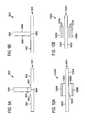
- FIG. 1shows a field-effect transistor 100 in accordance with a first exemplary embodiment of the invention.
- the field-effect transistor 100has an electrically semiconducting or metallically conductive first carbon nanotube 101 with a length of approximately up to 100 nm and a thickness of approximately 1 nm to 10 nm.
- the first carbon nanotube 101 and all the carbon nanotubes described below, including the carbon nanotubes of the further exemplary embodiments,are produced by means of a vapor deposition process, as described in [2], or by being grown on, as described in [3].
- the first carbon nanotube 101has a source region 102 , a channel region 103 and a drain region 104 of the field-effect transistor 100 .
- an insulator layer 105comprising silicon nitride or silicon dioxide is applied to the first carbon nanotube 101 by means of a CVD process or a sputtering process.
- the insulator layer 105has a thickness of approximately 2 nm to 5 nm and a length which is at least as great as the length of the channel region 103 .
- a second carbon nanotube 106is grown on the insulator layer, substantially perpendicular to the first carbon nanotube 101 , using the process described in [2], [3]
- the second carbon nanotube 106has a length of approximately 10 nm and a thickness of approximately 1 nm to 10 nm.
- the carbon nanotubes 101 , 106may also have a bent, i.e. curved shape, provided that the functionality described above is ensured.
- An electric driving voltage, the gate voltage,is applied to the second carbon nanotube 106 , which functions as the gate of the field-effect transistor, with the result that an electric field is generated.
- the electric fieldas a result of a field effect, changes the potential in the channel region 103 and thereby controls the electrical conductivity of the first carbon nanotube 101 .
- FIG. 2shows a field-effect transistor 200 in accordance with a second exemplary embodiment of the invention.
- the field-effect transistor 200differs from the field-effect transistor 100 in accordance with the first exemplary embodiment substantially through the fact that the first carbon nanotube 201 is formed by three carbon nanotubes 202 , 203 , 204 which are coupled to one another in an electrically conductive manner.
- a first part-nanotube 202which forms the source region of the field-effect transistor 200 , is a metallically conductive carbon nanotube.
- a second part-nanotube 203which forms the channel region of the field-effect transistor 200 , is a semiconducting carbon nanotube.
- a third part-nanotube 204which forms the drain region of the field-effect transistor 200 , is once again a metallically conductive carbon nanotube.
- the second part-nanotube 203is longer than the thickness of the second carbon nanotube 106 , i.e. in other words, the second part-nanotube 203 extends laterally beyond the diameter of the second carbon nanotube 106 .
- FIG. 3shows a field-effect transistor 300 in accordance with a third exemplary embodiment of the invention.
- the field-effect transistor 300differs from the field-effect transistor 200 in accordance with the second exemplary embodiment substantially through the fact that the second part-nanotube 203 is shorter than the thickness of the second carbon nanotube 106 , i.e. in other words, the second part-nanotube 203 , i.e. the extent of the channel region, is laterally shorter than the diameter of the second carbon nanotube 106 .
- the longer the channel region, for example the second part-nanotube 203the lower the leakage currents within the blocked field-effect transistor.
- the influence of the second carbon nanotube 106which forms the gate of the field-effect transistor, increases the shorter the channel region, for example the second part-nanotube 203 .
- FIG. 4shows a field-effect transistor 400 in accordance with a fourth exemplary embodiment of the invention.
- the first carbon nanotube 401 of the field-effect transistor 400has five part-nanotubes 402 , 403 , 404 , 405 , 406 .
- a first part-nanotube 402which forms the source region of the field-effect transistor 400 , is a metallically conductive carbon nanotube.
- the channel region of the field-effect transistor 400is formed by the second part-nanotube 403 , the third part-nanotube 404 and the fourth part-nanotube 405 , the second part-nanotube 403 being a semiconducting carbon nanotube, the third part-nanotube 404 being a metallically conductive carbon nanotube and the fourth part-nanotube 405 once again being a semiconducting carbon nanotube.
- the fifth part-nanotube 406which forms the drain region of the field-effect transistor 400 , is once again a metallically conductive carbon nanotube. Therefore, the channel region is generally formed by part-nanotubes, a semiconducting carbon nanotube being arranged at each end of the channel region, and any desired number of metallically conductive and semiconducting carbon nanotubes being arranged between them.
- the second carbon nanotube 407is gamma-shaped, i.e. the second carbon nanotube 407 has two branches 408 , 409 , or in general terms any desired number of branches, the branches 408 , 409 being arranged on the insulator layer 105 above the region of the second part-nanotube 403 and of the fourth part-nanotube 405 , with the result that the channel region of the field-effect transistor 400 can be widened in a simple way.
- FIG. 5shows a field-effect transistor 500 in accordance with a fifth exemplary embodiment of the invention.
- the field-effect transistor 500differs from the field-effect transistor 300 in accordance with the third exemplary embodiment substantially through the fact that a second insulator layer 501 is applied to the first carbon nanotube in the channel region of the transistor and a third carbon nanotube 502 is grown on the insulator layer.
- the third carbon nanotube 502is electrically coupled to the second carbon nanotube 106 , so that, as can be seen, a field-effect transistor 500 with a plurality of gates is formed.
- FIG. 6shows a field-effect transistor 600 in accordance with a sixth exemplary embodiment of the invention.
- the field-effect transistor 600differs from the field-effect transistor 300 in accordance with the third exemplary embodiment substantially through the fact that the second carbon nanotube is formed by a multiplicity, i.e. as it were, a bundle of carbon nanotubes 601 , which together are used as the gate of the field-effect transistor 600 .
- a common feature of the exemplary embodiment illustratedis that the flow of current of electrical charge carriers in the channel region of the controlled nanowire is controlled by means of the electric field generated at the gate region by means of the field effect which occurs as a result of an electric voltage being applied to the gate region of the respective field-effect transistor.
- FIG. 7Ashows a cross section through a field-effect transistor 700 in accordance with a seventh exemplary embodiment of the invention.
- the field-effect transistor 700has a semiconducting first carbon nanotube 701 , which forms a source-channel-drain structure of the field-effect transistor 700 , i.e. the semiconducting first carbon nanotube forms a source region 702 , a channel region 703 and a drain region 704 of the field-effect transistor 700 .
- the semiconducting first carbon nanotube 701is produced by means of the deposition process described in [2] or [3].
- a second carbon nanotube 705is applied to the semiconducting first carbon nanotube 701 .
- the second carbon nanotube 705is deposited on the first carbon nanotube 701 by means of the vapor deposition process described in [2] or [3].
- nanotubes which have already been produced and have three end regions, i.e. connections,can be used, as described, for example, in [8] as T-shaped or Y-shaped nanotubes.
- the second carbon nanotube 705which is electrically metallically conductive after it has been grown on or deposited, is converted into a boron nitride nanotube 707 in a predetermined region 708 which extends from a contact region 706 between the first carbon nanotube 701 and the second carbon nanotube 705 , along the second carbon nanotube 705 , with a predetermined length.
- a predetermined region 708which extends from a contact region 706 between the first carbon nanotube 701 and the second carbon nanotube 705 , along the second carbon nanotube 705 , with a predetermined length.
- the second carbon nanotube 705is doped with boron atoms and nitrogen atoms in a predetermined region using the process described in [6], so that the predetermined region 708 acquires an electrically insulating structure.
- the remaining region of the second carbon nanotube 705remains an electrically metallically conductive or semiconducting carbon nanotube, which according to this exemplary embodiment is denoted by reference numeral 709 .
- the electrically insulating region 708which has been doped with the boron atoms and the nitrogen atoms, of the field-effect transistor 700 , in the context of the field-effect transistor 700 which has been formed, acts as an insulator between the channel region 703 to which the second carbon nanotube 705 has been applied and the region 709 of the second carbon nanotube 705 which is still metallically conductive and functions as the gate region.
- the charge density of the electrical charge carriers in the channel region 703 and therefore the electrical conductivity of the channel region 703 of the field-effect transistor 700can be controlled by electrically driving the field-effect transistor 700 , in particular by applying an electric voltage to the gate region 709 of the second carbon nanotube 705 .
- the resulttherefore, is a field-effect transistor in which the electrical characteristics of a first carbon nanotube 701 can be controlled by means of a second carbon nanotube 705 as a result of an electric voltage being applied to the second carbon nanotube 705 .
- FIG. 7Bshows the associated profile of the walls of the first carbon nanotube 701 and of the second carbon nanotube 705 of the field-effect transistor 700 .
- the second carbon nanotube 705is applied to the first carbon nanotube 701 in such a manner that the walls 710 , 711 of the first carbon nanotube 701 are directly coupled to the wall 712 of the second carbon nanotube 705 in the contact region 706 .
- FIG. 8Ashows a field-effect transistor 800 in accordance with an eighth exemplary embodiment of the invention.
- the field-effect transistor 800has a first carbon nanotube 801 which, in the same way as the first carbon nanotube 701 of the field-effect transistor 700 in accordance with the seventh exemplary embodiment, forms the source-channel-drain structure of the field-effect transistor 800 .
- a first region of the first carbon nanotube 801is a region of an electrically metallically conductive carbon nanotube 802 which forms the source region of the field-effect transistor 800 .
- An electrically semiconducting nanotube region 803forms the channel region 803 of the field-effect transistor 800 .
- a metallically conductive carbon nanotube region 804 which adjoins the channel region 803forms the drain region of the field-effect transistor 800 .
- a second carbon nanotube 805is applied to the first carbon nanotube 801 on the channel region 803 of the first carbon nanotube 801 .
- the resultis a contact region 806 between the first carbon nanotube 801 and the second carbon nanotube 805 .
- the second carbon nanotube 805is doped with boron atoms or nitrogen atoms in a region 808 of predetermined size, so that an insulating region 807 is formed directly on the first carbon nanotube 801 .
- the remaining region of the second carbon nanotube 805remains electrically metallically conductive and forms the gate region 809 of the field-effect transistor 800 .
- FIG. 8Bshows the wall profile of the field-effect transistor 800 , once again showing that the walls 810 , 811 of the first carbon nanotube 801 clearly form a base to which the second carbon nanotube 805 is applied, and the walls 812 of the second carbon nanotube 805 being applied direct to the first carbon nanotube 801 , i.e. is coupled at contact locations 813 , 814 , which, according to this exemplary embodiment, given a cylindrical second carbon nanotube, has a circular structure.
- FIG. 9Ashows a field-effect transistor 900 in accordance with a ninth exemplary embodiment of the invention.
- a first carbon nanotube 905is applied as boron nitride nanotube to a silicon nanowire 901 , which forms the source-channel-drain structure of the field-effect transistor 900 and is electrically semiconducting, in the channel region 903 which is arranged between the source region 902 and the drain region 904 of the field-effect transistor 900 , so that a contact region 909 is formed between the silicon nanowire 901 and the first carbon nanotube 905 .
- a second carbon nanotube 906is applied, i.e. connected, to the first carbon nanotube 905 , the second carbon nanotube 906 forming the gate region of the field-effect transistor 900 and being designed as an electrically metallically conductive carbon nanotube.
- FIG. 9Bshows the wall profile of the field-effect transistor 900 .
- first carbon nanowire 905 and the second carbon nanowire 906which form a common unit, are applied to the silicon nanowire 901 , i.e. to its upper wall 907 , so that the side walls 908 of this unit are coupled in the contact region 906 .
- FIG. 10Ashows a field-effect transistor 1000 in accordance with a tenth exemplary embodiment of the invention.
- a first carbon nanotube 1001in accordance with this exemplary embodiment a carbon nanotube which is semiconducting all the way through, or alternatively a semiconducting silicon nanowire or a source-channel-drain structure of the field-effect transistor 1000 which is formed from a plurality of carbon nanotubes with different electrical properties, in accordance with the eighth exemplary embodiment, is provided.
- the first carbon nanotube 1001therefore once again forms a source region 1002 , a channel region 1003 and a drain region 1004 .
- a multi-walled second carbon nanotube 1005is applied to the channel region 1003 .
- the multi-walled boron nitride nanotube 1005serves as an insulator in the context of the field-effect transistor 1000 .
- a further, electrically metallically conductive carbon nanotube 1006which is used as gate of the field-effect transistor 1000 , is applied to the boron nitride nanotube 1005 .
- FIG. 10Bshows the wall profile which corresponds to the field-effect transistor 1000 and in which the walls 1007 of the first carbon nanotube 1001 , the walls 1008 of the multi-walled boron nitride nanotube 1005 and the walls 1009 of the second carbon nanotube 1006 are illustrated.
- the field-effect transistors presented abovecan also be formed as a result of the electrically insulating region 708 of the second carbon nanotube 705 , 805 , 906 being locally replaced by a boron nitride nanotube.
- controlled vapor-phase epitaxycan be produced using catalysts to grow the boron nitride nanotube or the metallically conductive carbon nanotube on the corresponding boron nitride nanotube using the process described in [3].
- the individual elements of the field-effect transistorcan be assembled using nanomanipulators.
- a carbon nanotube having the length of the desired region 708to be grown on the first nanowire, i.e. for example the first carbon nanotube, in the channel region of the field-effect transistor formed, using the process described in [3], for this carbon nanotube which has been formed to be doped with boron atoms and nitrogen atoms, so that a boron nitride nanotube is formed, and for the metallically conductive carbon nanotube to be grown on this boron nitride nanotube.
Landscapes
- Engineering & Computer Science (AREA)
- Chemical & Material Sciences (AREA)
- Nanotechnology (AREA)
- Materials Engineering (AREA)
- Physics & Mathematics (AREA)
- Mathematical Physics (AREA)
- Theoretical Computer Science (AREA)
- Crystallography & Structural Chemistry (AREA)
- Spectroscopy & Molecular Physics (AREA)
- Thin Film Transistor (AREA)
Abstract
Description
Claims (24)
Applications Claiming Priority (5)
| Application Number | Priority Date | Filing Date | Title |
|---|---|---|---|
| DE10032370ADE10032370C1 (en) | 2000-07-04 | 2000-07-04 | Carbon nanotube field effect transistor has two nanotubes spaced apart to prevent tunnel current between them |
| DE10032414.2 | 2000-07-04 | ||
| DE10032370.7 | 2000-07-04 | ||
| DE10032414ADE10032414C1 (en) | 2000-07-04 | 2000-07-04 | Field effect transistor used as a MOSFET comprises a nanowire, and nanotubes applied to the wire and having an electrically insulating region and a semiconducting region or a metallic region |
| PCT/DE2001/002451WO2002003482A1 (en) | 2000-07-04 | 2001-07-03 | Field effect transistor |
Publications (2)
| Publication Number | Publication Date |
|---|---|
| US20030148562A1 US20030148562A1 (en) | 2003-08-07 |
| US6798000B2true US6798000B2 (en) | 2004-09-28 |
Family
ID=26006267
Family Applications (1)
| Application Number | Title | Priority Date | Filing Date |
|---|---|---|---|
| US10/275,337Expired - Fee RelatedUS6798000B2 (en) | 2000-07-04 | 2001-07-03 | Field effect transistor |
Country Status (4)
| Country | Link |
|---|---|
| US (1) | US6798000B2 (en) |
| EP (1) | EP1299914B1 (en) |
| JP (1) | JP4112358B2 (en) |
| WO (1) | WO2002003482A1 (en) |
Cited By (96)
| Publication number | Priority date | Publication date | Assignee | Title |
|---|---|---|---|---|
| US20040112964A1 (en)* | 2002-09-30 | 2004-06-17 | Nanosys, Inc. | Applications of nano-enabled large area macroelectronic substrates incorporating nanowires and nanowire composites |
| US20040135951A1 (en)* | 2002-09-30 | 2004-07-15 | Dave Stumbo | Integrated displays using nanowire transistors |
| US20050051805A1 (en)* | 2003-08-19 | 2005-03-10 | Kim Byong Man | Nanotube transistor device |
| US20050079659A1 (en)* | 2002-09-30 | 2005-04-14 | Nanosys, Inc. | Large-area nanoenabled macroelectronic substrates and uses therefor |
| US20050167755A1 (en)* | 2003-01-02 | 2005-08-04 | Intel Corporation | Microcircuit fabrication and interconnection |
| US20050181587A1 (en)* | 2002-09-30 | 2005-08-18 | Nanosys, Inc. | Large-area nanoenabled macroelectronic substrates and uses therefor |
| US20050212079A1 (en)* | 2004-03-23 | 2005-09-29 | Nanosys, Inc. | Nanowire varactor diode and methods of making same |
| US20050224888A1 (en)* | 2002-10-31 | 2005-10-13 | Infineon Technologies Ag | Integrated circuit array |
| US20050237850A1 (en)* | 2003-10-02 | 2005-10-27 | Suman Datta | Method and apparatus for improving stability of a 6T CMOS SRAM cell |
| US20050242406A1 (en)* | 2003-06-27 | 2005-11-03 | Hareland Scott A | Nonplanar device with stress incorporation layer and method of fabrication |
| US20050279274A1 (en)* | 2004-04-30 | 2005-12-22 | Chunming Niu | Systems and methods for nanowire growth and manufacturing |
| US20060009003A1 (en)* | 2004-07-07 | 2006-01-12 | Nanosys, Inc. | Methods for nanowire growth |
| US20060011972A1 (en)* | 2002-10-31 | 2006-01-19 | Andrew Graham | Non-volatile memory cell, memory cell arrangement and method for production of a non-volatile memory cell |
| US20060019472A1 (en)* | 2004-04-30 | 2006-01-26 | Nanosys, Inc. | Systems and methods for nanowire growth and harvesting |
| US20060033095A1 (en)* | 2004-08-10 | 2006-02-16 | Doyle Brian S | Non-planar pMOS structure with a strained channel region and an integrated strained CMOS flow |
| US20060081886A1 (en)* | 2004-10-15 | 2006-04-20 | Nanosys, Inc. | Method, system and apparatus for gating configurations and improved contacts in nanowire-based electronic devices |
| US7049625B2 (en) | 2002-03-18 | 2006-05-23 | Max-Planck-Gesellschaft Zur Fonderung Der Wissenschaften E.V. | Field effect transistor memory cell, memory device and method for manufacturing a field effect transistor memory cell |
| US20060214156A1 (en)* | 2004-10-12 | 2006-09-28 | Nanosys, Inc. | Fully integrated organic layered processes for making plastic electronics based on conductive polymers and semiconductor nanowires |
| US20060244361A1 (en)* | 2005-03-28 | 2006-11-02 | Kim Ki-Nam | Vertical type nanotube semiconductor device and method of manufacturing the same |
| US20060273328A1 (en)* | 2005-06-02 | 2006-12-07 | Nanosys, Inc. | Light emitting nanowires for macroelectronics |
| US20060286023A1 (en)* | 2004-08-02 | 2006-12-21 | Houjin Huang | Carbon nanotube, method for positioning the same, field-effect transistor made using the carbon nanotube, method for making the field-effect transistor, and semiconductor device |
| US20070001220A1 (en)* | 2004-09-16 | 2007-01-04 | Atomate Corporation | Nanotube Transistor and Rectifying Devices |
| US20070023839A1 (en)* | 2005-07-27 | 2007-02-01 | International Business Machines Corporation | Finfet gate formed of carbon nanotubes |
| US20070134878A1 (en)* | 2005-12-09 | 2007-06-14 | Intel Corporation | Non-planar microelectronic device having isolation element to mitigate fringe effects and method to fabricate same |
| US20070131983A1 (en)* | 2005-12-13 | 2007-06-14 | Intel Corporation | Tri-gate integration with embedded floating body memory cell using a high-K dual metal gate |
| US20070138514A1 (en)* | 2005-12-21 | 2007-06-21 | Chang Peter L | Integration of planar and tri-gate devices on the same substrate |
| US20070148926A1 (en)* | 2005-12-28 | 2007-06-28 | Intel Corporation | Dual halo implant for improving short channel effect in three-dimensional tri-gate transistors |
| EP1804286A1 (en) | 2005-12-27 | 2007-07-04 | Interuniversitair Microelektronica Centrum | Elongate nanostructure semiconductor device |
| US20070176824A1 (en)* | 2002-09-30 | 2007-08-02 | Nanosys Inc. | Phased array systems and methods |
| US20070190880A1 (en)* | 2004-02-02 | 2007-08-16 | Nanosys, Inc. | Porous substrates, articles, systems and compositions comprising nanofibers and methods of their use and production |
| US20070231997A1 (en)* | 2006-03-31 | 2007-10-04 | Doyle Brian S | Stacked multi-gate transistor design and method of fabrication |
| US20070231984A1 (en)* | 2006-03-31 | 2007-10-04 | Metz Matthew V | Uniform silicide metal on epitaxially grown source and drain regions of three-dimensional transistors |
| US20070238273A1 (en)* | 2006-03-31 | 2007-10-11 | Doyle Brian S | Method of ion implanting for tri-gate devices |
| US20070235763A1 (en)* | 2006-03-29 | 2007-10-11 | Doyle Brian S | Substrate band gap engineered multi-gate pMOS devices |
| US20070262397A1 (en)* | 2004-07-16 | 2007-11-15 | Koninklijke Philips Electronics N.V. | Nanoscale Fet |
| US20080038520A1 (en)* | 2005-12-29 | 2008-02-14 | Nanosys, Inc. | Methods for oriented growth of nanowires on patterned substrates |
| US20080068876A1 (en)* | 2006-09-20 | 2008-03-20 | Micron Technology, Inc. | Reduced leakage memory cells |
| US7361958B2 (en) | 2004-09-30 | 2008-04-22 | Intel Corporation | Nonplanar transistors with metal gate electrodes |
| US20080097346A1 (en)* | 2006-09-19 | 2008-04-24 | Alcon, Inc. | Trocar cannula |
| US20080121998A1 (en)* | 2006-09-15 | 2008-05-29 | Kavalieros Jack T | Apparatus and method for selectively recessing spacers on multi-gate devices |
| US20080150165A1 (en)* | 2006-11-29 | 2008-06-26 | Nanosys, Inc. | Selective processing of semiconductor nanowires by polarized visible radiation |
| US20080157061A1 (en)* | 2007-01-03 | 2008-07-03 | U.S.A. As Represented By The Secretary Of The Army | Field effect transistor array using single wall carbon nano-tubes |
| US7396711B2 (en) | 2005-12-27 | 2008-07-08 | Intel Corporation | Method of fabricating a multi-cornered film |
| US20080179586A1 (en)* | 2007-01-29 | 2008-07-31 | Kamins Theodore I | Electronic device and method of making the same |
| US20080200028A1 (en)* | 2002-04-02 | 2008-08-21 | Nanosys, Inc. | Methods of positioning and/or orienting nanostructures |
| US20080272361A1 (en)* | 2007-05-02 | 2008-11-06 | Atomate Corporation | High Density Nanotube Devices |
| US7456476B2 (en) | 2003-06-27 | 2008-11-25 | Intel Corporation | Nonplanar semiconductor device with partially or fully wrapped around gate electrode and methods of fabrication |
| US7462890B1 (en) | 2004-09-16 | 2008-12-09 | Atomate Corporation | Nanotube transistor integrated circuit layout |
| US7479421B2 (en) | 2005-09-28 | 2009-01-20 | Intel Corporation | Process for integrating planar and non-planar CMOS transistors on a bulk substrate and article made thereby |
| US7518196B2 (en) | 2005-02-23 | 2009-04-14 | Intel Corporation | Field effect transistor with narrow bandgap source and drain regions and method of fabrication |
| US7525160B2 (en) | 2005-12-27 | 2009-04-28 | Intel Corporation | Multigate device with recessed strain regions |
| US20090127540A1 (en)* | 2006-11-07 | 2009-05-21 | Nanosys, Inc. | Systems and Methods for Nanowire Growth |
| US20090143227A1 (en)* | 2004-02-02 | 2009-06-04 | Nanosys, Inc. | Porous substrates, articles, systems and compositions comprising nanofibers and methods of their use and production |
| US7547637B2 (en) | 2005-06-21 | 2009-06-16 | Intel Corporation | Methods for patterning a semiconductor film |
| US7550333B2 (en) | 2004-10-25 | 2009-06-23 | Intel Corporation | Nonplanar device with thinned lower body portion and method of fabrication |
| US20090166686A1 (en)* | 2007-12-31 | 2009-07-02 | Atomate Corporation | Edge-Contacted Vertical Carbon Nanotube Transistor |
| US7560366B1 (en) | 2004-12-02 | 2009-07-14 | Nanosys, Inc. | Nanowire horizontal growth and substrate removal |
| US7569503B2 (en) | 2004-11-24 | 2009-08-04 | Nanosys, Inc. | Contact doping and annealing systems and processes for nanowire thin films |
| US7579280B2 (en) | 2004-06-01 | 2009-08-25 | Intel Corporation | Method of patterning a film |
| US20090213830A1 (en)* | 2004-10-11 | 2009-08-27 | Qimonda Ag | Communication system |
| US20090258438A1 (en)* | 2008-04-09 | 2009-10-15 | Maki Wusi C | Method for universal biodetection of antigens and biomolecules |
| US20090285030A1 (en)* | 2005-01-26 | 2009-11-19 | Kang Dong-Hun | Multi-bit nonvolatile memory devices and methods of operating the same |
| US20100065820A1 (en)* | 2005-02-14 | 2010-03-18 | Atomate Corporation | Nanotube Device Having Nanotubes with Multiple Characteristics |
| US7700470B2 (en) | 2006-09-22 | 2010-04-20 | Intel Corporation | Selective anisotropic wet etching of workfunction metal for semiconductor devices |
| US7736956B2 (en) | 2005-08-17 | 2010-06-15 | Intel Corporation | Lateral undercut of metal gate in SOI device |
| US7741197B1 (en) | 2005-12-29 | 2010-06-22 | Nanosys, Inc. | Systems and methods for harvesting and reducing contamination in nanowires |
| US20100155801A1 (en)* | 2008-12-22 | 2010-06-24 | Doyle Brian S | Integrated circuit, 1T-1C embedded memory cell containing same, and method of manufacturing 1T-1C memory cell for embedded memory application |
| US20100163945A1 (en)* | 2008-12-30 | 2010-07-01 | Kavalieros Jack T | Embedded memory cell and method of manufacturing same |
| US20100167512A1 (en)* | 2005-09-23 | 2010-07-01 | Nanosys, Inc. | Methods for Nanostructure Doping |
| US20100173478A1 (en)* | 2004-09-16 | 2010-07-08 | Atomate Corporation | Concentric gate nanotube transistor devices |
| US7781771B2 (en) | 2004-03-31 | 2010-08-24 | Intel Corporation | Bulk non-planar transistor having strained enhanced mobility and methods of fabrication |
| US7785922B2 (en) | 2004-04-30 | 2010-08-31 | Nanosys, Inc. | Methods for oriented growth of nanowires on patterned substrates |
| US20100252800A1 (en)* | 2009-04-03 | 2010-10-07 | International Business Machines Corporation | Nanowire devices for enhancing mobility through stress engineering |
| US20100252814A1 (en)* | 2009-04-03 | 2010-10-07 | International Business Machines Corporation | Semiconductor nanowires having mobility-optimized orientations |
| US20100252815A1 (en)* | 2009-04-03 | 2010-10-07 | International Business Machines Corporation | Structurally stabilized semiconductor nanowire |
| US20100252801A1 (en)* | 2009-04-03 | 2010-10-07 | International Business Machines Corporation | Semiconductor nanowire with built-in stress |
| US7859053B2 (en) | 2004-09-29 | 2010-12-28 | Intel Corporation | Independently accessed double-gate and tri-gate transistors in same process flow |
| US20110012177A1 (en)* | 2009-07-20 | 2011-01-20 | International Business Machines Corporation | Nanostructure For Changing Electric Mobility |
| US20110012176A1 (en)* | 2009-07-20 | 2011-01-20 | International Business Machines Corporation | Multiple Orientation Nanowires With Gate Stack Stressors |
| US7879675B2 (en) | 2005-03-14 | 2011-02-01 | Intel Corporation | Field effect transistor with metal source/drain regions |
| US20110045660A1 (en)* | 2002-09-30 | 2011-02-24 | Nanosys, Inc. | Large-Area Nanoenabled Macroelectronic Substrates and Uses Therefor |
| US7898041B2 (en) | 2005-06-30 | 2011-03-01 | Intel Corporation | Block contact architectures for nanoscale channel transistors |
| US7902014B2 (en) | 2005-09-28 | 2011-03-08 | Intel Corporation | CMOS devices with a single work function gate electrode and method of fabrication |
| US7911234B1 (en) | 2007-09-28 | 2011-03-22 | The Board Of Trustees Of The Leland Stanford Junior University | Nanotube logic circuits |
| US7915167B2 (en) | 2004-09-29 | 2011-03-29 | Intel Corporation | Fabrication of channel wraparound gate structure for field-effect transistor |
| US20110081770A1 (en)* | 2004-09-16 | 2011-04-07 | Atomate Corporation | Removing undesirable nanotubes during nanotube device fabrication |
| US7989280B2 (en) | 2005-11-30 | 2011-08-02 | Intel Corporation | Dielectric interface for group III-V semiconductor device |
| US8084818B2 (en) | 2004-06-30 | 2011-12-27 | Intel Corporation | High mobility tri-gate devices and methods of fabrication |
| US8168495B1 (en) | 2006-12-29 | 2012-05-01 | Etamota Corporation | Carbon nanotube high frequency transistor technology |
| US8362566B2 (en) | 2008-06-23 | 2013-01-29 | Intel Corporation | Stress in trigate devices using complimentary gate fill materials |
| US8390066B2 (en) | 2010-03-15 | 2013-03-05 | Kabushiki Kaisha Toshiba | Semiconductor nanowire memory device |
| US8617945B2 (en) | 2006-08-02 | 2013-12-31 | Intel Corporation | Stacking fault and twin blocking barrier for integrating III-V on Si |
| US9337307B2 (en) | 2005-06-15 | 2016-05-10 | Intel Corporation | Method for fabricating transistor with thinned channel |
| US9825154B2 (en)* | 2011-11-28 | 2017-11-21 | Michigan Technological University | Room temperature tunneling switches and methods of making and using the same |
| US10279341B2 (en) | 2004-02-02 | 2019-05-07 | Oned Material Llc | Porous substrates, articles, systems and compositions comprising nanofibers and methods of their use and production |
| US10490817B2 (en) | 2009-05-19 | 2019-11-26 | Oned Material Llc | Nanostructured materials for battery applications |
Families Citing this family (37)
| Publication number | Priority date | Publication date | Assignee | Title |
|---|---|---|---|---|
| US7084507B2 (en) | 2001-05-02 | 2006-08-01 | Fujitsu Limited | Integrated circuit device and method of producing the same |
| US7385262B2 (en)* | 2001-11-27 | 2008-06-10 | The Board Of Trustees Of The Leland Stanford Junior University | Band-structure modulation of nano-structures in an electric field |
| EP1341184B1 (en)* | 2002-02-09 | 2005-09-14 | Samsung Electronics Co., Ltd. | Memory device utilizing carbon nanotubes and method of fabricating the memory device |
| US6891227B2 (en)* | 2002-03-20 | 2005-05-10 | International Business Machines Corporation | Self-aligned nanotube field effect transistor and method of fabricating same |
| JP3969228B2 (en)* | 2002-07-19 | 2007-09-05 | 松下電工株式会社 | Mechanical deformation detection sensor, acceleration sensor using the same, and pressure sensor |
| ATE421147T1 (en)* | 2002-07-25 | 2009-01-15 | California Inst Of Techn | THREE-DIMENSIONAL STORAGE ARRAY |
| JP2006501690A (en)* | 2002-09-30 | 2006-01-12 | ナノシス・インコーポレイテッド | Applications of large-area macroelectronic substrates incorporating nano-enabled, nanowires and nanowire hybrids |
| KR100790859B1 (en)* | 2002-11-15 | 2008-01-03 | 삼성전자주식회사 | Nonvolatile Memory Devices Using Vertical Nanotubes |
| US6936496B2 (en)* | 2002-12-20 | 2005-08-30 | Hewlett-Packard Development Company, L.P. | Nanowire filament |
| EP1645871B1 (en)* | 2003-05-23 | 2016-04-06 | Japan Science and Technology Agency | Carbon nanotube field-effect transistor |
| DE10324081B4 (en)* | 2003-05-27 | 2005-11-17 | Infineon Technologies Ag | Storage device for storing electrical charge and method for producing the same |
| US7132298B2 (en)* | 2003-10-07 | 2006-11-07 | Hewlett-Packard Development Company, L.P. | Fabrication of nano-object array |
| US7223611B2 (en)* | 2003-10-07 | 2007-05-29 | Hewlett-Packard Development Company, L.P. | Fabrication of nanowires |
| US7692249B2 (en)* | 2004-01-21 | 2010-04-06 | Intel Corporation | End functionalization of carbon nanotubes |
| US7407738B2 (en)* | 2004-04-02 | 2008-08-05 | Pavel Kornilovich | Fabrication and use of superlattice |
| US7683435B2 (en)* | 2004-04-30 | 2010-03-23 | Hewlett-Packard Development Company, L.P. | Misalignment-tolerant multiplexing/demultiplexing architectures |
| US7247531B2 (en)* | 2004-04-30 | 2007-07-24 | Hewlett-Packard Development Company, L.P. | Field-effect-transistor multiplexing/demultiplexing architectures and methods of forming the same |
| US20050241959A1 (en)* | 2004-04-30 | 2005-11-03 | Kenneth Ward | Chemical-sensing devices |
| US7727820B2 (en)* | 2004-04-30 | 2010-06-01 | Hewlett-Packard Development Company, L.P. | Misalignment-tolerant methods for fabricating multiplexing/demultiplexing architectures |
| US20060086994A1 (en)* | 2004-05-14 | 2006-04-27 | Susanne Viefers | Nanoelectromechanical components |
| US7180107B2 (en)* | 2004-05-25 | 2007-02-20 | International Business Machines Corporation | Method of fabricating a tunneling nanotube field effect transistor |
| JP4488815B2 (en)* | 2004-07-13 | 2010-06-23 | シャープ株式会社 | Device, integrated circuit and manufacturing method thereof |
| US20060024814A1 (en)* | 2004-07-29 | 2006-02-02 | Peters Kevin F | Aptamer-functionalized electrochemical sensors and methods of fabricating and using the same |
| KR101025846B1 (en)* | 2004-09-13 | 2011-03-30 | 삼성전자주식회사 | Transistors in Semiconductor Devices Containing Carbon Nanotube Channels |
| US7365395B2 (en)* | 2004-09-16 | 2008-04-29 | Nanosys, Inc. | Artificial dielectrics using nanostructures |
| US7598516B2 (en)* | 2005-01-07 | 2009-10-06 | International Business Machines Corporation | Self-aligned process for nanotube/nanowire FETs |
| US7598544B2 (en)* | 2005-01-14 | 2009-10-06 | Nanotero, Inc. | Hybrid carbon nanotude FET(CNFET)-FET static RAM (SRAM) and method of making same |
| US8362525B2 (en)* | 2005-01-14 | 2013-01-29 | Nantero Inc. | Field effect device having a channel of nanofabric and methods of making same |
| JP4904696B2 (en)* | 2005-02-16 | 2012-03-28 | 日本電気株式会社 | Field effect transistor and manufacturing method thereof |
| US7375012B2 (en)* | 2005-02-28 | 2008-05-20 | Pavel Kornilovich | Method of forming multilayer film |
| US7479654B2 (en) | 2005-05-09 | 2009-01-20 | Nantero, Inc. | Memory arrays using nanotube articles with reprogrammable resistance |
| US7611906B2 (en)* | 2006-01-23 | 2009-11-03 | Applied Nanotech Holdings, Inc. | Functionalized carbon nanotubes |
| JP5171161B2 (en)* | 2006-09-15 | 2013-03-27 | アイメック | Nanowire tunnel field effect transistor semiconductor device and manufacturing method thereof |
| WO2009029921A1 (en)* | 2007-08-31 | 2009-03-05 | Magsil Corporation | High density magnetic memory based on nanotubes |
| US8748950B2 (en) | 2009-11-19 | 2014-06-10 | University of Pittsburgh—of the Commonwealth System of Higher Education | On-demand nanoelectronics platform |
| US20110233513A1 (en)* | 2010-03-29 | 2011-09-29 | International Business Machines Corporation | Enhanced bonding interfaces on carbon-based materials for nanoelectronic devices |
| US9287516B2 (en)* | 2014-04-07 | 2016-03-15 | International Business Machines Corporation | Forming pn junction contacts by different dielectrics |
Citations (2)
| Publication number | Priority date | Publication date | Assignee | Title |
|---|---|---|---|---|
| WO1999004440A1 (en) | 1997-07-14 | 1999-01-28 | Technion Research And Development Foundation Ltd. | Microelectronic components and electronic networks comprising dna |
| WO2000051186A1 (en)* | 1999-02-22 | 2000-08-31 | Clawson Joseph E Jr | Nanostructure device and apparatus |
- 2001
- 2001-07-03EPEP01953838Apatent/EP1299914B1/ennot_activeExpired - Lifetime
- 2001-07-03JPJP2002507461Apatent/JP4112358B2/ennot_activeExpired - Fee Related
- 2001-07-03USUS10/275,337patent/US6798000B2/ennot_activeExpired - Fee Related
- 2001-07-03WOPCT/DE2001/002451patent/WO2002003482A1/enactiveIP Right Grant
Patent Citations (2)
| Publication number | Priority date | Publication date | Assignee | Title |
|---|---|---|---|---|
| WO1999004440A1 (en) | 1997-07-14 | 1999-01-28 | Technion Research And Development Foundation Ltd. | Microelectronic components and electronic networks comprising dna |
| WO2000051186A1 (en)* | 1999-02-22 | 2000-08-31 | Clawson Joseph E Jr | Nanostructure device and apparatus |
Non-Patent Citations (10)
| Title |
|---|
| Chung, Sung-Wook et al., Silicon nanowire devices, Applied Physics Letters, vol. 78, No. 15, pp. 2068-2070 (1999). |
| Dekker, C., Carbon Nanotubes as Molecular Quantum Wires, Physics Today, pp. 22-28, May, 1999. |
| Han, W. et al., Synthesis of Boron Nitride Nanotubes from Carbon Nanotubes by a Substitution Reaction, Applied Physics Letters, vol. 73, No. 21, pp. 3085-3087, Nov. 1998. |
| Hu, J., et al., Controlled growth and electrical properties of heterojunctions of carbon nanotubes and silicon nanowires, Nature, vol. 399, pp. 48-51, May, 1999. |
| Martel, R. et al., Single- and multi-wall carbon nanotube field-effect transistors, Applied Physics Letters, vol. 73, No. 17, pp. 2447-2449, Oct. 1998. |
| Menon, M. and Srivastava, D., Carbon Nanotube "T Junctions": Nanoscale Metal-Semiconductor Metal Contact Devices, Physics Review Letters, vol. 79, No. 22, pp. 4453-4456, Dec. 1997. |
| Ren Z.F. et al., Synthesis of Large Arrays of Well-Aligned Carbon Nanotubes on Glass, Science, vol. 282, pp. 1105-1107, Nov. 1998. |
| Shea H.R. et al., Manipulation of Carbon Nanotubes and Properties of Nanolube Field-Effect Transistors and Rings, Microelectronic Engineering, Elsevier Publishers BV, vol. 46, No. 1-4, pp.101-104 (1999). |
| Suh, Jung Sang and Lee, Jin Seung, Highly ordered two-dimensional carbon nanotube arrays, Applied Physics Letters, vol. 75, No. 14, pp. 2047-2049, Oct. 1999. |
| Vedeneev A.S. et al., Molecular Scale Rectifying Diodes Based on Y Junction Carbon Nanotubes, Proceedings of the IEDM Conference, IEDM 99, pp. 231-233 (1999). |
Cited By (250)
| Publication number | Priority date | Publication date | Assignee | Title |
|---|---|---|---|---|
| US7049625B2 (en) | 2002-03-18 | 2006-05-23 | Max-Planck-Gesellschaft Zur Fonderung Der Wissenschaften E.V. | Field effect transistor memory cell, memory device and method for manufacturing a field effect transistor memory cell |
| US7422980B1 (en) | 2002-04-02 | 2008-09-09 | Nanosys, Inc. | Methods of positioning and/or orienting nanostructures |
| US20080200028A1 (en)* | 2002-04-02 | 2008-08-21 | Nanosys, Inc. | Methods of positioning and/or orienting nanostructures |
| US20080293244A1 (en)* | 2002-04-02 | 2008-11-27 | Nanosys, Inc. | Methods of Positioning and/or Orienting Nanostructures |
| US7651944B2 (en) | 2002-04-02 | 2010-01-26 | Nanosys, Inc. | Methods of positioning and/or orienting nanostructures |
| US20100155696A1 (en)* | 2002-09-30 | 2010-06-24 | Nanosys, Inc. | Large-Area Nanoenabled Macroelectronic Substrates and Uses Therefor |
| US7135728B2 (en) | 2002-09-30 | 2006-11-14 | Nanosys, Inc. | Large-area nanoenabled macroelectronic substrates and uses therefor |
| US20050199731A9 (en)* | 2002-09-30 | 2005-09-15 | Nanosys, Inc. | Applications of nano-enabled large area macroelectronic substrates incorporating nanowires and nanowire composites |
| US7427328B2 (en) | 2002-09-30 | 2008-09-23 | Nanosys, Inc. | Large-area nanoenabled macroelectronic substrates and uses therefor |
| US7619562B2 (en) | 2002-09-30 | 2009-11-17 | Nanosys, Inc. | Phased array systems |
| US20040135951A1 (en)* | 2002-09-30 | 2004-07-15 | Dave Stumbo | Integrated displays using nanowire transistors |
| US20110045660A1 (en)* | 2002-09-30 | 2011-02-24 | Nanosys, Inc. | Large-Area Nanoenabled Macroelectronic Substrates and Uses Therefor |
| US20050079659A1 (en)* | 2002-09-30 | 2005-04-14 | Nanosys, Inc. | Large-area nanoenabled macroelectronic substrates and uses therefor |
| US7932511B2 (en) | 2002-09-30 | 2011-04-26 | Nanosys, Inc. | Large-area nanoenabled macroelectronic substrates and uses therefor |
| US20070120167A1 (en)* | 2002-09-30 | 2007-05-31 | Nanosys, Inc. | Large-area nanoenabled macroelectronic substrates and uses therefor |
| US20040112964A1 (en)* | 2002-09-30 | 2004-06-17 | Nanosys, Inc. | Applications of nano-enabled large area macroelectronic substrates incorporating nanowires and nanowire composites |
| US20070012980A1 (en)* | 2002-09-30 | 2007-01-18 | Nanosys, Inc. | Large-area nanoenabled macroelectronic substrates and uses therefor |
| US8030186B2 (en) | 2002-09-30 | 2011-10-04 | Nanosys, Inc. | Large-area nanoenabled macroelectronic substrates and uses therefor |
| US7701428B2 (en) | 2002-09-30 | 2010-04-20 | Nanosys, Inc. | Integrated displays using nanowire transistors |
| US20050110064A1 (en)* | 2002-09-30 | 2005-05-26 | Nanosys, Inc. | Large-area nanoenabled macroelectronic substrates and uses therefor |
| US7051945B2 (en) | 2002-09-30 | 2006-05-30 | Nanosys, Inc | Applications of nano-enabled large area macroelectronic substrates incorporating nanowires and nanowire composites |
| US7064372B2 (en) | 2002-09-30 | 2006-06-20 | Nanosys, Inc. | Large-area nanoenabled macroelectronic substrates and uses therefor |
| US7067867B2 (en)* | 2002-09-30 | 2006-06-27 | Nanosys, Inc. | Large-area nonenabled macroelectronic substrates and uses therefor |
| US20060151820A1 (en)* | 2002-09-30 | 2006-07-13 | Nanosys, Inc. | Large-area nanoenabled macroelectronic substrates and uses therefor |
| US7083104B1 (en) | 2002-09-30 | 2006-08-01 | Nanosys, Inc. | Applications of nano-enabled large area macroelectronic substrates incorporating nanowires and nanowire composites |
| US20060169788A1 (en)* | 2002-09-30 | 2006-08-03 | Nanosys, Inc. | Applications of nano-enabled large area macroelectronic substrates incorporating nanowires and nanowire composites |
| US7102605B2 (en) | 2002-09-30 | 2006-09-05 | Nanosys, Inc. | Integrated displays using nanowire transistors |
| US7233041B2 (en) | 2002-09-30 | 2007-06-19 | Nanosys, Inc. | Large-area nanoenabled macroelectronic substrates and uses therefor |
| US20060211183A1 (en)* | 2002-09-30 | 2006-09-21 | Nanosys, Inc. | Large-area nanoenabled macroelectronic substrates and uses therefor |
| US20050181587A1 (en)* | 2002-09-30 | 2005-08-18 | Nanosys, Inc. | Large-area nanoenabled macroelectronic substrates and uses therefor |
| US8293624B2 (en) | 2002-09-30 | 2012-10-23 | Nanosys, Inc. | Large area nanoenabled macroelectronic substrates and uses therefor |
| US20060237537A1 (en)* | 2002-09-30 | 2006-10-26 | Nanosys, Inc. | Applications of nano-enabled large area macroelectronic substrates incorporating nanowires and nanowire composites |
| US20070228439A1 (en)* | 2002-09-30 | 2007-10-04 | Nanosys, Inc. | Large-Area Nanoenabled Macroelectronic Substrates and Uses Therefor |
| US7851841B2 (en) | 2002-09-30 | 2010-12-14 | Nanosys, Inc. | Large-area nanoenabled macroelectronic substrates and uses therefor |
| US20060256059A1 (en)* | 2002-09-30 | 2006-11-16 | Nanosys, Inc. | Integrated displays using nanowire transistors |
| US20070176824A1 (en)* | 2002-09-30 | 2007-08-02 | Nanosys Inc. | Phased array systems and methods |
| US7262501B2 (en) | 2002-09-30 | 2007-08-28 | Nanosys, Inc. | Large-area nanoenabled macroelectronic substrates and uses therefor |
| US7265376B2 (en)* | 2002-10-31 | 2007-09-04 | Infineon Technologies, Inc. | Non-volatile memory cell, memory cell arrangement and method for production of a non-volatile memory cell |
| US20060011972A1 (en)* | 2002-10-31 | 2006-01-19 | Andrew Graham | Non-volatile memory cell, memory cell arrangement and method for production of a non-volatile memory cell |
| US20050224888A1 (en)* | 2002-10-31 | 2005-10-13 | Infineon Technologies Ag | Integrated circuit array |
| US7348675B2 (en) | 2003-01-02 | 2008-03-25 | Intel Corporation | Microcircuit fabrication and interconnection |
| US20050167755A1 (en)* | 2003-01-02 | 2005-08-04 | Intel Corporation | Microcircuit fabrication and interconnection |
| US20080119016A1 (en)* | 2003-01-02 | 2008-05-22 | Dubin Valery M | Microcircuit fabrication and interconnection |
| US7470620B2 (en) | 2003-01-02 | 2008-12-30 | Intel Corporation | Microcircuit fabrication and interconnection |
| US8405164B2 (en) | 2003-06-27 | 2013-03-26 | Intel Corporation | Tri-gate transistor device with stress incorporation layer and method of fabrication |
| US8273626B2 (en) | 2003-06-27 | 2012-09-25 | Intel Corporationn | Nonplanar semiconductor device with partially or fully wrapped around gate electrode and methods of fabrication |
| US20050242406A1 (en)* | 2003-06-27 | 2005-11-03 | Hareland Scott A | Nonplanar device with stress incorporation layer and method of fabrication |
| US7456476B2 (en) | 2003-06-27 | 2008-11-25 | Intel Corporation | Nonplanar semiconductor device with partially or fully wrapped around gate electrode and methods of fabrication |
| US7241653B2 (en) | 2003-06-27 | 2007-07-10 | Intel Corporation | Nonplanar device with stress incorporation layer and method of fabrication |
| US7820513B2 (en) | 2003-06-27 | 2010-10-26 | Intel Corporation | Nonplanar semiconductor device with partially or fully wrapped around gate electrode and methods of fabrication |
| US7714397B2 (en) | 2003-06-27 | 2010-05-11 | Intel Corporation | Tri-gate transistor device with stress incorporation layer and method of fabrication |
| US20050051805A1 (en)* | 2003-08-19 | 2005-03-10 | Kim Byong Man | Nanotube transistor device |
| US7445980B2 (en) | 2003-10-02 | 2008-11-04 | Intel Corporation | Method and apparatus for improving stability of a 6T CMOS SRAM cell |
| US20050237850A1 (en)* | 2003-10-02 | 2005-10-27 | Suman Datta | Method and apparatus for improving stability of a 6T CMOS SRAM cell |
| US20060281236A1 (en)* | 2003-10-02 | 2006-12-14 | Suman Datta | Method and apparatus for improving stability of a 6T CMOS SRAM cell |
| US7553371B2 (en) | 2004-02-02 | 2009-06-30 | Nanosys, Inc. | Porous substrates, articles, systems and compositions comprising nanofibers and methods of their use and production |
| US10279341B2 (en) | 2004-02-02 | 2019-05-07 | Oned Material Llc | Porous substrates, articles, systems and compositions comprising nanofibers and methods of their use and production |
| US20070190880A1 (en)* | 2004-02-02 | 2007-08-16 | Nanosys, Inc. | Porous substrates, articles, systems and compositions comprising nanofibers and methods of their use and production |
| US20090143227A1 (en)* | 2004-02-02 | 2009-06-04 | Nanosys, Inc. | Porous substrates, articles, systems and compositions comprising nanofibers and methods of their use and production |
| US8025960B2 (en) | 2004-02-02 | 2011-09-27 | Nanosys, Inc. | Porous substrates, articles, systems and compositions comprising nanofibers and methods of their use and production |
| US7115971B2 (en) | 2004-03-23 | 2006-10-03 | Nanosys, Inc. | Nanowire varactor diode and methods of making same |
| US20050212079A1 (en)* | 2004-03-23 | 2005-09-29 | Nanosys, Inc. | Nanowire varactor diode and methods of making same |
| US7667296B2 (en) | 2004-03-23 | 2010-02-23 | Nanosys, Inc. | Nanowire capacitor and methods of making same |
| US7781771B2 (en) | 2004-03-31 | 2010-08-24 | Intel Corporation | Bulk non-planar transistor having strained enhanced mobility and methods of fabrication |
| US7785922B2 (en) | 2004-04-30 | 2010-08-31 | Nanosys, Inc. | Methods for oriented growth of nanowires on patterned substrates |
| US20060255481A1 (en)* | 2004-04-30 | 2006-11-16 | Nanosys, Inc. | Systems and methods for nanowire growth and harvesting |
| US7105428B2 (en) | 2004-04-30 | 2006-09-12 | Nanosys, Inc. | Systems and methods for nanowire growth and harvesting |
| US7273732B2 (en) | 2004-04-30 | 2007-09-25 | Nanosys, Inc. | Systems and methods for nanowire growth and harvesting |
| US20100279513A1 (en)* | 2004-04-30 | 2010-11-04 | Nanosys, Inc. | Systems and Methods for Nanowire Growth and Manufacturing |
| US7666791B2 (en) | 2004-04-30 | 2010-02-23 | Nanosys, Inc. | Systems and methods for nanowire growth and harvesting |
| US20050279274A1 (en)* | 2004-04-30 | 2005-12-22 | Chunming Niu | Systems and methods for nanowire growth and manufacturing |
| US20080072818A1 (en)* | 2004-04-30 | 2008-03-27 | Nanosys, Inc. | Systems and Methods for Nanowire Growth and Harvesting |
| US7985454B2 (en) | 2004-04-30 | 2011-07-26 | Nanosys, Inc. | Systems and methods for nanowire growth and manufacturing |
| US20060019472A1 (en)* | 2004-04-30 | 2006-01-26 | Nanosys, Inc. | Systems and methods for nanowire growth and harvesting |
| US7579280B2 (en) | 2004-06-01 | 2009-08-25 | Intel Corporation | Method of patterning a film |
| US8084818B2 (en) | 2004-06-30 | 2011-12-27 | Intel Corporation | High mobility tri-gate devices and methods of fabrication |
| US7339184B2 (en) | 2004-07-07 | 2008-03-04 | Nanosys, Inc | Systems and methods for harvesting and integrating nanowires |
| US7344961B2 (en) | 2004-07-07 | 2008-03-18 | Nanosys, Inc. | Methods for nanowire growth |
| US7767102B2 (en) | 2004-07-07 | 2010-08-03 | Nanosys, Inc. | Systems and methods for harvesting and integrating nanowires |
| US20060008942A1 (en)* | 2004-07-07 | 2006-01-12 | Nanosys, Inc. | Systems and methods for harvesting and integrating nanowires |
| US20100261013A1 (en)* | 2004-07-07 | 2010-10-14 | Nanosys, Inc. | Systems and methods for harvesting and integrating nanowires |
| US20060009003A1 (en)* | 2004-07-07 | 2006-01-12 | Nanosys, Inc. | Methods for nanowire growth |
| US20080041814A1 (en)* | 2004-07-07 | 2008-02-21 | Nanosys, Inc. | Systems and Methods for Harvesting and Integrating Nanowires |
| US20070262397A1 (en)* | 2004-07-16 | 2007-11-15 | Koninklijke Philips Electronics N.V. | Nanoscale Fet |
| US7838368B2 (en)* | 2004-07-16 | 2010-11-23 | Nxp B.V. | Nanoscale fet |
| US20090136411A1 (en)* | 2004-08-02 | 2009-05-28 | Sony Corporation | Carbon nanotube, method for positioning the same, field-effect transistor made using the carbon nanotube, method for making the field-effect transistor, and semiconductor device |
| US20060286023A1 (en)* | 2004-08-02 | 2006-12-21 | Houjin Huang | Carbon nanotube, method for positioning the same, field-effect transistor made using the carbon nanotube, method for making the field-effect transistor, and semiconductor device |
| US7601322B2 (en)* | 2004-08-02 | 2009-10-13 | Sony Corporation | Method for making field-effect transistor using carbon nanotube |
| US7960794B2 (en) | 2004-08-10 | 2011-06-14 | Intel Corporation | Non-planar pMOS structure with a strained channel region and an integrated strained CMOS flow |
| US7348284B2 (en) | 2004-08-10 | 2008-03-25 | Intel Corporation | Non-planar pMOS structure with a strained channel region and an integrated strained CMOS flow |
| US20060033095A1 (en)* | 2004-08-10 | 2006-02-16 | Doyle Brian S | Non-planar pMOS structure with a strained channel region and an integrated strained CMOS flow |
| US7345296B2 (en) | 2004-09-16 | 2008-03-18 | Atomate Corporation | Nanotube transistor and rectifying devices |
| US7776307B2 (en) | 2004-09-16 | 2010-08-17 | Etamota Corporation | Concentric gate nanotube transistor devices |
| US7732290B2 (en) | 2004-09-16 | 2010-06-08 | Etamota Corporation | Carbon nanotube transistor process with transferred carbon nanotubes |
| US20080206964A1 (en)* | 2004-09-16 | 2008-08-28 | Atomate Corporation | Carbon Nanotube Transistor Process with Transferred Carbon Nanotubes |
| US20100059736A1 (en)* | 2004-09-16 | 2010-03-11 | Atomate Corporation | Heterostructure Nanotube Devices |
| US20110081770A1 (en)* | 2004-09-16 | 2011-04-07 | Atomate Corporation | Removing undesirable nanotubes during nanotube device fabrication |
| US20080299710A1 (en)* | 2004-09-16 | 2008-12-04 | Atomate Corporation | Carbon Nanotube Transistor Fabrication |
| US7462890B1 (en) | 2004-09-16 | 2008-12-09 | Atomate Corporation | Nanotube transistor integrated circuit layout |
| US7943418B2 (en) | 2004-09-16 | 2011-05-17 | Etamota Corporation | Removing undesirable nanotubes during nanotube device fabrication |
| US20090001421A1 (en)* | 2004-09-16 | 2009-01-01 | Atomate Corporation | Nanotube transistor integrated circuit layout |
| US20070001220A1 (en)* | 2004-09-16 | 2007-01-04 | Atomate Corporation | Nanotube Transistor and Rectifying Devices |
| US20100270536A1 (en)* | 2004-09-16 | 2010-10-28 | Etamota Corporation | Concentric Gate Nanotube Transistor Devices |
| US20110217827A1 (en)* | 2004-09-16 | 2011-09-08 | Etamota Corporation | Removing Undesirable Nanotubes During Nanotube Device Fabrication |
| US7622732B1 (en) | 2004-09-16 | 2009-11-24 | Atomate Corporation | Heterostructure nanotube devices |
| US7736943B2 (en) | 2004-09-16 | 2010-06-15 | Etamota Corporation | Carbon nanotube transistor fabrication |
| US20100173478A1 (en)* | 2004-09-16 | 2010-07-08 | Atomate Corporation | Concentric gate nanotube transistor devices |
| US20100171099A1 (en)* | 2004-09-16 | 2010-07-08 | Atomate Corporation | Carbon Nanotube Transistor Structure |
| US7301191B1 (en) | 2004-09-16 | 2007-11-27 | Atomate Corporation | Fabricating carbon nanotube transistor devices |
| US8268709B2 (en) | 2004-09-29 | 2012-09-18 | Intel Corporation | Independently accessed double-gate and tri-gate transistors in same process flow |
| US7859053B2 (en) | 2004-09-29 | 2010-12-28 | Intel Corporation | Independently accessed double-gate and tri-gate transistors in same process flow |
| US7915167B2 (en) | 2004-09-29 | 2011-03-29 | Intel Corporation | Fabrication of channel wraparound gate structure for field-effect transistor |
| US8399922B2 (en) | 2004-09-29 | 2013-03-19 | Intel Corporation | Independently accessed double-gate and tri-gate transistors |
| US7528025B2 (en) | 2004-09-30 | 2009-05-05 | Intel Corporation | Nonplanar transistors with metal gate electrodes |
| US7361958B2 (en) | 2004-09-30 | 2008-04-22 | Intel Corporation | Nonplanar transistors with metal gate electrodes |
| US20090213830A1 (en)* | 2004-10-11 | 2009-08-27 | Qimonda Ag | Communication system |
| US8664657B2 (en)* | 2004-10-11 | 2014-03-04 | Qimonda Ag | Electrical circuit with a nanostructure and method for producing a contact connection of a nanostructure |
| US20060214156A1 (en)* | 2004-10-12 | 2006-09-28 | Nanosys, Inc. | Fully integrated organic layered processes for making plastic electronics based on conductive polymers and semiconductor nanowires |
| US7345307B2 (en) | 2004-10-12 | 2008-03-18 | Nanosys, Inc. | Fully integrated organic layered processes for making plastic electronics based on conductive polymers and semiconductor nanowires |
| US20080128688A1 (en)* | 2004-10-12 | 2008-06-05 | Nanosys, Inc. | Fully Integrated Organic Layered Processes for Making Plastic Electronics Based on Conductive Polymers and Semiconductor Nanowires |
| US7473943B2 (en) | 2004-10-15 | 2009-01-06 | Nanosys, Inc. | Gate configuration for nanowire electronic devices |
| US20090050974A1 (en)* | 2004-10-15 | 2009-02-26 | Nanosys, Inc. | Method, System and Apparatus for Gating Configurations and Improved Contacts in Nanowire-Based Electronic Devices |
| US20060081886A1 (en)* | 2004-10-15 | 2006-04-20 | Nanosys, Inc. | Method, system and apparatus for gating configurations and improved contacts in nanowire-based electronic devices |
| US7701014B2 (en) | 2004-10-15 | 2010-04-20 | Nanosys, Inc. | Gating configurations and improved contacts in nanowire-based electronic devices |
| US7871870B2 (en) | 2004-10-15 | 2011-01-18 | Nanosys, Inc. | Method of fabricating gate configurations for an improved contacts in nanowire based electronic devices |
| US20100144103A1 (en)* | 2004-10-15 | 2010-06-10 | Nanosys, Inc. | Method, System and Apparatus for Gating Configurations and Improved Contacts in Nanowire-Based Electronic Devices |
| US9190518B2 (en) | 2004-10-25 | 2015-11-17 | Intel Corporation | Nonplanar device with thinned lower body portion and method of fabrication |
| US9741809B2 (en) | 2004-10-25 | 2017-08-22 | Intel Corporation | Nonplanar device with thinned lower body portion and method of fabrication |
| US10236356B2 (en) | 2004-10-25 | 2019-03-19 | Intel Corporation | Nonplanar device with thinned lower body portion and method of fabrication |
| US8067818B2 (en) | 2004-10-25 | 2011-11-29 | Intel Corporation | Nonplanar device with thinned lower body portion and method of fabrication |
| US7550333B2 (en) | 2004-10-25 | 2009-06-23 | Intel Corporation | Nonplanar device with thinned lower body portion and method of fabrication |
| US8502351B2 (en) | 2004-10-25 | 2013-08-06 | Intel Corporation | Nonplanar device with thinned lower body portion and method of fabrication |
| US8749026B2 (en) | 2004-10-25 | 2014-06-10 | Intel Corporation | Nonplanar device with thinned lower body portion and method of fabrication |
| US7569503B2 (en) | 2004-11-24 | 2009-08-04 | Nanosys, Inc. | Contact doping and annealing systems and processes for nanowire thin films |
| US7560366B1 (en) | 2004-12-02 | 2009-07-14 | Nanosys, Inc. | Nanowire horizontal growth and substrate removal |
| US20090285030A1 (en)* | 2005-01-26 | 2009-11-19 | Kang Dong-Hun | Multi-bit nonvolatile memory devices and methods of operating the same |
| US7639524B2 (en)* | 2005-01-26 | 2009-12-29 | Samsung Electronics Co., Ltd. | Multi-bit nonvolatile memory devices and methods of operating the same |
| US20100065820A1 (en)* | 2005-02-14 | 2010-03-18 | Atomate Corporation | Nanotube Device Having Nanotubes with Multiple Characteristics |
| US9048314B2 (en) | 2005-02-23 | 2015-06-02 | Intel Corporation | Field effect transistor with narrow bandgap source and drain regions and method of fabrication |
| US7825481B2 (en) | 2005-02-23 | 2010-11-02 | Intel Corporation | Field effect transistor with narrow bandgap source and drain regions and method of fabrication |
| US8816394B2 (en) | 2005-02-23 | 2014-08-26 | Intel Corporation | Field effect transistor with narrow bandgap source and drain regions and method of fabrication |
| US8664694B2 (en) | 2005-02-23 | 2014-03-04 | Intel Corporation | Field effect transistor with narrow bandgap source and drain regions and method of fabrication |
| US7893506B2 (en) | 2005-02-23 | 2011-02-22 | Intel Corporation | Field effect transistor with narrow bandgap source and drain regions and method of fabrication |
| US9368583B2 (en) | 2005-02-23 | 2016-06-14 | Intel Corporation | Field effect transistor with narrow bandgap source and drain regions and method of fabrication |
| US8183646B2 (en) | 2005-02-23 | 2012-05-22 | Intel Corporation | Field effect transistor with narrow bandgap source and drain regions and method of fabrication |
| US7518196B2 (en) | 2005-02-23 | 2009-04-14 | Intel Corporation | Field effect transistor with narrow bandgap source and drain regions and method of fabrication |
| US8368135B2 (en) | 2005-02-23 | 2013-02-05 | Intel Corporation | Field effect transistor with narrow bandgap source and drain regions and method of fabrication |
| US7879675B2 (en) | 2005-03-14 | 2011-02-01 | Intel Corporation | Field effect transistor with metal source/drain regions |
| US20060244361A1 (en)* | 2005-03-28 | 2006-11-02 | Kim Ki-Nam | Vertical type nanotube semiconductor device and method of manufacturing the same |
| US7411241B2 (en)* | 2005-03-28 | 2008-08-12 | Samsung Electronics Co., Ltd. | Vertical type nanotube semiconductor device |
| US20060273328A1 (en)* | 2005-06-02 | 2006-12-07 | Nanosys, Inc. | Light emitting nanowires for macroelectronics |
| US9337307B2 (en) | 2005-06-15 | 2016-05-10 | Intel Corporation | Method for fabricating transistor with thinned channel |
| US11978799B2 (en) | 2005-06-15 | 2024-05-07 | Tahoe Research, Ltd. | Method for fabricating transistor with thinned channel |
| US9806195B2 (en) | 2005-06-15 | 2017-10-31 | Intel Corporation | Method for fabricating transistor with thinned channel |
| US8071983B2 (en) | 2005-06-21 | 2011-12-06 | Intel Corporation | Semiconductor device structures and methods of forming semiconductor structures |
| US7547637B2 (en) | 2005-06-21 | 2009-06-16 | Intel Corporation | Methods for patterning a semiconductor film |
| US9761724B2 (en) | 2005-06-21 | 2017-09-12 | Intel Corporation | Semiconductor device structures and methods of forming semiconductor structures |
| US8933458B2 (en) | 2005-06-21 | 2015-01-13 | Intel Corporation | Semiconductor device structures and methods of forming semiconductor structures |
| US9385180B2 (en) | 2005-06-21 | 2016-07-05 | Intel Corporation | Semiconductor device structures and methods of forming semiconductor structures |
| US8581258B2 (en) | 2005-06-21 | 2013-11-12 | Intel Corporation | Semiconductor device structures and methods of forming semiconductor structures |
| US7898041B2 (en) | 2005-06-30 | 2011-03-01 | Intel Corporation | Block contact architectures for nanoscale channel transistors |
| US20070023839A1 (en)* | 2005-07-27 | 2007-02-01 | International Business Machines Corporation | Finfet gate formed of carbon nanotubes |
| US7736956B2 (en) | 2005-08-17 | 2010-06-15 | Intel Corporation | Lateral undercut of metal gate in SOI device |
| US20100167512A1 (en)* | 2005-09-23 | 2010-07-01 | Nanosys, Inc. | Methods for Nanostructure Doping |
| US7479421B2 (en) | 2005-09-28 | 2009-01-20 | Intel Corporation | Process for integrating planar and non-planar CMOS transistors on a bulk substrate and article made thereby |
| US8193567B2 (en) | 2005-09-28 | 2012-06-05 | Intel Corporation | Process for integrating planar and non-planar CMOS transistors on a bulk substrate and article made thereby |
| US7902014B2 (en) | 2005-09-28 | 2011-03-08 | Intel Corporation | CMOS devices with a single work function gate electrode and method of fabrication |
| US8294180B2 (en) | 2005-09-28 | 2012-10-23 | Intel Corporation | CMOS devices with a single work function gate electrode and method of fabrication |
| US7989280B2 (en) | 2005-11-30 | 2011-08-02 | Intel Corporation | Dielectric interface for group III-V semiconductor device |
| US7402856B2 (en) | 2005-12-09 | 2008-07-22 | Intel Corporation | Non-planar microelectronic device having isolation element to mitigate fringe effects and method to fabricate same |
| US20070134878A1 (en)* | 2005-12-09 | 2007-06-14 | Intel Corporation | Non-planar microelectronic device having isolation element to mitigate fringe effects and method to fabricate same |
| US20070131983A1 (en)* | 2005-12-13 | 2007-06-14 | Intel Corporation | Tri-gate integration with embedded floating body memory cell using a high-K dual metal gate |
| US7439588B2 (en) | 2005-12-13 | 2008-10-21 | Intel Corporation | Tri-gate integration with embedded floating body memory cell using a high-K dual metal gate |
| US8058690B2 (en) | 2005-12-21 | 2011-11-15 | Intel Corporation | Integration of planar and tri-gate devices on the same substrate |
| US20070138514A1 (en)* | 2005-12-21 | 2007-06-21 | Chang Peter L | Integration of planar and tri-gate devices on the same substrate |
| US20090159975A1 (en)* | 2005-12-21 | 2009-06-25 | Intel Corporation | Integration of planar and tri-gate devices on the same substrate |
| US7512017B2 (en) | 2005-12-21 | 2009-03-31 | Intel Corporation | Integration of planar and tri-gate devices on the same substrate |
| EP1804286A1 (en) | 2005-12-27 | 2007-07-04 | Interuniversitair Microelektronica Centrum | Elongate nanostructure semiconductor device |
| US7525160B2 (en) | 2005-12-27 | 2009-04-28 | Intel Corporation | Multigate device with recessed strain regions |
| US7396711B2 (en) | 2005-12-27 | 2008-07-08 | Intel Corporation | Method of fabricating a multi-cornered film |
| US20070148926A1 (en)* | 2005-12-28 | 2007-06-28 | Intel Corporation | Dual halo implant for improving short channel effect in three-dimensional tri-gate transistors |
| US7741197B1 (en) | 2005-12-29 | 2010-06-22 | Nanosys, Inc. | Systems and methods for harvesting and reducing contamination in nanowires |
| US20080038520A1 (en)* | 2005-12-29 | 2008-02-14 | Nanosys, Inc. | Methods for oriented growth of nanowires on patterned substrates |
| US7951422B2 (en) | 2005-12-29 | 2011-05-31 | Nanosys, Inc. | Methods for oriented growth of nanowires on patterned substrates |
| US20100193840A1 (en)* | 2006-03-29 | 2010-08-05 | Doyle Brian S | Substrate band gap engineered multi-gate pmos devices |
| US8169027B2 (en) | 2006-03-29 | 2012-05-01 | Intel Corporation | Substrate band gap engineered multi-gate pMOS devices |
| US20070235763A1 (en)* | 2006-03-29 | 2007-10-11 | Doyle Brian S | Substrate band gap engineered multi-gate pMOS devices |
| US7449373B2 (en) | 2006-03-31 | 2008-11-11 | Intel Corporation | Method of ion implanting for tri-gate devices |
| US7425500B2 (en) | 2006-03-31 | 2008-09-16 | Intel Corporation | Uniform silicide metal on epitaxially grown source and drain regions of three-dimensional transistors |
| US7407847B2 (en) | 2006-03-31 | 2008-08-05 | Intel Corporation | Stacked multi-gate transistor design and method of fabrication |
| US20070231997A1 (en)* | 2006-03-31 | 2007-10-04 | Doyle Brian S | Stacked multi-gate transistor design and method of fabrication |
| US20070238273A1 (en)* | 2006-03-31 | 2007-10-11 | Doyle Brian S | Method of ion implanting for tri-gate devices |
| US20070231984A1 (en)* | 2006-03-31 | 2007-10-04 | Metz Matthew V | Uniform silicide metal on epitaxially grown source and drain regions of three-dimensional transistors |
| US8617945B2 (en) | 2006-08-02 | 2013-12-31 | Intel Corporation | Stacking fault and twin blocking barrier for integrating III-V on Si |
| US20080121998A1 (en)* | 2006-09-15 | 2008-05-29 | Kavalieros Jack T | Apparatus and method for selectively recessing spacers on multi-gate devices |
| US7435683B2 (en) | 2006-09-15 | 2008-10-14 | Intel Corporation | Apparatus and method for selectively recessing spacers on multi-gate devices |
| US20090039476A1 (en)* | 2006-09-15 | 2009-02-12 | Kavalieros Jack T | Apparatus and method for selectively recessing spacers on multi-gate devices |
| US20080097346A1 (en)* | 2006-09-19 | 2008-04-24 | Alcon, Inc. | Trocar cannula |
| US8643087B2 (en)* | 2006-09-20 | 2014-02-04 | Micron Technology, Inc. | Reduced leakage memory cells |
| US20080068876A1 (en)* | 2006-09-20 | 2008-03-20 | Micron Technology, Inc. | Reduced leakage memory cells |
| TWI397168B (en)* | 2006-09-20 | 2013-05-21 | Micron Technology Inc | Memory unit that reduces leakage |
| US7700470B2 (en) | 2006-09-22 | 2010-04-20 | Intel Corporation | Selective anisotropic wet etching of workfunction metal for semiconductor devices |
| US20110156003A1 (en)* | 2006-11-07 | 2011-06-30 | Nanosys, Inc. | Systems and Methods for Nanowire Growth |
| US7776760B2 (en) | 2006-11-07 | 2010-08-17 | Nanosys, Inc. | Systems and methods for nanowire growth |
| US20090127540A1 (en)* | 2006-11-07 | 2009-05-21 | Nanosys, Inc. | Systems and Methods for Nanowire Growth |
| US7786024B2 (en) | 2006-11-29 | 2010-08-31 | Nanosys, Inc. | Selective processing of semiconductor nanowires by polarized visible radiation |
| US20080150165A1 (en)* | 2006-11-29 | 2008-06-26 | Nanosys, Inc. | Selective processing of semiconductor nanowires by polarized visible radiation |
| US8168495B1 (en) | 2006-12-29 | 2012-05-01 | Etamota Corporation | Carbon nanotube high frequency transistor technology |
| US20080157061A1 (en)* | 2007-01-03 | 2008-07-03 | U.S.A. As Represented By The Secretary Of The Army | Field effect transistor array using single wall carbon nano-tubes |
| US9806273B2 (en) | 2007-01-03 | 2017-10-31 | The United States Of America As Represented By The Secretary Of The Army | Field effect transistor array using single wall carbon nano-tubes |
| WO2008094544A1 (en)* | 2007-01-29 | 2008-08-07 | Hewlett-Packard Development Company, L.P. | Electronic device and method of making the same |
| US20080179586A1 (en)* | 2007-01-29 | 2008-07-31 | Kamins Theodore I | Electronic device and method of making the same |
| US7608854B2 (en) | 2007-01-29 | 2009-10-27 | Hewlett-Packard Development Company, L.P. | Electronic device and method of making the same |
| US20080272361A1 (en)* | 2007-05-02 | 2008-11-06 | Atomate Corporation | High Density Nanotube Devices |
| US7911234B1 (en) | 2007-09-28 | 2011-03-22 | The Board Of Trustees Of The Leland Stanford Junior University | Nanotube logic circuits |
| US8065634B1 (en)* | 2007-09-28 | 2011-11-22 | The Board Of Trustees Of The Leland Stanford Junior University | System and method for analyzing a nanotube logic circuit |
| US7960713B2 (en) | 2007-12-31 | 2011-06-14 | Etamota Corporation | Edge-contacted vertical carbon nanotube transistor |
| US20090166686A1 (en)* | 2007-12-31 | 2009-07-02 | Atomate Corporation | Edge-Contacted Vertical Carbon Nanotube Transistor |
| US20090258438A1 (en)* | 2008-04-09 | 2009-10-15 | Maki Wusi C | Method for universal biodetection of antigens and biomolecules |
| US9224754B2 (en) | 2008-06-23 | 2015-12-29 | Intel Corporation | Stress in trigate devices using complimentary gate fill materials |
| US8362566B2 (en) | 2008-06-23 | 2013-01-29 | Intel Corporation | Stress in trigate devices using complimentary gate fill materials |
| US9806193B2 (en) | 2008-06-23 | 2017-10-31 | Intel Corporation | Stress in trigate devices using complimentary gate fill materials |
| US9450092B2 (en) | 2008-06-23 | 2016-09-20 | Intel Corporation | Stress in trigate devices using complimentary gate fill materials |
| US8741733B2 (en) | 2008-06-23 | 2014-06-03 | Intel Corporation | Stress in trigate devices using complimentary gate fill materials |
| US20100155801A1 (en)* | 2008-12-22 | 2010-06-24 | Doyle Brian S | Integrated circuit, 1T-1C embedded memory cell containing same, and method of manufacturing 1T-1C memory cell for embedded memory application |
| US20100163945A1 (en)* | 2008-12-30 | 2010-07-01 | Kavalieros Jack T | Embedded memory cell and method of manufacturing same |
| US7999298B2 (en) | 2008-12-30 | 2011-08-16 | Intel Corporation | Embedded memory cell and method of manufacturing same |
| US7902541B2 (en) | 2009-04-03 | 2011-03-08 | International Business Machines Corporation | Semiconductor nanowire with built-in stress |
| US8013324B2 (en) | 2009-04-03 | 2011-09-06 | International Business Machines Corporation | Structurally stabilized semiconductor nanowire |
| US20100252801A1 (en)* | 2009-04-03 | 2010-10-07 | International Business Machines Corporation | Semiconductor nanowire with built-in stress |
| US20100252815A1 (en)* | 2009-04-03 | 2010-10-07 | International Business Machines Corporation | Structurally stabilized semiconductor nanowire |
| US20100252814A1 (en)* | 2009-04-03 | 2010-10-07 | International Business Machines Corporation | Semiconductor nanowires having mobility-optimized orientations |
| US8299565B2 (en) | 2009-04-03 | 2012-10-30 | International Business Machines Corporation | Semiconductor nanowires having mobility-optimized orientations |
| US20100252800A1 (en)* | 2009-04-03 | 2010-10-07 | International Business Machines Corporation | Nanowire devices for enhancing mobility through stress engineering |
| US8237150B2 (en) | 2009-04-03 | 2012-08-07 | International Business Machines Corporation | Nanowire devices for enhancing mobility through stress engineering |
| US20110104860A1 (en)* | 2009-04-03 | 2011-05-05 | International Business Machines Corporation | Semiconductor nanowire with built-in stress |
| US20110175063A1 (en)* | 2009-04-03 | 2011-07-21 | International Business Machines Corporation | Semiconductor nanowires having mobility-optimized orientations |
| US7943530B2 (en) | 2009-04-03 | 2011-05-17 | International Business Machines Corporation | Semiconductor nanowires having mobility-optimized orientations |
| US7989233B2 (en) | 2009-04-03 | 2011-08-02 | International Business Machines Corporation | Semiconductor nanowire with built-in stress |
| US10490817B2 (en) | 2009-05-19 | 2019-11-26 | Oned Material Llc | Nanostructured materials for battery applications |
| US11233240B2 (en) | 2009-05-19 | 2022-01-25 | Oned Material, Inc. | Nanostructured materials for battery applications |
| US11600821B2 (en) | 2009-05-19 | 2023-03-07 | Oned Material, Inc. | Nanostructured materials for battery applications |
| US12224441B2 (en) | 2009-05-19 | 2025-02-11 | Oned Material, Inc. | Nanostructured materials for battery |
| US8367492B2 (en) | 2009-07-20 | 2013-02-05 | International Business Machines Corporation | Multiple Orientation Nanowires with Gate Stack Sensors |
| US20110012176A1 (en)* | 2009-07-20 | 2011-01-20 | International Business Machines Corporation | Multiple Orientation Nanowires With Gate Stack Stressors |
| US8492802B2 (en) | 2009-07-20 | 2013-07-23 | International Business Machines Corporation | Multiple orientation nanowires with gate stack sensors |
| US20110012177A1 (en)* | 2009-07-20 | 2011-01-20 | International Business Machines Corporation | Nanostructure For Changing Electric Mobility |
| US8368125B2 (en) | 2009-07-20 | 2013-02-05 | International Business Machines Corporation | Multiple orientation nanowires with gate stack stressors |
| US8390066B2 (en) | 2010-03-15 | 2013-03-05 | Kabushiki Kaisha Toshiba | Semiconductor nanowire memory device |
| US9825154B2 (en)* | 2011-11-28 | 2017-11-21 | Michigan Technological University | Room temperature tunneling switches and methods of making and using the same |
Also Published As
| Publication number | Publication date |
|---|---|
| WO2002003482A1 (en) | 2002-01-10 |
| EP1299914B1 (en) | 2008-04-02 |
| EP1299914A1 (en) | 2003-04-09 |
| US20030148562A1 (en) | 2003-08-07 |
| JP2004503097A (en) | 2004-01-29 |
| JP4112358B2 (en) | 2008-07-02 |
Similar Documents
| Publication | Publication Date | Title |
|---|---|---|
| US6798000B2 (en) | Field effect transistor | |
| Lin et al. | High-performance carbon nanotube field-effect transistor with tunable polarities | |
| US7709827B2 (en) | Vertically integrated field-effect transistor having a nanostructure therein | |
| JP4717855B2 (en) | Electrostatically controlled tunneling transistor | |
| KR100571803B1 (en) | Electronic device comprising a semiconductor carbon nanotube functionalized with hydrogen and a method of manufacturing the same | |
| US7705347B2 (en) | N-type carbon nanotube field effect transistor and method of fabricating the same | |
| US7872334B2 (en) | Carbon nanotube diodes and electrostatic discharge circuits and methods | |
| US20050077527A1 (en) | Method for forming an electrostatically-doped carbon nanotube device | |
| JP2008500735A (en) | Method for fabricating tunnel nanotube field effect transistor | |
| WO2011103558A1 (en) | Logic elements comprising carbon nanotube field effect transistor (cntfet) devices and methods of making same | |
| US20070246784A1 (en) | Unipolar nanotube transistor using a carrier-trapping material | |
| US20140287575A1 (en) | Spatial orientation of the carbon nanotubes in electrophoretic deposition process | |
| US8664657B2 (en) | Electrical circuit with a nanostructure and method for producing a contact connection of a nanostructure | |
| Kumar | Molecular diodes and applications | |
| US20080149970A1 (en) | Multi-gated carbon nanotube field effect transistor | |
| US7176147B2 (en) | Combination insulator and organic semiconductor formed from self-assembling block co-polymers | |
| Xiang et al. | Configurable multifunctional integrated circuits based on carbon nanotube dual-material gate devices | |
| US7332740B2 (en) | Memory device having molecular adsorption layer | |
| Reena Monica | Seven strategies to suppress the ambipolar behaviour in CNTFETs: a review | |
| US20040016922A1 (en) | Electronic devices | |
| US11758797B2 (en) | Method of n-type doping carbon nanotube | |
| US20230027304A1 (en) | Method of p-type doping carbon nanotube | |
| US7649259B2 (en) | Semiconductor device including a plurality of wiring lines | |
| KR100647330B1 (en) | Unipolar nanotube transistor having carrier-trapping material and method of fabricating the same | |
| AU2002251673B2 (en) | Monomolecular electronic device |
Legal Events
| Date | Code | Title | Description |
|---|---|---|---|
| AS | Assignment | Owner name:INFINEON TECHNOLOGIES AG, GERMANY Free format text:ASSIGNMENT OF ASSIGNORS INTEREST;ASSIGNORS:LUYKEN, RICHARD JOHANNES;SCHLOSSER, TILL;HANEDER, THOMAS PETER;AND OTHERS;REEL/FRAME:013590/0520;SIGNING DATES FROM 20021128 TO 20021129 | |
| FEPP | Fee payment procedure | Free format text:PAYOR NUMBER ASSIGNED (ORIGINAL EVENT CODE: ASPN); ENTITY STATUS OF PATENT OWNER: LARGE ENTITY | |
| CC | Certificate of correction | ||
| FPAY | Fee payment | Year of fee payment:4 | |
| AS | Assignment | Owner name:QIMONDA AG,GERMANY Free format text:ASSIGNMENT OF ASSIGNORS INTEREST;ASSIGNOR:INFINEON TECHNOLOGIES AG;REEL/FRAME:023768/0001 Effective date:20060425 Owner name:QIMONDA AG, GERMANY Free format text:ASSIGNMENT OF ASSIGNORS INTEREST;ASSIGNOR:INFINEON TECHNOLOGIES AG;REEL/FRAME:023768/0001 Effective date:20060425 | |
| FPAY | Fee payment | Year of fee payment:8 | |
| AS | Assignment | Owner name:INFINEON TECHNOLOGIES AG, GERMANY Free format text:ASSIGNMENT OF ASSIGNORS INTEREST;ASSIGNOR:QIMONDA AG;REEL/FRAME:035623/0001 Effective date:20141009 | |
| AS | Assignment | Owner name:POLARIS INNOVATIONS LIMITED, IRELAND Free format text:ASSIGNMENT OF ASSIGNORS INTEREST;ASSIGNOR:INFINEON TECHNOLOGIES AG;REEL/FRAME:036575/0368 Effective date:20150708 | |
| REMI | Maintenance fee reminder mailed | ||
| LAPS | Lapse for failure to pay maintenance fees | ||
| STCH | Information on status: patent discontinuation | Free format text:PATENT EXPIRED DUE TO NONPAYMENT OF MAINTENANCE FEES UNDER 37 CFR 1.362 | |
| FP | Lapsed due to failure to pay maintenance fee | Effective date:20160928 |