US6797525B2 - Fabrication process for a semiconductor device having a metal oxide dielectric material with a high dielectric constant, annealed with a buffered anneal process - Google Patents
Fabrication process for a semiconductor device having a metal oxide dielectric material with a high dielectric constant, annealed with a buffered anneal processDownload PDFInfo
- Publication number
- US6797525B2 US6797525B2US10/151,887US15188702AUS6797525B2US 6797525 B2US6797525 B2US 6797525B2US 15188702 AUS15188702 AUS 15188702AUS 6797525 B2US6797525 B2US 6797525B2
- Authority
- US
- United States
- Prior art keywords
- metal oxide
- dielectric layer
- sio
- layer
- buffered
- Prior art date
- Legal status (The legal status is an assumption and is not a legal conclusion. Google has not performed a legal analysis and makes no representation as to the accuracy of the status listed.)
- Expired - Lifetime
Links
Images


Classifications
- H—ELECTRICITY
- H01—ELECTRIC ELEMENTS
- H01L—SEMICONDUCTOR DEVICES NOT COVERED BY CLASS H10
- H01L21/00—Processes or apparatus adapted for the manufacture or treatment of semiconductor or solid state devices or of parts thereof
- H01L21/02—Manufacture or treatment of semiconductor devices or of parts thereof
- H01L21/04—Manufacture or treatment of semiconductor devices or of parts thereof the devices having potential barriers, e.g. a PN junction, depletion layer or carrier concentration layer
- H01L21/18—Manufacture or treatment of semiconductor devices or of parts thereof the devices having potential barriers, e.g. a PN junction, depletion layer or carrier concentration layer the devices having semiconductor bodies comprising elements of Group IV of the Periodic Table or AIIIBV compounds with or without impurities, e.g. doping materials
- H01L21/28—Manufacture of electrodes on semiconductor bodies using processes or apparatus not provided for in groups H01L21/20 - H01L21/268
- H01L21/28008—Making conductor-insulator-semiconductor electrodes
- H01L21/28017—Making conductor-insulator-semiconductor electrodes the insulator being formed after the semiconductor body, the semiconductor being silicon
- H01L21/28158—Making the insulator
- H01L21/28167—Making the insulator on single crystalline silicon, e.g. using a liquid, i.e. chemical oxidation
- H01L21/28185—Making the insulator on single crystalline silicon, e.g. using a liquid, i.e. chemical oxidation with a treatment, e.g. annealing, after the formation of the gate insulator and before the formation of the definitive gate conductor
- H—ELECTRICITY
- H01—ELECTRIC ELEMENTS
- H01L—SEMICONDUCTOR DEVICES NOT COVERED BY CLASS H10
- H01L21/00—Processes or apparatus adapted for the manufacture or treatment of semiconductor or solid state devices or of parts thereof
- H01L21/02—Manufacture or treatment of semiconductor devices or of parts thereof
- H01L21/02104—Forming layers
- H01L21/02107—Forming insulating materials on a substrate
- H01L21/02225—Forming insulating materials on a substrate characterised by the process for the formation of the insulating layer
- H01L21/0226—Forming insulating materials on a substrate characterised by the process for the formation of the insulating layer formation by a deposition process
- H01L21/02263—Forming insulating materials on a substrate characterised by the process for the formation of the insulating layer formation by a deposition process deposition from the gas or vapour phase
- H—ELECTRICITY
- H01—ELECTRIC ELEMENTS
- H01L—SEMICONDUCTOR DEVICES NOT COVERED BY CLASS H10
- H01L21/00—Processes or apparatus adapted for the manufacture or treatment of semiconductor or solid state devices or of parts thereof
- H01L21/02—Manufacture or treatment of semiconductor devices or of parts thereof
- H01L21/02104—Forming layers
- H01L21/02107—Forming insulating materials on a substrate
- H01L21/02296—Forming insulating materials on a substrate characterised by the treatment performed before or after the formation of the layer
- H01L21/02299—Forming insulating materials on a substrate characterised by the treatment performed before or after the formation of the layer pre-treatment
- H01L21/02304—Forming insulating materials on a substrate characterised by the treatment performed before or after the formation of the layer pre-treatment formation of intermediate layers, e.g. buffer layers, layers to improve adhesion, lattice match or diffusion barriers
- H—ELECTRICITY
- H01—ELECTRIC ELEMENTS
- H01L—SEMICONDUCTOR DEVICES NOT COVERED BY CLASS H10
- H01L21/00—Processes or apparatus adapted for the manufacture or treatment of semiconductor or solid state devices or of parts thereof
- H01L21/02—Manufacture or treatment of semiconductor devices or of parts thereof
- H01L21/02104—Forming layers
- H01L21/02107—Forming insulating materials on a substrate
- H01L21/02296—Forming insulating materials on a substrate characterised by the treatment performed before or after the formation of the layer
- H01L21/02318—Forming insulating materials on a substrate characterised by the treatment performed before or after the formation of the layer post-treatment
- H01L21/02337—Forming insulating materials on a substrate characterised by the treatment performed before or after the formation of the layer post-treatment treatment by exposure to a gas or vapour
- H—ELECTRICITY
- H01—ELECTRIC ELEMENTS
- H01L—SEMICONDUCTOR DEVICES NOT COVERED BY CLASS H10
- H01L21/00—Processes or apparatus adapted for the manufacture or treatment of semiconductor or solid state devices or of parts thereof
- H01L21/02—Manufacture or treatment of semiconductor devices or of parts thereof
- H01L21/04—Manufacture or treatment of semiconductor devices or of parts thereof the devices having potential barriers, e.g. a PN junction, depletion layer or carrier concentration layer
- H01L21/18—Manufacture or treatment of semiconductor devices or of parts thereof the devices having potential barriers, e.g. a PN junction, depletion layer or carrier concentration layer the devices having semiconductor bodies comprising elements of Group IV of the Periodic Table or AIIIBV compounds with or without impurities, e.g. doping materials
- H01L21/28—Manufacture of electrodes on semiconductor bodies using processes or apparatus not provided for in groups H01L21/20 - H01L21/268
- H01L21/28008—Making conductor-insulator-semiconductor electrodes
- H01L21/28017—Making conductor-insulator-semiconductor electrodes the insulator being formed after the semiconductor body, the semiconductor being silicon
- H01L21/28158—Making the insulator
- H01L21/28167—Making the insulator on single crystalline silicon, e.g. using a liquid, i.e. chemical oxidation
- H01L21/28194—Making the insulator on single crystalline silicon, e.g. using a liquid, i.e. chemical oxidation by deposition, e.g. evaporation, ALD, CVD, sputtering, laser deposition
- H—ELECTRICITY
- H10—SEMICONDUCTOR DEVICES; ELECTRIC SOLID-STATE DEVICES NOT OTHERWISE PROVIDED FOR
- H10D—INORGANIC ELECTRIC SEMICONDUCTOR DEVICES
- H10D64/00—Electrodes of devices having potential barriers
- H10D64/60—Electrodes characterised by their materials
- H10D64/66—Electrodes having a conductor capacitively coupled to a semiconductor by an insulator, e.g. MIS electrodes
- H10D64/68—Electrodes having a conductor capacitively coupled to a semiconductor by an insulator, e.g. MIS electrodes characterised by the insulator, e.g. by the gate insulator
- H10D64/681—Electrodes having a conductor capacitively coupled to a semiconductor by an insulator, e.g. MIS electrodes characterised by the insulator, e.g. by the gate insulator having a compositional variation, e.g. multilayered
- H10D64/685—Electrodes having a conductor capacitively coupled to a semiconductor by an insulator, e.g. MIS electrodes characterised by the insulator, e.g. by the gate insulator having a compositional variation, e.g. multilayered being perpendicular to the channel plane
- H—ELECTRICITY
- H10—SEMICONDUCTOR DEVICES; ELECTRIC SOLID-STATE DEVICES NOT OTHERWISE PROVIDED FOR
- H10D—INORGANIC ELECTRIC SEMICONDUCTOR DEVICES
- H10D64/00—Electrodes of devices having potential barriers
- H10D64/60—Electrodes characterised by their materials
- H10D64/66—Electrodes having a conductor capacitively coupled to a semiconductor by an insulator, e.g. MIS electrodes
- H10D64/68—Electrodes having a conductor capacitively coupled to a semiconductor by an insulator, e.g. MIS electrodes characterised by the insulator, e.g. by the gate insulator
- H10D64/691—Electrodes having a conductor capacitively coupled to a semiconductor by an insulator, e.g. MIS electrodes characterised by the insulator, e.g. by the gate insulator comprising metallic compounds, e.g. metal oxides or metal silicates
- H—ELECTRICITY
- H10—SEMICONDUCTOR DEVICES; ELECTRIC SOLID-STATE DEVICES NOT OTHERWISE PROVIDED FOR
- H10D—INORGANIC ELECTRIC SEMICONDUCTOR DEVICES
- H10D64/00—Electrodes of devices having potential barriers
- H10D64/60—Electrodes characterised by their materials
- H10D64/66—Electrodes having a conductor capacitively coupled to a semiconductor by an insulator, e.g. MIS electrodes
- H10D64/68—Electrodes having a conductor capacitively coupled to a semiconductor by an insulator, e.g. MIS electrodes characterised by the insulator, e.g. by the gate insulator
- H10D64/693—Electrodes having a conductor capacitively coupled to a semiconductor by an insulator, e.g. MIS electrodes characterised by the insulator, e.g. by the gate insulator the insulator comprising nitrogen, e.g. nitrides, oxynitrides or nitrogen-doped materials
- H—ELECTRICITY
- H01—ELECTRIC ELEMENTS
- H01L—SEMICONDUCTOR DEVICES NOT COVERED BY CLASS H10
- H01L21/00—Processes or apparatus adapted for the manufacture or treatment of semiconductor or solid state devices or of parts thereof
- H01L21/02—Manufacture or treatment of semiconductor devices or of parts thereof
- H01L21/02104—Forming layers
- H01L21/02107—Forming insulating materials on a substrate
- H01L21/02109—Forming insulating materials on a substrate characterised by the type of layer, e.g. type of material, porous/non-porous, pre-cursors, mixtures or laminates
- H01L21/02112—Forming insulating materials on a substrate characterised by the type of layer, e.g. type of material, porous/non-porous, pre-cursors, mixtures or laminates characterised by the material of the layer
- H01L21/02172—Forming insulating materials on a substrate characterised by the type of layer, e.g. type of material, porous/non-porous, pre-cursors, mixtures or laminates characterised by the material of the layer the material containing at least one metal element, e.g. metal oxides, metal nitrides, metal oxynitrides or metal carbides
- H01L21/02175—Forming insulating materials on a substrate characterised by the type of layer, e.g. type of material, porous/non-porous, pre-cursors, mixtures or laminates characterised by the material of the layer the material containing at least one metal element, e.g. metal oxides, metal nitrides, metal oxynitrides or metal carbides characterised by the metal
- H01L21/02178—Forming insulating materials on a substrate characterised by the type of layer, e.g. type of material, porous/non-porous, pre-cursors, mixtures or laminates characterised by the material of the layer the material containing at least one metal element, e.g. metal oxides, metal nitrides, metal oxynitrides or metal carbides characterised by the metal the material containing aluminium, e.g. Al2O3
- H—ELECTRICITY
- H10—SEMICONDUCTOR DEVICES; ELECTRIC SOLID-STATE DEVICES NOT OTHERWISE PROVIDED FOR
- H10D—INORGANIC ELECTRIC SEMICONDUCTOR DEVICES
- H10D1/00—Resistors, capacitors or inductors
- H10D1/60—Capacitors
- H10D1/68—Capacitors having no potential barriers
- H10D1/682—Capacitors having no potential barriers having dielectrics comprising perovskite structures
- H10D1/684—Capacitors having no potential barriers having dielectrics comprising perovskite structures the dielectrics comprising multiple layers, e.g. comprising buffer layers, seed layers or gradient layers
Definitions
- the present inventionrelates to the field of semiconductor devices, and more specifically to a fabrication process for a semiconductor device having a metal oxide dielectric material with a high dielectric constant.
- the thickness of its gate oxidetypically SiO 2
- SiO 2the thickness of its gate oxide
- Reducing the SiO 2 layer to an ultrathin thicknessresults in charge carrier leakage by tunneling conduction as the ultrathin SiO 2 gate oxide layer no longer functions as an effective insulator.
- Tunneling conductionalso causes a faster dissipation of stored charge resulting in, for example, shortened battery life in portable devices such as cellular telephones and laptop computers.
- the gate dielectric layer used in a MOS transistoris an SiO 2 layer which has a dielectric constant of 3.9.
- Alternative gate oxide materials possessing a higher dielectric constant than SiO 2would allow one to achieve the same gate capacitance in a thicker (physical thickness) gate dielectric layer.
- a thicker gate dielectric layer possessing a higher dielectric constantwould provide for reduced tunnel leakage, while resulting in the same or larger gate capacitance as an SiO 2 layer.
- Typical high-K materials which have been proposed for use as a gate oxideare metal oxides such as e.g., HfO 2 , Al 2 O 3 , La 2 O 3 , Ta 2 O 5 , ZrO 2 , TiO 2 , and combinations of these metal oxides with SiO 2 (i.e., forming silicates) and Al 2 O 3 (i.e., forming aluminates).
- metal oxidessuch as e.g., HfO 2 , Al 2 O 3 , La 2 O 3 , Ta 2 O 5 , ZrO 2 , TiO 2 , and combinations of these metal oxides with SiO 2 (i.e., forming silicates) and Al 2 O 3 (i.e., forming aluminates).
- silicate as used hereinis a metal in combination with SiO 2 or SiON forming a silicate or silicate oxynitride structure, or a nitrided silicate structure with the top portion of the silicate being converted to a nitride (for example, by plasma nitridation, thermal nitridation, or implantation by nitrogen atoms; using techniques known to those skilled in the art).
- aluminateis a metal in combination with Al 2 O 3 or AlON forming an aluminate or aluminate oxynitride structure, or a nitrided aluminate structure with the top portion of the aluminate being converted to a nitride (for example, by plasma nitridation, thermal nitridation, or implantation by nitrogen atoms; using techniques known to those skilled in the art). These materials are used in lieu of or in conjunction with the SiO 2 layer.
- Mobility degradationresults from coulombic scattering from charge centers in the gate dielectric, phonon scattering from the oxide, as well as from interfacial (Si/SiO 2 ) roughness at an Si/SiO 2 interface beneath the high-K gate dielectric. Elimination of the excess charge centers (commonly referred to as “fixed charge”) and a more uniform Si/SiO 2 interface would minimize carrier mobility degradation, due to either coulombic scattering or scattering at the interface.
- a high-K gate dielectricis typically formed under conditions that result in anomalies in the overall charge of the fabricated high-K gate dielectric.
- Growing high-K gate dielectricsnaturally results in deviations from its ideal stoichiometric state since its formation occurs under conditions far from its thermodynamic equilibrium.
- current methods of fabricating a high-K ZrO 2 gate dielectricresult in formation of ZrO 2 ⁇ x rather than ZrO 2 .
- a fabricated high-K ZrO 2 ⁇ x gate dielectricwould possess perfect stoichiometry (x equals zero) and have a net charge of zero since Zr has a +4 charge and O has a charge of ⁇ 2.
- An ultrathin layer of SiO 2is typically provided as an interfacial layer when using a metal oxide rather than SiO 2 as the gate dielectric material.
- the interfacial layeris desirable because it facilitates nucleation and growth of the high-K dielectric layer.
- the interfacial layeralso provides a good electrical interface with the silicon and has a low interfacial state density. Conventional methods of forming a metal oxide layer directly onto a silicon layer can also result in the inherent formation of an interfacial SiO 2 layer.
- FIG. 1illustrates the thermodynamic chemical equilibrium between SiO (silicon oxide) and SiO 2 (silicon dioxide) as a function of partial pressure of oxygen and temperature.
- SiO 2forms (i.e., SiO 2 is stable and will grow in the presence of oxygen).
- siliconreacts in the presence of oxygen forming SiO 2 .
- SiO 2does not form (i.e., SiO 2 is unstable) and if present, decomposes into SiO.
- siliconreacts in the presence of oxygen forming SiO.
- SiOis a volatile compound and thus, its formation and presence decomposes the interface between the underlying silicon substrate and interfacial layer.
- a high-K gate dielectricmust form an extremely high-quality interface with silicon or SiO 2 and must also withstand conventional transistor processing conditions. Accordingly, a desire and need exists for a process that yields a minimal amount of SiO 2 formed by further reoxidation of the silicon during the annealing process and which creates a high-K gate dielectric that is closer to its stoichiometric point to reduce the excess fixed charge.
- the present inventionaddresses the noted problems above and provides a method of fabricating a semiconductor device such as a MOSFET (metal-oxide semiconductor field effect transistor) utilizing a metal oxide dielectric material possessing a dielectric constant greater than SiO 2 .
- the inventionprovides a processing sequence for the post-deposition annealing of a high-K metal oxide dielectric layer to produce a metal oxide dielectric layer having a lower fixed charge (i.e., a high-K metal oxide layer that is closer to its stoichiometric point), resulting in a transistor device with higher carrier mobility and drive current.
- the present inventionprovides a method and resulting structure having a metal oxide dielectric layer, fabricated over a substrate, which is annealed in a buffered oxygen atmosphere.
- An interfacial layersuch as SiO 2 is optionally present between the metal oxide dielectric layer and substrate.
- the metal oxide dielectric layeris annealed by controlling the partial pressure of oxygen as a function of anneal temperature such that annealing occurs under conditions at or below the thermodynamic chemical equilibrium for SiO/SiO 2 and at or above the thermodynamic chemical equilibrium for the metal oxide dielectric layer.
- FIG. 1is a graph illustrating the thermodynamic chemical equilibrium between silicon oxide (SiO) and silicon dioxide (SiO 2 ) in different regimes of temperature and partial pressure of oxygen.
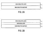
- FIG. 2Ais a cross-sectional view of a high-K metal oxide dielectric layer formed directly on a substrate prior to undergoing a buffered anneal process.
- FIG. 2Bis a cross-sectional view of a substrate, interfacial layer, and high-K metal oxide dielectric layer prior to undergoing a buffered anneal process.
- FIG. 3is a graph illustrating the thermodynamic chemical equilibrium of Al 2 O 3 and the thermodynamic chemical equilibrium between SiO and SiO 2 .
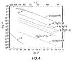
- FIG. 4is a graph illustrating P O2 (partial pressure of oxygen) values achievable, as a function of temperature, for various buffered gas mixtures.
- FIG. 5is a cross-sectional view of a transistor structure constructed in accordance with the present invention.
- the present inventionprovides a method of fabricating a semiconductor device having a metal oxide dielectric layer with a high dielectric constant (high-K), annealed with a buffered anneal process.
- An interfacial layersuch as SiO 2 is optionally present between the metal oxide layer and substrate during the buffered anneal process.
- the buffered anneal processanneals the metal oxide dielectric layer in an oxygen atmosphere in which the partial pressure of oxygen is controlled as a function of anneal temperature such that annealing occurs under conditions at or below the thermodynamic chemical equilibrium for SiO/SiO 2 and at or above the thermodynamic chemical equilibrium for the metal oxide dielectric layer.
- a high-K gate dielectricis one that has a dielectric constant greater than 3.9 (i.e., the dielectric constant of SiO 2 ).
- Annealingis a general term that means thermal treatment to alleviate some condition such as stress, phase separation, or deviation from stoichiometry.
- a buffered anneal processis an anneal process carried out in a buffered atmosphere, such as an atmosphere in which the partial pressure of a gaseous element is controlled by the chemical equilibrium between two other gases.
- the P O2partial pressure of oxygen
- a dielectric layer 1is formed over a semiconductor substrate surface 3 as shown in FIG. 2 A.
- the dielectric layer 1is a high-K metal oxide dielectric layer.
- the substrate 3may be a silicon substrate.
- Conventional methods and techniquesare used to form the high-K metal oxide dielectric layer 1 such as atomic layer deposition (ALD), chemical vapor deposition (CVD), molecular beam epitaxy (MBE), reactive sputtering, evaporation, and other processes well-known in the art.
- Al 2 O 3(aluminum oxide) is the metal oxide used in the following description of the invention. It should be appreciated, however, that other high-K metal oxide dielectrics such as unary oxides ZrO 2 , HfO 2 , TiO 2 , and Ta 2 O 5 can also be used. For instance, Al 2 O 3 has a dielectric constant of approximately 9 to approximately 10; whereas TiO 2 has a dielectric constant from approximately 80 to approximately 110.
- unary oxidescan combine with other unary oxides to form binary oxides such as Zr x Ti y O z , BaTiO 3 , and SrTiO 3 . Ternary and higher order metal oxides are also contemplated.
- Combinations of unary, binary, or ternary oxides with SiO 2 (i.e., silicate formation) or Al 2 O 3 (i.e., aluminate formation)can also be used in forming the high-K metal oxide dielectric layer.
- metal silicate high-K materialsinclude ZrSiO 4 and HfSiO 4 .
- aluminate high-K materialsinclude Zr x Al y O z and Hf x Al y O z .
- An interfacial layer 2can be optionally provided between the semiconductor substrate 3 and the high-K metal oxide dielectric layer 1 as shown in FIG. 2 B.
- the interfacial layer 2is a minimally thin layer of SiO 2 , silicon oxynitride (Si—O—N), or chemically-prepared silicon oxide (Si—O—H) and is provided as an interfacial layer 2 between the deposited high-K metal oxide dielectric layer 1 and the underlying silicon substrate 3 through conventional methods and techniques.
- the interfacial layer 2is a dielectric layer providing a good electrical interface between the high-K metal oxide dielectric layer 1 and the substrate 3 .
- the interfacial layer 2can also facilitate fabrication of the high-K metal oxide dielectric layer 1 .
- the interfacial layer 2can be formed prior to, simultaneously, with, or even after formation of the high-K metal oxide dielectric layer 1 .
- the fabrication conditions for forming a metal oxide directly on substrate 3can result in the contemporaneous formation of the interfacial layer 2 .
- a deposition chamber used for growth of a metal oxidemay contain water vapor or O 2 which results in oxidation of the underlying silicon substrate 3 and contemporaneous formation of the interfacial layer 2 with the formation of the high-K metal oxide dielectric layer 1 .
- Subsequent formation of the interfacial layer 2occurs when the high-K metal oxide dielectric layer 1 is formed using a clean technique such as MBE.
- the interfacial layer 2is then formed underneath the high-K metal oxide dielectric layer 1 in any subsequent reoxidation step.
- an optional interfacial layer 2which is formed prior to the formation of the high-K metal oxide dielectric layer 1 as an SiO 2 interfacial layer 2 .
- silicon oxynitride or a chemically-prepared silicon oxide (Si—O—H)may also be used as the interfacial layer 2 .
- the exemplary Al 2 O 3 dielectric layeris thus formed over the SiO 2 , silicon oxynitride, or a chemically-prepared silicon oxide optional interfacial layer.
- FIG. 3is a graph illustrating the parameters for the buffered annealing of the high-K Al 2 O 3 dielectric layer under conditions where the partial pressures of oxygen are controlled.
- line 10illustrates the SiO/SiO 2 (silicon oxide/silicon dioxide) thermodynamic chemical equilibrium at different temperatures.
- Line 10is well-known in the art as Smith and Ghidini, and Morrison and Lander lines. See F. W. Smith and G. Ghidini, “ Reaction of Oxygen with Si (111) and (100): Critical Conditions for the Growth of SiO 2 ”, J. Electrochem. Soc., 129, p. 1300 (1982); J. J. Lander and J. Morrison, J. App. Phys., 33, p. 2089 (1962).
- Line 20 of FIG. 3illustrates a similar thermodynamic chemical equilibrium line for Al 2 O 3 . Other similar thermodynamic chemical equilibrium lines 20 exist for other metal oxides.
- the present inventionanneals the high-K metal oxide dielectric layer (here Al 2 O 3 ) under conditions that occur at or between line 10 , for the SiO/SiO 2 thermodynamic chemical equilibrium, and line 20 , for the metal oxide thermodynamic chemical equilibrium (here the thermodynamic chemical equilibrium for Al 2 O 3 ). Therefore,) the embodiment of the present invention uses a buffered anneal process that occurs under conditions between the SiO/SiO 2 thermodynamic chemical equilibrium line 10 , as depicted in FIG. 3, and the M x O y thermodynamic chemical equilibrium line 20 of FIG. 3, where M is any metal utilized in forming the high-K metal oxide dielectric layer. As noted, Al 2 O 3 is utilized as an exemplary M x O y throughout the detailed description.
- the buffered anneal processcan also be applied to binary, ternary, and other multi-component oxides.
- the buffered anneal processis conducted by controlling the partial pressure of oxygen (P O2 ) at a given anneal temperature (i.e., at different temperature regimes).
- P O2partial pressure of oxygen
- the buffered annealcan be carried out under conditions where the P O2 can range from approximately 10 Torr to approximately 10 ⁇ 40 Torr with anneal process temperatures ranging from approximately 400° C. to approximately 1200° C. as shown in FIG. 3 .
- a certain desired P O2is achieved by selecting the buffered environment.
- the selected P O2is achieved by controlling the gas flow ratio of buffered gases at a given anneal temperature, or by direct oxygen flow at a given anneal temperature.
- the P O2can be controlled by direct control of O 2 flow where the desired P O2 is greater than or equal to 10 ⁇ 2 Torr.
- the P O2is controlled by direct O 2 flow only for large P O2 . For instance, where partial pressures are approximately or greater than 10 ⁇ 2 Torr.
- Lower values of the P O2can be controlled by the flow rate ratio of gases such as CO 2 /CO (lines 30 , 40 , 50 , 60 , 70 ) or H 2 O/H 2 (line 80 ) as shown in FIG. 4 .
- gasessuch as CO 2 /CO (lines 30 , 40 , 50 , 60 , 70 ) or H 2 O/H 2 (line 80 ) as shown in FIG. 4 .
- the gas mixtures illustrated in FIG. 4are known as buffered gas mixtures.
- the present inventioncontrols the P O2 over a very large range when controlling the CO 2 /CO (lines 30 , 40 , 50 , 60 , 70 ) or H 2 O/H 2 (line 80 ) gas flow ratios.
- Line 30illustrates a CO 2 /CO ratio of 106 .
- Line 40illustrates a CO 2 /CO ratio of 10 ⁇ 6 .
- Line 50illustrates a CO 2 /CO ratio of 10 3 .
- Line 60illustrates a CO 2 /CO ratio of 10 .
- Line 70illustrates a CO 2 /CO ratio of 10 ⁇ 1 .
- Line 80illustrates an H 2 O/H, ratio of 10. Additional ratios of CO 2 /CO mixtures or H 2 O/H 2 mixtures as a function of temperature could easily be used to affect the P O2 depending upon the desired buffered annealing environment.
- FIG. 4illustrates examples of the various P O2 values achievable through different buffered gas mixtures at particular temperatures; other values could easily be illustrated.
- the high-K metal oxide dielectric layerundergoes a buffered anneal process utilizing a buffered gas mixture of CO 2 /CO rather than H 2 O/H 2 .
- the inventioncan also provide a reduction in the fixed charge of the high-K metal oxide dielectric layer by providing a more stoichiometric metal oxide layer.
- Stoichiometry of the metal oxide layercan be influenced by the value of P O2 used during an anneal. As a result, selecting a certain buffered anneal environment at a given anneal temperature, can enable one to exert control over and affect the overall metal oxide stoichiometry and its fixed charge.
- the high-K metal oxide dielectric layeris annealed under conditions which are below the SiO/SiO 2 thermodynamic chemical equilibrium line 10 and closer to the thermodynamic chemical equilibrium line of the metal oxide (i.e., closer to line 20 of FIG. 3 for Al 2 O 3 ), a more stoichiometric metal oxide dielectric layer is produced having a reduced fixed net charge.
- the closer the anneal conditions are for the thermodynamic chemical equilibrium of the metal oxide dielectric layeri.e., line 20 for Al 2 O 3
- the net fixed charge of the metal oxide dielectric layerthe closer the anneal conditions are for the thermodynamic chemical equilibrium of the metal oxide dielectric layer (i.e., line 20 for Al 2 O 3 ) the lower the net fixed charge of the metal oxide dielectric layer.
- FIGS. 1 and 3graphically illustrate in a P O2 and temperature regime, the stable SiO 2 regime which is found at and above line 10 .
- siliconreacts in the presence of oxygen and preferentially forms SiO 2 .
- FIGS. 1 and 3also illustrate the unstable SiO 2 regime which occurs below line 10 where silicon reacts in the presence of oxygen and forms SiO; a volatile compound.
- SiO 2is completely stable and minimum reoxidation results when the anneal occurs at or near the SiO/SiO 2 thermodynamic chemical equilibrium line 10 .
- thermodynamic chemical equilibrium line 10for SiO/SiO 2 .
- Buffered annealing conditionswhere the P O2 and temperature are selected close to or at the SiO 2 thermodynamic chemical equilibrium line 10 , provides for minimal disruption of the Si/SiO 2 interface. Specifically, below the thermodynamic chemical equilibrium line 10 there is no silicon dioxide growth at the existing interfacial layer.
- thermodynamic chemical equilibrium line 10At or slightly above the thermodynamic chemical equilibrium line 10 , approximately zero A° to approximately 2 A° of silicon dioxide is added to the interfacial layer as a result of the buffered anneal process when the process is carried out close to but below the thermodynamic chemical equilibrium line 10 .
- the inventionprovides wide latitude for annealing the high-K metal oxide dielectric layer, it is preferably annealed with a P O2 in a range of approximately 10 Torr to approximately 10 ⁇ 20 Torr, and at a temperature ranging from approximately 400° C. to approximately 1200° C.
- the annealresults in the SiO 2 layer (i.e., interfacial layer) decomposing into SiO.
- the SiO 2 layeri.e., interfacial layer
- decomposition of SiO 2is undesirable.
- decomposition of SiO 2can be desirable.
- Silicate formationoccurs by a reaction between the SiO 2 layer (i.e., interfacial layer) and the metal oxide dielectric layer.
- portions of the decomposing SiO 2 layeri.e., SiO
- react with the high-K gate dielectric layerforming a silicate structure.
- the resulting silicate structuremay be desirable since silicates are viable high-K gate structures with dielectric constants greater than 3.9 (i.e., greater than the dielectric constant of silicon dioxide).
- the buffered anneal process of the inventioncan also be carried out in multiple steps.
- a high-K metal oxide dielectric layer 1is provided as a first layer directly over the substrate 3
- this layercan first be annealed in a buffered environment containing oxygen which occurs at or near the thermodynamic chemical equilibrium line of the metal oxide dielectric layer (i.e., line 20 of FIG. 3 for Al 2 O 3 ) bringing the metal oxide to near or at its stoichiometric point.
- An interfacial layer 2may then be created after the first anneal is completed.
- the interfacial layer 2if already present to some degree, can be reoxidized as desired to enhance the interfacial region.
- the high-K metal oxide dielectric layer 1 , the interfacial layer 2 , and substrate 3are then annealed in a buffered atmosphere containing oxygen in a second buffered anneal.
- the second buffered annealis carried out under conditions at or very close to the thermodynamic chemical equilibrium line of SiO/SiO 2 , that is, line 10 in FIGS. 1 and 3.
- the second buffered annealis preferably not carried out under conditions existing below line 10 as SiO 2 would not reoxidize, but decompose into SiO.
- a high-K metal oxide dielectricis formed that has a fixed charge of greater than approximately 10 10 /cm 2 and less than approximately 10 12 /cm 2 .
- the interfacial layer 2if present during the buffered anneal, increases in thickness by approximately zero A° to approximately 2 A° resulting in substantially less reoxidation of the interfacial layer 2 .
- the buffer annealed metal oxide dielectric layer 1produced in accordance with the invention, can be used as a gate oxide with a gate conductor 4 provided on top of the gate oxide layer in a transistor, as shown in FIG. 5, or in other semiconductor structures such as a dielectric layer in a capacitor.
Landscapes
- Engineering & Computer Science (AREA)
- Microelectronics & Electronic Packaging (AREA)
- Condensed Matter Physics & Semiconductors (AREA)
- General Physics & Mathematics (AREA)
- Manufacturing & Machinery (AREA)
- Computer Hardware Design (AREA)
- Physics & Mathematics (AREA)
- Power Engineering (AREA)
- Chemical & Material Sciences (AREA)
- Chemical Kinetics & Catalysis (AREA)
- Crystallography & Structural Chemistry (AREA)
- General Chemical & Material Sciences (AREA)
- Formation Of Insulating Films (AREA)
- Insulated Gate Type Field-Effect Transistor (AREA)
Abstract
Description
Claims (18)
Priority Applications (2)
| Application Number | Priority Date | Filing Date | Title |
|---|---|---|---|
| US10/151,887US6797525B2 (en) | 2002-05-22 | 2002-05-22 | Fabrication process for a semiconductor device having a metal oxide dielectric material with a high dielectric constant, annealed with a buffered anneal process |
| US10/947,218US20050042846A1 (en) | 2002-05-22 | 2004-09-23 | Fabrication process for a semiconductor device having a metal oxide dielectric material with a high dielectric constant, annealed with a buffered anneal process |
Applications Claiming Priority (1)
| Application Number | Priority Date | Filing Date | Title |
|---|---|---|---|
| US10/151,887US6797525B2 (en) | 2002-05-22 | 2002-05-22 | Fabrication process for a semiconductor device having a metal oxide dielectric material with a high dielectric constant, annealed with a buffered anneal process |
Related Child Applications (1)
| Application Number | Title | Priority Date | Filing Date |
|---|---|---|---|
| US10/947,218DivisionUS20050042846A1 (en) | 2002-05-22 | 2004-09-23 | Fabrication process for a semiconductor device having a metal oxide dielectric material with a high dielectric constant, annealed with a buffered anneal process |
Publications (2)
| Publication Number | Publication Date |
|---|---|
| US20030219972A1 US20030219972A1 (en) | 2003-11-27 |
| US6797525B2true US6797525B2 (en) | 2004-09-28 |
Family
ID=29548405
Family Applications (2)
| Application Number | Title | Priority Date | Filing Date |
|---|---|---|---|
| US10/151,887Expired - LifetimeUS6797525B2 (en) | 2002-05-22 | 2002-05-22 | Fabrication process for a semiconductor device having a metal oxide dielectric material with a high dielectric constant, annealed with a buffered anneal process |
| US10/947,218AbandonedUS20050042846A1 (en) | 2002-05-22 | 2004-09-23 | Fabrication process for a semiconductor device having a metal oxide dielectric material with a high dielectric constant, annealed with a buffered anneal process |
Family Applications After (1)
| Application Number | Title | Priority Date | Filing Date |
|---|---|---|---|
| US10/947,218AbandonedUS20050042846A1 (en) | 2002-05-22 | 2004-09-23 | Fabrication process for a semiconductor device having a metal oxide dielectric material with a high dielectric constant, annealed with a buffered anneal process |
Country Status (1)
| Country | Link |
|---|---|
| US (2) | US6797525B2 (en) |
Cited By (12)
| Publication number | Priority date | Publication date | Assignee | Title |
|---|---|---|---|---|
| US20020090777A1 (en)* | 2001-01-05 | 2002-07-11 | Leonard Forbes | Methods of forming capacitor structures, and capacitor structures |
| US20030017715A1 (en)* | 2001-02-01 | 2003-01-23 | Muller David A. | Composite gate dielectric layer |
| US20050059259A1 (en)* | 2003-09-16 | 2005-03-17 | Tokyo Electron Limited | Interfacial oxidation process for high-k gate dielectric process integration |
| US20050151184A1 (en)* | 2001-02-02 | 2005-07-14 | Lee Jong-Ho | Dielectric layer for semiconductor device and method of manufacturing the same |
| US20060081905A1 (en)* | 2004-10-15 | 2006-04-20 | Samsung Electronics Co., Ltd. | Dielectric multilayer of microelectronic device and method of fabricating the same |
| US20060097305A1 (en)* | 2004-11-08 | 2006-05-11 | Lee Kee-Jeung | Capacitor with zirconium oxide and method for fabricating the same |
| US20060237803A1 (en)* | 2005-04-21 | 2006-10-26 | International Business Machines Corporation | ULTRA-THIN Hf-DOPED-SILICON OXYNITRIDE FILM FOR HIGH PERFORMANCE CMOS APPLICATIONS AND METHOD OF MANUFACTURE |
| US20070001201A1 (en)* | 2005-06-30 | 2007-01-04 | Deok-Sin Kil | Capacitor with nano-composite dielectric layer and method for fabricating the same |
| US20070051998A1 (en)* | 2005-09-08 | 2007-03-08 | Deok-Sin Kil | Semiconductor memory device with dielectric structure and method for fabricating the same |
| US20080138503A1 (en)* | 2004-12-23 | 2008-06-12 | Hynix Semiconductor Inc. | Method For Forming Dielectric Film And Method For Forming Capacitor In Semiconductor Device Using The Same |
| US7825043B2 (en) | 2005-11-28 | 2010-11-02 | Hynix Semiconductor Inc. | Method for fabricating capacitor in semiconductor device |
| US20130034940A1 (en)* | 2009-06-18 | 2013-02-07 | International Business Machines Corporation | Low Threshold Voltage And Inversion Oxide thickness Scaling For A High-K Metal Gate P-Type MOSFET |
Families Citing this family (366)
| Publication number | Priority date | Publication date | Assignee | Title |
|---|---|---|---|---|
| WO2004008544A1 (en)* | 2002-07-16 | 2004-01-22 | Nec Corporation | Semiconductor device, production method and production device thereof |
| JP3974547B2 (en)* | 2003-03-31 | 2007-09-12 | 株式会社東芝 | Semiconductor device and manufacturing method of semiconductor device |
| US20070023842A1 (en)* | 2003-11-12 | 2007-02-01 | Hyung-Suk Jung | Semiconductor devices having different gate dielectric layers and methods of manufacturing the same |
| TWI258811B (en)* | 2003-11-12 | 2006-07-21 | Samsung Electronics Co Ltd | Semiconductor devices having different gate dielectrics and methods for manufacturing the same |
| US20050224897A1 (en)* | 2004-03-26 | 2005-10-13 | Taiwan Semiconductor Manufacturing Co., Ltd. | High-K gate dielectric stack with buffer layer to improve threshold voltage characteristics |
| US20060151846A1 (en)* | 2005-01-13 | 2006-07-13 | International Business Machines Corporation | Method of forming HfSiN metal for n-FET applications |
| JP4522900B2 (en)* | 2005-03-30 | 2010-08-11 | 東京エレクトロン株式会社 | Film forming method and recording medium |
| US20090087623A1 (en)* | 2007-09-28 | 2009-04-02 | Brazier Mark R | Methods for the deposition of ternary oxide gate dielectrics and structures formed thereby |
| US10378106B2 (en) | 2008-11-14 | 2019-08-13 | Asm Ip Holding B.V. | Method of forming insulation film by modified PEALD |
| US9394608B2 (en) | 2009-04-06 | 2016-07-19 | Asm America, Inc. | Semiconductor processing reactor and components thereof |
| US8895352B2 (en)* | 2009-06-02 | 2014-11-25 | International Business Machines Corporation | Method to improve nucleation of materials on graphene and carbon nanotubes |
| US8268683B2 (en)* | 2009-06-12 | 2012-09-18 | Taiwan Semiconductor Manufacturing Company, Ltd. | Method for reducing interfacial layer thickness for high-K and metal gate stack |
| US8802201B2 (en) | 2009-08-14 | 2014-08-12 | Asm America, Inc. | Systems and methods for thin-film deposition of metal oxides using excited nitrogen-oxygen species |
| US8350341B2 (en)* | 2010-04-09 | 2013-01-08 | International Business Machines Corporation | Method and structure for work function engineering in transistors including a high dielectric constant gate insulator and metal gate (HKMG) |
| US9312155B2 (en) | 2011-06-06 | 2016-04-12 | Asm Japan K.K. | High-throughput semiconductor-processing apparatus equipped with multiple dual-chamber modules |
| US10364496B2 (en) | 2011-06-27 | 2019-07-30 | Asm Ip Holding B.V. | Dual section module having shared and unshared mass flow controllers |
| US10854498B2 (en) | 2011-07-15 | 2020-12-01 | Asm Ip Holding B.V. | Wafer-supporting device and method for producing same |
| US20130023129A1 (en) | 2011-07-20 | 2013-01-24 | Asm America, Inc. | Pressure transmitter for a semiconductor processing environment |
| US9017481B1 (en) | 2011-10-28 | 2015-04-28 | Asm America, Inc. | Process feed management for semiconductor substrate processing |
| US9659799B2 (en) | 2012-08-28 | 2017-05-23 | Asm Ip Holding B.V. | Systems and methods for dynamic semiconductor process scheduling |
| US10714315B2 (en) | 2012-10-12 | 2020-07-14 | Asm Ip Holdings B.V. | Semiconductor reaction chamber showerhead |
| US20160376700A1 (en) | 2013-02-01 | 2016-12-29 | Asm Ip Holding B.V. | System for treatment of deposition reactor |
| US9589770B2 (en) | 2013-03-08 | 2017-03-07 | Asm Ip Holding B.V. | Method and systems for in-situ formation of intermediate reactive species |
| US9484191B2 (en) | 2013-03-08 | 2016-11-01 | Asm Ip Holding B.V. | Pulsed remote plasma method and system |
| US8993054B2 (en)* | 2013-07-12 | 2015-03-31 | Asm Ip Holding B.V. | Method and system to reduce outgassing in a reaction chamber |
| US9240412B2 (en) | 2013-09-27 | 2016-01-19 | Asm Ip Holding B.V. | Semiconductor structure and device and methods of forming same using selective epitaxial process |
| US10683571B2 (en) | 2014-02-25 | 2020-06-16 | Asm Ip Holding B.V. | Gas supply manifold and method of supplying gases to chamber using same |
| US10167557B2 (en) | 2014-03-18 | 2019-01-01 | Asm Ip Holding B.V. | Gas distribution system, reactor including the system, and methods of using the same |
| US11015245B2 (en) | 2014-03-19 | 2021-05-25 | Asm Ip Holding B.V. | Gas-phase reactor and system having exhaust plenum and components thereof |
| US10858737B2 (en) | 2014-07-28 | 2020-12-08 | Asm Ip Holding B.V. | Showerhead assembly and components thereof |
| US9890456B2 (en) | 2014-08-21 | 2018-02-13 | Asm Ip Holding B.V. | Method and system for in situ formation of gas-phase compounds |
| JP2016066641A (en)* | 2014-09-22 | 2016-04-28 | 株式会社東芝 | Semiconductor device and method of manufacturing the same |
| US10941490B2 (en) | 2014-10-07 | 2021-03-09 | Asm Ip Holding B.V. | Multiple temperature range susceptor, assembly, reactor and system including the susceptor, and methods of using the same |
| US9657845B2 (en) | 2014-10-07 | 2017-05-23 | Asm Ip Holding B.V. | Variable conductance gas distribution apparatus and method |
| KR102263121B1 (en) | 2014-12-22 | 2021-06-09 | 에이에스엠 아이피 홀딩 비.브이. | Semiconductor device and manufacuring method thereof |
| US10529542B2 (en) | 2015-03-11 | 2020-01-07 | Asm Ip Holdings B.V. | Cross-flow reactor and method |
| US10276355B2 (en) | 2015-03-12 | 2019-04-30 | Asm Ip Holding B.V. | Multi-zone reactor, system including the reactor, and method of using the same |
| US10458018B2 (en) | 2015-06-26 | 2019-10-29 | Asm Ip Holding B.V. | Structures including metal carbide material, devices including the structures, and methods of forming same |
| US10600673B2 (en) | 2015-07-07 | 2020-03-24 | Asm Ip Holding B.V. | Magnetic susceptor to baseplate seal |
| US9960072B2 (en) | 2015-09-29 | 2018-05-01 | Asm Ip Holding B.V. | Variable adjustment for precise matching of multiple chamber cavity housings |
| US10211308B2 (en) | 2015-10-21 | 2019-02-19 | Asm Ip Holding B.V. | NbMC layers |
| US10322384B2 (en) | 2015-11-09 | 2019-06-18 | Asm Ip Holding B.V. | Counter flow mixer for process chamber |
| CN106847696B (en)* | 2015-12-07 | 2020-05-08 | 中芯国际集成电路制造(上海)有限公司 | Method for forming fin field effect transistor |
| CN106847893B (en)* | 2015-12-07 | 2020-05-08 | 中芯国际集成电路制造(上海)有限公司 | Method of forming a fin field effect transistor |
| US11139308B2 (en) | 2015-12-29 | 2021-10-05 | Asm Ip Holding B.V. | Atomic layer deposition of III-V compounds to form V-NAND devices |
| US10529554B2 (en) | 2016-02-19 | 2020-01-07 | Asm Ip Holding B.V. | Method for forming silicon nitride film selectively on sidewalls or flat surfaces of trenches |
| US10468251B2 (en) | 2016-02-19 | 2019-11-05 | Asm Ip Holding B.V. | Method for forming spacers using silicon nitride film for spacer-defined multiple patterning |
| US10501866B2 (en) | 2016-03-09 | 2019-12-10 | Asm Ip Holding B.V. | Gas distribution apparatus for improved film uniformity in an epitaxial system |
| US10343920B2 (en) | 2016-03-18 | 2019-07-09 | Asm Ip Holding B.V. | Aligned carbon nanotubes |
| US9892913B2 (en) | 2016-03-24 | 2018-02-13 | Asm Ip Holding B.V. | Radial and thickness control via biased multi-port injection settings |
| US10865475B2 (en) | 2016-04-21 | 2020-12-15 | Asm Ip Holding B.V. | Deposition of metal borides and silicides |
| US10190213B2 (en) | 2016-04-21 | 2019-01-29 | Asm Ip Holding B.V. | Deposition of metal borides |
| US10032628B2 (en) | 2016-05-02 | 2018-07-24 | Asm Ip Holding B.V. | Source/drain performance through conformal solid state doping |
| US10367080B2 (en) | 2016-05-02 | 2019-07-30 | Asm Ip Holding B.V. | Method of forming a germanium oxynitride film |
| KR102592471B1 (en) | 2016-05-17 | 2023-10-20 | 에이에스엠 아이피 홀딩 비.브이. | Method of forming metal interconnection and method of fabricating semiconductor device using the same |
| US11453943B2 (en) | 2016-05-25 | 2022-09-27 | Asm Ip Holding B.V. | Method for forming carbon-containing silicon/metal oxide or nitride film by ALD using silicon precursor and hydrocarbon precursor |
| US10388509B2 (en) | 2016-06-28 | 2019-08-20 | Asm Ip Holding B.V. | Formation of epitaxial layers via dislocation filtering |
| US9859151B1 (en) | 2016-07-08 | 2018-01-02 | Asm Ip Holding B.V. | Selective film deposition method to form air gaps |
| US10612137B2 (en) | 2016-07-08 | 2020-04-07 | Asm Ip Holdings B.V. | Organic reactants for atomic layer deposition |
| US10714385B2 (en) | 2016-07-19 | 2020-07-14 | Asm Ip Holding B.V. | Selective deposition of tungsten |
| KR102354490B1 (en) | 2016-07-27 | 2022-01-21 | 에이에스엠 아이피 홀딩 비.브이. | Method of processing a substrate |
| US9887082B1 (en) | 2016-07-28 | 2018-02-06 | Asm Ip Holding B.V. | Method and apparatus for filling a gap |
| US10395919B2 (en) | 2016-07-28 | 2019-08-27 | Asm Ip Holding B.V. | Method and apparatus for filling a gap |
| KR102532607B1 (en) | 2016-07-28 | 2023-05-15 | 에이에스엠 아이피 홀딩 비.브이. | Substrate processing apparatus and method of operating the same |
| US9812320B1 (en) | 2016-07-28 | 2017-11-07 | Asm Ip Holding B.V. | Method and apparatus for filling a gap |
| US10541128B2 (en)* | 2016-08-19 | 2020-01-21 | International Business Machines Corporation | Method for making VFET devices with ILD protection |
| KR102613349B1 (en) | 2016-08-25 | 2023-12-14 | 에이에스엠 아이피 홀딩 비.브이. | Exhaust apparatus and substrate processing apparatus and thin film fabricating method using the same |
| US10410943B2 (en) | 2016-10-13 | 2019-09-10 | Asm Ip Holding B.V. | Method for passivating a surface of a semiconductor and related systems |
| US10643826B2 (en) | 2016-10-26 | 2020-05-05 | Asm Ip Holdings B.V. | Methods for thermally calibrating reaction chambers |
| US11532757B2 (en) | 2016-10-27 | 2022-12-20 | Asm Ip Holding B.V. | Deposition of charge trapping layers |
| US10229833B2 (en) | 2016-11-01 | 2019-03-12 | Asm Ip Holding B.V. | Methods for forming a transition metal nitride film on a substrate by atomic layer deposition and related semiconductor device structures |
| US10643904B2 (en) | 2016-11-01 | 2020-05-05 | Asm Ip Holdings B.V. | Methods for forming a semiconductor device and related semiconductor device structures |
| US10714350B2 (en) | 2016-11-01 | 2020-07-14 | ASM IP Holdings, B.V. | Methods for forming a transition metal niobium nitride film on a substrate by atomic layer deposition and related semiconductor device structures |
| US10435790B2 (en) | 2016-11-01 | 2019-10-08 | Asm Ip Holding B.V. | Method of subatmospheric plasma-enhanced ALD using capacitively coupled electrodes with narrow gap |
| US10134757B2 (en) | 2016-11-07 | 2018-11-20 | Asm Ip Holding B.V. | Method of processing a substrate and a device manufactured by using the method |
| KR102546317B1 (en) | 2016-11-15 | 2023-06-21 | 에이에스엠 아이피 홀딩 비.브이. | Gas supply unit and substrate processing apparatus including the same |
| US10340135B2 (en) | 2016-11-28 | 2019-07-02 | Asm Ip Holding B.V. | Method of topologically restricted plasma-enhanced cyclic deposition of silicon or metal nitride |
| KR102762543B1 (en) | 2016-12-14 | 2025-02-05 | 에이에스엠 아이피 홀딩 비.브이. | Substrate processing apparatus |
| US11447861B2 (en) | 2016-12-15 | 2022-09-20 | Asm Ip Holding B.V. | Sequential infiltration synthesis apparatus and a method of forming a patterned structure |
| US11581186B2 (en) | 2016-12-15 | 2023-02-14 | Asm Ip Holding B.V. | Sequential infiltration synthesis apparatus |
| KR102700194B1 (en) | 2016-12-19 | 2024-08-28 | 에이에스엠 아이피 홀딩 비.브이. | Substrate processing apparatus |
| US10269558B2 (en) | 2016-12-22 | 2019-04-23 | Asm Ip Holding B.V. | Method of forming a structure on a substrate |
| US10867788B2 (en) | 2016-12-28 | 2020-12-15 | Asm Ip Holding B.V. | Method of forming a structure on a substrate |
| US11390950B2 (en) | 2017-01-10 | 2022-07-19 | Asm Ip Holding B.V. | Reactor system and method to reduce residue buildup during a film deposition process |
| US10655221B2 (en) | 2017-02-09 | 2020-05-19 | Asm Ip Holding B.V. | Method for depositing oxide film by thermal ALD and PEALD |
| US10468261B2 (en) | 2017-02-15 | 2019-11-05 | Asm Ip Holding B.V. | Methods for forming a metallic film on a substrate by cyclical deposition and related semiconductor device structures |
| US10529563B2 (en) | 2017-03-29 | 2020-01-07 | Asm Ip Holdings B.V. | Method for forming doped metal oxide films on a substrate by cyclical deposition and related semiconductor device structures |
| US10283353B2 (en) | 2017-03-29 | 2019-05-07 | Asm Ip Holding B.V. | Method of reforming insulating film deposited on substrate with recess pattern |
| KR102457289B1 (en) | 2017-04-25 | 2022-10-21 | 에이에스엠 아이피 홀딩 비.브이. | Method for depositing a thin film and manufacturing a semiconductor device |
| US10892156B2 (en) | 2017-05-08 | 2021-01-12 | Asm Ip Holding B.V. | Methods for forming a silicon nitride film on a substrate and related semiconductor device structures |
| US10446393B2 (en) | 2017-05-08 | 2019-10-15 | Asm Ip Holding B.V. | Methods for forming silicon-containing epitaxial layers and related semiconductor device structures |
| US10770286B2 (en) | 2017-05-08 | 2020-09-08 | Asm Ip Holdings B.V. | Methods for selectively forming a silicon nitride film on a substrate and related semiconductor device structures |
| US10504742B2 (en) | 2017-05-31 | 2019-12-10 | Asm Ip Holding B.V. | Method of atomic layer etching using hydrogen plasma |
| US10886123B2 (en) | 2017-06-02 | 2021-01-05 | Asm Ip Holding B.V. | Methods for forming low temperature semiconductor layers and related semiconductor device structures |
| US12040200B2 (en) | 2017-06-20 | 2024-07-16 | Asm Ip Holding B.V. | Semiconductor processing apparatus and methods for calibrating a semiconductor processing apparatus |
| US11306395B2 (en) | 2017-06-28 | 2022-04-19 | Asm Ip Holding B.V. | Methods for depositing a transition metal nitride film on a substrate by atomic layer deposition and related deposition apparatus |
| US10685834B2 (en) | 2017-07-05 | 2020-06-16 | Asm Ip Holdings B.V. | Methods for forming a silicon germanium tin layer and related semiconductor device structures |
| KR20190009245A (en) | 2017-07-18 | 2019-01-28 | 에이에스엠 아이피 홀딩 비.브이. | Methods for forming a semiconductor device structure and related semiconductor device structures |
| US11018002B2 (en) | 2017-07-19 | 2021-05-25 | Asm Ip Holding B.V. | Method for selectively depositing a Group IV semiconductor and related semiconductor device structures |
| US10541333B2 (en) | 2017-07-19 | 2020-01-21 | Asm Ip Holding B.V. | Method for depositing a group IV semiconductor and related semiconductor device structures |
| US11374112B2 (en) | 2017-07-19 | 2022-06-28 | Asm Ip Holding B.V. | Method for depositing a group IV semiconductor and related semiconductor device structures |
| US10312055B2 (en) | 2017-07-26 | 2019-06-04 | Asm Ip Holding B.V. | Method of depositing film by PEALD using negative bias |
| US10605530B2 (en) | 2017-07-26 | 2020-03-31 | Asm Ip Holding B.V. | Assembly of a liner and a flange for a vertical furnace as well as the liner and the vertical furnace |
| US10590535B2 (en) | 2017-07-26 | 2020-03-17 | Asm Ip Holdings B.V. | Chemical treatment, deposition and/or infiltration apparatus and method for using the same |
| TWI815813B (en) | 2017-08-04 | 2023-09-21 | 荷蘭商Asm智慧財產控股公司 | Showerhead assembly for distributing a gas within a reaction chamber |
| US10770336B2 (en) | 2017-08-08 | 2020-09-08 | Asm Ip Holding B.V. | Substrate lift mechanism and reactor including same |
| US10692741B2 (en) | 2017-08-08 | 2020-06-23 | Asm Ip Holdings B.V. | Radiation shield |
| US11769682B2 (en) | 2017-08-09 | 2023-09-26 | Asm Ip Holding B.V. | Storage apparatus for storing cassettes for substrates and processing apparatus equipped therewith |
| US10249524B2 (en) | 2017-08-09 | 2019-04-02 | Asm Ip Holding B.V. | Cassette holder assembly for a substrate cassette and holding member for use in such assembly |
| US11139191B2 (en) | 2017-08-09 | 2021-10-05 | Asm Ip Holding B.V. | Storage apparatus for storing cassettes for substrates and processing apparatus equipped therewith |
| USD900036S1 (en) | 2017-08-24 | 2020-10-27 | Asm Ip Holding B.V. | Heater electrical connector and adapter |
| US11830730B2 (en) | 2017-08-29 | 2023-11-28 | Asm Ip Holding B.V. | Layer forming method and apparatus |
| US11295980B2 (en) | 2017-08-30 | 2022-04-05 | Asm Ip Holding B.V. | Methods for depositing a molybdenum metal film over a dielectric surface of a substrate by a cyclical deposition process and related semiconductor device structures |
| KR102491945B1 (en) | 2017-08-30 | 2023-01-26 | 에이에스엠 아이피 홀딩 비.브이. | Substrate processing apparatus |
| US11056344B2 (en) | 2017-08-30 | 2021-07-06 | Asm Ip Holding B.V. | Layer forming method |
| KR102401446B1 (en) | 2017-08-31 | 2022-05-24 | 에이에스엠 아이피 홀딩 비.브이. | Substrate processing apparatus |
| US10607895B2 (en) | 2017-09-18 | 2020-03-31 | Asm Ip Holdings B.V. | Method for forming a semiconductor device structure comprising a gate fill metal |
| KR102630301B1 (en) | 2017-09-21 | 2024-01-29 | 에이에스엠 아이피 홀딩 비.브이. | Method of sequential infiltration synthesis treatment of infiltrateable material and structures and devices formed using same |
| US10844484B2 (en) | 2017-09-22 | 2020-11-24 | Asm Ip Holding B.V. | Apparatus for dispensing a vapor phase reactant to a reaction chamber and related methods |
| US10658205B2 (en) | 2017-09-28 | 2020-05-19 | Asm Ip Holdings B.V. | Chemical dispensing apparatus and methods for dispensing a chemical to a reaction chamber |
| US10403504B2 (en) | 2017-10-05 | 2019-09-03 | Asm Ip Holding B.V. | Method for selectively depositing a metallic film on a substrate |
| US10319588B2 (en) | 2017-10-10 | 2019-06-11 | Asm Ip Holding B.V. | Method for depositing a metal chalcogenide on a substrate by cyclical deposition |
| US10923344B2 (en) | 2017-10-30 | 2021-02-16 | Asm Ip Holding B.V. | Methods for forming a semiconductor structure and related semiconductor structures |
| KR102443047B1 (en) | 2017-11-16 | 2022-09-14 | 에이에스엠 아이피 홀딩 비.브이. | Method of processing a substrate and a device manufactured by the same |
| US10910262B2 (en) | 2017-11-16 | 2021-02-02 | Asm Ip Holding B.V. | Method of selectively depositing a capping layer structure on a semiconductor device structure |
| US11022879B2 (en) | 2017-11-24 | 2021-06-01 | Asm Ip Holding B.V. | Method of forming an enhanced unexposed photoresist layer |
| WO2019103613A1 (en) | 2017-11-27 | 2019-05-31 | Asm Ip Holding B.V. | A storage device for storing wafer cassettes for use with a batch furnace |
| CN111344522B (en) | 2017-11-27 | 2022-04-12 | 阿斯莫Ip控股公司 | Including clean mini-environment device |
| US10290508B1 (en) | 2017-12-05 | 2019-05-14 | Asm Ip Holding B.V. | Method for forming vertical spacers for spacer-defined patterning |
| US10872771B2 (en) | 2018-01-16 | 2020-12-22 | Asm Ip Holding B. V. | Method for depositing a material film on a substrate within a reaction chamber by a cyclical deposition process and related device structures |
| TWI799494B (en) | 2018-01-19 | 2023-04-21 | 荷蘭商Asm 智慧財產控股公司 | Deposition method |
| KR102695659B1 (en) | 2018-01-19 | 2024-08-14 | 에이에스엠 아이피 홀딩 비.브이. | Method for depositing a gap filling layer by plasma assisted deposition |
| USD903477S1 (en) | 2018-01-24 | 2020-12-01 | Asm Ip Holdings B.V. | Metal clamp |
| US11018047B2 (en) | 2018-01-25 | 2021-05-25 | Asm Ip Holding B.V. | Hybrid lift pin |
| USD880437S1 (en) | 2018-02-01 | 2020-04-07 | Asm Ip Holding B.V. | Gas supply plate for semiconductor manufacturing apparatus |
| US10535516B2 (en) | 2018-02-01 | 2020-01-14 | Asm Ip Holdings B.V. | Method for depositing a semiconductor structure on a surface of a substrate and related semiconductor structures |
| US11081345B2 (en) | 2018-02-06 | 2021-08-03 | Asm Ip Holding B.V. | Method of post-deposition treatment for silicon oxide film |
| US10896820B2 (en) | 2018-02-14 | 2021-01-19 | Asm Ip Holding B.V. | Method for depositing a ruthenium-containing film on a substrate by a cyclical deposition process |
| WO2019158960A1 (en) | 2018-02-14 | 2019-08-22 | Asm Ip Holding B.V. | A method for depositing a ruthenium-containing film on a substrate by a cyclical deposition process |
| US10731249B2 (en) | 2018-02-15 | 2020-08-04 | Asm Ip Holding B.V. | Method of forming a transition metal containing film on a substrate by a cyclical deposition process, a method for supplying a transition metal halide compound to a reaction chamber, and related vapor deposition apparatus |
| KR102636427B1 (en) | 2018-02-20 | 2024-02-13 | 에이에스엠 아이피 홀딩 비.브이. | Substrate processing method and apparatus |
| US10658181B2 (en) | 2018-02-20 | 2020-05-19 | Asm Ip Holding B.V. | Method of spacer-defined direct patterning in semiconductor fabrication |
| US10975470B2 (en) | 2018-02-23 | 2021-04-13 | Asm Ip Holding B.V. | Apparatus for detecting or monitoring for a chemical precursor in a high temperature environment |
| US11473195B2 (en) | 2018-03-01 | 2022-10-18 | Asm Ip Holding B.V. | Semiconductor processing apparatus and a method for processing a substrate |
| US11629406B2 (en) | 2018-03-09 | 2023-04-18 | Asm Ip Holding B.V. | Semiconductor processing apparatus comprising one or more pyrometers for measuring a temperature of a substrate during transfer of the substrate |
| US11114283B2 (en) | 2018-03-16 | 2021-09-07 | Asm Ip Holding B.V. | Reactor, system including the reactor, and methods of manufacturing and using same |
| KR102646467B1 (en) | 2018-03-27 | 2024-03-11 | 에이에스엠 아이피 홀딩 비.브이. | Method of forming an electrode on a substrate and a semiconductor device structure including an electrode |
| US10510536B2 (en) | 2018-03-29 | 2019-12-17 | Asm Ip Holding B.V. | Method of depositing a co-doped polysilicon film on a surface of a substrate within a reaction chamber |
| US11230766B2 (en) | 2018-03-29 | 2022-01-25 | Asm Ip Holding B.V. | Substrate processing apparatus and method |
| US11088002B2 (en) | 2018-03-29 | 2021-08-10 | Asm Ip Holding B.V. | Substrate rack and a substrate processing system and method |
| KR102501472B1 (en) | 2018-03-30 | 2023-02-20 | 에이에스엠 아이피 홀딩 비.브이. | Substrate processing method |
| KR102600229B1 (en) | 2018-04-09 | 2023-11-10 | 에이에스엠 아이피 홀딩 비.브이. | Substrate supporting device, substrate processing apparatus including the same and substrate processing method |
| US12025484B2 (en) | 2018-05-08 | 2024-07-02 | Asm Ip Holding B.V. | Thin film forming method |
| TWI811348B (en) | 2018-05-08 | 2023-08-11 | 荷蘭商Asm 智慧財產控股公司 | Methods for depositing an oxide film on a substrate by a cyclical deposition process and related device structures |
| US12272527B2 (en) | 2018-05-09 | 2025-04-08 | Asm Ip Holding B.V. | Apparatus for use with hydrogen radicals and method of using same |
| KR20190129718A (en) | 2018-05-11 | 2019-11-20 | 에이에스엠 아이피 홀딩 비.브이. | Methods for forming a doped metal carbide film on a substrate and related semiconductor device structures |
| KR102596988B1 (en) | 2018-05-28 | 2023-10-31 | 에이에스엠 아이피 홀딩 비.브이. | Method of processing a substrate and a device manufactured by the same |
| US11718913B2 (en) | 2018-06-04 | 2023-08-08 | Asm Ip Holding B.V. | Gas distribution system and reactor system including same |
| TWI840362B (en) | 2018-06-04 | 2024-05-01 | 荷蘭商Asm Ip私人控股有限公司 | Wafer handling chamber with moisture reduction |
| US11286562B2 (en) | 2018-06-08 | 2022-03-29 | Asm Ip Holding B.V. | Gas-phase chemical reactor and method of using same |
| KR102568797B1 (en) | 2018-06-21 | 2023-08-21 | 에이에스엠 아이피 홀딩 비.브이. | Substrate processing system |
| US10797133B2 (en) | 2018-06-21 | 2020-10-06 | Asm Ip Holding B.V. | Method for depositing a phosphorus doped silicon arsenide film and related semiconductor device structures |
| TWI873894B (en) | 2018-06-27 | 2025-02-21 | 荷蘭商Asm Ip私人控股有限公司 | Cyclic deposition methods for forming metal-containing material and films and structures including the metal-containing material |
| KR102854019B1 (en) | 2018-06-27 | 2025-09-02 | 에이에스엠 아이피 홀딩 비.브이. | Periodic deposition method for forming a metal-containing material and films and structures comprising the metal-containing material |
| US10612136B2 (en) | 2018-06-29 | 2020-04-07 | ASM IP Holding, B.V. | Temperature-controlled flange and reactor system including same |
| KR102686758B1 (en) | 2018-06-29 | 2024-07-18 | 에이에스엠 아이피 홀딩 비.브이. | Method for depositing a thin film and manufacturing a semiconductor device |
| US10388513B1 (en) | 2018-07-03 | 2019-08-20 | Asm Ip Holding B.V. | Method for depositing silicon-free carbon-containing film as gap-fill layer by pulse plasma-assisted deposition |
| US10755922B2 (en) | 2018-07-03 | 2020-08-25 | Asm Ip Holding B.V. | Method for depositing silicon-free carbon-containing film as gap-fill layer by pulse plasma-assisted deposition |
| US10767789B2 (en) | 2018-07-16 | 2020-09-08 | Asm Ip Holding B.V. | Diaphragm valves, valve components, and methods for forming valve components |
| US10483099B1 (en) | 2018-07-26 | 2019-11-19 | Asm Ip Holding B.V. | Method for forming thermally stable organosilicon polymer film |
| US11053591B2 (en) | 2018-08-06 | 2021-07-06 | Asm Ip Holding B.V. | Multi-port gas injection system and reactor system including same |
| US10883175B2 (en) | 2018-08-09 | 2021-01-05 | Asm Ip Holding B.V. | Vertical furnace for processing substrates and a liner for use therein |
| US10829852B2 (en) | 2018-08-16 | 2020-11-10 | Asm Ip Holding B.V. | Gas distribution device for a wafer processing apparatus |
| US11430674B2 (en) | 2018-08-22 | 2022-08-30 | Asm Ip Holding B.V. | Sensor array, apparatus for dispensing a vapor phase reactant to a reaction chamber and related methods |
| KR102707956B1 (en) | 2018-09-11 | 2024-09-19 | 에이에스엠 아이피 홀딩 비.브이. | Method for deposition of a thin film |
| US11024523B2 (en) | 2018-09-11 | 2021-06-01 | Asm Ip Holding B.V. | Substrate processing apparatus and method |
| US11049751B2 (en) | 2018-09-14 | 2021-06-29 | Asm Ip Holding B.V. | Cassette supply system to store and handle cassettes and processing apparatus equipped therewith |
| CN110970344B (en) | 2018-10-01 | 2024-10-25 | Asmip控股有限公司 | Substrate holding apparatus, system comprising the same and method of using the same |
| US11232963B2 (en) | 2018-10-03 | 2022-01-25 | Asm Ip Holding B.V. | Substrate processing apparatus and method |
| KR102592699B1 (en) | 2018-10-08 | 2023-10-23 | 에이에스엠 아이피 홀딩 비.브이. | Substrate support unit and apparatuses for depositing thin film and processing the substrate including the same |
| US10847365B2 (en) | 2018-10-11 | 2020-11-24 | Asm Ip Holding B.V. | Method of forming conformal silicon carbide film by cyclic CVD |
| US10811256B2 (en) | 2018-10-16 | 2020-10-20 | Asm Ip Holding B.V. | Method for etching a carbon-containing feature |
| KR102605121B1 (en) | 2018-10-19 | 2023-11-23 | 에이에스엠 아이피 홀딩 비.브이. | Substrate processing apparatus and substrate processing method |
| KR102546322B1 (en) | 2018-10-19 | 2023-06-21 | 에이에스엠 아이피 홀딩 비.브이. | Substrate processing apparatus and substrate processing method |
| USD948463S1 (en) | 2018-10-24 | 2022-04-12 | Asm Ip Holding B.V. | Susceptor for semiconductor substrate supporting apparatus |
| US10381219B1 (en) | 2018-10-25 | 2019-08-13 | Asm Ip Holding B.V. | Methods for forming a silicon nitride film |
| US12378665B2 (en) | 2018-10-26 | 2025-08-05 | Asm Ip Holding B.V. | High temperature coatings for a preclean and etch apparatus and related methods |
| US11087997B2 (en) | 2018-10-31 | 2021-08-10 | Asm Ip Holding B.V. | Substrate processing apparatus for processing substrates |
| KR102748291B1 (en) | 2018-11-02 | 2024-12-31 | 에이에스엠 아이피 홀딩 비.브이. | Substrate support unit and substrate processing apparatus including the same |
| US11572620B2 (en) | 2018-11-06 | 2023-02-07 | Asm Ip Holding B.V. | Methods for selectively depositing an amorphous silicon film on a substrate |
| US11031242B2 (en) | 2018-11-07 | 2021-06-08 | Asm Ip Holding B.V. | Methods for depositing a boron doped silicon germanium film |
| US10847366B2 (en) | 2018-11-16 | 2020-11-24 | Asm Ip Holding B.V. | Methods for depositing a transition metal chalcogenide film on a substrate by a cyclical deposition process |
| US10818758B2 (en) | 2018-11-16 | 2020-10-27 | Asm Ip Holding B.V. | Methods for forming a metal silicate film on a substrate in a reaction chamber and related semiconductor device structures |
| US10559458B1 (en) | 2018-11-26 | 2020-02-11 | Asm Ip Holding B.V. | Method of forming oxynitride film |
| US12040199B2 (en) | 2018-11-28 | 2024-07-16 | Asm Ip Holding B.V. | Substrate processing apparatus for processing substrates |
| US11217444B2 (en) | 2018-11-30 | 2022-01-04 | Asm Ip Holding B.V. | Method for forming an ultraviolet radiation responsive metal oxide-containing film |
| KR102636428B1 (en) | 2018-12-04 | 2024-02-13 | 에이에스엠 아이피 홀딩 비.브이. | A method for cleaning a substrate processing apparatus |
| US11158513B2 (en) | 2018-12-13 | 2021-10-26 | Asm Ip Holding B.V. | Methods for forming a rhenium-containing film on a substrate by a cyclical deposition process and related semiconductor device structures |
| TWI874340B (en) | 2018-12-14 | 2025-03-01 | 荷蘭商Asm Ip私人控股有限公司 | Method of forming device structure, structure formed by the method and system for performing the method |
| TWI866480B (en) | 2019-01-17 | 2024-12-11 | 荷蘭商Asm Ip 私人控股有限公司 | Methods of forming a transition metal containing film on a substrate by a cyclical deposition process |
| KR102727227B1 (en) | 2019-01-22 | 2024-11-07 | 에이에스엠 아이피 홀딩 비.브이. | Semiconductor processing device |
| CN111524788B (en) | 2019-02-01 | 2023-11-24 | Asm Ip私人控股有限公司 | Method for forming topologically selective films of silicon oxide |
| TWI873122B (en) | 2019-02-20 | 2025-02-21 | 荷蘭商Asm Ip私人控股有限公司 | Method of filling a recess formed within a surface of a substrate, semiconductor structure formed according to the method, and semiconductor processing apparatus |
| KR102626263B1 (en) | 2019-02-20 | 2024-01-16 | 에이에스엠 아이피 홀딩 비.브이. | Cyclical deposition method including treatment step and apparatus for same |
| TWI838458B (en) | 2019-02-20 | 2024-04-11 | 荷蘭商Asm Ip私人控股有限公司 | Apparatus and methods for plug fill deposition in 3-d nand applications |
| TWI845607B (en) | 2019-02-20 | 2024-06-21 | 荷蘭商Asm Ip私人控股有限公司 | Cyclical deposition method and apparatus for filling a recess formed within a substrate surface |
| TWI842826B (en) | 2019-02-22 | 2024-05-21 | 荷蘭商Asm Ip私人控股有限公司 | Substrate processing apparatus and method for processing substrate |
| US11742198B2 (en) | 2019-03-08 | 2023-08-29 | Asm Ip Holding B.V. | Structure including SiOCN layer and method of forming same |
| KR102858005B1 (en) | 2019-03-08 | 2025-09-09 | 에이에스엠 아이피 홀딩 비.브이. | Method for Selective Deposition of Silicon Nitride Layer and Structure Including Selectively-Deposited Silicon Nitride Layer |
| KR102782593B1 (en) | 2019-03-08 | 2025-03-14 | 에이에스엠 아이피 홀딩 비.브이. | Structure Including SiOC Layer and Method of Forming Same |
| JP2020167398A (en) | 2019-03-28 | 2020-10-08 | エーエスエム・アイピー・ホールディング・ベー・フェー | Door openers and substrate processing equipment provided with door openers |
| KR102809999B1 (en) | 2019-04-01 | 2025-05-19 | 에이에스엠 아이피 홀딩 비.브이. | Method of manufacturing semiconductor device |
| KR20200123380A (en) | 2019-04-19 | 2020-10-29 | 에이에스엠 아이피 홀딩 비.브이. | Layer forming method and apparatus |
| KR20200125453A (en) | 2019-04-24 | 2020-11-04 | 에이에스엠 아이피 홀딩 비.브이. | Gas-phase reactor system and method of using same |
| KR20200130121A (en) | 2019-05-07 | 2020-11-18 | 에이에스엠 아이피 홀딩 비.브이. | Chemical source vessel with dip tube |
| US11289326B2 (en) | 2019-05-07 | 2022-03-29 | Asm Ip Holding B.V. | Method for reforming amorphous carbon polymer film |
| KR20200130652A (en) | 2019-05-10 | 2020-11-19 | 에이에스엠 아이피 홀딩 비.브이. | Method of depositing material onto a surface and structure formed according to the method |
| JP7598201B2 (en) | 2019-05-16 | 2024-12-11 | エーエスエム・アイピー・ホールディング・ベー・フェー | Wafer boat handling apparatus, vertical batch furnace and method |
| JP7612342B2 (en) | 2019-05-16 | 2025-01-14 | エーエスエム・アイピー・ホールディング・ベー・フェー | Wafer boat handling apparatus, vertical batch furnace and method |
| USD975665S1 (en) | 2019-05-17 | 2023-01-17 | Asm Ip Holding B.V. | Susceptor shaft |
| USD947913S1 (en) | 2019-05-17 | 2022-04-05 | Asm Ip Holding B.V. | Susceptor shaft |
| USD935572S1 (en) | 2019-05-24 | 2021-11-09 | Asm Ip Holding B.V. | Gas channel plate |
| USD922229S1 (en) | 2019-06-05 | 2021-06-15 | Asm Ip Holding B.V. | Device for controlling a temperature of a gas supply unit |
| KR20200141002A (en) | 2019-06-06 | 2020-12-17 | 에이에스엠 아이피 홀딩 비.브이. | Method of using a gas-phase reactor system including analyzing exhausted gas |
| KR20200141931A (en) | 2019-06-10 | 2020-12-21 | 에이에스엠 아이피 홀딩 비.브이. | Method for cleaning quartz epitaxial chambers |
| KR20200143254A (en) | 2019-06-11 | 2020-12-23 | 에이에스엠 아이피 홀딩 비.브이. | Method of forming an electronic structure using an reforming gas, system for performing the method, and structure formed using the method |
| USD944946S1 (en) | 2019-06-14 | 2022-03-01 | Asm Ip Holding B.V. | Shower plate |
| USD931978S1 (en) | 2019-06-27 | 2021-09-28 | Asm Ip Holding B.V. | Showerhead vacuum transport |
| KR20210005515A (en) | 2019-07-03 | 2021-01-14 | 에이에스엠 아이피 홀딩 비.브이. | Temperature control assembly for substrate processing apparatus and method of using same |
| JP7499079B2 (en) | 2019-07-09 | 2024-06-13 | エーエスエム・アイピー・ホールディング・ベー・フェー | Plasma device using coaxial waveguide and substrate processing method |
| CN112216646A (en) | 2019-07-10 | 2021-01-12 | Asm Ip私人控股有限公司 | Substrate supporting assembly and substrate processing device comprising same |
| KR20210010307A (en) | 2019-07-16 | 2021-01-27 | 에이에스엠 아이피 홀딩 비.브이. | Substrate processing apparatus |
| KR102860110B1 (en) | 2019-07-17 | 2025-09-16 | 에이에스엠 아이피 홀딩 비.브이. | Methods of forming silicon germanium structures |
| KR20210010816A (en) | 2019-07-17 | 2021-01-28 | 에이에스엠 아이피 홀딩 비.브이. | Radical assist ignition plasma system and method |
| US11643724B2 (en) | 2019-07-18 | 2023-05-09 | Asm Ip Holding B.V. | Method of forming structures using a neutral beam |
| KR20210010817A (en) | 2019-07-19 | 2021-01-28 | 에이에스엠 아이피 홀딩 비.브이. | Method of Forming Topology-Controlled Amorphous Carbon Polymer Film |
| TWI839544B (en) | 2019-07-19 | 2024-04-21 | 荷蘭商Asm Ip私人控股有限公司 | Method of forming topology-controlled amorphous carbon polymer film |
| TWI851767B (en) | 2019-07-29 | 2024-08-11 | 荷蘭商Asm Ip私人控股有限公司 | Methods for selective deposition utilizing n-type dopants and/or alternative dopants to achieve high dopant incorporation |
| CN112309899A (en) | 2019-07-30 | 2021-02-02 | Asm Ip私人控股有限公司 | Substrate processing apparatus |
| US12169361B2 (en) | 2019-07-30 | 2024-12-17 | Asm Ip Holding B.V. | Substrate processing apparatus and method |
| CN112309900A (en) | 2019-07-30 | 2021-02-02 | Asm Ip私人控股有限公司 | Substrate processing apparatus |
| US11587814B2 (en) | 2019-07-31 | 2023-02-21 | Asm Ip Holding B.V. | Vertical batch furnace assembly |
| US11227782B2 (en) | 2019-07-31 | 2022-01-18 | Asm Ip Holding B.V. | Vertical batch furnace assembly |
| US11587815B2 (en) | 2019-07-31 | 2023-02-21 | Asm Ip Holding B.V. | Vertical batch furnace assembly |
| CN112323048B (en) | 2019-08-05 | 2024-02-09 | Asm Ip私人控股有限公司 | Liquid level sensor for chemical source container |
| CN112342526A (en) | 2019-08-09 | 2021-02-09 | Asm Ip私人控股有限公司 | Heater assembly including cooling device and method of using same |
| USD965524S1 (en) | 2019-08-19 | 2022-10-04 | Asm Ip Holding B.V. | Susceptor support |
| USD965044S1 (en) | 2019-08-19 | 2022-09-27 | Asm Ip Holding B.V. | Susceptor shaft |
| JP2021031769A (en) | 2019-08-21 | 2021-03-01 | エーエスエム アイピー ホールディング ビー.ブイ. | Production apparatus of mixed gas of film deposition raw material and film deposition apparatus |
| USD979506S1 (en) | 2019-08-22 | 2023-02-28 | Asm Ip Holding B.V. | Insulator |
| USD949319S1 (en) | 2019-08-22 | 2022-04-19 | Asm Ip Holding B.V. | Exhaust duct |
| KR20210024423A (en) | 2019-08-22 | 2021-03-05 | 에이에스엠 아이피 홀딩 비.브이. | Method for forming a structure with a hole |
| USD940837S1 (en) | 2019-08-22 | 2022-01-11 | Asm Ip Holding B.V. | Electrode |
| USD930782S1 (en) | 2019-08-22 | 2021-09-14 | Asm Ip Holding B.V. | Gas distributor |
| US11286558B2 (en) | 2019-08-23 | 2022-03-29 | Asm Ip Holding B.V. | Methods for depositing a molybdenum nitride film on a surface of a substrate by a cyclical deposition process and related semiconductor device structures including a molybdenum nitride film |
| KR20210024420A (en) | 2019-08-23 | 2021-03-05 | 에이에스엠 아이피 홀딩 비.브이. | Method for depositing silicon oxide film having improved quality by peald using bis(diethylamino)silane |
| KR102806450B1 (en) | 2019-09-04 | 2025-05-12 | 에이에스엠 아이피 홀딩 비.브이. | Methods for selective deposition using a sacrificial capping layer |
| KR102733104B1 (en) | 2019-09-05 | 2024-11-22 | 에이에스엠 아이피 홀딩 비.브이. | Substrate processing apparatus |
| US11562901B2 (en) | 2019-09-25 | 2023-01-24 | Asm Ip Holding B.V. | Substrate processing method |
| CN112593212B (en) | 2019-10-02 | 2023-12-22 | Asm Ip私人控股有限公司 | Method for forming topologically selective silicon oxide film by cyclic plasma enhanced deposition process |
| TWI846953B (en) | 2019-10-08 | 2024-07-01 | 荷蘭商Asm Ip私人控股有限公司 | Substrate processing device |
| TW202128273A (en) | 2019-10-08 | 2021-08-01 | 荷蘭商Asm Ip私人控股有限公司 | Gas injection system, reactor system, and method of depositing material on surface of substratewithin reaction chamber |
| KR20210042810A (en) | 2019-10-08 | 2021-04-20 | 에이에스엠 아이피 홀딩 비.브이. | Reactor system including a gas distribution assembly for use with activated species and method of using same |
| TWI846966B (en) | 2019-10-10 | 2024-07-01 | 荷蘭商Asm Ip私人控股有限公司 | Method of forming a photoresist underlayer and structure including same |
| US12009241B2 (en) | 2019-10-14 | 2024-06-11 | Asm Ip Holding B.V. | Vertical batch furnace assembly with detector to detect cassette |
| TWI834919B (en) | 2019-10-16 | 2024-03-11 | 荷蘭商Asm Ip私人控股有限公司 | Method of topology-selective film formation of silicon oxide |
| US11637014B2 (en) | 2019-10-17 | 2023-04-25 | Asm Ip Holding B.V. | Methods for selective deposition of doped semiconductor material |
| KR102845724B1 (en) | 2019-10-21 | 2025-08-13 | 에이에스엠 아이피 홀딩 비.브이. | Apparatus and methods for selectively etching films |
| KR20210050453A (en) | 2019-10-25 | 2021-05-07 | 에이에스엠 아이피 홀딩 비.브이. | Methods for filling a gap feature on a substrate surface and related semiconductor structures |
| US11646205B2 (en) | 2019-10-29 | 2023-05-09 | Asm Ip Holding B.V. | Methods of selectively forming n-type doped material on a surface, systems for selectively forming n-type doped material, and structures formed using same |
| KR20210054983A (en) | 2019-11-05 | 2021-05-14 | 에이에스엠 아이피 홀딩 비.브이. | Structures with doped semiconductor layers and methods and systems for forming same |
| US11501968B2 (en) | 2019-11-15 | 2022-11-15 | Asm Ip Holding B.V. | Method for providing a semiconductor device with silicon filled gaps |
| KR102861314B1 (en) | 2019-11-20 | 2025-09-17 | 에이에스엠 아이피 홀딩 비.브이. | Method of depositing carbon-containing material on a surface of a substrate, structure formed using the method, and system for forming the structure |
| US11450529B2 (en) | 2019-11-26 | 2022-09-20 | Asm Ip Holding B.V. | Methods for selectively forming a target film on a substrate comprising a first dielectric surface and a second metallic surface |
| CN112951697B (en) | 2019-11-26 | 2025-07-29 | Asmip私人控股有限公司 | Substrate processing apparatus |
| CN120432376A (en) | 2019-11-29 | 2025-08-05 | Asm Ip私人控股有限公司 | Substrate processing apparatus |
| CN112885692B (en) | 2019-11-29 | 2025-08-15 | Asmip私人控股有限公司 | Substrate processing apparatus |
| JP7527928B2 (en) | 2019-12-02 | 2024-08-05 | エーエスエム・アイピー・ホールディング・ベー・フェー | Substrate processing apparatus and substrate processing method |
| KR20210070898A (en) | 2019-12-04 | 2021-06-15 | 에이에스엠 아이피 홀딩 비.브이. | Substrate processing apparatus |
| KR20210078405A (en) | 2019-12-17 | 2021-06-28 | 에이에스엠 아이피 홀딩 비.브이. | Method of forming vanadium nitride layer and structure including the vanadium nitride layer |
| KR20210080214A (en) | 2019-12-19 | 2021-06-30 | 에이에스엠 아이피 홀딩 비.브이. | Methods for filling a gap feature on a substrate and related semiconductor structures |
| JP7636892B2 (en) | 2020-01-06 | 2025-02-27 | エーエスエム・アイピー・ホールディング・ベー・フェー | Channeled Lift Pins |
| JP7730637B2 (en) | 2020-01-06 | 2025-08-28 | エーエスエム・アイピー・ホールディング・ベー・フェー | Gas delivery assembly, components thereof, and reactor system including same |
| US11993847B2 (en) | 2020-01-08 | 2024-05-28 | Asm Ip Holding B.V. | Injector |
| KR20210093163A (en) | 2020-01-16 | 2021-07-27 | 에이에스엠 아이피 홀딩 비.브이. | Method of forming high aspect ratio features |
| KR102675856B1 (en) | 2020-01-20 | 2024-06-17 | 에이에스엠 아이피 홀딩 비.브이. | Method of forming thin film and method of modifying surface of thin film |
| TWI889744B (en) | 2020-01-29 | 2025-07-11 | 荷蘭商Asm Ip私人控股有限公司 | Contaminant trap system, and baffle plate stack |
| TW202513845A (en) | 2020-02-03 | 2025-04-01 | 荷蘭商Asm Ip私人控股有限公司 | Semiconductor structures and methods for forming the same |
| KR20210100010A (en) | 2020-02-04 | 2021-08-13 | 에이에스엠 아이피 홀딩 비.브이. | Method and apparatus for transmittance measurements of large articles |
| US11776846B2 (en) | 2020-02-07 | 2023-10-03 | Asm Ip Holding B.V. | Methods for depositing gap filling fluids and related systems and devices |
| TW202146691A (en) | 2020-02-13 | 2021-12-16 | 荷蘭商Asm Ip私人控股有限公司 | Gas distribution assembly, shower plate assembly, and method of adjusting conductance of gas to reaction chamber |
| KR20210103956A (en) | 2020-02-13 | 2021-08-24 | 에이에스엠 아이피 홀딩 비.브이. | Substrate processing apparatus including light receiving device and calibration method of light receiving device |
| TWI855223B (en) | 2020-02-17 | 2024-09-11 | 荷蘭商Asm Ip私人控股有限公司 | Method for growing phosphorous-doped silicon layer |
| CN113410160A (en) | 2020-02-28 | 2021-09-17 | Asm Ip私人控股有限公司 | System specially used for cleaning parts |
| KR20210113043A (en) | 2020-03-04 | 2021-09-15 | 에이에스엠 아이피 홀딩 비.브이. | Alignment fixture for a reactor system |
| KR20210116240A (en) | 2020-03-11 | 2021-09-27 | 에이에스엠 아이피 홀딩 비.브이. | Substrate handling device with adjustable joints |
| US11876356B2 (en) | 2020-03-11 | 2024-01-16 | Asm Ip Holding B.V. | Lockout tagout assembly and system and method of using same |
| KR102775390B1 (en) | 2020-03-12 | 2025-02-28 | 에이에스엠 아이피 홀딩 비.브이. | Method for Fabricating Layer Structure Having Target Topological Profile |
| US12173404B2 (en) | 2020-03-17 | 2024-12-24 | Asm Ip Holding B.V. | Method of depositing epitaxial material, structure formed using the method, and system for performing the method |
| KR102755229B1 (en) | 2020-04-02 | 2025-01-14 | 에이에스엠 아이피 홀딩 비.브이. | Thin film forming method |
| TWI887376B (en) | 2020-04-03 | 2025-06-21 | 荷蘭商Asm Ip私人控股有限公司 | Method for manufacturing semiconductor device |
| TWI888525B (en) | 2020-04-08 | 2025-07-01 | 荷蘭商Asm Ip私人控股有限公司 | Apparatus and methods for selectively etching silcon oxide films |
| US11821078B2 (en) | 2020-04-15 | 2023-11-21 | Asm Ip Holding B.V. | Method for forming precoat film and method for forming silicon-containing film |
| KR20210128343A (en) | 2020-04-15 | 2021-10-26 | 에이에스엠 아이피 홀딩 비.브이. | Method of forming chromium nitride layer and structure including the chromium nitride layer |
| US11996289B2 (en) | 2020-04-16 | 2024-05-28 | Asm Ip Holding B.V. | Methods of forming structures including silicon germanium and silicon layers, devices formed using the methods, and systems for performing the methods |
| KR20210130646A (en) | 2020-04-21 | 2021-11-01 | 에이에스엠 아이피 홀딩 비.브이. | Method for processing a substrate |
| KR102866804B1 (en) | 2020-04-24 | 2025-09-30 | 에이에스엠 아이피 홀딩 비.브이. | Vertical batch furnace assembly comprising a cooling gas supply |
| TW202208671A (en) | 2020-04-24 | 2022-03-01 | 荷蘭商Asm Ip私人控股有限公司 | Methods of forming structures including vanadium boride and vanadium phosphide layers |
| KR20210132600A (en) | 2020-04-24 | 2021-11-04 | 에이에스엠 아이피 홀딩 비.브이. | Methods and systems for depositing a layer comprising vanadium, nitrogen, and a further element |
| KR20210132612A (en) | 2020-04-24 | 2021-11-04 | 에이에스엠 아이피 홀딩 비.브이. | Methods and apparatus for stabilizing vanadium compounds |
| CN113555279A (en) | 2020-04-24 | 2021-10-26 | Asm Ip私人控股有限公司 | Methods of forming vanadium nitride-containing layers and structures comprising the same |
| KR102783898B1 (en) | 2020-04-29 | 2025-03-18 | 에이에스엠 아이피 홀딩 비.브이. | Solid source precursor vessel |
| KR20210134869A (en) | 2020-05-01 | 2021-11-11 | 에이에스엠 아이피 홀딩 비.브이. | Fast FOUP swapping with a FOUP handler |
| JP7726664B2 (en) | 2020-05-04 | 2025-08-20 | エーエスエム・アイピー・ホールディング・ベー・フェー | Substrate processing system for processing a substrate |
| KR102788543B1 (en) | 2020-05-13 | 2025-03-27 | 에이에스엠 아이피 홀딩 비.브이. | Laser alignment fixture for a reactor system |
| TW202146699A (en) | 2020-05-15 | 2021-12-16 | 荷蘭商Asm Ip私人控股有限公司 | Method of forming a silicon germanium layer, semiconductor structure, semiconductor device, method of forming a deposition layer, and deposition system |
| KR20210143653A (en) | 2020-05-19 | 2021-11-29 | 에이에스엠 아이피 홀딩 비.브이. | Substrate processing apparatus |
| KR20210145079A (en) | 2020-05-21 | 2021-12-01 | 에이에스엠 아이피 홀딩 비.브이. | Flange and apparatus for processing substrates |
| KR102795476B1 (en) | 2020-05-21 | 2025-04-11 | 에이에스엠 아이피 홀딩 비.브이. | Structures including multiple carbon layers and methods of forming and using same |
| TWI873343B (en) | 2020-05-22 | 2025-02-21 | 荷蘭商Asm Ip私人控股有限公司 | Reaction system for forming thin film on substrate |
| KR20210146802A (en) | 2020-05-26 | 2021-12-06 | 에이에스엠 아이피 홀딩 비.브이. | Method for depositing boron and gallium containing silicon germanium layers |
| TWI876048B (en) | 2020-05-29 | 2025-03-11 | 荷蘭商Asm Ip私人控股有限公司 | Substrate processing device |
| TW202212620A (en) | 2020-06-02 | 2022-04-01 | 荷蘭商Asm Ip私人控股有限公司 | Apparatus for processing substrate, method of forming film, and method of controlling apparatus for processing substrate |
| TW202208659A (en) | 2020-06-16 | 2022-03-01 | 荷蘭商Asm Ip私人控股有限公司 | Method for depositing boron containing silicon germanium layers |
| TW202218133A (en) | 2020-06-24 | 2022-05-01 | 荷蘭商Asm Ip私人控股有限公司 | Method for forming a layer provided with silicon |
| TWI873359B (en) | 2020-06-30 | 2025-02-21 | 荷蘭商Asm Ip私人控股有限公司 | Substrate processing method |
| US12431354B2 (en) | 2020-07-01 | 2025-09-30 | Asm Ip Holding B.V. | Silicon nitride and silicon oxide deposition methods using fluorine inhibitor |
| TW202202649A (en) | 2020-07-08 | 2022-01-16 | 荷蘭商Asm Ip私人控股有限公司 | Substrate processing method |
| KR20220010438A (en) | 2020-07-17 | 2022-01-25 | 에이에스엠 아이피 홀딩 비.브이. | Structures and methods for use in photolithography |
| TWI878570B (en) | 2020-07-20 | 2025-04-01 | 荷蘭商Asm Ip私人控股有限公司 | Method and system for depositing molybdenum layers |
| KR20220011092A (en) | 2020-07-20 | 2022-01-27 | 에이에스엠 아이피 홀딩 비.브이. | Method and system for forming structures including transition metal layers |
| US12322591B2 (en) | 2020-07-27 | 2025-06-03 | Asm Ip Holding B.V. | Thin film deposition process |
| KR20220021863A (en) | 2020-08-14 | 2022-02-22 | 에이에스엠 아이피 홀딩 비.브이. | Method for processing a substrate |
| US12040177B2 (en) | 2020-08-18 | 2024-07-16 | Asm Ip Holding B.V. | Methods for forming a laminate film by cyclical plasma-enhanced deposition processes |
| TW202228863A (en) | 2020-08-25 | 2022-08-01 | 荷蘭商Asm Ip私人控股有限公司 | Method for cleaning a substrate, method for selectively depositing, and reaction system |
| US11725280B2 (en) | 2020-08-26 | 2023-08-15 | Asm Ip Holding B.V. | Method for forming metal silicon oxide and metal silicon oxynitride layers |
| TW202229601A (en) | 2020-08-27 | 2022-08-01 | 荷蘭商Asm Ip私人控股有限公司 | Method of forming patterned structures, method of manipulating mechanical property, device structure, and substrate processing system |
| TW202217045A (en) | 2020-09-10 | 2022-05-01 | 荷蘭商Asm Ip私人控股有限公司 | Methods for depositing gap filing fluids and related systems and devices |
| USD990534S1 (en) | 2020-09-11 | 2023-06-27 | Asm Ip Holding B.V. | Weighted lift pin |
| KR20220036866A (en) | 2020-09-16 | 2022-03-23 | 에이에스엠 아이피 홀딩 비.브이. | Silicon oxide deposition method |
| USD1012873S1 (en) | 2020-09-24 | 2024-01-30 | Asm Ip Holding B.V. | Electrode for semiconductor processing apparatus |
| TWI889903B (en) | 2020-09-25 | 2025-07-11 | 荷蘭商Asm Ip私人控股有限公司 | Semiconductor processing method |
| US12009224B2 (en) | 2020-09-29 | 2024-06-11 | Asm Ip Holding B.V. | Apparatus and method for etching metal nitrides |
| KR20220045900A (en) | 2020-10-06 | 2022-04-13 | 에이에스엠 아이피 홀딩 비.브이. | Deposition method and an apparatus for depositing a silicon-containing material |
| CN114293174A (en) | 2020-10-07 | 2022-04-08 | Asm Ip私人控股有限公司 | Gas supply unit and substrate processing apparatus including the same |
| TW202229613A (en) | 2020-10-14 | 2022-08-01 | 荷蘭商Asm Ip私人控股有限公司 | Method of depositing material on stepped structure |
| TW202232565A (en) | 2020-10-15 | 2022-08-16 | 荷蘭商Asm Ip私人控股有限公司 | Method of manufacturing semiconductor device, and substrate treatment apparatus using ether-cat |
| TW202217037A (en) | 2020-10-22 | 2022-05-01 | 荷蘭商Asm Ip私人控股有限公司 | Method of depositing vanadium metal, structure, device and a deposition assembly |
| TW202223136A (en) | 2020-10-28 | 2022-06-16 | 荷蘭商Asm Ip私人控股有限公司 | Method for forming layer on substrate, and semiconductor processing system |
| TW202229620A (en) | 2020-11-12 | 2022-08-01 | 特文特大學 | Deposition system, method for controlling reaction condition, method for depositing |
| TW202229795A (en) | 2020-11-23 | 2022-08-01 | 荷蘭商Asm Ip私人控股有限公司 | A substrate processing apparatus with an injector |
| TW202235649A (en) | 2020-11-24 | 2022-09-16 | 荷蘭商Asm Ip私人控股有限公司 | Methods for filling a gap and related systems and devices |
| TW202235675A (en) | 2020-11-30 | 2022-09-16 | 荷蘭商Asm Ip私人控股有限公司 | Injector, and substrate processing apparatus |
| US12255053B2 (en) | 2020-12-10 | 2025-03-18 | Asm Ip Holding B.V. | Methods and systems for depositing a layer |
| TW202233884A (en) | 2020-12-14 | 2022-09-01 | 荷蘭商Asm Ip私人控股有限公司 | Method of forming structures for threshold voltage control |
| US11946137B2 (en) | 2020-12-16 | 2024-04-02 | Asm Ip Holding B.V. | Runout and wobble measurement fixtures |
| TW202232639A (en) | 2020-12-18 | 2022-08-16 | 荷蘭商Asm Ip私人控股有限公司 | Wafer processing apparatus with a rotatable table |
| TW202242184A (en) | 2020-12-22 | 2022-11-01 | 荷蘭商Asm Ip私人控股有限公司 | Precursor capsule, precursor vessel, vapor deposition assembly, and method of loading solid precursor into precursor vessel |
| TW202226899A (en) | 2020-12-22 | 2022-07-01 | 荷蘭商Asm Ip私人控股有限公司 | Plasma treatment device having matching box |
| TW202231903A (en) | 2020-12-22 | 2022-08-16 | 荷蘭商Asm Ip私人控股有限公司 | Transition metal deposition method, transition metal layer, and deposition assembly for depositing transition metal on substrate |
| USD1023959S1 (en) | 2021-05-11 | 2024-04-23 | Asm Ip Holding B.V. | Electrode for substrate processing apparatus |
| USD981973S1 (en) | 2021-05-11 | 2023-03-28 | Asm Ip Holding B.V. | Reactor wall for substrate processing apparatus |
| USD980813S1 (en) | 2021-05-11 | 2023-03-14 | Asm Ip Holding B.V. | Gas flow control plate for substrate processing apparatus |
| USD980814S1 (en) | 2021-05-11 | 2023-03-14 | Asm Ip Holding B.V. | Gas distributor for substrate processing apparatus |
| USD990441S1 (en) | 2021-09-07 | 2023-06-27 | Asm Ip Holding B.V. | Gas flow control plate |
| USD1060598S1 (en) | 2021-12-03 | 2025-02-04 | Asm Ip Holding B.V. | Split showerhead cover |
Citations (3)
| Publication number | Priority date | Publication date | Assignee | Title |
|---|---|---|---|---|
| US4521951A (en)* | 1982-06-25 | 1985-06-11 | Thomson-Csf | Method of reduction of a compound forming a layer on a substrate and the application of said method to the fabrication of a field-effect semiconducting structure |
| US5851841A (en)* | 1995-09-26 | 1998-12-22 | Sharp Kabushiki Kaisha | Method for producing ferroelectric film element, and ferroelectric film element and ferroelectric memory element produced by the method |
| US6445033B1 (en)* | 1999-06-30 | 2002-09-03 | Nec Corporation | Gate-insulating film including oxide film |
- 2002
- 2002-05-22USUS10/151,887patent/US6797525B2/ennot_activeExpired - Lifetime
- 2004
- 2004-09-23USUS10/947,218patent/US20050042846A1/ennot_activeAbandoned
Patent Citations (3)
| Publication number | Priority date | Publication date | Assignee | Title |
|---|---|---|---|---|
| US4521951A (en)* | 1982-06-25 | 1985-06-11 | Thomson-Csf | Method of reduction of a compound forming a layer on a substrate and the application of said method to the fabrication of a field-effect semiconducting structure |
| US5851841A (en)* | 1995-09-26 | 1998-12-22 | Sharp Kabushiki Kaisha | Method for producing ferroelectric film element, and ferroelectric film element and ferroelectric memory element produced by the method |
| US6445033B1 (en)* | 1999-06-30 | 2002-09-03 | Nec Corporation | Gate-insulating film including oxide film |
Cited By (31)
| Publication number | Priority date | Publication date | Assignee | Title |
|---|---|---|---|---|
| US20020090777A1 (en)* | 2001-01-05 | 2002-07-11 | Leonard Forbes | Methods of forming capacitor structures, and capacitor structures |
| US20020164852A1 (en)* | 2001-01-05 | 2002-11-07 | Leonard Forbes | Capacitor structures |
| US20050026355A1 (en)* | 2001-01-05 | 2005-02-03 | Leonard Forbes | Capacitor structures |
| US7192827B2 (en) | 2001-01-05 | 2007-03-20 | Micron Technology, Inc. | Methods of forming capacitor structures |
| US7166883B2 (en)* | 2001-01-05 | 2007-01-23 | Micron Technology, Inc. | Capacitor structures |
| US20030017715A1 (en)* | 2001-02-01 | 2003-01-23 | Muller David A. | Composite gate dielectric layer |
| US7253063B2 (en)* | 2001-02-01 | 2007-08-07 | Lucent Technologies Inc. | Method of fabricating a composite gate dielectric layer |
| US20080185631A1 (en)* | 2001-02-02 | 2008-08-07 | Samsung Electronics Co., Ltd. | Dielectric layer for semiconductor device and method of manufacturing the same |
| US7371633B2 (en)* | 2001-02-02 | 2008-05-13 | Samsung Electronics Co., Ltd. | Dielectric layer for semiconductor device and method of manufacturing the same |
| US7902019B2 (en) | 2001-02-02 | 2011-03-08 | Samsung Electronics Co., Ltd. | Dielectric layer for semiconductor device and method of manufacturing the same |
| US20050151184A1 (en)* | 2001-02-02 | 2005-07-14 | Lee Jong-Ho | Dielectric layer for semiconductor device and method of manufacturing the same |
| US6974779B2 (en)* | 2003-09-16 | 2005-12-13 | Tokyo Electron Limited | Interfacial oxidation process for high-k gate dielectric process integration |
| US20050059259A1 (en)* | 2003-09-16 | 2005-03-17 | Tokyo Electron Limited | Interfacial oxidation process for high-k gate dielectric process integration |
| US20060081905A1 (en)* | 2004-10-15 | 2006-04-20 | Samsung Electronics Co., Ltd. | Dielectric multilayer of microelectronic device and method of fabricating the same |
| US20100047989A1 (en)* | 2004-11-08 | 2010-02-25 | Lee Kee-Jeung | Capacitor with zirconium oxide and method for fabricating the same |
| US8084804B2 (en)* | 2004-11-08 | 2011-12-27 | Hynix Semiconductor Inc. | Capacitor with zirconium oxide and method for fabricating the same |
| US8062943B2 (en) | 2004-11-08 | 2011-11-22 | Hynix Semiconductor | Capacitor with zirconium oxide and method for fabricating the same |
| US7592217B2 (en) | 2004-11-08 | 2009-09-22 | Hynix Semiconductor Inc. | Capacitor with zirconium oxide and method for fabricating the same |
| US20100084740A1 (en)* | 2004-11-08 | 2010-04-08 | Lee Kee-Jeung | Capacitor with zirconium oxide and method for fabricating the same |
| US20060097305A1 (en)* | 2004-11-08 | 2006-05-11 | Lee Kee-Jeung | Capacitor with zirconium oxide and method for fabricating the same |
| US20110027465A1 (en)* | 2004-12-23 | 2011-02-03 | Hynix Semiconductor Inc. | Method for forming dielectric film and method for forming capacitor in semiconductor device using the same |
| US8092862B2 (en) | 2004-12-23 | 2012-01-10 | Hynix Semiconductor Inc. | Method for forming dielectric film and method for forming capacitor in semiconductor device using the same |
| US20080138503A1 (en)* | 2004-12-23 | 2008-06-12 | Hynix Semiconductor Inc. | Method For Forming Dielectric Film And Method For Forming Capacitor In Semiconductor Device Using The Same |
| US20060237803A1 (en)* | 2005-04-21 | 2006-10-26 | International Business Machines Corporation | ULTRA-THIN Hf-DOPED-SILICON OXYNITRIDE FILM FOR HIGH PERFORMANCE CMOS APPLICATIONS AND METHOD OF MANUFACTURE |
| US7446053B2 (en) | 2005-06-30 | 2008-11-04 | Hynix Semiconductor Inc. | Capacitor with nano-composite dielectric layer and method for fabricating the same |
| KR100717813B1 (en)* | 2005-06-30 | 2007-05-11 | 주식회사 하이닉스반도체 | Capacitors with nanomixed dielectric films and methods for manufacturing the same |
| US20070001201A1 (en)* | 2005-06-30 | 2007-01-04 | Deok-Sin Kil | Capacitor with nano-composite dielectric layer and method for fabricating the same |
| US20070051998A1 (en)* | 2005-09-08 | 2007-03-08 | Deok-Sin Kil | Semiconductor memory device with dielectric structure and method for fabricating the same |
| US7825043B2 (en) | 2005-11-28 | 2010-11-02 | Hynix Semiconductor Inc. | Method for fabricating capacitor in semiconductor device |
| US20130034940A1 (en)* | 2009-06-18 | 2013-02-07 | International Business Machines Corporation | Low Threshold Voltage And Inversion Oxide thickness Scaling For A High-K Metal Gate P-Type MOSFET |
| US9105745B2 (en)* | 2009-06-18 | 2015-08-11 | International Business Machines Corporation | Fabrication of low threshold voltage and inversion oxide thickness scaling for a high-k metal gate p-type MOSFET |
Also Published As
| Publication number | Publication date |
|---|---|
| US20030219972A1 (en) | 2003-11-27 |
| US20050042846A1 (en) | 2005-02-24 |
Similar Documents
| Publication | Publication Date | Title |
|---|---|---|
| US6797525B2 (en) | Fabrication process for a semiconductor device having a metal oxide dielectric material with a high dielectric constant, annealed with a buffered anneal process | |
| US6297539B1 (en) | Doped zirconia, or zirconia-like, dielectric film transistor structure and deposition method for same | |
| US7037862B2 (en) | Dielectric layer forming method and devices formed therewith | |
| TWI428984B (en) | Lanthanide dielectric with control interface | |
| US6809370B1 (en) | High-k gate dielectric with uniform nitrogen profile and methods for making the same | |
| US7135361B2 (en) | Method for fabricating transistor gate structures and gate dielectrics thereof | |
| US7750379B2 (en) | Metal-substituted transistor gates | |
| JP4713518B2 (en) | Semiconductor device | |
| Kim et al. | Characteristics of ZrO 2 gate dielectric deposited using Zr t–butoxide and Zr (NEt 2) 4 precursors by plasma enhanced atomic layer deposition method | |
| US6866890B2 (en) | Method of forming a dielectric film | |
| JP2004260168A (en) | Atomic layer deposition of nanolaminate films | |
| US7601578B2 (en) | Defect control in gate dielectrics | |
| Cho et al. | Structural and electrical properties of HfO 2 with top nitrogen incorporated layer | |
| JP2005317647A (en) | Semiconductor device and manufacturing method thereof | |
| Ray et al. | High-k gate oxide for silicon heterostructure MOSFET devices | |
| Chen et al. | Work function tuning via interface dipole by ultrathin reaction layers using AlTa and AlTaN alloys | |
| KR100621542B1 (en) | Multilayer dielectric film of microelectronic device and manufacturing method thereof | |
| US6797645B2 (en) | Method of fabricating gate dielectric for use in semiconductor device having nitridation by ion implantation | |
| JP4933256B2 (en) | Method for forming a semiconductor microstructure | |
| KR102532520B1 (en) | Semiconductor device with tuned threshold voltage and manufacturing method thereof | |
| US20060138501A1 (en) | Semi-conductor dielectric component with a praseodymium oxide dielectric | |
| WO2006009025A1 (en) | Semiconductor device and semiconductor device manufacturing method | |
| KR20250055326A (en) | Method for manufacturing semiconductor device | |
| Lichtenwalner | Lanthanide-based high-K gate dielectric materials | |
| KR20050061077A (en) | Method for forming dielectric layer in semiconductor device |
Legal Events
| Date | Code | Title | Description |
|---|---|---|---|
| AS | Assignment | Owner name:AGERE SYSTEMS INC., PENNSYLVANIA Free format text:ASSIGNMENT OF ASSIGNORS INTEREST;ASSIGNORS:GREEN, MARTIN L.;WILK, GLEN D.;REEL/FRAME:012926/0142 Effective date:20020516 | |
| STCF | Information on status: patent grant | Free format text:PATENTED CASE | |
| FEPP | Fee payment procedure | Free format text:PAYOR NUMBER ASSIGNED (ORIGINAL EVENT CODE: ASPN); ENTITY STATUS OF PATENT OWNER: LARGE ENTITY | |
| FPAY | Fee payment | Year of fee payment:4 | |
| FPAY | Fee payment | Year of fee payment:8 | |
| AS | Assignment | Owner name:DEUTSCHE BANK AG NEW YORK BRANCH, AS COLLATERAL AG Free format text:PATENT SECURITY AGREEMENT;ASSIGNORS:LSI CORPORATION;AGERE SYSTEMS LLC;REEL/FRAME:032856/0031 Effective date:20140506 | |
| AS | Assignment | Owner name:AVAGO TECHNOLOGIES GENERAL IP (SINGAPORE) PTE. LTD Free format text:ASSIGNMENT OF ASSIGNORS INTEREST;ASSIGNOR:AGERE SYSTEMS LLC;REEL/FRAME:035365/0634 Effective date:20140804 | |
| AS | Assignment | Owner name:AGERE SYSTEMS LLC, PENNSYLVANIA Free format text:TERMINATION AND RELEASE OF SECURITY INTEREST IN PATENT RIGHTS (RELEASES RF 032856-0031);ASSIGNOR:DEUTSCHE BANK AG NEW YORK BRANCH, AS COLLATERAL AGENT;REEL/FRAME:037684/0039 Effective date:20160201 Owner name:LSI CORPORATION, CALIFORNIA Free format text:TERMINATION AND RELEASE OF SECURITY INTEREST IN PATENT RIGHTS (RELEASES RF 032856-0031);ASSIGNOR:DEUTSCHE BANK AG NEW YORK BRANCH, AS COLLATERAL AGENT;REEL/FRAME:037684/0039 Effective date:20160201 | |
| AS | Assignment | Owner name:BANK OF AMERICA, N.A., AS COLLATERAL AGENT, NORTH CAROLINA Free format text:PATENT SECURITY AGREEMENT;ASSIGNOR:AVAGO TECHNOLOGIES GENERAL IP (SINGAPORE) PTE. LTD.;REEL/FRAME:037808/0001 Effective date:20160201 Owner name:BANK OF AMERICA, N.A., AS COLLATERAL AGENT, NORTH Free format text:PATENT SECURITY AGREEMENT;ASSIGNOR:AVAGO TECHNOLOGIES GENERAL IP (SINGAPORE) PTE. LTD.;REEL/FRAME:037808/0001 Effective date:20160201 | |
| FPAY | Fee payment | Year of fee payment:12 | |
| AS | Assignment | Owner name:AVAGO TECHNOLOGIES GENERAL IP (SINGAPORE) PTE. LTD., SINGAPORE Free format text:TERMINATION AND RELEASE OF SECURITY INTEREST IN PATENTS;ASSIGNOR:BANK OF AMERICA, N.A., AS COLLATERAL AGENT;REEL/FRAME:041710/0001 Effective date:20170119 Owner name:AVAGO TECHNOLOGIES GENERAL IP (SINGAPORE) PTE. LTD Free format text:TERMINATION AND RELEASE OF SECURITY INTEREST IN PATENTS;ASSIGNOR:BANK OF AMERICA, N.A., AS COLLATERAL AGENT;REEL/FRAME:041710/0001 Effective date:20170119 | |
| AS | Assignment | Owner name:BELL SEMICONDUCTOR, LLC, ILLINOIS Free format text:ASSIGNMENT OF ASSIGNORS INTEREST;ASSIGNORS:AVAGO TECHNOLOGIES GENERAL IP (SINGAPORE) PTE. LTD.;BROADCOM CORPORATION;REEL/FRAME:044886/0001 Effective date:20171208 | |
| AS | Assignment | Owner name:CORTLAND CAPITAL MARKET SERVICES LLC, AS COLLATERA Free format text:SECURITY INTEREST;ASSIGNORS:HILCO PATENT ACQUISITION 56, LLC;BELL SEMICONDUCTOR, LLC;BELL NORTHERN RESEARCH, LLC;REEL/FRAME:045216/0020 Effective date:20180124 | |
| AS | Assignment | Owner name:BELL NORTHERN RESEARCH, LLC, ILLINOIS Free format text:SECURITY INTEREST;ASSIGNOR:CORTLAND CAPITAL MARKET SERVICES LLC;REEL/FRAME:060885/0001 Effective date:20220401 Owner name:BELL SEMICONDUCTOR, LLC, ILLINOIS Free format text:SECURITY INTEREST;ASSIGNOR:CORTLAND CAPITAL MARKET SERVICES LLC;REEL/FRAME:060885/0001 Effective date:20220401 Owner name:HILCO PATENT ACQUISITION 56, LLC, ILLINOIS Free format text:SECURITY INTEREST;ASSIGNOR:CORTLAND CAPITAL MARKET SERVICES LLC;REEL/FRAME:060885/0001 Effective date:20220401 |