US6797340B2 - Method for depositing refractory metal layers employing sequential deposition techniques - Google Patents
Method for depositing refractory metal layers employing sequential deposition techniquesDownload PDFInfo
- Publication number
- US6797340B2 US6797340B2US10/268,195US26819502AUS6797340B2US 6797340 B2US6797340 B2US 6797340B2US 26819502 AUS26819502 AUS 26819502AUS 6797340 B2US6797340 B2US 6797340B2
- Authority
- US
- United States
- Prior art keywords
- tungsten
- substrate surface
- nucleation layer
- deposition
- layer
- Prior art date
- Legal status (The legal status is an assumption and is not a legal conclusion. Google has not performed a legal analysis and makes no representation as to the accuracy of the status listed.)
- Expired - Lifetime
Links
Images


Classifications
- C—CHEMISTRY; METALLURGY
- C23—COATING METALLIC MATERIAL; COATING MATERIAL WITH METALLIC MATERIAL; CHEMICAL SURFACE TREATMENT; DIFFUSION TREATMENT OF METALLIC MATERIAL; COATING BY VACUUM EVAPORATION, BY SPUTTERING, BY ION IMPLANTATION OR BY CHEMICAL VAPOUR DEPOSITION, IN GENERAL; INHIBITING CORROSION OF METALLIC MATERIAL OR INCRUSTATION IN GENERAL
- C23C—COATING METALLIC MATERIAL; COATING MATERIAL WITH METALLIC MATERIAL; SURFACE TREATMENT OF METALLIC MATERIAL BY DIFFUSION INTO THE SURFACE, BY CHEMICAL CONVERSION OR SUBSTITUTION; COATING BY VACUUM EVAPORATION, BY SPUTTERING, BY ION IMPLANTATION OR BY CHEMICAL VAPOUR DEPOSITION, IN GENERAL
- C23C16/00—Chemical coating by decomposition of gaseous compounds, without leaving reaction products of surface material in the coating, i.e. chemical vapour deposition [CVD] processes
- C23C16/44—Chemical coating by decomposition of gaseous compounds, without leaving reaction products of surface material in the coating, i.e. chemical vapour deposition [CVD] processes characterised by the method of coating
- C23C16/455—Chemical coating by decomposition of gaseous compounds, without leaving reaction products of surface material in the coating, i.e. chemical vapour deposition [CVD] processes characterised by the method of coating characterised by the method used for introducing gases into reaction chamber or for modifying gas flows in reaction chamber
- C—CHEMISTRY; METALLURGY
- C23—COATING METALLIC MATERIAL; COATING MATERIAL WITH METALLIC MATERIAL; CHEMICAL SURFACE TREATMENT; DIFFUSION TREATMENT OF METALLIC MATERIAL; COATING BY VACUUM EVAPORATION, BY SPUTTERING, BY ION IMPLANTATION OR BY CHEMICAL VAPOUR DEPOSITION, IN GENERAL; INHIBITING CORROSION OF METALLIC MATERIAL OR INCRUSTATION IN GENERAL
- C23C—COATING METALLIC MATERIAL; COATING MATERIAL WITH METALLIC MATERIAL; SURFACE TREATMENT OF METALLIC MATERIAL BY DIFFUSION INTO THE SURFACE, BY CHEMICAL CONVERSION OR SUBSTITUTION; COATING BY VACUUM EVAPORATION, BY SPUTTERING, BY ION IMPLANTATION OR BY CHEMICAL VAPOUR DEPOSITION, IN GENERAL
- C23C16/00—Chemical coating by decomposition of gaseous compounds, without leaving reaction products of surface material in the coating, i.e. chemical vapour deposition [CVD] processes
- C23C16/06—Chemical coating by decomposition of gaseous compounds, without leaving reaction products of surface material in the coating, i.e. chemical vapour deposition [CVD] processes characterised by the deposition of metallic material
- C—CHEMISTRY; METALLURGY
- C23—COATING METALLIC MATERIAL; COATING MATERIAL WITH METALLIC MATERIAL; CHEMICAL SURFACE TREATMENT; DIFFUSION TREATMENT OF METALLIC MATERIAL; COATING BY VACUUM EVAPORATION, BY SPUTTERING, BY ION IMPLANTATION OR BY CHEMICAL VAPOUR DEPOSITION, IN GENERAL; INHIBITING CORROSION OF METALLIC MATERIAL OR INCRUSTATION IN GENERAL
- C23C—COATING METALLIC MATERIAL; COATING MATERIAL WITH METALLIC MATERIAL; SURFACE TREATMENT OF METALLIC MATERIAL BY DIFFUSION INTO THE SURFACE, BY CHEMICAL CONVERSION OR SUBSTITUTION; COATING BY VACUUM EVAPORATION, BY SPUTTERING, BY ION IMPLANTATION OR BY CHEMICAL VAPOUR DEPOSITION, IN GENERAL
- C23C16/00—Chemical coating by decomposition of gaseous compounds, without leaving reaction products of surface material in the coating, i.e. chemical vapour deposition [CVD] processes
- C23C16/02—Pretreatment of the material to be coated
- C23C16/0209—Pretreatment of the material to be coated by heating
- C23C16/0218—Pretreatment of the material to be coated by heating in a reactive atmosphere
- C—CHEMISTRY; METALLURGY
- C23—COATING METALLIC MATERIAL; COATING MATERIAL WITH METALLIC MATERIAL; CHEMICAL SURFACE TREATMENT; DIFFUSION TREATMENT OF METALLIC MATERIAL; COATING BY VACUUM EVAPORATION, BY SPUTTERING, BY ION IMPLANTATION OR BY CHEMICAL VAPOUR DEPOSITION, IN GENERAL; INHIBITING CORROSION OF METALLIC MATERIAL OR INCRUSTATION IN GENERAL
- C23C—COATING METALLIC MATERIAL; COATING MATERIAL WITH METALLIC MATERIAL; SURFACE TREATMENT OF METALLIC MATERIAL BY DIFFUSION INTO THE SURFACE, BY CHEMICAL CONVERSION OR SUBSTITUTION; COATING BY VACUUM EVAPORATION, BY SPUTTERING, BY ION IMPLANTATION OR BY CHEMICAL VAPOUR DEPOSITION, IN GENERAL
- C23C16/00—Chemical coating by decomposition of gaseous compounds, without leaving reaction products of surface material in the coating, i.e. chemical vapour deposition [CVD] processes
- C23C16/02—Pretreatment of the material to be coated
- C23C16/0272—Deposition of sub-layers, e.g. to promote the adhesion of the main coating
- C23C16/0281—Deposition of sub-layers, e.g. to promote the adhesion of the main coating of metallic sub-layers
- C—CHEMISTRY; METALLURGY
- C23—COATING METALLIC MATERIAL; COATING MATERIAL WITH METALLIC MATERIAL; CHEMICAL SURFACE TREATMENT; DIFFUSION TREATMENT OF METALLIC MATERIAL; COATING BY VACUUM EVAPORATION, BY SPUTTERING, BY ION IMPLANTATION OR BY CHEMICAL VAPOUR DEPOSITION, IN GENERAL; INHIBITING CORROSION OF METALLIC MATERIAL OR INCRUSTATION IN GENERAL
- C23C—COATING METALLIC MATERIAL; COATING MATERIAL WITH METALLIC MATERIAL; SURFACE TREATMENT OF METALLIC MATERIAL BY DIFFUSION INTO THE SURFACE, BY CHEMICAL CONVERSION OR SUBSTITUTION; COATING BY VACUUM EVAPORATION, BY SPUTTERING, BY ION IMPLANTATION OR BY CHEMICAL VAPOUR DEPOSITION, IN GENERAL
- C23C16/00—Chemical coating by decomposition of gaseous compounds, without leaving reaction products of surface material in the coating, i.e. chemical vapour deposition [CVD] processes
- C23C16/04—Coating on selected surface areas, e.g. using masks
- C23C16/045—Coating cavities or hollow spaces, e.g. interior of tubes; Infiltration of porous substrates
- C—CHEMISTRY; METALLURGY
- C23—COATING METALLIC MATERIAL; COATING MATERIAL WITH METALLIC MATERIAL; CHEMICAL SURFACE TREATMENT; DIFFUSION TREATMENT OF METALLIC MATERIAL; COATING BY VACUUM EVAPORATION, BY SPUTTERING, BY ION IMPLANTATION OR BY CHEMICAL VAPOUR DEPOSITION, IN GENERAL; INHIBITING CORROSION OF METALLIC MATERIAL OR INCRUSTATION IN GENERAL
- C23C—COATING METALLIC MATERIAL; COATING MATERIAL WITH METALLIC MATERIAL; SURFACE TREATMENT OF METALLIC MATERIAL BY DIFFUSION INTO THE SURFACE, BY CHEMICAL CONVERSION OR SUBSTITUTION; COATING BY VACUUM EVAPORATION, BY SPUTTERING, BY ION IMPLANTATION OR BY CHEMICAL VAPOUR DEPOSITION, IN GENERAL
- C23C16/00—Chemical coating by decomposition of gaseous compounds, without leaving reaction products of surface material in the coating, i.e. chemical vapour deposition [CVD] processes
- C23C16/06—Chemical coating by decomposition of gaseous compounds, without leaving reaction products of surface material in the coating, i.e. chemical vapour deposition [CVD] processes characterised by the deposition of metallic material
- C23C16/08—Chemical coating by decomposition of gaseous compounds, without leaving reaction products of surface material in the coating, i.e. chemical vapour deposition [CVD] processes characterised by the deposition of metallic material from metal halides
- C—CHEMISTRY; METALLURGY
- C23—COATING METALLIC MATERIAL; COATING MATERIAL WITH METALLIC MATERIAL; CHEMICAL SURFACE TREATMENT; DIFFUSION TREATMENT OF METALLIC MATERIAL; COATING BY VACUUM EVAPORATION, BY SPUTTERING, BY ION IMPLANTATION OR BY CHEMICAL VAPOUR DEPOSITION, IN GENERAL; INHIBITING CORROSION OF METALLIC MATERIAL OR INCRUSTATION IN GENERAL
- C23C—COATING METALLIC MATERIAL; COATING MATERIAL WITH METALLIC MATERIAL; SURFACE TREATMENT OF METALLIC MATERIAL BY DIFFUSION INTO THE SURFACE, BY CHEMICAL CONVERSION OR SUBSTITUTION; COATING BY VACUUM EVAPORATION, BY SPUTTERING, BY ION IMPLANTATION OR BY CHEMICAL VAPOUR DEPOSITION, IN GENERAL
- C23C16/00—Chemical coating by decomposition of gaseous compounds, without leaving reaction products of surface material in the coating, i.e. chemical vapour deposition [CVD] processes
- C23C16/06—Chemical coating by decomposition of gaseous compounds, without leaving reaction products of surface material in the coating, i.e. chemical vapour deposition [CVD] processes characterised by the deposition of metallic material
- C23C16/16—Chemical coating by decomposition of gaseous compounds, without leaving reaction products of surface material in the coating, i.e. chemical vapour deposition [CVD] processes characterised by the deposition of metallic material from metal carbonyl compounds
- C—CHEMISTRY; METALLURGY
- C23—COATING METALLIC MATERIAL; COATING MATERIAL WITH METALLIC MATERIAL; CHEMICAL SURFACE TREATMENT; DIFFUSION TREATMENT OF METALLIC MATERIAL; COATING BY VACUUM EVAPORATION, BY SPUTTERING, BY ION IMPLANTATION OR BY CHEMICAL VAPOUR DEPOSITION, IN GENERAL; INHIBITING CORROSION OF METALLIC MATERIAL OR INCRUSTATION IN GENERAL
- C23C—COATING METALLIC MATERIAL; COATING MATERIAL WITH METALLIC MATERIAL; SURFACE TREATMENT OF METALLIC MATERIAL BY DIFFUSION INTO THE SURFACE, BY CHEMICAL CONVERSION OR SUBSTITUTION; COATING BY VACUUM EVAPORATION, BY SPUTTERING, BY ION IMPLANTATION OR BY CHEMICAL VAPOUR DEPOSITION, IN GENERAL
- C23C16/00—Chemical coating by decomposition of gaseous compounds, without leaving reaction products of surface material in the coating, i.e. chemical vapour deposition [CVD] processes
- C23C16/44—Chemical coating by decomposition of gaseous compounds, without leaving reaction products of surface material in the coating, i.e. chemical vapour deposition [CVD] processes characterised by the method of coating
- C23C16/455—Chemical coating by decomposition of gaseous compounds, without leaving reaction products of surface material in the coating, i.e. chemical vapour deposition [CVD] processes characterised by the method of coating characterised by the method used for introducing gases into reaction chamber or for modifying gas flows in reaction chamber
- C23C16/45523—Pulsed gas flow or change of composition over time
- C23C16/45525—Atomic layer deposition [ALD]
Definitions
- Embodiments of the inventionrelate to the processing of semiconductor substrates. More particularly, embodiments of the invention relate to deposition of refractory metal layers on semiconductor substrates.
- CVDChemical Vapor Deposition
- Cyclical depositionis based upon Atomic Layer Epitaxy (ALE) and employs chemisorption to deposit a saturated monolayer of reactive precursor molecules on a substrate surface. This is achieved by alternatingly pulsing an appropriate reactive precursor into a deposition chamber. Each injection of a reactive precursor is separated by an inert gas purge to provide a new atomic layer additive to previously deposited layers to form a uniform layer on the substrate. The cycle is repeated to form the layer to a desired thickness.
- ALEAtomic Layer Epitaxy
- Depositing tungsten by traditional CVD methodsis attendant with several disadvantages.
- blanket deposition of a tungsten layer on a semiconductor waferis time-consuming at temperatures below 400° C.
- the deposition rate of tungstenmay be improved by increasing the deposition temperature to, for example, about 500° C. to about 550° C.
- temperatures in this higher rangemay compromise the structural and operational integrity of the underlying portions of the integrated circuit being formed.
- Use of tungstenhas also frustrated photolithography steps during the manufacturing process as it results in a relatively rough surface having a reflectivity of 20% or less than that of a silicon substrate. Further, tungsten has proven difficult to deposit uniformly. Poor surface uniformity typically increases film resistivity.
- Embodiments of the inventioninclude an improved method for forming a tungsten layer on a substrate surface.
- the methodincludes positioning the substrate surface in a processing chamber, exposing the substrate surface to a boride, and depositing a nucleation layer in the same processing chamber by alternately pulsing a tungsten-containing compound and a reducing gas selected from a group consisting of silane (SiH 4 ), disilane (Si 2 H 6 ), dichlorosilane (SiCl 2 H 2 ), derivatives thereof, and combinations thereof.
- a reducing gasselected from a group consisting of silane (SiH 4 ), disilane (Si 2 H 6 ), dichlorosilane (SiCl 2 H 2 ), derivatives thereof, and combinations thereof.
- the methodincludes exposing the substrate surface to a boride, depositing a nucleation layer in the same processing chamber by alternately pulsing a tungsten-containing compound and silane gas, and forming a bulk tungsten deposition film on the nucleation layer.
- the methodincludes exposing the substrate surface to diborane, depositing a nucleation layer by alternately pulsing a tungsten-containing compound and silane gas, and forming a bulk tungsten deposition film on the nucleation layer.
- the bulk tungsten deposition filmmay be deposited using cyclical deposition, chemical vapor deposition, or physical vapor deposition techniques.
- FIG. 1illustrates a process sequence for the formation of a tungsten layer using a cyclical deposition technique according to one embodiment described herein.
- FIG. 2depicts a schematic cross-sectional view of a process chamber useful for practicing the cyclical deposition techniques described herein.
- FIG. 3shows an exemplary integrated processing platform.
- FIG. 4shows a cross sectional view of an exemplary metal oxide gate device formed according to embodiments of the present invention.
- FIG. 5shows a cross sectional view of a conventional DRAM device formed according to embodiments of the present invention.
- Embodiments of the inventionprovide an improved process for depositing tungsten films.
- the processutilizes a cyclical deposition technique and provides tungsten films having significantly improved surface uniformity and significantly increased production throughput.
- the processincludes a boride soak prior to tungsten deposition to activate the underlying substrate surface.
- the underlying surfaceis exposed to diborane (B 2 H 6 ) although it is believed that any boride and derivatives thereof achieve similar results.
- the boride soakoccurs in-situ for about 5 to about 30 seconds at similar processing conditions as a subsequent tungsten cyclical deposition process, thereby significantly increasing production throughput.
- a “substrate surface”, as used herein,refers to any substrate surface upon which film processing is performed.
- a substrate surfacemay include silicon, silicon oxide, doped silicon, germanium, gallium arsenide, glass, sapphire, and any other materials such as metals, metal nitrides, metal alloys, and other conductive materials, depending on the application.
- a substrate surfacemay also include dielectric materials such as silicon dioxide and carbon doped silicon oxides.
- “Cyclical deposition”refers to the sequential introduction of two or more reactive compounds to deposit a mono layer of material on a substrate surface.
- the two or more reactive compoundsare alternatively introduced into a reaction zone of a processing chamber. Each reactive compound is separated by a time delay to allow each compound to adhere and/or react on the substrate surface.
- a first precursor or compound Ais pulsed into the reaction zone followed by a first time delay.
- a second precursor or compound Bis pulsed into the reaction zone followed by a second delay.
- an inert gassuch as argon, is introduced into the processing chamber to purge the reaction zone or otherwise remove any residual reactive compound from the reaction zone.
- the purge gasmay flow continuously throughout the deposition process so that only the purge gas flows during the time delay between pulses of reactive compounds.
- the reactive compoundsare alternatively pulsed until a desired film or film thickness is formed on the substrate surface.
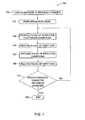
- FIG. 1illustrates an exemplary process sequence 100 for forming an improved tungsten film according to one embodiment of the present invention.
- a substrate to be processedis first loaded into a process chamber capable of performing cyclical deposition and the process conditions are adjusted (step 110 ).
- the substrateis then exposed to one or more borides or derivatives thereof, such as diborane, for about 5 to about 30 seconds (step 120 ).
- a pulse of a tungsten-containing compound accompanied with a suitable carrier gasis introduced into the processing chamber.
- a pulse of inert gasis then pulsed into the processing chamber (step 140 ) to purge or otherwise remove any residual tungsten-containing compound.
- a pulse of a reducing compound accompanied with a suitable carrier gasis introduced into the processing chamber (step 150 ).
- the reducing gasmay be the same compound as the gas used for the boride soak step (step 120 ) or alternatively, the reducing gas may be a different compound, depending on the product throughput requirements and the device applications.
- a pulse of inert gasis then introduced into the processing chamber (step 160 ) to purge or otherwise remove any residual reducing compound.
- Suitable carrier gasesinclude helium (He), argon (Ar), nitrogen (N 2 ), hydrogen (H 2 ), and combinations thereof.
- the borideutilizes argon as a carrier gas and the reducing compound uses hydrogen as the carrier gas.
- Useful purge gasesinclude argon, helium, and combinations thereof.
- a “pulse” as used hereinis intended to refer to a quantity of a particular compound that is intermittently or non-continuously introduced into a reaction zone of a processing chamber.
- the quantity of a particular compound within each pulsemay vary over time, depending on the duration of the pulse.
- the duration of each pulseis variable depending upon a number of factors such as, for example, the volume capacity of the process chamber employed, the vacuum system coupled thereto, and the volatility/reactivity of the particular compound itself.
- each deposition cycleforms a 7 angstrom ( ⁇ ) to 8 ⁇ layer of material.
- subsequent deposition cyclesmay be needed to deposit tungsten nucleation layer having a desired thickness.
- a deposition cycle(steps 130 through 160 ) can be repeated until the desired thickness for the tungsten film is achieved. Thereafter, the process is stopped as indicated by step 180 when the desired thickness is achieved.
- Suitable tungsten-containing compoundsinclude tungsten hexafluoride (WF 6 ) and tungsten carbonyl (W(CO) 6 ), among others, as well as combinations thereof.
- Suitable reducing compoundsinclude, for example, silane (SiH 4 ), disilane (Si 2 H 6 ), dichlorosilane (SiCl 2 H 2 ), borane (BH 3 ), diborane (B 2 H 6 ), triborane (B 3 H 9 ), tetraborane (B 4 H 12 ), pentaborane (B 5 H 15 ), hexaborane (B 6 H 18 ), heptaborane (B 7 H 21 ), octaborane (B 8 H 24 ), nanoborane (B 9 H 27 ), decaborane (B 10 H 30 ), and combinations thereof.
- the cyclical deposition process of FIG. 1typically occurs at a pressure between about 1 Torr and about 90 Torr at a temperature between about 200° C. and about 400° C.
- the boride soak step (step 120 )is typically performed at about 1 Torr and at about 350° C. for about 10 seconds to about 1 minute.
- diboraneis introduced with hydrogen, each having a flowrate between about 300 sccm and about 2,000 sccm.
- the diborane and hydrogen gasesare introduced in a 1:1 volumetric ratio.
- the tungsten-containing compoundis preferably tungsten hexafluoride (WF 6 ) and introduced at a rate of about 5 sccm to about 200 sccm with between about 100 sccm and about 1,000 sccm of argon.
- the reducing compoundis preferably diborane or silane and introduced at a rate between about 5 sccm and about 200 sccm with between about 100 sccm and about 1,000 sccm of hydrogen.
- the pulses of an inert gas, preferably argon, at steps 140 and 160are typically introduced at a rate between about 100 sccm and about 1,000 sccm.
- Each processing step (steps 120 through 160 )lasts about 30 seconds.
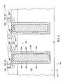
- FIG. 2illustrates a schematic, partial cross section of an exemplary processing chamber 16 useful for depositing a tungsten layer according to the embodiments described above.
- a processing chamber 16is available from Applied Materials, Inc. located in Santa Clara, Calif., and a brief description thereof follows. A more detailed description may be found in commonly assigned U.S. patent application Ser. No. 10/016,300, entitled “Lid Assembly For A Processing System To Facilitate Sequential Deposition Techniques”, filed on Dec. 12, 2001, which is incorporated herein by reference.
- the processing chamber 16includes a chamber body 14 , a lid assembly 20 for gas delivery, and a thermally controlled substrate support member 46 .
- the thermally controlled substrate support member 46includes a wafer support pedestal 48 connected to a support shaft 48 A.
- the thermally controlled substrate support member 46may be moved vertically within the chamber body 14 so that a distance between the support pedestal 48 and the lid assembly 20 may be controlled.
- An example of a lifting mechanism for the support pedestal 48is described in detail in U.S. Pat. No. 5,951,776, issued Sep. 14, 1999to Selyutin et al., entitled “Self-Aligning Lift Mechanism”, which is hereby incorporated by reference in it entirety.
- the support pedestal 48includes an embedded thermocouple 50 A that may be used to monitor the temperature thereof.
- a signal from the thermocouple 50 Amay be used in a feedback loop to control the power applied by a power source 52 to a heater element 52 A.
- the heater element 52 Amay be a resistive heater element or other thermal transfer device disposed within or disposed in contact with the pedestal 48 utilized to control the temperature thereof.
- the support pedestal 48may be heated using a heat transfer fluid (not shown).
- the support pedestal 48may be formed from any process-compatible material, including aluminum nitride and aluminum oxide (Al 2 O 3 or alumina) and may also be configured to hold a substrate 49 thereon employing a vacuum, i.e. support pedestal 48 may be a vacuum chuck. Using a vacuum chuck, the support pedestal 48 may include a plurality of vacuum holes (not shown) that are placed in fluid communication with a vacuum source via the support shaft 48 A.
- the chamber body 14includes a liner assembly 54 having a cylindrical portion and a planar portion.
- the cylindrical portion and the planar portionmay be formed from any suitable material such as aluminum, ceramic and the like.
- the cylindrical portionsurrounds the support pedestal 48 .
- the cylindrical portionalso includes an aperture 60 that aligns with the slit valve opening 44 disposed in a side wall 14 B of the housing 14 to allow entry and egress of substrates from the chamber 16 .
- the planar portion of the liner assembly 54extends transversely to the cylindrical portion and is disposed against a chamber bottom 14 A of the chamber body 14 .
- the liner assembly 54defines a chamber channel 58 between the chamber body 14 and both the cylindrical portion and planar portion of the liner assembly 54 .
- a first portion of channel 58is defined between the chamber bottom 14 A and planar portion of the liner assembly 54 .
- a second portion of channel 58is defined between the sidewall 14 B of the chamber body 14 and the cylindrical portion of the liner assembly 54 .
- a purge gasis introduced into the channel 58 to minimize unwanted deposition on the chamber walls and to control the rate of heat transfer between the chamber walls and the liner assembly 54 .
- the chamber body 14also includes a pumping channel 62 disposed along the sidewalls 14 B thereof.
- the pumping channel 62includes a plurality of apertures, one of which is shown as a first aperture 62 A.
- the pumping channel 62includes a second aperture 62 B that is coupled to a pump system 18 by a conduit 66 .
- a throttle valve 18 Ais coupled between the pumping channel 62 and the pump system 18 .
- the pumping channel 62 , the throttle valve 18 A, and the pump system 18control the amount of gas flow from the processing chamber 16 .
- the size, number, and position of the apertures 62 A in communication with the chamber 16are configured to achieve uniform flow of gases exiting the lid assembly 20 over the support pedestal 48 having a substrate disposed thereon.
- the lid assembly 20includes a lid plate 20 A having a gas manifold 34 mounted thereon.
- the lid plate 20 Aprovides a fluid tight seal with an upper portion of the chamber body 14 when in a closed position.
- the gas manifold 34includes a plurality of control valves 32 (only one shown) to provide rapid and precise gas flow with valve open and close cycles of less than about one second, and in one embodiment, of less than about 0.1 second.
- the valves 32are surface mounted, electronically controlled valves.
- One valve that may be utilizedis available from Fujikin of Japan as part number FR-21-6.35 UGF-APD. Other valves that operate at substantially the same speed and precision may also be used.
- the lid assembly 20further includes a plurality of gas sources 68 A, 68 B, 68 C, each in fluid communication with one of the valves 32 through a sequence of conduits (not shown) formed through the chamber body 14 , lid assembly 20 , and gas manifold 34 .
- the processing chamber 16further includes a reaction zone 75 that is formed within the chamber body 14 when the lid assembly 20 is in a closed position.
- the reaction zone 75includes the volume within the processing chamber 16 that is in fluid communication with a wafer 102 disposed therein.
- the reaction zone 75therefore, includes the volume downstream of each valve 32 within the lid assembly 20 , and the volume between the support pedestal 48 and the lower surface of the lid plate 20 . More particularly, the reaction zone 75 includes the volume between the outlet of each valve 32 and an upper surface of the substrate 49 .
- a controller 70regulates the operations of the various components of the processing chamber 16 .
- the controller 70includes a processor 72 in data communication with memory, such as random access memory 74 and a hard disk drive 76 and is in communication with at least the pump system 18 , the power source 52 , and the valves 32 .
- Software routinesare executed to initiate process recipes or sequences.
- the software routineswhen executed, transform the general purpose computer into a specific process computer that controls the chamber operation so that a chamber process is performed.
- software routinesmay be used to precisely control the activation of the electronic control valves for the execution of process sequences according to the present invention.
- the software routinesmay be performed in hardware, as an application specific integrated circuit or other type of hardware implementation, or a combination of software or hardware.
- a tungsten nucleation layer as described abovehas shown particular utility when integrated with traditional bulk fill techniques to form features with excellent film properties.
- An integration schemecan include cyclical deposition nucleation with bulk fill chemical vapor deposition (CVD) or physical vapor deposition (PVD) processes.
- Integrated processing systems capable of performing such an integration schemeinclude an Endura®, Endura SL®, Centura® and Producer® processing systems, each available from Applied Materials, Inc. located in Santa Clara, Calif. Any of these systems can be configured to include at least one cyclical deposition chamber for depositing the nucleation layer and at least one CVD chamber or PVD chamber for bulk fill.
- FIG. 3is a schematic top-view diagram of an exemplary multi-chamber processing system 300 .
- a similar multi-chamber processing systemis disclosed in U.S. Pat. No. 5,186,718, entitled “Stage Vacuum Wafer Processing System and Method,” issued on Feb. 16, 1993, which is incorporated by reference herein.
- the system 300generally includes load lock chambers 302 , 304 for the transfer of substrates into and out from the system 300 .
- the load lock chambers 302 , 304may “pump down” the substrates introduced into the system 300 .
- a first robot 310may transfer the substrates between the load lock chambers 302 , 304 , and a first set of one or more substrate processing chambers 312 , 314 , 316 , 318 (four are shown). Each processing chamber 312 , 314 , 316 , 318 , can be outfitted to perform a number of substrate processing operations such as cyclical layer deposition, chemical vapor deposition (CVD), physical vapor deposition (PVD), etch, pre-clean, degas, orientation and other substrate processes.
- the first robot 310also transfers substrates to/from one or more transfer chambers 322 , 324 .
- the transfer chambers 322 , 324are used to maintain ultrahigh vacuum conditions while allowing substrates to be transferred within the system 300 .
- a second robot 330may transfer the substrates between the transfer chambers 322 , 324 and a second set of one or more processing chambers 332 , 334 , 336 , 338 .
- the processing chambers 332 , 334 , 336 , 338can be outfitted to perform a variety of substrate processing operations, such as cyclical deposition, chemical vapor deposition (CVD), physical vapor deposition (PVD), etch, pre-clean, degas, and orientation, for example. Any of the substrate processing chambers 312 , 314 , 316 , 318 , 332 , 334 , 336 , 338 may be removed from the system 300 if not necessary for a particular process to be performed by the system 300 .
- each processing chamber 332 and 338may be a cyclical deposition chamber adapted to deposit a nucleation layer; each processing chamber 334 and 336 may be a cyclical deposition chamber, a chemical vapor deposition chamber, or a physical vapor deposition chamber adapted to form a bulk fill deposition layer; each processing chamber 312 and 314 may be a physical vapor deposition chamber, a chemical vapor deposition chamber, or a cyclical deposition chamber adapted to deposit a dielectric layer; and each processing chamber 316 and 318 may be an etch chamber outfitted to etch apertures or openings for interconnect features.
- This one particular arrangement of the system 300is provided to illustrate the invention and should not be used to limit the scope of the invention.
- Another integrated systemmay include nucleation deposition as well as bulk fill deposition in a single chamber.
- a chamberconfigured to operate in both a cyclical deposition mode as well as a conventional CVD mode can be used.
- One example of such a chamberis described in U.S. patent application Ser. No. 10/016,300, filed on Dec. 12, 2001, which is incorporated herein by reference.
- one or more cyclical deposition nucleation chambersare integrated onto a first processing system while one or more bulk layer deposition chambers are integrated onto a second processing system.
- substratesare first processed in the first system where a nucleation layer is deposited on a substrate. Thereafter, the substrates are moved to the second processing system where bulk deposition occurs.
- a carousel type batch processing system having a plurality of stations in a single chambercan be adapted to incorporate nucleation and bulk layer deposition into a single processing system.
- a purge gas curtainsuch as an argon gas curtain
- the substratesare loaded into the system sequentially and then rotated through each station and processed at least partially at each station.
- a substratemay be exposed to a cyclical deposition nucleation step at a first station and then to partial bulk fill CVD steps at each of the subsequent stations.
- nucleationmay occur at more than one station and bulk fill may occur at one or more stations.
- the nucleation layer and the bulk layermay be deposited in separate carousel type systems.
- Each platencan be temperature controlled to provide at least some process control at each station.
- the process pressuretypically remains the same between stations because the stations are housed in a single chamber.
- Some pressure controlmay be available in a micro or mini environment present at each station due to the inert gas curtain.
- the nucleation layeris typically deposited to a thickness ranging from about 10 angstroms to about 200 angstroms and the bulk fill has a thickness between about 1,000 angstroms and about 10,000 angstroms.
- the thickness of these filmscan vary depending on the feature sizes and aspect ratios of a given application. Accordingly, the films are suitably sized to accommodate the geometries of a given application.
- the followingare some exemplary geometries and applications that can benefit from a nucleation layer deposited according to embodiments described herein. The following descriptions are intended for illustrative purposes only, and are not intended to limit the uses of the present invention.
- FIG. 4shows a cross sectional view of an exemplary metal oxide gate device 400 utilizing a nucleation layer deposited according to embodiments described herein.
- the device 400generally includes an exposed gate 410 surrounded by spacers 416 and silicon source/drain areas 420 formed within a substrate surface 412 .
- the spacers 416typically include an oxide, such as silicon dioxide, or a nitride, such as silicon nitride.
- the metal gate 410includes an oxide layer 411 , a polysilicon layer 414 , a titanium nitride barrier layer 415 , and a tungsten layer 422 .
- the oxide layer 411separates the substrate 412 from the polysilicon layer 414 .
- the oxide layer 411 and the polysilicon layer 414are deposited using conventional deposition techniques.
- the titanium nitride barrier layer 415is deposited on the polysilicon layer 414 .
- the titanium nitride barrier layer 415may be a bi-layer stack formed by depositing a PVD titanium layer followed by a CVD titanium nitride layer.
- the titanium barrier layer 415may also be deposited using a cyclical deposition technique, such as the process shown and described in co-pending U.S. patent application Ser. No. 10/032,293, filed on Dec. 21, 2001, entitled “Chamber Hardware Design for Titanium Nitride Atomic Layer Deposition”, which is incorporated by reference herein.
- a nucleation layer 417is then cyclically deposited over the barrier layer 415 following treatment of the substrate surface with the diborane soak process described above.
- the nucleation layer 417is cyclically deposited using alternating pulses of tungsten hexafluoride (WF 6 ) and diborane (B 2 H 6 ).
- the tungsten hexafluoride (WF 6 )is pulsed at a rate of between about 10 sccm and about 400 sccm, such as between about 20 sccm and about 100 sccm, for about 30 seconds.
- a carrier gassuch as argon, is provided along with the tungsten hexafluoride at a rate of about 250 sccm to about 1000 sccm, such as between about 500 sccm to about 750 sccm.
- the diborane (B 2 H 6 )is pulsed at a rate of about 5 sccm and about 150 sccm, such as between about 5 sccm and about 25 sccm, for about 30 seconds.
- a carrier gas, such as hydrogenis provided along with the diborane at a rate between about 250 sccm to about 1000 sccm, such as between about 500 sccm to about 750 sccm.
- the substrateis maintained at a temperature between about 250° C. and about 350° C. at a chamber pressure between about 1 torr and about 10 torr.
- argonis pulsed for about 30 seconds to purge or otherwise remove any reactive compounds from the processing chamber.
- the nucleation layer 417is cyclically deposited using alternating pulses of tungsten hexafluoride (WF 6 ) and silane (SiH 4 ).
- the tungsten hexafluoride (WF 6 )is pulsed as described above with argon for about 30 seconds.
- the silane (SiH 4 )is pulsed at a rate of about 10 sccm to about 500 sccm, such as between about 50 sccm to about 200 sccm, for about 30 seconds.
- a carrier gassuch as hydrogen
- Argonis pulsed at a rate of about 300 sccm to about 1000 sccm, such as between about 500 sccm to about 750 sccm, for about 30 seconds between the pulses of the tungsten hexafluoride (WF 6 ) and the pulses of silane (SiH 4 ).
- the substrateis maintained at a temperature between about 300° C. and about 400° C. at a chamber pressure between about 1 torr and about 10 torr.
- a nucleation layer formed by alternating pulses of tungsten hexafluoride (WF 6 ) and diborane without a boride soak treatmenthas advantages over a nucleation layer formed by alternating pulses of tungsten hexafluoride (WF 6 ) and silane.
- the diborane filmshows lower stress for the integrated film and reduced fluorine content at the interface of the nucleation layer.
- the amorphous nature of the diborane filmalso permits thinner nucleation layers to be used, while maintaining good barrier properties.
- a nucleation layer formed by alternating pulses of tungsten hexafluoride (WF 6 ) and silane after a boride soak treatmenteliminates the advantages the diborane deposition has over the silane deposition. Therefore, the nucleation layer 417 is preferably formed using alternating pulses of tungsten hexafluoride (WF 6 ) and silane following the diborane soak.
- a tungsten bulk fill 422is then deposited on the tungsten nucleation layer 417 .
- the tungsten bulk fill 422may be deposited by alternately adsorbing a tungsten-containing compound and a reducing gas as described above.
- a more detailed description of tungsten deposition using a cyclical deposition techniquemay be found in commonly assigned U.S. patent application Ser. No. 10/016,300, entitled “Lid Assembly For A Processing System To Facilitate Sequential Deposition Techniques”, filed on Dec. 12, 2001; and in commonly assigned U.S. Patent Application No. (unknown), entitled “Deposition Of Tungsten Films For Dynamic Random Access Memory (DRAM) Application”, filed on Feb. 20, 2002, which are both incorporated herein by reference.
- the top portion of the resulting structure 400may be planarized.
- a chemical mechanical polishing (CMP) apparatusmay be used, such as the MirraTM System available from Applied Materials, Santa Clara, Calif., for example.
- CMPchemical mechanical polishing
- portions of the tungsten bulk fill 422are removed from the top of the structure leaving a fully planar surface.
- the intermediate surfaces of the structuremay be planarized between the deposition of the subsequent layers described above.
- FIG. 5is a cross sectional view of a conventional DRAM device having a transistor 520 positioned adjacent a top portion of a trench capacitor 530 .
- the access transistor 520 for the DRAM device 510is positioned adjacent a top portion of the trench capacitor 530 .
- the access transistor 520comprises an n-p-n transistor having a source region 522 , a gate region 524 , and a drain region 526 .
- the gate region 524is a P-doped silicon epi-layer disposed over the P+ substrate.
- the source region 522 of the access transistor 520is an N+ doped material disposed on a first side of the gate region 524
- the drain region 526is an N+ doped material disposed on a second side of the gate region 524 , opposite the source region 522 .
- the source and drain regions 522 , 524may be connected to a tungsten plug 560 .
- Each tungsten plug 560includes a titanium liner 562 , a tungsten nucleation layer 564 , and a bulk tungsten fill 566 .
- the titanium liner 562may be a bi-layer stack comprising PVD titanium followed by CVD titanium nitride.
- the tungsten nucleation layer 564is formed using the cyclical deposition technique as described above.
- the tungsten bulk fill 566may be deposited using any conventional deposition technique.
- the trench capacitor 530generally includes a first electrode 532 , a second electrode 534 and a dielectric material 536 disposed therebetween.
- the P+ substrateserves as a first electrode 532 of the trench capacitor 530 and is connected to a ground connection 541 .
- a trench 538is formed in the P+ substrate and filled with a heavily doped N+ polysilicon that serves as the second electrode 534 of the trench capacitor 530 .
- the dielectric material 536is disposed between the first electrode 532 (i.e., P+ substrate) and the second electrode 534 (i.e., N+ polysilicon).
- the trench capacitor 530also includes a first tungsten nitride barrier layer 540 disposed between the dielectric material 536 and the first electrode 532 .
- a second tungsten nitride barrier layer 542is disposed between the dielectric material 536 and the second electrode 534 .
- the barrier layers 540 , 542are a combination film, such as W/WN.
- DRAM deviceutilizes an n-p-n transistor, a P+ substrate as a first electrode, and an N+ polysilicon as a second electrode of the capacitor
- transistor designs and electrode materialsare contemplated by the present invention to form DRAM devices.
- other devices, such as crown capacitors for example,are contemplated by the present invention.
- Tititanium
- TiNtitanium nitride
- ALDatomic layer deposition
- Durationabout 10 seconds.
- tungsten nucleation layerwas formed on the barrier layer using the cyclical deposition techniques described herein.
- the nucleation layerhad a thickness of about 100 ⁇ .
- a bulk tungsten layerwas deposited on the nucleation layer using CVD to a thickness of about 2,500 ⁇ .
- the resulting tungsten bulk fill filmexhibited a uniformity variance of less than about 2 percent.
- Tititanium
- TiNtitanium nitride
- ALDatomic layer deposition
- Durationabout 60 seconds.
- tungsten nucleation layerwas formed on the barrier layer using the cyclical deposition techniques described herein.
- the nucleation layerhad a thickness of about 100 ⁇ .
- a bulk tungsten layerwas deposited on the nucleation layer using CVD to a thickness of about 2,500 ⁇ .
- the resulting tungsten bulk fill filmexhibited an uniformity variance greater than about 5 percent.
- the tungsten film deposited using a boride soak processexhibited an improved surface uniformity compared to a tungsten film deposited using a silane soak process.
- the boride soak processis at least six times faster than the silane soak, which does not take into account the down time to pressurize the processing chamber to 90 Torr required by the silane soak treatment. Accordingly, the boride soak treatment of the present invention exhibits improved film uniformity and a significant increase in product throughput.
Landscapes
- Chemical & Material Sciences (AREA)
- General Chemical & Material Sciences (AREA)
- Chemical Kinetics & Catalysis (AREA)
- Engineering & Computer Science (AREA)
- Materials Engineering (AREA)
- Mechanical Engineering (AREA)
- Metallurgy (AREA)
- Organic Chemistry (AREA)
- Chemical Vapour Deposition (AREA)
- Electrodes Of Semiconductors (AREA)
- Semiconductor Memories (AREA)
- Insulated Gate Type Field-Effect Transistor (AREA)
- Internal Circuitry In Semiconductor Integrated Circuit Devices (AREA)
Abstract
Description
This application is related to co-pending U.S. patent application Ser. No. 60/328,451, entitled “Method and Apparatus for Depositing Refractory Metal Layers Employing Sequential Deposition Techniques”, filed on Oct. 10, 2001, which is incorporated by reference herein.
1. Field of the Invention
Embodiments of the invention relate to the processing of semiconductor substrates. More particularly, embodiments of the invention relate to deposition of refractory metal layers on semiconductor substrates.
2. Description of the Related Art
The semiconductor processing industry continues to strive for larger production yields while increasing the uniformity of layers deposited on substrates having larger surface areas. These same factors in combination with new materials also provide higher integration of circuits per unit area of the substrate. As circuit integration increases, the need for greater uniformity and process control regarding layer thickness rises. As a result, various technologies have been developed to deposit layers on substrates in a cost-effective manner, while maintaining control over the characteristics of the layer.
Chemical Vapor Deposition (CVD) is one of the most common deposition processes employed for depositing layers on a substrate. CVD is a flux-dependent deposition technique that requires precise control of the substrate temperature and the precursors introduced into the processing chamber in order to produce a desired layer of uniform thickness. These requirements become more critical as substrate size increases, creating a need for more complexity in chamber design and gas flow technique to maintain adequate uniformity.
A variant of CVD that demonstrates superior step coverage, compared to CVD, is cyclical Deposition. Cyclical deposition is based upon Atomic Layer Epitaxy (ALE) and employs chemisorption to deposit a saturated monolayer of reactive precursor molecules on a substrate surface. This is achieved by alternatingly pulsing an appropriate reactive precursor into a deposition chamber. Each injection of a reactive precursor is separated by an inert gas purge to provide a new atomic layer additive to previously deposited layers to form a uniform layer on the substrate. The cycle is repeated to form the layer to a desired thickness.
Formation of film layers at a high deposition rate while providing adequate step coverage are conflicting characteristics often necessitating the sacrifice of one to obtain the other. This conflict is true particularly when refractory metal layers are deposited to cover gaps or vias during the formation of contacts interconnecting adjacent metallic layers separated by dielectric layers. Historically, CVD techniques have been employed to deposit conductive material such as refractory metals in order to inexpensively and quickly form contacts. Due to the increasing integration of semiconductor circuitry, tungsten has been used based upon superior step coverage. As a result, deposition of tungsten employing CVD techniques enjoys wide application in semiconductor processing due to the high throughput of the process.
Depositing tungsten by traditional CVD methods, however, is attendant with several disadvantages. For example, blanket deposition of a tungsten layer on a semiconductor wafer is time-consuming at temperatures below 400° C. The deposition rate of tungsten may be improved by increasing the deposition temperature to, for example, about 500° C. to about 550° C. However, temperatures in this higher range may compromise the structural and operational integrity of the underlying portions of the integrated circuit being formed. Use of tungsten has also frustrated photolithography steps during the manufacturing process as it results in a relatively rough surface having a reflectivity of 20% or less than that of a silicon substrate. Further, tungsten has proven difficult to deposit uniformly. Poor surface uniformity typically increases film resistivity.
Therefore, there is a need for an improved technique to deposit conductive layers with good uniformity using cyclical deposition techniques.
Embodiments of the invention include an improved method for forming a tungsten layer on a substrate surface. In one aspect, the method includes positioning the substrate surface in a processing chamber, exposing the substrate surface to a boride, and depositing a nucleation layer in the same processing chamber by alternately pulsing a tungsten-containing compound and a reducing gas selected from a group consisting of silane (SiH4), disilane (Si2H6), dichlorosilane (SiCl2H2), derivatives thereof, and combinations thereof.
In another aspect, the method includes exposing the substrate surface to a boride, depositing a nucleation layer in the same processing chamber by alternately pulsing a tungsten-containing compound and silane gas, and forming a bulk tungsten deposition film on the nucleation layer.
In yet another aspect, the method includes exposing the substrate surface to diborane, depositing a nucleation layer by alternately pulsing a tungsten-containing compound and silane gas, and forming a bulk tungsten deposition film on the nucleation layer. The bulk tungsten deposition film may be deposited using cyclical deposition, chemical vapor deposition, or physical vapor deposition techniques.
So that the manner in which the above recited features of the present invention can be understood in detail, a more particular description of the invention, briefly summarized above, may be had by reference to embodiments, some of which are illustrated in the appended drawings. It is to be noted, however, that the appended drawings illustrate only typical embodiments of this invention and are therefore not to be considered limiting of its scope, for the invention may admit to other equally effective embodiments.
FIG. 1 illustrates a process sequence for the formation of a tungsten layer using a cyclical deposition technique according to one embodiment described herein.
FIG. 2 depicts a schematic cross-sectional view of a process chamber useful for practicing the cyclical deposition techniques described herein.
FIG. 3 shows an exemplary integrated processing platform.
FIG. 4 shows a cross sectional view of an exemplary metal oxide gate device formed according to embodiments of the present invention.
FIG. 5 shows a cross sectional view of a conventional DRAM device formed according to embodiments of the present invention.
Embodiments of the invention provide an improved process for depositing tungsten films. The process utilizes a cyclical deposition technique and provides tungsten films having significantly improved surface uniformity and significantly increased production throughput. In one aspect, the process includes a boride soak prior to tungsten deposition to activate the underlying substrate surface. Preferably, the underlying surface is exposed to diborane (B2H6) although it is believed that any boride and derivatives thereof achieve similar results. In general, the boride soak occurs in-situ for about 5 to about 30 seconds at similar processing conditions as a subsequent tungsten cyclical deposition process, thereby significantly increasing production throughput.
A “substrate surface”, as used herein, refers to any substrate surface upon which film processing is performed. For example, a substrate surface may include silicon, silicon oxide, doped silicon, germanium, gallium arsenide, glass, sapphire, and any other materials such as metals, metal nitrides, metal alloys, and other conductive materials, depending on the application. A substrate surface may also include dielectric materials such as silicon dioxide and carbon doped silicon oxides.
“Cyclical deposition” as used herein refers to the sequential introduction of two or more reactive compounds to deposit a mono layer of material on a substrate surface. The two or more reactive compounds are alternatively introduced into a reaction zone of a processing chamber. Each reactive compound is separated by a time delay to allow each compound to adhere and/or react on the substrate surface. In one aspect, a first precursor or compound A is pulsed into the reaction zone followed by a first time delay. Next, a second precursor or compound B is pulsed into the reaction zone followed by a second delay. During each time delay an inert gas, such as argon, is introduced into the processing chamber to purge the reaction zone or otherwise remove any residual reactive compound from the reaction zone. Alternatively, the purge gas may flow continuously throughout the deposition process so that only the purge gas flows during the time delay between pulses of reactive compounds. The reactive compounds are alternatively pulsed until a desired film or film thickness is formed on the substrate surface.
FIG. 1 illustrates anexemplary process sequence 100 for forming an improved tungsten film according to one embodiment of the present invention. A substrate to be processed is first loaded into a process chamber capable of performing cyclical deposition and the process conditions are adjusted (step110). The substrate is then exposed to one or more borides or derivatives thereof, such as diborane, for about 5 to about 30 seconds (step120). Atstep 130, a pulse of a tungsten-containing compound accompanied with a suitable carrier gas is introduced into the processing chamber. A pulse of inert gas is then pulsed into the processing chamber (step140) to purge or otherwise remove any residual tungsten-containing compound. Next, a pulse of a reducing compound accompanied with a suitable carrier gas is introduced into the processing chamber (step150). The reducing gas may be the same compound as the gas used for the boride soak step (step120) or alternatively, the reducing gas may be a different compound, depending on the product throughput requirements and the device applications. A pulse of inert gas is then introduced into the processing chamber (step160) to purge or otherwise remove any residual reducing compound.
Suitable carrier gases include helium (He), argon (Ar), nitrogen (N2), hydrogen (H2), and combinations thereof. Typically, the boride utilizes argon as a carrier gas and the reducing compound uses hydrogen as the carrier gas. Useful purge gases include argon, helium, and combinations thereof.
A “pulse” as used herein is intended to refer to a quantity of a particular compound that is intermittently or non-continuously introduced into a reaction zone of a processing chamber. The quantity of a particular compound within each pulse may vary over time, depending on the duration of the pulse. The duration of each pulse is variable depending upon a number of factors such as, for example, the volume capacity of the process chamber employed, the vacuum system coupled thereto, and the volatility/reactivity of the particular compound itself.
Referring to step170, after each deposition cycle (steps 130 through160), a tungsten nucleation layer having a particular thickness will be deposited on the substrate surface. Usually, each deposition cycle forms a 7 angstrom (Å) to 8 Å layer of material. Depending on specific device requirements, subsequent deposition cycles may be needed to deposit tungsten nucleation layer having a desired thickness. As such, a deposition cycle (steps 130 through160) can be repeated until the desired thickness for the tungsten film is achieved. Thereafter, the process is stopped as indicated bystep 180 when the desired thickness is achieved.
Suitable tungsten-containing compounds include tungsten hexafluoride (WF6) and tungsten carbonyl (W(CO)6), among others, as well as combinations thereof. Suitable reducing compounds include, for example, silane (SiH4), disilane (Si2H6), dichlorosilane (SiCl2H2), borane (BH3), diborane (B2H6), triborane (B3H9), tetraborane (B4H12), pentaborane (B5H15), hexaborane (B6H18), heptaborane (B7H21), octaborane (B8H24), nanoborane (B9H27), decaborane (B10H30), and combinations thereof.
The cyclical deposition process of FIG. 1 typically occurs at a pressure between about 1 Torr and about 90 Torr at a temperature between about 200° C. and about 400° C. The boride soak step (step120) is typically performed at about 1 Torr and at about 350° C. for about 10 seconds to about 1 minute. In one aspect, diborane is introduced with hydrogen, each having a flowrate between about 300 sccm and about 2,000 sccm. Preferably, the diborane and hydrogen gases are introduced in a 1:1 volumetric ratio. Instep 130, the tungsten-containing compound is preferably tungsten hexafluoride (WF6) and introduced at a rate of about 5 sccm to about 200 sccm with between about 100 sccm and about 1,000 sccm of argon. Instep 150, the reducing compound is preferably diborane or silane and introduced at a rate between about 5 sccm and about 200 sccm with between about 100 sccm and about 1,000 sccm of hydrogen. The pulses of an inert gas, preferably argon, atsteps steps 120 through160) lasts about 30 seconds.
FIG. 2 illustrates a schematic, partial cross section of anexemplary processing chamber 16 useful for depositing a tungsten layer according to the embodiments described above. Such aprocessing chamber 16 is available from Applied Materials, Inc. located in Santa Clara, Calif., and a brief description thereof follows. A more detailed description may be found in commonly assigned U.S. patent application Ser. No. 10/016,300, entitled “Lid Assembly For A Processing System To Facilitate Sequential Deposition Techniques”, filed on Dec. 12, 2001, which is incorporated herein by reference.
Referring to FIG. 2, theprocessing chamber 16 includes achamber body 14, alid assembly 20 for gas delivery, and a thermally controlledsubstrate support member 46. The thermally controlledsubstrate support member 46 includes awafer support pedestal 48 connected to asupport shaft 48A. The thermally controlledsubstrate support member 46 may be moved vertically within thechamber body 14 so that a distance between thesupport pedestal 48 and thelid assembly 20 may be controlled. An example of a lifting mechanism for thesupport pedestal 48 is described in detail in U.S. Pat. No. 5,951,776, issued Sep. 14, 1999to Selyutin et al., entitled “Self-Aligning Lift Mechanism”, which is hereby incorporated by reference in it entirety.
Thesupport pedestal 48 includes an embeddedthermocouple 50A that may be used to monitor the temperature thereof. For example, a signal from thethermocouple 50A may be used in a feedback loop to control the power applied by apower source 52 to aheater element 52A. Theheater element 52A may be a resistive heater element or other thermal transfer device disposed within or disposed in contact with thepedestal 48 utilized to control the temperature thereof. Optionally, thesupport pedestal 48 may be heated using a heat transfer fluid (not shown).
Thesupport pedestal 48 may be formed from any process-compatible material, including aluminum nitride and aluminum oxide (Al2O3or alumina) and may also be configured to hold asubstrate 49 thereon employing a vacuum, i.e.support pedestal 48 may be a vacuum chuck. Using a vacuum chuck, thesupport pedestal 48 may include a plurality of vacuum holes (not shown) that are placed in fluid communication with a vacuum source via thesupport shaft 48A.
Thechamber body 14 includes aliner assembly 54 having a cylindrical portion and a planar portion. The cylindrical portion and the planar portion may be formed from any suitable material such as aluminum, ceramic and the like. The cylindrical portion surrounds thesupport pedestal 48. The cylindrical portion also includes anaperture 60 that aligns with the slit valve opening44 disposed in aside wall 14B of thehousing 14 to allow entry and egress of substrates from thechamber 16.
The planar portion of theliner assembly 54 extends transversely to the cylindrical portion and is disposed against achamber bottom 14A of thechamber body 14. Theliner assembly 54 defines achamber channel 58 between thechamber body 14 and both the cylindrical portion and planar portion of theliner assembly 54. Specifically, a first portion ofchannel 58 is defined between thechamber bottom 14A and planar portion of theliner assembly 54. A second portion ofchannel 58 is defined between thesidewall 14B of thechamber body 14 and the cylindrical portion of theliner assembly 54. A purge gas is introduced into thechannel 58 to minimize unwanted deposition on the chamber walls and to control the rate of heat transfer between the chamber walls and theliner assembly 54.
Thechamber body 14 also includes a pumpingchannel 62 disposed along the sidewalls14B thereof. The pumpingchannel 62 includes a plurality of apertures, one of which is shown as afirst aperture 62A. The pumpingchannel 62 includes asecond aperture 62B that is coupled to apump system 18 by aconduit 66. Athrottle valve 18A is coupled between the pumpingchannel 62 and thepump system 18. The pumpingchannel 62, thethrottle valve 18A, and thepump system 18 control the amount of gas flow from theprocessing chamber 16. The size, number, and position of theapertures 62A in communication with thechamber 16 are configured to achieve uniform flow of gases exiting thelid assembly 20 over thesupport pedestal 48 having a substrate disposed thereon.
Thelid assembly 20 includes a lid plate20A having agas manifold 34 mounted thereon. The lid plate20A provides a fluid tight seal with an upper portion of thechamber body 14 when in a closed position. Thegas manifold 34 includes a plurality of control valves32 (only one shown) to provide rapid and precise gas flow with valve open and close cycles of less than about one second, and in one embodiment, of less than about 0.1 second. Thevalves 32 are surface mounted, electronically controlled valves. One valve that may be utilized is available from Fujikin of Japan as part number FR-21-6.35 UGF-APD. Other valves that operate at substantially the same speed and precision may also be used.
Thelid assembly 20 further includes a plurality ofgas sources valves 32 through a sequence of conduits (not shown) formed through thechamber body 14,lid assembly 20, andgas manifold 34.
Theprocessing chamber 16 further includes areaction zone 75 that is formed within thechamber body 14 when thelid assembly 20 is in a closed position. Generally, thereaction zone 75 includes the volume within theprocessing chamber 16 that is in fluid communication with a wafer102 disposed therein. Thereaction zone 75, therefore, includes the volume downstream of eachvalve 32 within thelid assembly 20, and the volume between thesupport pedestal 48 and the lower surface of thelid plate 20. More particularly, thereaction zone 75 includes the volume between the outlet of eachvalve 32 and an upper surface of thesubstrate 49.
Acontroller 70 regulates the operations of the various components of theprocessing chamber 16. Thecontroller 70 includes aprocessor 72 in data communication with memory, such asrandom access memory 74 and ahard disk drive 76 and is in communication with at least thepump system 18, thepower source 52, and thevalves 32.
Software routines are executed to initiate process recipes or sequences. The software routines, when executed, transform the general purpose computer into a specific process computer that controls the chamber operation so that a chamber process is performed. For example, software routines may be used to precisely control the activation of the electronic control valves for the execution of process sequences according to the present invention. Alternatively, the software routines may be performed in hardware, as an application specific integrated circuit or other type of hardware implementation, or a combination of software or hardware.
Process Integration
A tungsten nucleation layer as described above has shown particular utility when integrated with traditional bulk fill techniques to form features with excellent film properties. An integration scheme can include cyclical deposition nucleation with bulk fill chemical vapor deposition (CVD) or physical vapor deposition (PVD) processes. Integrated processing systems capable of performing such an integration scheme include an Endura®, Endura SL®, Centura® and Producer® processing systems, each available from Applied Materials, Inc. located in Santa Clara, Calif. Any of these systems can be configured to include at least one cyclical deposition chamber for depositing the nucleation layer and at least one CVD chamber or PVD chamber for bulk fill.
FIG. 3 is a schematic top-view diagram of an exemplary multi-chamber processing system300. A similar multi-chamber processing system is disclosed in U.S. Pat. No. 5,186,718, entitled “Stage Vacuum Wafer Processing System and Method,” issued on Feb. 16, 1993, which is incorporated by reference herein. The system300 generally includesload lock chambers load lock chambers first robot 310 may transfer the substrates between theload lock chambers substrate processing chambers processing chamber first robot 310 also transfers substrates to/from one ormore transfer chambers
Thetransfer chambers second robot 330 may transfer the substrates between thetransfer chambers more processing chambers chambers processing chambers substrate processing chambers
In one arrangement, eachprocessing chamber processing chamber processing chamber processing chamber
Another integrated system may include nucleation deposition as well as bulk fill deposition in a single chamber. A chamber configured to operate in both a cyclical deposition mode as well as a conventional CVD mode can be used. One example of such a chamber is described in U.S. patent application Ser. No. 10/016,300, filed on Dec. 12, 2001, which is incorporated herein by reference.
In another integration scheme, one or more cyclical deposition nucleation chambers are integrated onto a first processing system while one or more bulk layer deposition chambers are integrated onto a second processing system. In this configuration, substrates are first processed in the first system where a nucleation layer is deposited on a substrate. Thereafter, the substrates are moved to the second processing system where bulk deposition occurs.
Alternatively, a carousel type batch processing system having a plurality of stations in a single chamber can be adapted to incorporate nucleation and bulk layer deposition into a single processing system. In such a processing system a purge gas curtain, such as an argon gas curtain, can be established between each station creating a micro or mini environment at each station. The substrates are loaded into the system sequentially and then rotated through each station and processed at least partially at each station. For example, a substrate may be exposed to a cyclical deposition nucleation step at a first station and then to partial bulk fill CVD steps at each of the subsequent stations. Alternatively, nucleation may occur at more than one station and bulk fill may occur at one or more stations. Still further, the nucleation layer and the bulk layer may be deposited in separate carousel type systems. Each platen can be temperature controlled to provide at least some process control at each station. However, the process pressure typically remains the same between stations because the stations are housed in a single chamber. Some pressure control may be available in a micro or mini environment present at each station due to the inert gas curtain.
Regardless of the integration scheme, the nucleation layer is typically deposited to a thickness ranging from about 10 angstroms to about 200 angstroms and the bulk fill has a thickness between about 1,000 angstroms and about 10,000 angstroms. However, the thickness of these films can vary depending on the feature sizes and aspect ratios of a given application. Accordingly, the films are suitably sized to accommodate the geometries of a given application. The following are some exemplary geometries and applications that can benefit from a nucleation layer deposited according to embodiments described herein. The following descriptions are intended for illustrative purposes only, and are not intended to limit the uses of the present invention.
Tungsten Metal Gate
FIG. 4 shows a cross sectional view of an exemplary metaloxide gate device 400 utilizing a nucleation layer deposited according to embodiments described herein. Thedevice 400 generally includes an exposedgate 410 surrounded byspacers 416 and silicon source/drain areas 420 formed within asubstrate surface 412. Thespacers 416 typically include an oxide, such as silicon dioxide, or a nitride, such as silicon nitride.
Themetal gate 410 includes anoxide layer 411, apolysilicon layer 414, a titaniumnitride barrier layer 415, and atungsten layer 422. Theoxide layer 411 separates thesubstrate 412 from thepolysilicon layer 414. Theoxide layer 411 and thepolysilicon layer 414 are deposited using conventional deposition techniques.
The titaniumnitride barrier layer 415 is deposited on thepolysilicon layer 414. The titaniumnitride barrier layer 415 may be a bi-layer stack formed by depositing a PVD titanium layer followed by a CVD titanium nitride layer. Thetitanium barrier layer 415 may also be deposited using a cyclical deposition technique, such as the process shown and described in co-pending U.S. patent application Ser. No. 10/032,293, filed on Dec. 21, 2001, entitled “Chamber Hardware Design for Titanium Nitride Atomic Layer Deposition”, which is incorporated by reference herein.
Anucleation layer 417 is then cyclically deposited over thebarrier layer 415 following treatment of the substrate surface with the diborane soak process described above. In one aspect, thenucleation layer 417 is cyclically deposited using alternating pulses of tungsten hexafluoride (WF6) and diborane (B2H6). The tungsten hexafluoride (WF6) is pulsed at a rate of between about 10 sccm and about 400 sccm, such as between about 20 sccm and about 100 sccm, for about 30 seconds. A carrier gas, such as argon, is provided along with the tungsten hexafluoride at a rate of about 250 sccm to about 1000 sccm, such as between about 500 sccm to about 750 sccm. The diborane (B2H6) is pulsed at a rate of about 5 sccm and about 150 sccm, such as between about 5 sccm and about 25 sccm, for about 30 seconds. A carrier gas, such as hydrogen, is provided along with the diborane at a rate between about 250 sccm to about 1000 sccm, such as between about 500 sccm to about 750 sccm. The substrate is maintained at a temperature between about 250° C. and about 350° C. at a chamber pressure between about 1 torr and about 10 torr. In between pulses of the tungsten hexafluoride and the diborane, argon is pulsed for about 30 seconds to purge or otherwise remove any reactive compounds from the processing chamber.
In another aspect, thenucleation layer 417 is cyclically deposited using alternating pulses of tungsten hexafluoride (WF6) and silane (SiH4). The tungsten hexafluoride (WF6) is pulsed as described above with argon for about 30 seconds. The silane (SiH4) is pulsed at a rate of about 10 sccm to about 500 sccm, such as between about 50 sccm to about 200 sccm, for about 30 seconds. A carrier gas, such as hydrogen, is provided along with the silane at a rate of about 250 sccm and about 1000 sccm, such as between about 300 sccm and about 500 sccm. Argon is pulsed at a rate of about 300 sccm to about 1000 sccm, such as between about 500 sccm to about 750 sccm, for about 30 seconds between the pulses of the tungsten hexafluoride (WF6) and the pulses of silane (SiH4). The substrate is maintained at a temperature between about 300° C. and about 400° C. at a chamber pressure between about 1 torr and about 10 torr.
A nucleation layer formed by alternating pulses of tungsten hexafluoride (WF6) and diborane without a boride soak treatment has advantages over a nucleation layer formed by alternating pulses of tungsten hexafluoride (WF6) and silane. The diborane film shows lower stress for the integrated film and reduced fluorine content at the interface of the nucleation layer. The amorphous nature of the diborane film also permits thinner nucleation layers to be used, while maintaining good barrier properties. However, a nucleation layer formed by alternating pulses of tungsten hexafluoride (WF6) and silane after a boride soak treatment, as described herein, eliminates the advantages the diborane deposition has over the silane deposition. Therefore, thenucleation layer 417 is preferably formed using alternating pulses of tungsten hexafluoride (WF6) and silane following the diborane soak.
A tungsten bulk fill422 is then deposited on thetungsten nucleation layer 417. Although any metal deposition process, such as conventional chemical vapor deposition or physical vapor deposition, may be used, the tungsten bulk fill422 may be deposited by alternately adsorbing a tungsten-containing compound and a reducing gas as described above. A more detailed description of tungsten deposition using a cyclical deposition technique may be found in commonly assigned U.S. patent application Ser. No. 10/016,300, entitled “Lid Assembly For A Processing System To Facilitate Sequential Deposition Techniques”, filed on Dec. 12, 2001; and in commonly assigned U.S. Patent Application No. (unknown), entitled “Deposition Of Tungsten Films For Dynamic Random Access Memory (DRAM) Application”, filed on Feb. 20, 2002, which are both incorporated herein by reference.
Following deposition, the top portion of the resultingstructure 400 may be planarized. A chemical mechanical polishing (CMP) apparatus may be used, such as the Mirra™ System available from Applied Materials, Santa Clara, Calif., for example. For example, portions of the tungsten bulk fill422 are removed from the top of the structure leaving a fully planar surface. Optionally, the intermediate surfaces of the structure may be planarized between the deposition of the subsequent layers described above.
Logic Device
FIG. 5 is a cross sectional view of a conventional DRAM device having atransistor 520 positioned adjacent a top portion of atrench capacitor 530. Theaccess transistor 520 for theDRAM device 510 is positioned adjacent a top portion of thetrench capacitor 530. Preferably, theaccess transistor 520 comprises an n-p-n transistor having asource region 522, agate region 524, and adrain region 526. Thegate region 524 is a P-doped silicon epi-layer disposed over the P+ substrate. Thesource region 522 of theaccess transistor 520 is an N+ doped material disposed on a first side of thegate region 524, and thedrain region 526 is an N+ doped material disposed on a second side of thegate region 524, opposite thesource region 522.
The source and drainregions tungsten plug 560. Eachtungsten plug 560 includes atitanium liner 562, atungsten nucleation layer 564, and abulk tungsten fill 566. Thetitanium liner 562 may be a bi-layer stack comprising PVD titanium followed by CVD titanium nitride. Thetungsten nucleation layer 564 is formed using the cyclical deposition technique as described above. The tungsten bulk fill566 may be deposited using any conventional deposition technique.
Thetrench capacitor 530 generally includes afirst electrode 532, asecond electrode 534 and adielectric material 536 disposed therebetween. The P+ substrate serves as afirst electrode 532 of thetrench capacitor 530 and is connected to aground connection 541. Atrench 538 is formed in the P+ substrate and filled with a heavily doped N+ polysilicon that serves as thesecond electrode 534 of thetrench capacitor 530. Thedielectric material 536 is disposed between the first electrode532 (i.e., P+ substrate) and the second electrode534 (i.e., N+ polysilicon).
Thetrench capacitor 530 also includes a first tungstennitride barrier layer 540 disposed between thedielectric material 536 and thefirst electrode 532. Preferably, a second tungstennitride barrier layer 542 is disposed between thedielectric material 536 and thesecond electrode 534. Alternatively, the barrier layers540,542 are a combination film, such as W/WN.
Although the above-described DRAM device utilizes an n-p-n transistor, a P+ substrate as a first electrode, and an N+ polysilicon as a second electrode of the capacitor, other transistor designs and electrode materials are contemplated by the present invention to form DRAM devices. Additionally, other devices, such as crown capacitors for example, are contemplated by the present invention.
A titanium (Ti) layer was deposited by PVD on a 200 mm substrate surface to a thickness of about 20 Å. A titanium nitride (TiN) layer was deposited on the Ti layer using an atomic layer deposition (ALD) process to a thickness of about 80 Å to form a Ti/TiN barrier layer. The substrate surface was then exposed to a diborane soak under the following conditions:
Pressure: about 1 Torr;
Temperature: about 350° C.;
Flowrates: 1500 sccm B2H6and 1500 sccm H2; and
Duration: about 10 seconds.
Next, a tungsten nucleation layer was formed on the barrier layer using the cyclical deposition techniques described herein. The nucleation layer had a thickness of about 100 Å. Finally, a bulk tungsten layer was deposited on the nucleation layer using CVD to a thickness of about 2,500 Å. The resulting tungsten bulk fill film exhibited a uniformity variance of less than about 2 percent.
A titanium (Ti) layer was deposited by PVD on a 200 mm substrate surface to a thickness of about 20 Å. A titanium nitride (TiN) layer was deposited on the Ti layer using an atomic layer deposition (ALD) process to a thickness of about 80 Å to form a Ti/TiN barrier layer. The substrate surface was then exposed to a silane soak under the following conditions:
Pressure: about 90 Torr;
Temperature: about 300° C.
Flowrates: 100 sccm SiH4and 500 sccm H2; and
Duration: about 60 seconds.
Next, a tungsten nucleation layer was formed on the barrier layer using the cyclical deposition techniques described herein. The nucleation layer had a thickness of about 100 Å. Finally, a bulk tungsten layer was deposited on the nucleation layer using CVD to a thickness of about 2,500 Å. The resulting tungsten bulk fill film exhibited an uniformity variance greater than about 5 percent.
As shown by the examples above, the tungsten film deposited using a boride soak process exhibited an improved surface uniformity compared to a tungsten film deposited using a silane soak process. Further, the boride soak process is at least six times faster than the silane soak, which does not take into account the down time to pressurize the processing chamber to 90 Torr required by the silane soak treatment. Accordingly, the boride soak treatment of the present invention exhibits improved film uniformity and a significant increase in product throughput.
While the foregoing is directed to embodiments of the present invention, other and further embodiments of the invention may be devised without departing from the basic scope thereof, and the scope thereof is determined by the claims that follow.
Claims (20)
1. A method for forming a tungsten layer on a substrate surface, comprising:
positioning the substrate surface in a processing chamber;
exposing the substrate surface to a boride; and
depositing a nucleation layer in the same processing chamber by alternately pulsing a tungsten-containing compound and a reducing gas selected from a group consisting of silane (SiH4), disilane (Si2H6), dichlorosilane (SiCl2H2), derivatives thereof, and combinations thereof.
2. The method ofclaim 1 , wherein the nucleation layer is deposited by alternately pulsing tungsten hexafluoride and silane.
3. The method ofclaim 1 , wherein the nucleation layer has a thickness of about 100 angstroms.
4. The method ofclaim 1 , wherein the tungsten-containing compound is selected from the group consisting of tungsten hexafluoride, tungsten hexacarbonyl (W(CO)6), and a combination thereof.
5. The method ofclaim 1 , wherein the boride comprises borane (BH3, diborane (B2H6), triborane (B3H9), tetraborane (B4H12), pentaborane (B5H15), hexaborane (B6H18), heptaborane (B7H21), octaborane (B8H24), nanoborane (B9H27) and decaborane (B10H30), derivatives thereof, and combinations thereof.
6. The method ofclaim 1 , wherein exposing the substrate surface to a boride occurs at processing conditions of the nucleation layer deposition and lasts for about 30 seconds or less.
7. The method ofclaim 1 , further comprising forming a bulk tungsten deposition film on the nucleation layer using cyclical deposition, chemical vapor deposition, or physical vapor deposition techniques.
8. The method ofclaim 1 , wherein the nucleation layer is deposited by alternately pulsing tungsten hexafluoride and silane.
9. The method ofclaim 1 , wherein exposing the substrate surface to a boride occurs at processing conditions of the nucleation layer deposition and lasts for about 30 seconds or less.
10. The method ofclaim 1 , wherein the substrate surface comprises titanium nitride.
11. A method for forming a tungsten layer on a substrate surface, comprising:
exposing a substrate surface comprising titanium nitride to diborane for less than 30 seconds at about 1 to about 5 Torr and between about 300° C. and about 350° C.;
depositing a nucleation layer by alternately pulsing a tungsten-containing compound and silane gas at the same process conditions; and
forming a bulk tungsten deposition film on the nucleation layer.
12. The method ofclaim 11 , wherein exposing the substrate surface to diborane and depositing the nucleation layer occurs in the same chamber.
13. The method ofclaim 11 , wherein the nucleation layer has a thickness between about 10 angstroms and about 200 angstroms.
14. The method ofclaim 11 , wherein the bulk tungsten deposition film has a thickness between about 1,000 angstroms and about 2500 angstroms.
15. A method for forming a tungsten layer on a substrate surface, comprising:
positioning the substrate surface in a processing chamber;
exposing the substrate surface to a boride;
depositing a nucleation layer in the same processing chamber by alternately pulsing a tungsten-containing compound and silane gas; and
forming a bulk tungsten deposition film on the nucleation layer.
16. The method ofclaim 15 , wherein the nucleation layer has a thickness between about 10 angstroms and about 200 angstroms.
17. The method ofclaim 15 , wherein the bulk tungsten deposition film has a thickness between about 1,000 angstroms and about 2500 angstroms.
18. The method ofclaim 15 , wherein the tungsten-containing compound is selected from the group consisting of tungsten hexafluoride, tungsten hexacarbonyl (W(CO)6), and a combination thereof.
19. The method ofclaim 15 , wherein the boride comprises borane (BH3), diborane (B2H6), triborane (B3H9), tetraborane (B4H12), pentaborane (B5H15), hexaborane (B6H18), heptaborane (B7H21), octaborane (B8H24), nanoborane (B9H27) and decaborane (B10H30), derivatives thereof, and combinations thereof.
20. The method ofclaim 15 , wherein exposing the substrate surface to a boride occurs at processing conditions of the nucleation layer deposition and lasts for about 30 seconds or less.
Priority Applications (6)
| Application Number | Priority Date | Filing Date | Title |
|---|---|---|---|
| US10/268,195US6797340B2 (en) | 2001-10-10 | 2002-10-10 | Method for depositing refractory metal layers employing sequential deposition techniques |
| US10/418,728US20060040052A1 (en) | 2001-10-10 | 2003-04-18 | Methods for depositing tungsten layers employing atomic layer deposition techniques |
| US10/879,448US20040247788A1 (en) | 2001-10-10 | 2004-06-29 | Method for depositing refractory metal layers employing sequential deposition techniques |
| US11/038,592US7405158B2 (en) | 2000-06-28 | 2005-01-19 | Methods for depositing tungsten layers employing atomic layer deposition techniques |
| US12/179,002US7745333B2 (en) | 2000-06-28 | 2008-07-24 | Methods for depositing tungsten layers employing atomic layer deposition techniques |
| US12/239,046US7732327B2 (en) | 2000-06-28 | 2008-09-26 | Vapor deposition of tungsten materials |
Applications Claiming Priority (2)
| Application Number | Priority Date | Filing Date | Title |
|---|---|---|---|
| US32845101P | 2001-10-10 | 2001-10-10 | |
| US10/268,195US6797340B2 (en) | 2001-10-10 | 2002-10-10 | Method for depositing refractory metal layers employing sequential deposition techniques |
Related Parent Applications (2)
| Application Number | Title | Priority Date | Filing Date |
|---|---|---|---|
| US10/762,764Continuation-In-PartUS20040209465A1 (en) | 2000-06-28 | 2004-01-22 | Method and apparatus for depositing refractory metal layers employing sequential deposition techniques to form a nucleation layer |
| US10/879,448Continuation-In-PartUS20040247788A1 (en) | 2000-06-28 | 2004-06-29 | Method for depositing refractory metal layers employing sequential deposition techniques |
Related Child Applications (4)
| Application Number | Title | Priority Date | Filing Date |
|---|---|---|---|
| US10/418,728Continuation-In-PartUS20060040052A1 (en) | 2000-06-28 | 2003-04-18 | Methods for depositing tungsten layers employing atomic layer deposition techniques |
| US10/418,728ContinuationUS20060040052A1 (en) | 2000-06-28 | 2003-04-18 | Methods for depositing tungsten layers employing atomic layer deposition techniques |
| US10/879,448ContinuationUS20040247788A1 (en) | 2000-06-28 | 2004-06-29 | Method for depositing refractory metal layers employing sequential deposition techniques |
| US10/879,448Continuation-In-PartUS20040247788A1 (en) | 2000-06-28 | 2004-06-29 | Method for depositing refractory metal layers employing sequential deposition techniques |
Publications (2)
| Publication Number | Publication Date |
|---|---|
| US20030104126A1 US20030104126A1 (en) | 2003-06-05 |
| US6797340B2true US6797340B2 (en) | 2004-09-28 |
Family
ID=23281040
Family Applications (3)
| Application Number | Title | Priority Date | Filing Date |
|---|---|---|---|
| US10/268,195Expired - LifetimeUS6797340B2 (en) | 2000-06-28 | 2002-10-10 | Method for depositing refractory metal layers employing sequential deposition techniques |
| US10/418,728AbandonedUS20060040052A1 (en) | 2000-06-28 | 2003-04-18 | Methods for depositing tungsten layers employing atomic layer deposition techniques |
| US10/879,448AbandonedUS20040247788A1 (en) | 2000-06-28 | 2004-06-29 | Method for depositing refractory metal layers employing sequential deposition techniques |
Family Applications After (2)
| Application Number | Title | Priority Date | Filing Date |
|---|---|---|---|
| US10/418,728AbandonedUS20060040052A1 (en) | 2000-06-28 | 2003-04-18 | Methods for depositing tungsten layers employing atomic layer deposition techniques |
| US10/879,448AbandonedUS20040247788A1 (en) | 2000-06-28 | 2004-06-29 | Method for depositing refractory metal layers employing sequential deposition techniques |
Country Status (5)
| Country | Link |
|---|---|
| US (3) | US6797340B2 (en) |
| JP (2) | JP4174424B2 (en) |
| KR (1) | KR100978993B1 (en) |
| TW (1) | TW589684B (en) |
| WO (1) | WO2003031679A2 (en) |
Cited By (96)
| Publication number | Priority date | Publication date | Assignee | Title |
|---|---|---|---|---|
| US20030198587A1 (en)* | 1999-02-12 | 2003-10-23 | Gelest, Inc. | Method for low-temperature organic chemical vapor deposition of tungsten nitride, tungsten nitride films and tungsten nitride diffusion barriers for computer interconnect metallization |
| US20040026374A1 (en)* | 2002-08-06 | 2004-02-12 | Tue Nguyen | Assembly line processing method |
| US20070087560A1 (en)* | 2005-10-14 | 2007-04-19 | Samsung Electronics Co., Ltd. | Method of manufacturing semiconductor device |
| US7211508B2 (en) | 2003-06-18 | 2007-05-01 | Applied Materials, Inc. | Atomic layer deposition of tantalum based barrier materials |
| US20070148350A1 (en)* | 2005-10-27 | 2007-06-28 | Antti Rahtu | Enhanced thin film deposition |
| KR100745066B1 (en) | 2005-03-24 | 2007-08-01 | 주식회사 하이닉스반도체 | Metal wiring formation method of semiconductor device |
| US20070254481A1 (en)* | 2000-06-28 | 2007-11-01 | Moris Kori | Method for forming tungsten materials during vapor deposition processes |
| US20080045010A1 (en)* | 2003-08-26 | 2008-02-21 | Novellus Systems, Inc. | Reducing silicon attack and improving resistivity of tungsten nitride film |
| US20080113110A1 (en)* | 2006-10-25 | 2008-05-15 | Asm America, Inc. | Plasma-enhanced deposition of metal carbide films |
| US20080254623A1 (en)* | 2001-05-22 | 2008-10-16 | Novellus Systems, Inc. | Methods for growing low-resistivity tungsten for high aspect ratio and small features |
| US7465665B2 (en) | 2000-06-28 | 2008-12-16 | Applied Materials, Inc. | Method for depositing tungsten-containing layers by vapor deposition techniques |
| US7470611B2 (en) | 1998-10-01 | 2008-12-30 | Applied Materials, Inc. | In situ deposition of a low K dielectric layer, barrier layer, etch stop, and anti-reflective coating for damascene application |
| US7494908B2 (en) | 2001-09-26 | 2009-02-24 | Applied Materials, Inc. | Apparatus for integration of barrier layer and seed layer |
| US7501343B2 (en) | 2000-06-27 | 2009-03-10 | Applied Materials, Inc. | Formation of boride barrier layers using chemisorption techniques |
| US20090142474A1 (en)* | 2004-12-10 | 2009-06-04 | Srinivas Gandikota | Ruthenium as an underlayer for tungsten film deposition |
| US20090149022A1 (en)* | 2007-12-05 | 2009-06-11 | Novellus Systems, Inc. | Method for improving uniformity and adhesion of low resistivity tungsten film |
| US20090163025A1 (en)* | 2007-12-21 | 2009-06-25 | Novellus Systems, Inc. | Methods for forming all tungsten contacts and lines |
| US7605083B2 (en) | 2001-07-16 | 2009-10-20 | Applied Materials, Inc. | Formation of composite tungsten films |
| US7611990B2 (en) | 2001-07-25 | 2009-11-03 | Applied Materials, Inc. | Deposition methods for barrier and tungsten materials |
| US7611751B2 (en) | 2006-11-01 | 2009-11-03 | Asm America, Inc. | Vapor deposition of metal carbide films |
| US7655567B1 (en) | 2007-07-24 | 2010-02-02 | Novellus Systems, Inc. | Methods for improving uniformity and resistivity of thin tungsten films |
| US20100035427A1 (en)* | 2001-05-22 | 2010-02-11 | Novellus Systems, Inc. | Methods for growing low-resistivity tungsten film |
| US7666474B2 (en) | 2008-05-07 | 2010-02-23 | Asm America, Inc. | Plasma-enhanced pulsed deposition of metal carbide films |
| US20100055904A1 (en)* | 2008-08-29 | 2010-03-04 | Novellus Systems Inc. | Method for reducing tungsten roughness and improving reflectivity |
| US7682946B2 (en) | 2005-11-04 | 2010-03-23 | Applied Materials, Inc. | Apparatus and process for plasma-enhanced atomic layer deposition |
| US7695563B2 (en) | 2001-07-13 | 2010-04-13 | Applied Materials, Inc. | Pulsed deposition process for tungsten nucleation |
| US7713874B2 (en) | 2007-05-02 | 2010-05-11 | Asm America, Inc. | Periodic plasma annealing in an ALD-type process |
| US7732327B2 (en) | 2000-06-28 | 2010-06-08 | Applied Materials, Inc. | Vapor deposition of tungsten materials |
| US20100159694A1 (en)* | 2008-06-12 | 2010-06-24 | Novellus Systems Inc. | Method for depositing thin tungsten film with low resistivity and robust micro-adhesion characteristics |
| US7745333B2 (en) | 2000-06-28 | 2010-06-29 | Applied Materials, Inc. | Methods for depositing tungsten layers employing atomic layer deposition techniques |
| US7745329B2 (en) | 2002-02-26 | 2010-06-29 | Applied Materials, Inc. | Tungsten nitride atomic layer deposition processes |
| US20100167527A1 (en)* | 2008-12-31 | 2010-07-01 | Applied Materials, Inc. | Method of depositing tungsten film with reduced resistivity and improved surface morphology |
| US7749815B2 (en) | 2001-07-16 | 2010-07-06 | Applied Materials, Inc. | Methods for depositing tungsten after surface treatment |
| US20100267230A1 (en)* | 2009-04-16 | 2010-10-21 | Anand Chandrashekar | Method for forming tungsten contacts and interconnects with small critical dimensions |
| US7867914B2 (en) | 2002-04-16 | 2011-01-11 | Applied Materials, Inc. | System and method for forming an integrated barrier layer |
| US20110059608A1 (en)* | 2009-09-09 | 2011-03-10 | Novellus Systems, Inc. | Method for improving adhesion of low resistivity tungsten/tungsten nitride layers |
| US7964505B2 (en) | 2005-01-19 | 2011-06-21 | Applied Materials, Inc. | Atomic layer deposition of tungsten materials |
| US8062977B1 (en) | 2008-01-31 | 2011-11-22 | Novellus Systems, Inc. | Ternary tungsten-containing resistive thin films |
| US20140106083A1 (en)* | 2012-10-11 | 2014-04-17 | Applied Materials, Inc. | Tungsten growth modulation by controlling surface composition |
| US8709948B2 (en) | 2010-03-12 | 2014-04-29 | Novellus Systems, Inc. | Tungsten barrier and seed for copper filled TSV |
| US8734514B2 (en) | 2011-06-16 | 2014-05-27 | Zimmer, Inc. | Micro-alloyed porous metal having optimized chemical composition and method of manufacturing the same |
| US8841182B1 (en) | 2013-03-14 | 2014-09-23 | Asm Ip Holding B.V. | Silane and borane treatments for titanium carbide films |
| US8846550B1 (en) | 2013-03-14 | 2014-09-30 | Asm Ip Holding B.V. | Silane or borane treatment of metal thin films |
| US8853080B2 (en) | 2012-09-09 | 2014-10-07 | Novellus Systems, Inc. | Method for depositing tungsten film with low roughness and low resistivity |
| US8956683B2 (en) | 2011-06-16 | 2015-02-17 | Zimmer, Inc. | Chemical vapor infiltration apparatus and process |
| US8975184B2 (en) | 2012-07-27 | 2015-03-10 | Novellus Systems, Inc. | Methods of improving tungsten contact resistance in small critical dimension features |
| US9034760B2 (en) | 2012-06-29 | 2015-05-19 | Novellus Systems, Inc. | Methods of forming tensile tungsten films and compressive tungsten films |
| US9076843B2 (en) | 2001-05-22 | 2015-07-07 | Novellus Systems, Inc. | Method for producing ultra-thin tungsten layers with improved step coverage |
| US9153486B2 (en) | 2013-04-12 | 2015-10-06 | Lam Research Corporation | CVD based metal/semiconductor OHMIC contact for high volume manufacturing applications |
| US9159571B2 (en) | 2009-04-16 | 2015-10-13 | Lam Research Corporation | Tungsten deposition process using germanium-containing reducing agent |
| US9240347B2 (en) | 2012-03-27 | 2016-01-19 | Novellus Systems, Inc. | Tungsten feature fill |
| US9394609B2 (en) | 2014-02-13 | 2016-07-19 | Asm Ip Holding B.V. | Atomic layer deposition of aluminum fluoride thin films |
| US9589808B2 (en) | 2013-12-19 | 2017-03-07 | Lam Research Corporation | Method for depositing extremely low resistivity tungsten |
| US9613818B2 (en) | 2015-05-27 | 2017-04-04 | Lam Research Corporation | Deposition of low fluorine tungsten by sequential CVD process |
| US9631272B2 (en) | 2008-04-16 | 2017-04-25 | Asm America, Inc. | Atomic layer deposition of metal carbide films using aluminum hydrocarbon compounds |
| US9704716B2 (en) | 2013-03-13 | 2017-07-11 | Asm Ip Holding B.V. | Deposition of smooth metal nitride films |
| US9754824B2 (en) | 2015-05-27 | 2017-09-05 | Lam Research Corporation | Tungsten films having low fluorine content |
| US9786491B2 (en) | 2015-11-12 | 2017-10-10 | Asm Ip Holding B.V. | Formation of SiOCN thin films |
| US9786492B2 (en) | 2015-11-12 | 2017-10-10 | Asm Ip Holding B.V. | Formation of SiOCN thin films |
| US9869024B2 (en) | 2014-07-17 | 2018-01-16 | Applied Materials, Inc. | Methods and apparatus for depositing a cobalt layer using a carousel batch deposition reactor |
| US9941425B2 (en) | 2015-10-16 | 2018-04-10 | Asm Ip Holdings B.V. | Photoactive devices and materials |
| US9953984B2 (en) | 2015-02-11 | 2018-04-24 | Lam Research Corporation | Tungsten for wordline applications |
| US9978605B2 (en) | 2015-05-27 | 2018-05-22 | Lam Research Corporation | Method of forming low resistivity fluorine free tungsten film without nucleation |
| US9997405B2 (en) | 2014-09-30 | 2018-06-12 | Lam Research Corporation | Feature fill with nucleation inhibition |
| US10002936B2 (en) | 2014-10-23 | 2018-06-19 | Asm Ip Holding B.V. | Titanium aluminum and tantalum aluminum thin films |
| US10094023B2 (en) | 2014-08-01 | 2018-10-09 | Applied Materials, Inc. | Methods and apparatus for chemical vapor deposition of a cobalt layer |
| US10186420B2 (en) | 2016-11-29 | 2019-01-22 | Asm Ip Holding B.V. | Formation of silicon-containing thin films |
| US10256142B2 (en) | 2009-08-04 | 2019-04-09 | Novellus Systems, Inc. | Tungsten feature fill with nucleation inhibition |
| US10504901B2 (en) | 2017-04-26 | 2019-12-10 | Asm Ip Holding B.V. | Substrate processing method and device manufactured using the same |
| US10600637B2 (en) | 2016-05-06 | 2020-03-24 | Asm Ip Holding B.V. | Formation of SiOC thin films |
| US10643925B2 (en) | 2014-04-17 | 2020-05-05 | Asm Ip Holding B.V. | Fluorine-containing conductive films |
| US10847529B2 (en) | 2017-04-13 | 2020-11-24 | Asm Ip Holding B.V. | Substrate processing method and device manufactured by the same |
| US10991573B2 (en) | 2017-12-04 | 2021-04-27 | Asm Ip Holding B.V. | Uniform deposition of SiOC on dielectric and metal surfaces |
| US11009339B2 (en) | 2018-08-23 | 2021-05-18 | Applied Materials, Inc. | Measurement of thickness of thermal barrier coatings using 3D imaging and surface subtraction methods for objects with complex geometries |
| US11015252B2 (en) | 2018-04-27 | 2021-05-25 | Applied Materials, Inc. | Protection of components from corrosion |
| US11028480B2 (en) | 2018-03-19 | 2021-06-08 | Applied Materials, Inc. | Methods of protecting metallic components against corrosion using chromium-containing thin films |
| US11158500B2 (en) | 2017-05-05 | 2021-10-26 | Asm Ip Holding B.V. | Plasma enhanced deposition processes for controlled formation of oxygen containing thin films |
| US11348795B2 (en) | 2017-08-14 | 2022-05-31 | Lam Research Corporation | Metal fill process for three-dimensional vertical NAND wordline |
| US11466364B2 (en) | 2019-09-06 | 2022-10-11 | Applied Materials, Inc. | Methods for forming protective coatings containing crystallized aluminum oxide |
| US11519066B2 (en) | 2020-05-21 | 2022-12-06 | Applied Materials, Inc. | Nitride protective coatings on aerospace components and methods for making the same |
| US11549175B2 (en) | 2018-05-03 | 2023-01-10 | Lam Research Corporation | Method of depositing tungsten and other metals in 3D NAND structures |
| US11694912B2 (en) | 2017-08-18 | 2023-07-04 | Applied Materials, Inc. | High pressure and high temperature anneal chamber |
| US11697879B2 (en) | 2019-06-14 | 2023-07-11 | Applied Materials, Inc. | Methods for depositing sacrificial coatings on aerospace components |
| US11705337B2 (en) | 2017-05-25 | 2023-07-18 | Applied Materials, Inc. | Tungsten defluorination by high pressure treatment |
| US11732353B2 (en) | 2019-04-26 | 2023-08-22 | Applied Materials, Inc. | Methods of protecting aerospace components against corrosion and oxidation |
| US11739429B2 (en) | 2020-07-03 | 2023-08-29 | Applied Materials, Inc. | Methods for refurbishing aerospace components |
| US11794382B2 (en) | 2019-05-16 | 2023-10-24 | Applied Materials, Inc. | Methods for depositing anti-coking protective coatings on aerospace components |
| US11972952B2 (en) | 2018-12-14 | 2024-04-30 | Lam Research Corporation | Atomic layer deposition on 3D NAND structures |
| US11976002B2 (en) | 2021-01-05 | 2024-05-07 | Applied Materials, Inc. | Methods for encapsulating silver mirrors on optical structures |
| US12002679B2 (en) | 2019-04-11 | 2024-06-04 | Lam Research Corporation | High step coverage tungsten deposition |
| US12077858B2 (en) | 2019-08-12 | 2024-09-03 | Lam Research Corporation | Tungsten deposition |
| US12142479B2 (en) | 2020-01-17 | 2024-11-12 | Asm Ip Holding B.V. | Formation of SiOCN thin films |
| US12237221B2 (en) | 2019-05-22 | 2025-02-25 | Lam Research Corporation | Nucleation-free tungsten deposition |
| US12341005B2 (en) | 2020-01-17 | 2025-06-24 | Asm Ip Holding B.V. | Formation of SiCN thin films |
| US12359315B2 (en) | 2019-02-14 | 2025-07-15 | Asm Ip Holding B.V. | Deposition of oxides and nitrides |
| US12444651B2 (en) | 2022-06-28 | 2025-10-14 | Novellus Systems, Inc. | Tungsten feature fill with nucleation inhibition |
Families Citing this family (76)
| Publication number | Priority date | Publication date | Assignee | Title |
|---|---|---|---|---|
| US6482262B1 (en) | 1959-10-10 | 2002-11-19 | Asm Microchemistry Oy | Deposition of transition metal carbides |
| FI119941B (en)* | 1999-10-15 | 2009-05-15 | Asm Int | Process for the preparation of nanolaminates |
| WO2001029893A1 (en) | 1999-10-15 | 2001-04-26 | Asm America, Inc. | Method for depositing nanolaminate thin films on sensitive surfaces |
| FI20000099A0 (en) | 2000-01-18 | 2000-01-18 | Asm Microchemistry Ltd | A method for growing thin metal films |
| US7005372B2 (en)* | 2003-01-21 | 2006-02-28 | Novellus Systems, Inc. | Deposition of tungsten nitride |
| US7141494B2 (en)* | 2001-05-22 | 2006-11-28 | Novellus Systems, Inc. | Method for reducing tungsten film roughness and improving step coverage |
| US7262125B2 (en)* | 2001-05-22 | 2007-08-28 | Novellus Systems, Inc. | Method of forming low-resistivity tungsten interconnects |
| US6849545B2 (en) | 2001-06-20 | 2005-02-01 | Applied Materials, Inc. | System and method to form a composite film stack utilizing sequential deposition techniques |
| US9051641B2 (en) | 2001-07-25 | 2015-06-09 | Applied Materials, Inc. | Cobalt deposition on barrier surfaces |
| US8110489B2 (en) | 2001-07-25 | 2012-02-07 | Applied Materials, Inc. | Process for forming cobalt-containing materials |
| JP2005504885A (en) | 2001-07-25 | 2005-02-17 | アプライド マテリアルズ インコーポレイテッド | Barrier formation using a novel sputter deposition method |
| US20090004850A1 (en) | 2001-07-25 | 2009-01-01 | Seshadri Ganguli | Process for forming cobalt and cobalt silicide materials in tungsten contact applications |
| JP4938962B2 (en) | 2001-09-14 | 2012-05-23 | エーエスエム インターナショナル エヌ.ヴェー. | Metal nitride deposition by ALD using gettering reactant |
| US7049226B2 (en) | 2001-09-26 | 2006-05-23 | Applied Materials, Inc. | Integration of ALD tantalum nitride for copper metallization |
| TW589684B (en)* | 2001-10-10 | 2004-06-01 | Applied Materials Inc | Method for depositing refractory metal layers employing sequential deposition techniques |
| US7780785B2 (en) | 2001-10-26 | 2010-08-24 | Applied Materials, Inc. | Gas delivery apparatus for atomic layer deposition |
| US6916398B2 (en) | 2001-10-26 | 2005-07-12 | Applied Materials, Inc. | Gas delivery apparatus and method for atomic layer deposition |
| US6911391B2 (en) | 2002-01-26 | 2005-06-28 | Applied Materials, Inc. | Integration of titanium and titanium nitride layers |
| US7439191B2 (en)* | 2002-04-05 | 2008-10-21 | Applied Materials, Inc. | Deposition of silicon layers for active matrix liquid crystal display (AMLCD) applications |
| US6838125B2 (en)* | 2002-07-10 | 2005-01-04 | Applied Materials, Inc. | Method of film deposition using activated precursor gases |
| US7398090B2 (en)* | 2002-09-13 | 2008-07-08 | Hewlett-Packard Development Company, L.P. | Defining a smart area |
| US6888755B2 (en)* | 2002-10-28 | 2005-05-03 | Sandisk Corporation | Flash memory cell arrays having dual control gates per memory cell charge storage element |
| JP4031704B2 (en) | 2002-12-18 | 2008-01-09 | 東京エレクトロン株式会社 | Deposition method |
| US7262133B2 (en)* | 2003-01-07 | 2007-08-28 | Applied Materials, Inc. | Enhancement of copper line reliability using thin ALD tan film to cap the copper line |
| US6703296B1 (en)* | 2003-04-17 | 2004-03-09 | Macronix International Co. Ltd. | Method for forming metal salicide |
| US6844258B1 (en) | 2003-05-09 | 2005-01-18 | Novellus Systems, Inc. | Selective refractory metal and nitride capping |
| TW200508413A (en)* | 2003-08-06 | 2005-03-01 | Ulvac Inc | Device and method for manufacturing thin films |
| US6924223B2 (en)* | 2003-09-30 | 2005-08-02 | Tokyo Electron Limited | Method of forming a metal layer using an intermittent precursor gas flow process |
| US20050069641A1 (en)* | 2003-09-30 | 2005-03-31 | Tokyo Electron Limited | Method for depositing metal layers using sequential flow deposition |
| US7405143B2 (en) | 2004-03-25 | 2008-07-29 | Asm International N.V. | Method for fabricating a seed layer |
| US7410864B2 (en)* | 2004-04-23 | 2008-08-12 | Infineon Technologies Ag | Trench and a trench capacitor and method for forming the same |
| KR100578221B1 (en)* | 2004-05-06 | 2006-05-12 | 주식회사 하이닉스반도체 | Method for manufacturing semiconductor device having diffusion barrier |
| EP1771598B1 (en)* | 2004-06-28 | 2009-09-30 | Cambridge Nanotech Inc. | Atomic layer deposition (ald) system and method |
| KR100550346B1 (en)* | 2004-08-24 | 2006-02-08 | 삼성전자주식회사 | A semiconductor device, a method of manufacturing the same, and a method of manufacturing a trench device separator using the same |
| KR100615093B1 (en)* | 2004-08-24 | 2006-08-22 | 삼성전자주식회사 | Method of manufacturing nonvolatile memory device having nanocrystal |
| KR100648252B1 (en)* | 2004-11-22 | 2006-11-24 | 삼성전자주식회사 | Tungsten film formation method and semiconductor device formation method using the same |
| JP4945937B2 (en) | 2005-07-01 | 2012-06-06 | 東京エレクトロン株式会社 | Tungsten film forming method, film forming apparatus, and storage medium |
| JP2007048926A (en)* | 2005-08-10 | 2007-02-22 | Tokyo Electron Ltd | W-based film forming method, gate electrode forming method, semiconductor device manufacturing method, and computer-readable storage medium |
| JP2007046134A (en)* | 2005-08-11 | 2007-02-22 | Tokyo Electron Ltd | Method for forming metallic film, and recording medium with program recorded therein |
| JP2007194468A (en)* | 2006-01-20 | 2007-08-02 | Renesas Technology Corp | Semiconductor device, and method of manufacturing same |
| US7951669B2 (en) | 2006-04-13 | 2011-05-31 | Sandisk Corporation | Methods of making flash memory cell arrays having dual control gates per memory cell charge storage element |
| TWI395335B (en)* | 2006-06-30 | 2013-05-01 | Applied Materials Inc | Formation of nanocrystals |
| US8821637B2 (en)* | 2007-01-29 | 2014-09-02 | Applied Materials, Inc. | Temperature controlled lid assembly for tungsten nitride deposition |
| US8287647B2 (en)* | 2007-04-17 | 2012-10-16 | Lam Research Corporation | Apparatus and method for atomic layer deposition |
| US20080273410A1 (en)* | 2007-05-04 | 2008-11-06 | Jaydeb Goswami | Tungsten digitlines |
| CN101308794B (en)* | 2007-05-15 | 2010-09-15 | 应用材料股份有限公司 | Atomic Layer Deposition of Tungsten Materials |
| WO2009064530A2 (en)* | 2007-08-30 | 2009-05-22 | Washington State University Research Foundation | Semiconductive materials and associated uses thereof |
| US20090087550A1 (en)* | 2007-09-27 | 2009-04-02 | Tokyo Electron Limited | Sequential flow deposition of a tungsten silicide gate electrode film |
| KR101485506B1 (en) | 2008-11-19 | 2015-01-28 | 주식회사 원익아이피에스 | Method for depositing thin film on wafer |
| KR101462154B1 (en) | 2008-12-15 | 2014-11-14 | 주식회사 원익아이피에스 | Tungsten thin film deposition method |
| JPWO2011013811A1 (en)* | 2009-07-31 | 2013-01-10 | 株式会社アルバック | Semiconductor device manufacturing apparatus and semiconductor device manufacturing method |
| WO2011049816A2 (en) | 2009-10-20 | 2011-04-28 | Asm International N.V. | Processes for passivating dielectric films |
| US8633109B2 (en)* | 2010-08-04 | 2014-01-21 | Taiwan Semiconductor Manufacturing Company, Ltd. | Soft error rate (SER) reduction in advanced silicon processes |
| US20130224948A1 (en)* | 2012-02-28 | 2013-08-29 | Globalfoundries Inc. | Methods for deposition of tungsten in the fabrication of an integrated circuit |
| KR101435100B1 (en)* | 2012-06-20 | 2014-08-29 | 주식회사 엠티에스나노테크 | Atomic layer deposition apparatus |
| US9546419B2 (en)* | 2012-11-26 | 2017-01-17 | Applied Materials, Inc. | Method of reducing tungsten film roughness and resistivity |
| KR101971547B1 (en)* | 2013-01-03 | 2019-04-24 | 주식회사 원익아이피에스 | Metal Layer Fabrication Method for Semiconductor Device |
| US20170309490A1 (en)* | 2014-09-24 | 2017-10-26 | Hitachi Kokusai Electric Inc. | Method of manufacturing semiconductor device |
| KR102397797B1 (en)* | 2015-05-27 | 2022-05-12 | 램 리써치 코포레이션 | Deposition of low fluorine tungsten by sequential cvd process |
| US20180312966A1 (en)* | 2015-10-23 | 2018-11-01 | Applied Materials, Inc. | Methods For Spatial Metal Atomic Layer Deposition |
| US9972968B2 (en)* | 2016-04-20 | 2018-05-15 | Trumpf Photonics, Inc. | Passivation of laser facets and systems for performing the same |
| KR20170120443A (en)* | 2016-04-21 | 2017-10-31 | 삼성전자주식회사 | Method of forming tungsten film and method of fabricating semiconductor device using the same |
| US10573522B2 (en) | 2016-08-16 | 2020-02-25 | Lam Research Corporation | Method for preventing line bending during metal fill process |
| US10199267B2 (en) | 2017-06-30 | 2019-02-05 | Lam Research Corporation | Tungsten nitride barrier layer deposition |
| US11201227B2 (en)* | 2018-04-27 | 2021-12-14 | Taiwan Semiconductor Manufacturing Co., Ltd. | Gate structure with barrier layer and method for forming the same |
| US12014928B2 (en) | 2018-07-31 | 2024-06-18 | Lam Research Corporation | Multi-layer feature fill |
| US12148623B2 (en) | 2018-11-19 | 2024-11-19 | Lam Research Corporation | Deposition of tungsten on molybdenum templates |
| US10636705B1 (en) | 2018-11-29 | 2020-04-28 | Applied Materials, Inc. | High pressure annealing of metal gate structures |
| CN113366144B (en) | 2019-01-28 | 2023-07-07 | 朗姆研究公司 | Deposition of metal films |
| SG11202109796QA (en) | 2019-03-11 | 2021-10-28 | Lam Res Corp | Precursors for deposition of molybdenum-containing films |
| WO2021046058A1 (en) | 2019-09-03 | 2021-03-11 | Lam Research Corporation | Molybdenum deposition |
| US12327762B2 (en) | 2019-10-15 | 2025-06-10 | Lam Research Corporation | Molybdenum fill |
| TW202200828A (en) | 2020-06-24 | 2022-01-01 | 荷蘭商Asm Ip私人控股有限公司 | Vapor deposition of films comprising molybdenum |
| CN112201748B (en)* | 2020-09-27 | 2024-04-16 | 昕原半导体(上海)有限公司 | Preparation method of tungsten film of resistive random access memory |
| US11939668B2 (en)* | 2022-04-26 | 2024-03-26 | Applied Materials, Inc. | Gas delivery for tungsten-containing layer |
| CN115011947A (en)* | 2022-06-30 | 2022-09-06 | 厦门韫茂科技有限公司 | Tungsten-deposited diamond powder and composite copper powder material and preparation method thereof |
Citations (61)
| Publication number | Priority date | Publication date | Assignee | Title |
|---|---|---|---|---|
| US5306666A (en) | 1992-07-24 | 1994-04-26 | Nippon Steel Corporation | Process for forming a thin metal film by chemical vapor deposition |
| WO1998051838A1 (en) | 1997-05-16 | 1998-11-19 | Applied Materials, Inc. | Low resistivity w using b2h¿6? |
| US5916365A (en) | 1996-08-16 | 1999-06-29 | Sherman; Arthur | Sequential chemical vapor deposition |
| US6042652A (en) | 1999-05-01 | 2000-03-28 | P.K. Ltd | Atomic layer deposition apparatus for depositing atomic layer on multiple substrates |
| WO2000054320A1 (en) | 1999-03-11 | 2000-09-14 | Genus, Inc. | Radical-assisted sequential cvd |
| US6136062A (en) | 1998-10-13 | 2000-10-24 | H. C. Starck Gmbh & Co. Kg | Niobium powder and a process for the production of niobium and/or tantalum powders |
| US6139700A (en) | 1997-10-01 | 2000-10-31 | Samsung Electronics Co., Ltd. | Method of and apparatus for forming a metal interconnection in the contact hole of a semiconductor device |
| WO2000067936A1 (en) | 1998-05-06 | 2000-11-16 | H.C. Starck, Inc. | Metal powders produced by the reduction of the oxides with gaseous magnesium |
| WO2001015220A1 (en) | 1999-08-24 | 2001-03-01 | Asm America, Inc. | Method for bottomless deposition of barrier layers in integrated circuit metallization schemes |
| US6203613B1 (en) | 1999-10-19 | 2001-03-20 | International Business Machines Corporation | Atomic layer deposition with nitrate containing precursors |
| US6207487B1 (en) | 1998-10-13 | 2001-03-27 | Samsung Electronics Co., Ltd. | Method for forming dielectric film of capacitor having different thicknesses partly |
| WO2001027346A1 (en) | 1999-10-15 | 2001-04-19 | Asm Microchemistry Oy | Method of modifying source chemicals in an ald process |
| WO2001027347A1 (en) | 1999-10-15 | 2001-04-19 | Asm Microchemistry Oy | Method of depositing transition metal nitride thin films |
| JP2001111000A (en) | 1999-08-14 | 2001-04-20 | Samsung Electronics Co Ltd | Semiconductor device and manufacturing method thereof |
| WO2001029891A1 (en) | 1999-10-15 | 2001-04-26 | Asm America, Inc. | Conformal lining layers for damascene metallization |
| WO2001029280A1 (en) | 1999-10-15 | 2001-04-26 | Asm America, Inc. | Deposition of transition metal carbides |
| WO2001029893A1 (en) | 1999-10-15 | 2001-04-26 | Asm America, Inc. | Method for depositing nanolaminate thin films on sensitive surfaces |
| US20010000866A1 (en) | 1999-03-11 | 2001-05-10 | Ofer Sneh | Apparatus and concept for minimizing parasitic chemical vapor deposition during atomic layer deposition |
| US20010009140A1 (en) | 1999-05-10 | 2001-07-26 | Niklas Bondestam | Apparatus for fabrication of thin films |
| US20010009695A1 (en) | 2000-01-18 | 2001-07-26 | Saanila Ville Antero | Process for growing metalloid thin films |
| US6270572B1 (en) | 1998-08-07 | 2001-08-07 | Samsung Electronics Co., Ltd. | Method for manufacturing thin film using atomic layer deposition |
| US6284646B1 (en) | 1997-08-19 | 2001-09-04 | Samsung Electronics Co., Ltd | Methods of forming smooth conductive layers for integrated circuit devices |
| US6287965B1 (en) | 1997-07-28 | 2001-09-11 | Samsung Electronics Co, Ltd. | Method of forming metal layer using atomic layer deposition and semiconductor device having the metal layer as barrier metal layer or upper or lower electrode of capacitor |
| WO2001066832A2 (en) | 2000-03-07 | 2001-09-13 | Asm America, Inc. | Graded thin films |
| US20010024387A1 (en) | 1999-12-03 | 2001-09-27 | Ivo Raaijmakers | Conformal thin films over textured capacitor electrodes |
| US20010029094A1 (en) | 1998-09-17 | 2001-10-11 | Yoon Mee-Young | Semiconductor device fabrication method using an interface control layer to improve a metal interconnection layer |
| US20010028924A1 (en) | 1996-08-16 | 2001-10-11 | Arthur Sherman | Sequential chemical vapor deposition |
| US20010034123A1 (en) | 2000-04-20 | 2001-10-25 | In-Sang Jeon | Method of manufacturing a barrier metal layer using atomic layer deposition |
| US6333260B1 (en) | 1998-06-24 | 2001-12-25 | Samsung Electronics Co., Ltd. | Semiconductor device having improved metal line structure and manufacturing method therefor |
| US20010054769A1 (en) | 2000-05-15 | 2001-12-27 | Ivo Raaijmakers | Protective layers prior to alternating layer deposition |
| US20010054730A1 (en) | 2000-06-07 | 2001-12-27 | Samsung Electronics Co., Ltd. | Metal-insulator-metal capacitor and manufacturing method thereof |
| EP1167569A1 (en) | 2000-06-24 | 2002-01-02 | IPS Limited | Apparatus and method for depositing thin film on wafer using atomic layer deposition |
| US20020000598A1 (en) | 1999-12-08 | 2002-01-03 | Sang-Bom Kang | Semiconductor devices having metal layers as barrier layers on upper or lower electrodes of capacitors |
| US20020004293A1 (en) | 2000-05-15 | 2002-01-10 | Soininen Pekka J. | Method of growing electrical conductors |
| US20020007790A1 (en) | 2000-07-22 | 2002-01-24 | Park Young-Hoon | Atomic layer deposition (ALD) thin film deposition equipment having cleaning apparatus and cleaning method |
| US20020019121A1 (en) | 2000-06-20 | 2002-02-14 | Pyo Sung Gyu | Method of forming a metal wiring in a semiconductor device |
| US6355561B1 (en) | 2000-11-21 | 2002-03-12 | Micron Technology, Inc. | ALD method to improve surface coverage |
| US20020037630A1 (en) | 2000-06-08 | 2002-03-28 | Micron Technology, Inc. | Methods for forming and integrated circuit structures containing ruthenium and tungsten containing layers |
| US6368954B1 (en) | 2000-07-28 | 2002-04-09 | Advanced Micro Devices, Inc. | Method of copper interconnect formation using atomic layer copper deposition |
| US6369430B1 (en) | 2001-04-02 | 2002-04-09 | Motorola, Inc. | Method of preventing two neighboring contacts from a short-circuit caused by a void between them and device having the same |
| US6372598B2 (en) | 1998-06-16 | 2002-04-16 | Samsung Electronics Co., Ltd. | Method of forming selective metal layer and method of forming capacitor and filling contact hole using the same |
| US20020048880A1 (en) | 2000-08-09 | 2002-04-25 | Joo-Won Lee | Method of manufacturing a semiconductor device including metal contact and capacitor |
| WO2002045167A2 (en) | 2000-11-30 | 2002-06-06 | Asm International N.V. | Thin films for magnetic devices |
| US20020076507A1 (en) | 2000-12-15 | 2002-06-20 | Chiang Tony P. | Process sequence for atomic layer deposition |
| US20020086507A1 (en) | 2000-12-29 | 2002-07-04 | Park Dae Gyu | Method of forming a metal gate in a semiconductor device |
| US6420189B1 (en) | 2001-04-27 | 2002-07-16 | Advanced Micro Devices, Inc. | Superconducting damascene interconnected for integrated circuit |
| US6423619B1 (en) | 2001-11-30 | 2002-07-23 | Motorola, Inc. | Transistor metal gate structure that minimizes non-planarity effects and method of formation |
| US20020106846A1 (en) | 2001-02-02 | 2002-08-08 | Applied Materials, Inc. | Formation of a tantalum-nitride layer |
| US20020105088A1 (en) | 2001-02-08 | 2002-08-08 | Samsung Electronics Co., Ltd. | Semiconductor device having multilayer interconnection structure and manfacturing method thereof |
| US20020109168A1 (en) | 2001-02-12 | 2002-08-15 | Samsung Electronics Co., Ltd. | Ferroelectric memory device and method of forming the same |
| US20020117399A1 (en) | 2001-02-23 | 2002-08-29 | Applied Materials, Inc. | Atomically thin highly resistive barrier layer in a copper via |
| WO2002067319A2 (en) | 2000-12-06 | 2002-08-29 | Asm International N.V. | Copper interconnect structure having diffusion barrier |
| US20020121697A1 (en) | 2000-08-30 | 2002-09-05 | Marsh Eugene P. | Process for the formation of RuSixOy-containing barrier layers for high-k dielectrics |
| US6447933B1 (en) | 2001-04-30 | 2002-09-10 | Advanced Micro Devices, Inc. | Formation of alloy material using alternating depositions of alloy doping element and bulk material |
| US6468924B2 (en) | 2000-12-06 | 2002-10-22 | Samsung Electronics Co., Ltd. | Methods of forming thin films by atomic layer deposition |
| US6475276B1 (en) | 1999-10-15 | 2002-11-05 | Asm Microchemistry Oy | Production of elemental thin films using a boron-containing reducing agent |
| US20020162506A1 (en) | 2000-11-29 | 2002-11-07 | Ofer Sneh | Apparatus and concept for minimizing parasitic chemical vapor deposition during atomic layer deposition |
| US20020182320A1 (en) | 2001-03-16 | 2002-12-05 | Markku Leskela | Method for preparing metal nitride thin films |
| US20030013320A1 (en) | 2001-05-31 | 2003-01-16 | Samsung Electronics Co., Ltd. | Method of forming a thin film using atomic layer deposition |
| US20030049942A1 (en) | 2001-08-31 | 2003-03-13 | Suvi Haukka | Low temperature gate stack |
| US20030072975A1 (en) | 2001-10-02 | 2003-04-17 | Shero Eric J. | Incorporation of nitrogen into high k dielectric film |
Family Cites Families (61)
| Publication number | Priority date | Publication date | Assignee | Title |
|---|---|---|---|---|
| US2002008A (en)* | 1933-05-25 | 1935-05-21 | Benjamin Howard Benson | Apparatus for blood transfusion |
| JPS6065004A (en)* | 1983-09-20 | 1985-04-13 | Hiroaki Egawa | Chelating resin and its production |
| US5028565A (en)* | 1989-08-25 | 1991-07-02 | Applied Materials, Inc. | Process for CVD deposition of tungsten layer on semiconductor wafer |
| JPH05206081A (en)* | 1992-01-28 | 1993-08-13 | Sony Corp | Dry etching method |
| JP3415207B2 (en)* | 1992-07-24 | 2003-06-09 | 東京エレクトロン株式会社 | Metal thin film formation method by chemical vapor deposition |
| JPH0794727A (en)* | 1993-09-21 | 1995-04-07 | Toshiba Corp | Method for manufacturing semiconductor device |
| JPH0794425A (en)* | 1993-09-24 | 1995-04-07 | Toshiba Corp | Metal thin film forming method and metal thin film forming apparatus |
| JP3358328B2 (en)* | 1994-10-27 | 2002-12-16 | ソニー株式会社 | Method of forming high melting point metal film |
| US5804488A (en)* | 1995-08-24 | 1998-09-08 | Taiwan Semiconductor Manufacturing Company, Ltd. | Method of forming a tungsten silicide capacitor having a high breakdown voltage |
| US6335280B1 (en)* | 1997-01-13 | 2002-01-01 | Asm America, Inc. | Tungsten silicide deposition process |
| TW417249B (en)* | 1997-05-14 | 2001-01-01 | Applied Materials Inc | Reliability barrier integration for cu application |
| US6162715A (en)* | 1997-06-30 | 2000-12-19 | Applied Materials, Inc. | Method of forming gate electrode connection structure by in situ chemical vapor deposition of tungsten and tungsten nitride |
| JP4097747B2 (en)* | 1997-08-07 | 2008-06-11 | 株式会社アルバック | Barrier film formation method |
| US6099904A (en)* | 1997-12-02 | 2000-08-08 | Applied Materials, Inc. | Low resistivity W using B2 H6 nucleation step |
| JP3580159B2 (en)* | 1998-12-18 | 2004-10-20 | 東京エレクトロン株式会社 | Method of forming tungsten film |
| US6218298B1 (en)* | 1999-05-19 | 2001-04-17 | Infineon Technologies North America Corp. | Tungsten-filled deep trenches |
| US6064847A (en) | 1999-06-21 | 2000-05-16 | Sharp Kabushiki Kaisha | Developing device |
| US6524952B1 (en)* | 1999-06-25 | 2003-02-25 | Applied Materials, Inc. | Method of forming a titanium silicide layer on a substrate |
| US6534404B1 (en)* | 1999-11-24 | 2003-03-18 | Novellus Systems, Inc. | Method of depositing diffusion barrier for copper interconnect in integrated circuit |
| KR100330163B1 (en)* | 2000-01-06 | 2002-03-28 | 윤종용 | A Method of Forming Tungsten Contact Plug in A Semiconductor Devices |
| US6601126B1 (en)* | 2000-01-20 | 2003-07-29 | Palmchip Corporation | Chip-core framework for systems-on-a-chip |
| US6274484B1 (en)* | 2000-03-17 | 2001-08-14 | Taiwan Semiconductor Manufacturing Company | Fabrication process for low resistivity tungsten layer with good adhesion to insulator layers |
| US6759325B2 (en)* | 2000-05-15 | 2004-07-06 | Asm Microchemistry Oy | Sealing porous structures |
| EP1292970B1 (en)* | 2000-06-08 | 2011-09-28 | Genitech Inc. | Thin film forming method |
| US6620723B1 (en)* | 2000-06-27 | 2003-09-16 | Applied Materials, Inc. | Formation of boride barrier layers using chemisorption techniques |
| US7101795B1 (en)* | 2000-06-28 | 2006-09-05 | Applied Materials, Inc. | Method and apparatus for depositing refractory metal layers employing sequential deposition techniques to form a nucleation layer |
| US6936538B2 (en)* | 2001-07-16 | 2005-08-30 | Applied Materials, Inc. | Method and apparatus for depositing tungsten after surface treatment to improve film characteristics |
| US6551929B1 (en)* | 2000-06-28 | 2003-04-22 | Applied Materials, Inc. | Bifurcated deposition process for depositing refractory metal layers employing atomic layer deposition and chemical vapor deposition techniques |
| US6376346B1 (en)* | 2000-09-28 | 2002-04-23 | Fabtech, Inc. | High voltage device and method for making the same |
| US6416822B1 (en)* | 2000-12-06 | 2002-07-09 | Angstrom Systems, Inc. | Continuous method for depositing a film by modulated ion-induced atomic layer deposition (MII-ALD) |
| US6428859B1 (en)* | 2000-12-06 | 2002-08-06 | Angstron Systems, Inc. | Sequential method for depositing a film by modulated ion-induced atomic layer deposition (MII-ALD) |
| US20020104481A1 (en)* | 2000-12-06 | 2002-08-08 | Chiang Tony P. | System and method for modulated ion-induced atomic layer deposition (MII-ALD) |
| US6949450B2 (en)* | 2000-12-06 | 2005-09-27 | Novellus Systems, Inc. | Method for integrated in-situ cleaning and subsequent atomic layer deposition within a single processing chamber |
| US20020076481A1 (en)* | 2000-12-15 | 2002-06-20 | Chiang Tony P. | Chamber pressure state-based control for a reactor |
| US20020073924A1 (en)* | 2000-12-15 | 2002-06-20 | Chiang Tony P. | Gas introduction system for a reactor |
| US6630201B2 (en)* | 2001-04-05 | 2003-10-07 | Angstron Systems, Inc. | Adsorption process for atomic layer deposition |
| US20020086111A1 (en)* | 2001-01-03 | 2002-07-04 | Byun Jeong Soo | Method of forming refractory metal nitride layers using chemisorption techniques |
| US20020121241A1 (en)* | 2001-03-02 | 2002-09-05 | Nguyen Anh N. | Processing chamber and method of distributing process fluids therein to facilitate sequential deposition of films |
| US6660126B2 (en)* | 2001-03-02 | 2003-12-09 | Applied Materials, Inc. | Lid assembly for a processing system to facilitate sequential deposition techniques |
| TW581822B (en)* | 2001-07-16 | 2004-04-01 | Applied Materials Inc | Formation of composite tungsten films |
| US6548906B2 (en)* | 2001-08-22 | 2003-04-15 | Agere Systems Inc. | Method for reducing a metal seam in an interconnect structure and a device manufactured thereby |
| US6718126B2 (en)* | 2001-09-14 | 2004-04-06 | Applied Materials, Inc. | Apparatus and method for vaporizing solid precursor for CVD or atomic layer deposition |
| JP4938962B2 (en)* | 2001-09-14 | 2012-05-23 | エーエスエム インターナショナル エヌ.ヴェー. | Metal nitride deposition by ALD using gettering reactant |
| US20030049931A1 (en)* | 2001-09-19 | 2003-03-13 | Applied Materials, Inc. | Formation of refractory metal nitrides using chemisorption techniques |
| KR20030025494A (en)* | 2001-09-21 | 2003-03-29 | 삼성전자주식회사 | Semiconductor device having contact between ruthenium layer and metal layer and method for manufacturing the same |
| US6607976B2 (en)* | 2001-09-25 | 2003-08-19 | Applied Materials, Inc. | Copper interconnect barrier layer structure and formation method |
| TW589684B (en)* | 2001-10-10 | 2004-06-01 | Applied Materials Inc | Method for depositing refractory metal layers employing sequential deposition techniques |
| US6916398B2 (en)* | 2001-10-26 | 2005-07-12 | Applied Materials, Inc. | Gas delivery apparatus and method for atomic layer deposition |
| US20030116087A1 (en)* | 2001-12-21 | 2003-06-26 | Nguyen Anh N. | Chamber hardware design for titanium nitride atomic layer deposition |
| US20030123216A1 (en)* | 2001-12-27 | 2003-07-03 | Yoon Hyungsuk A. | Deposition of tungsten for the formation of conformal tungsten silicide |
| US6998014B2 (en)* | 2002-01-26 | 2006-02-14 | Applied Materials, Inc. | Apparatus and method for plasma assisted deposition |
| US6827978B2 (en)* | 2002-02-11 | 2004-12-07 | Applied Materials, Inc. | Deposition of tungsten films |
| US6833161B2 (en)* | 2002-02-26 | 2004-12-21 | Applied Materials, Inc. | Cyclical deposition of tungsten nitride for metal oxide gate electrode |
| KR100476926B1 (en)* | 2002-07-02 | 2005-03-17 | 삼성전자주식회사 | Method for forming dual gate of semiconductor device |
| US6838125B2 (en)* | 2002-07-10 | 2005-01-04 | Applied Materials, Inc. | Method of film deposition using activated precursor gases |
| US6955211B2 (en)* | 2002-07-17 | 2005-10-18 | Applied Materials, Inc. | Method and apparatus for gas temperature control in a semiconductor processing system |
| US7186385B2 (en)* | 2002-07-17 | 2007-03-06 | Applied Materials, Inc. | Apparatus for providing gas to a processing chamber |
| US6772072B2 (en)* | 2002-07-22 | 2004-08-03 | Applied Materials, Inc. | Method and apparatus for monitoring solid precursor delivery |
| US7041069B2 (en)* | 2002-07-23 | 2006-05-09 | Health South Corporation | Powered gait orthosis and method of utilizing same |
| US7300038B2 (en)* | 2002-07-23 | 2007-11-27 | Advanced Technology Materials, Inc. | Method and apparatus to help promote contact of gas with vaporized material |
| JP4188033B2 (en)* | 2002-08-30 | 2008-11-26 | 本田技研工業株式会社 | Hydraulic shock absorber mounting structure |
- 2002
- 2002-10-09TWTW091123374Apatent/TW589684B/ennot_activeIP Right Cessation
- 2002-10-10WOPCT/US2002/032348patent/WO2003031679A2/enactiveApplication Filing
- 2002-10-10KRKR1020047005253Apatent/KR100978993B1/ennot_activeExpired - Lifetime
- 2002-10-10USUS10/268,195patent/US6797340B2/ennot_activeExpired - Lifetime
- 2002-10-10JPJP2003534647Apatent/JP4174424B2/ennot_activeExpired - Lifetime
- 2003
- 2003-04-18USUS10/418,728patent/US20060040052A1/ennot_activeAbandoned
- 2004
- 2004-06-29USUS10/879,448patent/US20040247788A1/ennot_activeAbandoned
- 2008
- 2008-07-11JPJP2008181763Apatent/JP5048602B2/ennot_activeExpired - Lifetime
Patent Citations (88)
| Publication number | Priority date | Publication date | Assignee | Title |
|---|---|---|---|---|
| US6482262B1 (en) | 1959-10-10 | 2002-11-19 | Asm Microchemistry Oy | Deposition of transition metal carbides |
| US5306666A (en) | 1992-07-24 | 1994-04-26 | Nippon Steel Corporation | Process for forming a thin metal film by chemical vapor deposition |
| US5916365A (en) | 1996-08-16 | 1999-06-29 | Sherman; Arthur | Sequential chemical vapor deposition |
| US6342277B1 (en) | 1996-08-16 | 2002-01-29 | Licensee For Microelectronics: Asm America, Inc. | Sequential chemical vapor deposition |
| US20010028924A1 (en) | 1996-08-16 | 2001-10-11 | Arthur Sherman | Sequential chemical vapor deposition |
| US20020031618A1 (en) | 1996-08-16 | 2002-03-14 | Arthur Sherman | Sequential chemical vapor deposition |
| WO1998051838A1 (en) | 1997-05-16 | 1998-11-19 | Applied Materials, Inc. | Low resistivity w using b2h¿6? |
| US6287965B1 (en) | 1997-07-28 | 2001-09-11 | Samsung Electronics Co, Ltd. | Method of forming metal layer using atomic layer deposition and semiconductor device having the metal layer as barrier metal layer or upper or lower electrode of capacitor |
| US6284646B1 (en) | 1997-08-19 | 2001-09-04 | Samsung Electronics Co., Ltd | Methods of forming smooth conductive layers for integrated circuit devices |
| US6139700A (en) | 1997-10-01 | 2000-10-31 | Samsung Electronics Co., Ltd. | Method of and apparatus for forming a metal interconnection in the contact hole of a semiconductor device |
| WO2000067936A1 (en) | 1998-05-06 | 2000-11-16 | H.C. Starck, Inc. | Metal powders produced by the reduction of the oxides with gaseous magnesium |
| US6372598B2 (en) | 1998-06-16 | 2002-04-16 | Samsung Electronics Co., Ltd. | Method of forming selective metal layer and method of forming capacitor and filling contact hole using the same |
| US6333260B1 (en) | 1998-06-24 | 2001-12-25 | Samsung Electronics Co., Ltd. | Semiconductor device having improved metal line structure and manufacturing method therefor |
| US6270572B1 (en) | 1998-08-07 | 2001-08-07 | Samsung Electronics Co., Ltd. | Method for manufacturing thin film using atomic layer deposition |
| US6358829B2 (en) | 1998-09-17 | 2002-03-19 | Samsung Electronics Company., Ltd. | Semiconductor device fabrication method using an interface control layer to improve a metal interconnection layer |
| US20010029094A1 (en) | 1998-09-17 | 2001-10-11 | Yoon Mee-Young | Semiconductor device fabrication method using an interface control layer to improve a metal interconnection layer |
| US6136062A (en) | 1998-10-13 | 2000-10-24 | H. C. Starck Gmbh & Co. Kg | Niobium powder and a process for the production of niobium and/or tantalum powders |
| US6207487B1 (en) | 1998-10-13 | 2001-03-27 | Samsung Electronics Co., Ltd. | Method for forming dielectric film of capacitor having different thicknesses partly |
| US6451695B2 (en) | 1999-03-11 | 2002-09-17 | Genus, Inc. | Radical-assisted sequential CVD |
| US20010002280A1 (en) | 1999-03-11 | 2001-05-31 | Ofer Sneh | Radical-assisted sequential CVD |
| WO2000054320A1 (en) | 1999-03-11 | 2000-09-14 | Genus, Inc. | Radical-assisted sequential cvd |
| US20010000866A1 (en) | 1999-03-11 | 2001-05-10 | Ofer Sneh | Apparatus and concept for minimizing parasitic chemical vapor deposition during atomic layer deposition |
| US6475910B1 (en) | 1999-03-11 | 2002-11-05 | Genus, Inc. | Radical-assisted sequential CVD |
| US6305314B1 (en) | 1999-03-11 | 2001-10-23 | Genvs, Inc. | Apparatus and concept for minimizing parasitic chemical vapor deposition during atomic layer deposition |
| US6451119B2 (en) | 1999-03-11 | 2002-09-17 | Genus, Inc. | Apparatus and concept for minimizing parasitic chemical vapor deposition during atomic layer deposition |
| US6200893B1 (en) | 1999-03-11 | 2001-03-13 | Genus, Inc | Radical-assisted sequential CVD |
| US6042652A (en) | 1999-05-01 | 2000-03-28 | P.K. Ltd | Atomic layer deposition apparatus for depositing atomic layer on multiple substrates |
| US20010009140A1 (en) | 1999-05-10 | 2001-07-26 | Niklas Bondestam | Apparatus for fabrication of thin films |
| JP2001111000A (en) | 1999-08-14 | 2001-04-20 | Samsung Electronics Co Ltd | Semiconductor device and manufacturing method thereof |
| WO2001015220A1 (en) | 1999-08-24 | 2001-03-01 | Asm America, Inc. | Method for bottomless deposition of barrier layers in integrated circuit metallization schemes |
| US6391785B1 (en) | 1999-08-24 | 2002-05-21 | Interuniversitair Microelektronica Centrum (Imec) | Method for bottomless deposition of barrier layers in integrated circuit metallization schemes |
| US20020155722A1 (en) | 1999-08-24 | 2002-10-24 | Alessandra Satta | Method for bottomless deposition of barrier layers in integrated circuit metallization schemes |
| US20030031807A1 (en) | 1999-10-15 | 2003-02-13 | Kai-Erik Elers | Deposition of transition metal carbides |
| WO2001027346A1 (en) | 1999-10-15 | 2001-04-19 | Asm Microchemistry Oy | Method of modifying source chemicals in an ald process |
| WO2001027347A1 (en) | 1999-10-15 | 2001-04-19 | Asm Microchemistry Oy | Method of depositing transition metal nitride thin films |
| US6475276B1 (en) | 1999-10-15 | 2002-11-05 | Asm Microchemistry Oy | Production of elemental thin films using a boron-containing reducing agent |
| WO2001029891A1 (en) | 1999-10-15 | 2001-04-26 | Asm America, Inc. | Conformal lining layers for damascene metallization |
| WO2001029280A1 (en) | 1999-10-15 | 2001-04-26 | Asm America, Inc. | Deposition of transition metal carbides |
| US20020187256A1 (en) | 1999-10-15 | 2002-12-12 | Kai-Erik Elers | Method of producing elemental thin films |
| WO2001029893A1 (en) | 1999-10-15 | 2001-04-26 | Asm America, Inc. | Method for depositing nanolaminate thin films on sensitive surfaces |
| US6203613B1 (en) | 1999-10-19 | 2001-03-20 | International Business Machines Corporation | Atomic layer deposition with nitrate containing precursors |
| US20010024387A1 (en) | 1999-12-03 | 2001-09-27 | Ivo Raaijmakers | Conformal thin films over textured capacitor electrodes |
| US20020000598A1 (en) | 1999-12-08 | 2002-01-03 | Sang-Bom Kang | Semiconductor devices having metal layers as barrier layers on upper or lower electrodes of capacitors |
| US20010009695A1 (en) | 2000-01-18 | 2001-07-26 | Saanila Ville Antero | Process for growing metalloid thin films |
| US20010041250A1 (en) | 2000-03-07 | 2001-11-15 | Werkhoven Christian J. | Graded thin films |
| WO2001066832A2 (en) | 2000-03-07 | 2001-09-13 | Asm America, Inc. | Graded thin films |
| US20030032281A1 (en) | 2000-03-07 | 2003-02-13 | Werkhoven Christiaan J. | Graded thin films |
| US6534395B2 (en) | 2000-03-07 | 2003-03-18 | Asm Microchemistry Oy | Method of forming graded thin films using alternating pulses of vapor phase reactants |
| US20010034123A1 (en) | 2000-04-20 | 2001-10-25 | In-Sang Jeon | Method of manufacturing a barrier metal layer using atomic layer deposition |
| US6399491B2 (en) | 2000-04-20 | 2002-06-04 | Samsung Electronics Co., Ltd. | Method of manufacturing a barrier metal layer using atomic layer deposition |
| US6482740B2 (en) | 2000-05-15 | 2002-11-19 | Asm Microchemistry Oy | Method of growing electrical conductors by reducing metal oxide film with organic compound containing -OH, -CHO, or -COOH |
| US6482733B2 (en) | 2000-05-15 | 2002-11-19 | Asm Microchemistry Oy | Protective layers prior to alternating layer deposition |
| US20010054769A1 (en) | 2000-05-15 | 2001-12-27 | Ivo Raaijmakers | Protective layers prior to alternating layer deposition |
| US20020004293A1 (en) | 2000-05-15 | 2002-01-10 | Soininen Pekka J. | Method of growing electrical conductors |
| US20010054730A1 (en) | 2000-06-07 | 2001-12-27 | Samsung Electronics Co., Ltd. | Metal-insulator-metal capacitor and manufacturing method thereof |
| US20020037630A1 (en) | 2000-06-08 | 2002-03-28 | Micron Technology, Inc. | Methods for forming and integrated circuit structures containing ruthenium and tungsten containing layers |
| US20020055235A1 (en) | 2000-06-08 | 2002-05-09 | Micron Technology, Inc., | Methods for forming and integrated circuit structures containing ruthenium and tungsten containing layers |
| US20020019121A1 (en) | 2000-06-20 | 2002-02-14 | Pyo Sung Gyu | Method of forming a metal wiring in a semiconductor device |
| EP1167569A1 (en) | 2000-06-24 | 2002-01-02 | IPS Limited | Apparatus and method for depositing thin film on wafer using atomic layer deposition |
| US20020094689A1 (en) | 2000-06-24 | 2002-07-18 | Park Young-Hoon | Apparatus and method for depositing thin film on wafer using atomic layer deposition |
| US20020052097A1 (en) | 2000-06-24 | 2002-05-02 | Park Young-Hoon | Apparatus and method for depositing thin film on wafer using atomic layer deposition |
| US20020007790A1 (en) | 2000-07-22 | 2002-01-24 | Park Young-Hoon | Atomic layer deposition (ALD) thin film deposition equipment having cleaning apparatus and cleaning method |
| US6368954B1 (en) | 2000-07-28 | 2002-04-09 | Advanced Micro Devices, Inc. | Method of copper interconnect formation using atomic layer copper deposition |
| US20020048880A1 (en) | 2000-08-09 | 2002-04-25 | Joo-Won Lee | Method of manufacturing a semiconductor device including metal contact and capacitor |
| US20020121697A1 (en) | 2000-08-30 | 2002-09-05 | Marsh Eugene P. | Process for the formation of RuSixOy-containing barrier layers for high-k dielectrics |
| US6355561B1 (en) | 2000-11-21 | 2002-03-12 | Micron Technology, Inc. | ALD method to improve surface coverage |
| US20020061612A1 (en) | 2000-11-21 | 2002-05-23 | Gurtej Sandhu | Novel film composition |
| US20020090829A1 (en) | 2000-11-21 | 2002-07-11 | Gurtej Sandhu | ALD method to improve surface coverage |
| US20020162506A1 (en) | 2000-11-29 | 2002-11-07 | Ofer Sneh | Apparatus and concept for minimizing parasitic chemical vapor deposition during atomic layer deposition |
| US20020076837A1 (en) | 2000-11-30 | 2002-06-20 | Juha Hujanen | Thin films for magnetic device |
| WO2002045167A2 (en) | 2000-11-30 | 2002-06-06 | Asm International N.V. | Thin films for magnetic devices |
| US20020187631A1 (en) | 2000-12-06 | 2002-12-12 | Ki-Bum Kim | Copper interconnect structure having stuffed diffusion barrier |
| WO2002067319A2 (en) | 2000-12-06 | 2002-08-29 | Asm International N.V. | Copper interconnect structure having diffusion barrier |
| US6468924B2 (en) | 2000-12-06 | 2002-10-22 | Samsung Electronics Co., Ltd. | Methods of forming thin films by atomic layer deposition |
| US20020076507A1 (en) | 2000-12-15 | 2002-06-20 | Chiang Tony P. | Process sequence for atomic layer deposition |
| US20020086507A1 (en) | 2000-12-29 | 2002-07-04 | Park Dae Gyu | Method of forming a metal gate in a semiconductor device |
| US20020106846A1 (en) | 2001-02-02 | 2002-08-08 | Applied Materials, Inc. | Formation of a tantalum-nitride layer |
| US20020105088A1 (en) | 2001-02-08 | 2002-08-08 | Samsung Electronics Co., Ltd. | Semiconductor device having multilayer interconnection structure and manfacturing method thereof |
| US20020109168A1 (en) | 2001-02-12 | 2002-08-15 | Samsung Electronics Co., Ltd. | Ferroelectric memory device and method of forming the same |
| US20020117399A1 (en) | 2001-02-23 | 2002-08-29 | Applied Materials, Inc. | Atomically thin highly resistive barrier layer in a copper via |
| US20020182320A1 (en) | 2001-03-16 | 2002-12-05 | Markku Leskela | Method for preparing metal nitride thin films |
| US6369430B1 (en) | 2001-04-02 | 2002-04-09 | Motorola, Inc. | Method of preventing two neighboring contacts from a short-circuit caused by a void between them and device having the same |
| US6420189B1 (en) | 2001-04-27 | 2002-07-16 | Advanced Micro Devices, Inc. | Superconducting damascene interconnected for integrated circuit |
| US6447933B1 (en) | 2001-04-30 | 2002-09-10 | Advanced Micro Devices, Inc. | Formation of alloy material using alternating depositions of alloy doping element and bulk material |
| US20030013320A1 (en) | 2001-05-31 | 2003-01-16 | Samsung Electronics Co., Ltd. | Method of forming a thin film using atomic layer deposition |
| US20030049942A1 (en) | 2001-08-31 | 2003-03-13 | Suvi Haukka | Low temperature gate stack |
| US20030072975A1 (en) | 2001-10-02 | 2003-04-17 | Shero Eric J. | Incorporation of nitrogen into high k dielectric film |
| US6423619B1 (en) | 2001-11-30 | 2002-07-23 | Motorola, Inc. | Transistor metal gate structure that minimizes non-planarity effects and method of formation |
Non-Patent Citations (1)
| Title |
|---|
| Klaus, et al. "Atomically controlled growth of tungsten and tungsten nitride using sequential surface reactions," Applied Surface Science 162-163 (2000) 479-491, No months avail. |
Cited By (166)
| Publication number | Priority date | Publication date | Assignee | Title |
|---|---|---|---|---|
| US7670945B2 (en) | 1998-10-01 | 2010-03-02 | Applied Materials, Inc. | In situ deposition of a low κ dielectric layer, barrier layer, etch stop, and anti-reflective coating for damascene application |
| US7470611B2 (en) | 1998-10-01 | 2008-12-30 | Applied Materials, Inc. | In situ deposition of a low K dielectric layer, barrier layer, etch stop, and anti-reflective coating for damascene application |
| US6884466B2 (en)* | 1999-02-12 | 2005-04-26 | Gelest, Inc. | Process for low-temperature metal-organic chemical vapor deposition of tungsten nitride and tungsten nitride films |
| US20030198587A1 (en)* | 1999-02-12 | 2003-10-23 | Gelest, Inc. | Method for low-temperature organic chemical vapor deposition of tungsten nitride, tungsten nitride films and tungsten nitride diffusion barriers for computer interconnect metallization |
| US7501343B2 (en) | 2000-06-27 | 2009-03-10 | Applied Materials, Inc. | Formation of boride barrier layers using chemisorption techniques |
| US7501344B2 (en) | 2000-06-27 | 2009-03-10 | Applied Materials, Inc. | Formation of boride barrier layers using chemisorption techniques |
| US7674715B2 (en) | 2000-06-28 | 2010-03-09 | Applied Materials, Inc. | Method for forming tungsten materials during vapor deposition processes |
| US7465666B2 (en)* | 2000-06-28 | 2008-12-16 | Applied Materials, Inc. | Method for forming tungsten materials during vapor deposition processes |
| US7709385B2 (en) | 2000-06-28 | 2010-05-04 | Applied Materials, Inc. | Method for depositing tungsten-containing layers by vapor deposition techniques |
| US20070254481A1 (en)* | 2000-06-28 | 2007-11-01 | Moris Kori | Method for forming tungsten materials during vapor deposition processes |
| US7732327B2 (en) | 2000-06-28 | 2010-06-08 | Applied Materials, Inc. | Vapor deposition of tungsten materials |
| US7745333B2 (en) | 2000-06-28 | 2010-06-29 | Applied Materials, Inc. | Methods for depositing tungsten layers employing atomic layer deposition techniques |
| US7846840B2 (en) | 2000-06-28 | 2010-12-07 | Applied Materials, Inc. | Method for forming tungsten materials during vapor deposition processes |
| US7465665B2 (en) | 2000-06-28 | 2008-12-16 | Applied Materials, Inc. | Method for depositing tungsten-containing layers by vapor deposition techniques |
| US20100035427A1 (en)* | 2001-05-22 | 2010-02-11 | Novellus Systems, Inc. | Methods for growing low-resistivity tungsten film |
| US7955972B2 (en) | 2001-05-22 | 2011-06-07 | Novellus Systems, Inc. | Methods for growing low-resistivity tungsten for high aspect ratio and small features |
| US9583385B2 (en) | 2001-05-22 | 2017-02-28 | Novellus Systems, Inc. | Method for producing ultra-thin tungsten layers with improved step coverage |
| US8409985B2 (en) | 2001-05-22 | 2013-04-02 | Novellus Systems, Inc. | Methods for growing low-resistivity tungsten for high aspect ratio and small features |
| US20080254623A1 (en)* | 2001-05-22 | 2008-10-16 | Novellus Systems, Inc. | Methods for growing low-resistivity tungsten for high aspect ratio and small features |
| US9076843B2 (en) | 2001-05-22 | 2015-07-07 | Novellus Systems, Inc. | Method for producing ultra-thin tungsten layers with improved step coverage |
| US20110223763A1 (en)* | 2001-05-22 | 2011-09-15 | Lana Hiului Chan | Methods for growing low-resistivity tungsten for high aspect ratio and small features |
| US8048805B2 (en) | 2001-05-22 | 2011-11-01 | Novellus Systems, Inc. | Methods for growing low-resistivity tungsten film |
| US7695563B2 (en) | 2001-07-13 | 2010-04-13 | Applied Materials, Inc. | Pulsed deposition process for tungsten nucleation |
| US7605083B2 (en) | 2001-07-16 | 2009-10-20 | Applied Materials, Inc. | Formation of composite tungsten films |
| US7749815B2 (en) | 2001-07-16 | 2010-07-06 | Applied Materials, Inc. | Methods for depositing tungsten after surface treatment |
| US7611990B2 (en) | 2001-07-25 | 2009-11-03 | Applied Materials, Inc. | Deposition methods for barrier and tungsten materials |
| US7494908B2 (en) | 2001-09-26 | 2009-02-24 | Applied Materials, Inc. | Apparatus for integration of barrier layer and seed layer |
| US7745329B2 (en) | 2002-02-26 | 2010-06-29 | Applied Materials, Inc. | Tungsten nitride atomic layer deposition processes |
| US7867914B2 (en) | 2002-04-16 | 2011-01-11 | Applied Materials, Inc. | System and method for forming an integrated barrier layer |
| US20040026374A1 (en)* | 2002-08-06 | 2004-02-12 | Tue Nguyen | Assembly line processing method |
| US7153542B2 (en)* | 2002-08-06 | 2006-12-26 | Tegal Corporation | Assembly line processing method |
| US7595263B2 (en) | 2003-06-18 | 2009-09-29 | Applied Materials, Inc. | Atomic layer deposition of barrier materials |
| US7211508B2 (en) | 2003-06-18 | 2007-05-01 | Applied Materials, Inc. | Atomic layer deposition of tantalum based barrier materials |
| US7754604B2 (en) | 2003-08-26 | 2010-07-13 | Novellus Systems, Inc. | Reducing silicon attack and improving resistivity of tungsten nitride film |
| US20080045010A1 (en)* | 2003-08-26 | 2008-02-21 | Novellus Systems, Inc. | Reducing silicon attack and improving resistivity of tungsten nitride film |
| US20090142474A1 (en)* | 2004-12-10 | 2009-06-04 | Srinivas Gandikota | Ruthenium as an underlayer for tungsten film deposition |
| US7691442B2 (en)* | 2004-12-10 | 2010-04-06 | Applied Materials, Inc. | Ruthenium or cobalt as an underlayer for tungsten film deposition |
| US7964505B2 (en) | 2005-01-19 | 2011-06-21 | Applied Materials, Inc. | Atomic layer deposition of tungsten materials |
| KR100745066B1 (en) | 2005-03-24 | 2007-08-01 | 주식회사 하이닉스반도체 | Metal wiring formation method of semiconductor device |
| US20070087560A1 (en)* | 2005-10-14 | 2007-04-19 | Samsung Electronics Co., Ltd. | Method of manufacturing semiconductor device |
| US7235485B2 (en)* | 2005-10-14 | 2007-06-26 | Samsung Electronics Co., Ltd. | Method of manufacturing semiconductor device |
| US10297444B2 (en) | 2005-10-27 | 2019-05-21 | Asm International N.V. | Enhanced thin film deposition |
| US9127351B2 (en) | 2005-10-27 | 2015-09-08 | Asm International N.V. | Enhanced thin film deposition |
| US9831094B2 (en) | 2005-10-27 | 2017-11-28 | Asm International N.V. | Enhanced thin film deposition |
| US10964534B2 (en) | 2005-10-27 | 2021-03-30 | Asm International | Enhanced thin film deposition |
| US8993055B2 (en) | 2005-10-27 | 2015-03-31 | Asm International N.V. | Enhanced thin film deposition |
| US20070148350A1 (en)* | 2005-10-27 | 2007-06-28 | Antti Rahtu | Enhanced thin film deposition |
| US7682946B2 (en) | 2005-11-04 | 2010-03-23 | Applied Materials, Inc. | Apparatus and process for plasma-enhanced atomic layer deposition |
| US7850779B2 (en) | 2005-11-04 | 2010-12-14 | Applied Materisals, Inc. | Apparatus and process for plasma-enhanced atomic layer deposition |
| US9032906B2 (en) | 2005-11-04 | 2015-05-19 | Applied Materials, Inc. | Apparatus and process for plasma-enhanced atomic layer deposition |
| US20080113110A1 (en)* | 2006-10-25 | 2008-05-15 | Asm America, Inc. | Plasma-enhanced deposition of metal carbide films |
| US8268409B2 (en) | 2006-10-25 | 2012-09-18 | Asm America, Inc. | Plasma-enhanced deposition of metal carbide films |
| US7611751B2 (en) | 2006-11-01 | 2009-11-03 | Asm America, Inc. | Vapor deposition of metal carbide films |
| US7713874B2 (en) | 2007-05-02 | 2010-05-11 | Asm America, Inc. | Periodic plasma annealing in an ALD-type process |
| US8101521B1 (en) | 2007-07-24 | 2012-01-24 | Novellus Systems, Inc. | Methods for improving uniformity and resistivity of thin tungsten films |
| US7655567B1 (en) | 2007-07-24 | 2010-02-02 | Novellus Systems, Inc. | Methods for improving uniformity and resistivity of thin tungsten films |
| US7772114B2 (en) | 2007-12-05 | 2010-08-10 | Novellus Systems, Inc. | Method for improving uniformity and adhesion of low resistivity tungsten film |
| US8329576B2 (en) | 2007-12-05 | 2012-12-11 | Novellus Systems, Inc. | Method for improving uniformity and adhesion of low resistivity tungsten film |
| US20090149022A1 (en)* | 2007-12-05 | 2009-06-11 | Novellus Systems, Inc. | Method for improving uniformity and adhesion of low resistivity tungsten film |
| US8367546B2 (en) | 2007-12-21 | 2013-02-05 | Novellus Systems, Inc. | Methods for forming all tungsten contacts and lines |
| US8053365B2 (en) | 2007-12-21 | 2011-11-08 | Novellus Systems, Inc. | Methods for forming all tungsten contacts and lines |
| US20090163025A1 (en)* | 2007-12-21 | 2009-06-25 | Novellus Systems, Inc. | Methods for forming all tungsten contacts and lines |
| US8062977B1 (en) | 2008-01-31 | 2011-11-22 | Novellus Systems, Inc. | Ternary tungsten-containing resistive thin films |
| US9631272B2 (en) | 2008-04-16 | 2017-04-25 | Asm America, Inc. | Atomic layer deposition of metal carbide films using aluminum hydrocarbon compounds |
| US7666474B2 (en) | 2008-05-07 | 2010-02-23 | Asm America, Inc. | Plasma-enhanced pulsed deposition of metal carbide films |
| US20100159694A1 (en)* | 2008-06-12 | 2010-06-24 | Novellus Systems Inc. | Method for depositing thin tungsten film with low resistivity and robust micro-adhesion characteristics |
| US8058170B2 (en) | 2008-06-12 | 2011-11-15 | Novellus Systems, Inc. | Method for depositing thin tungsten film with low resistivity and robust micro-adhesion characteristics |
| US8409987B2 (en) | 2008-06-12 | 2013-04-02 | Novellus Systems, Inc. | Method for depositing thin tungsten film with low resistivity and robust micro-adhesion characteristics |
| US8551885B2 (en) | 2008-08-29 | 2013-10-08 | Novellus Systems, Inc. | Method for reducing tungsten roughness and improving reflectivity |
| US20100055904A1 (en)* | 2008-08-29 | 2010-03-04 | Novellus Systems Inc. | Method for reducing tungsten roughness and improving reflectivity |
| US8071478B2 (en) | 2008-12-31 | 2011-12-06 | Applied Materials, Inc. | Method of depositing tungsten film with reduced resistivity and improved surface morphology |
| US20100167527A1 (en)* | 2008-12-31 | 2010-07-01 | Applied Materials, Inc. | Method of depositing tungsten film with reduced resistivity and improved surface morphology |
| US20100267230A1 (en)* | 2009-04-16 | 2010-10-21 | Anand Chandrashekar | Method for forming tungsten contacts and interconnects with small critical dimensions |
| US9673146B2 (en) | 2009-04-16 | 2017-06-06 | Novellus Systems, Inc. | Low temperature tungsten film deposition for small critical dimension contacts and interconnects |
| US9236297B2 (en) | 2009-04-16 | 2016-01-12 | Novellus Systems, Inc. | Low tempature tungsten film deposition for small critical dimension contacts and interconnects |
| US9159571B2 (en) | 2009-04-16 | 2015-10-13 | Lam Research Corporation | Tungsten deposition process using germanium-containing reducing agent |
| US8623733B2 (en) | 2009-04-16 | 2014-01-07 | Novellus Systems, Inc. | Methods for depositing ultra thin low resistivity tungsten film for small critical dimension contacts and interconnects |
| US10103058B2 (en) | 2009-08-04 | 2018-10-16 | Novellus Systems, Inc. | Tungsten feature fill |
| US9653353B2 (en) | 2009-08-04 | 2017-05-16 | Novellus Systems, Inc. | Tungsten feature fill |
| US10256142B2 (en) | 2009-08-04 | 2019-04-09 | Novellus Systems, Inc. | Tungsten feature fill with nucleation inhibition |
| US20110059608A1 (en)* | 2009-09-09 | 2011-03-10 | Novellus Systems, Inc. | Method for improving adhesion of low resistivity tungsten/tungsten nitride layers |
| US8207062B2 (en) | 2009-09-09 | 2012-06-26 | Novellus Systems, Inc. | Method for improving adhesion of low resistivity tungsten/tungsten nitride layers |
| US8709948B2 (en) | 2010-03-12 | 2014-04-29 | Novellus Systems, Inc. | Tungsten barrier and seed for copper filled TSV |
| US8734514B2 (en) | 2011-06-16 | 2014-05-27 | Zimmer, Inc. | Micro-alloyed porous metal having optimized chemical composition and method of manufacturing the same |
| US8956683B2 (en) | 2011-06-16 | 2015-02-17 | Zimmer, Inc. | Chemical vapor infiltration apparatus and process |
| US9398953B2 (en) | 2011-06-16 | 2016-07-26 | Zimmer, Inc. | Micro-alloyed porous metal having optimized chemical composition and method of manufacturing the same |
| US9277998B2 (en) | 2011-06-16 | 2016-03-08 | Zimmer, Inc. | Chemical vapor infiltration apparatus and process |
| US9240347B2 (en) | 2012-03-27 | 2016-01-19 | Novellus Systems, Inc. | Tungsten feature fill |
| US9034760B2 (en) | 2012-06-29 | 2015-05-19 | Novellus Systems, Inc. | Methods of forming tensile tungsten films and compressive tungsten films |
| US8975184B2 (en) | 2012-07-27 | 2015-03-10 | Novellus Systems, Inc. | Methods of improving tungsten contact resistance in small critical dimension features |
| US8853080B2 (en) | 2012-09-09 | 2014-10-07 | Novellus Systems, Inc. | Method for depositing tungsten film with low roughness and low resistivity |
| US9169556B2 (en)* | 2012-10-11 | 2015-10-27 | Applied Materials, Inc. | Tungsten growth modulation by controlling surface composition |
| US20140106083A1 (en)* | 2012-10-11 | 2014-04-17 | Applied Materials, Inc. | Tungsten growth modulation by controlling surface composition |
| US10074541B2 (en) | 2013-03-13 | 2018-09-11 | Asm Ip Holding B.V. | Deposition of smooth metal nitride films |
| US9704716B2 (en) | 2013-03-13 | 2017-07-11 | Asm Ip Holding B.V. | Deposition of smooth metal nitride films |
| US8841182B1 (en) | 2013-03-14 | 2014-09-23 | Asm Ip Holding B.V. | Silane and borane treatments for titanium carbide films |
| US9583348B2 (en) | 2013-03-14 | 2017-02-28 | Asm Ip Holding B.V. | Silane and borane treatments for titanium carbide films |
| US9236247B2 (en) | 2013-03-14 | 2016-01-12 | Asm Ip Holding B.V. | Silane and borane treatments for titanium carbide films |
| US9111749B2 (en) | 2013-03-14 | 2015-08-18 | Asm Ip Holdings B.V. | Silane or borane treatment of metal thin films |
| US8846550B1 (en) | 2013-03-14 | 2014-09-30 | Asm Ip Holding B.V. | Silane or borane treatment of metal thin films |
| US9153486B2 (en) | 2013-04-12 | 2015-10-06 | Lam Research Corporation | CVD based metal/semiconductor OHMIC contact for high volume manufacturing applications |
| US9589808B2 (en) | 2013-12-19 | 2017-03-07 | Lam Research Corporation | Method for depositing extremely low resistivity tungsten |
| US9394609B2 (en) | 2014-02-13 | 2016-07-19 | Asm Ip Holding B.V. | Atomic layer deposition of aluminum fluoride thin films |
| US11450591B2 (en) | 2014-04-17 | 2022-09-20 | Asm Ip Holding B.V. | Fluorine-containing conductive films |
| US11823976B2 (en) | 2014-04-17 | 2023-11-21 | ASM IP Holding, B.V. | Fluorine-containing conductive films |
| US10643925B2 (en) | 2014-04-17 | 2020-05-05 | Asm Ip Holding B.V. | Fluorine-containing conductive films |
| US9869024B2 (en) | 2014-07-17 | 2018-01-16 | Applied Materials, Inc. | Methods and apparatus for depositing a cobalt layer using a carousel batch deposition reactor |
| US10094023B2 (en) | 2014-08-01 | 2018-10-09 | Applied Materials, Inc. | Methods and apparatus for chemical vapor deposition of a cobalt layer |
| US9997405B2 (en) | 2014-09-30 | 2018-06-12 | Lam Research Corporation | Feature fill with nucleation inhibition |
| US10002936B2 (en) | 2014-10-23 | 2018-06-19 | Asm Ip Holding B.V. | Titanium aluminum and tantalum aluminum thin films |
| US12237392B2 (en) | 2014-10-23 | 2025-02-25 | Asm Ip Holding B.V. | Titanium aluminum and tantalum aluminum thin films |
| US10636889B2 (en) | 2014-10-23 | 2020-04-28 | Asm Ip Holding B.V. | Titanium aluminum and tantalum aluminum thin films |
| US11139383B2 (en) | 2014-10-23 | 2021-10-05 | Asm Ip Holding B.V. | Titanium aluminum and tantalum aluminum thin films |
| US9953984B2 (en) | 2015-02-11 | 2018-04-24 | Lam Research Corporation | Tungsten for wordline applications |
| US10529722B2 (en) | 2015-02-11 | 2020-01-07 | Lam Research Corporation | Tungsten for wordline applications |
| US9754824B2 (en) | 2015-05-27 | 2017-09-05 | Lam Research Corporation | Tungsten films having low fluorine content |
| US9613818B2 (en) | 2015-05-27 | 2017-04-04 | Lam Research Corporation | Deposition of low fluorine tungsten by sequential CVD process |
| US10546751B2 (en) | 2015-05-27 | 2020-01-28 | Lam Research Corporation | Forming low resistivity fluorine free tungsten film without nucleation |
| US9978605B2 (en) | 2015-05-27 | 2018-05-22 | Lam Research Corporation | Method of forming low resistivity fluorine free tungsten film without nucleation |
| US10861986B2 (en) | 2015-10-16 | 2020-12-08 | Asm Ip Holding B.V. | Photoactive devices and materials |
| US11362222B2 (en) | 2015-10-16 | 2022-06-14 | Asm Ip Holding B.V. | Photoactive devices and materials |
| US9941425B2 (en) | 2015-10-16 | 2018-04-10 | Asm Ip Holdings B.V. | Photoactive devices and materials |
| US9786492B2 (en) | 2015-11-12 | 2017-10-10 | Asm Ip Holding B.V. | Formation of SiOCN thin films |
| US10424476B2 (en) | 2015-11-12 | 2019-09-24 | Asm Ip Holding B.V. | Formation of SiOCN thin films |
| US10510529B2 (en) | 2015-11-12 | 2019-12-17 | Asm Ip Holding B.V. | Formation of SiOCN thin films |
| US9786491B2 (en) | 2015-11-12 | 2017-10-10 | Asm Ip Holding B.V. | Formation of SiOCN thin films |
| US11996284B2 (en) | 2015-11-12 | 2024-05-28 | Asm Ip Holding B.V. | Formation of SiOCN thin films |
| US11107673B2 (en) | 2015-11-12 | 2021-08-31 | Asm Ip Holding B.V. | Formation of SiOCN thin films |
| US10600637B2 (en) | 2016-05-06 | 2020-03-24 | Asm Ip Holding B.V. | Formation of SiOC thin films |
| US12272546B2 (en) | 2016-05-06 | 2025-04-08 | Asm Ip Holding B.V. | Formation of SiOC thin films |
| US11562900B2 (en) | 2016-05-06 | 2023-01-24 | Asm Ip Holding B.V. | Formation of SiOC thin films |
| US10186420B2 (en) | 2016-11-29 | 2019-01-22 | Asm Ip Holding B.V. | Formation of silicon-containing thin films |
| US11195845B2 (en) | 2017-04-13 | 2021-12-07 | Asm Ip Holding B.V. | Substrate processing method and device manufactured by the same |
| US10847529B2 (en) | 2017-04-13 | 2020-11-24 | Asm Ip Holding B.V. | Substrate processing method and device manufactured by the same |
| US10504901B2 (en) | 2017-04-26 | 2019-12-10 | Asm Ip Holding B.V. | Substrate processing method and device manufactured using the same |
| US11158500B2 (en) | 2017-05-05 | 2021-10-26 | Asm Ip Holding B.V. | Plasma enhanced deposition processes for controlled formation of oxygen containing thin films |
| US11776807B2 (en) | 2017-05-05 | 2023-10-03 | ASM IP Holding, B.V. | Plasma enhanced deposition processes for controlled formation of oxygen containing thin films |
| US11705337B2 (en) | 2017-05-25 | 2023-07-18 | Applied Materials, Inc. | Tungsten defluorination by high pressure treatment |
| US11348795B2 (en) | 2017-08-14 | 2022-05-31 | Lam Research Corporation | Metal fill process for three-dimensional vertical NAND wordline |
| US11694912B2 (en) | 2017-08-18 | 2023-07-04 | Applied Materials, Inc. | High pressure and high temperature anneal chamber |
| US10991573B2 (en) | 2017-12-04 | 2021-04-27 | Asm Ip Holding B.V. | Uniform deposition of SiOC on dielectric and metal surfaces |
| US11028480B2 (en) | 2018-03-19 | 2021-06-08 | Applied Materials, Inc. | Methods of protecting metallic components against corrosion using chromium-containing thin films |
| US11603767B2 (en) | 2018-03-19 | 2023-03-14 | Applied Materials, Inc. | Methods of protecting metallic components against corrosion using chromium-containing thin films |
| US11560804B2 (en) | 2018-03-19 | 2023-01-24 | Applied Materials, Inc. | Methods for depositing coatings on aerospace components |
| US11384648B2 (en) | 2018-03-19 | 2022-07-12 | Applied Materials, Inc. | Methods for depositing coatings on aerospace components |
| US11015252B2 (en) | 2018-04-27 | 2021-05-25 | Applied Materials, Inc. | Protection of components from corrosion |
| US11753726B2 (en) | 2018-04-27 | 2023-09-12 | Applied Materials, Inc. | Protection of components from corrosion |
| US11753727B2 (en) | 2018-04-27 | 2023-09-12 | Applied Materials, Inc. | Protection of components from corrosion |
| US11761094B2 (en) | 2018-04-27 | 2023-09-19 | Applied Materials, Inc. | Protection of components from corrosion |
| US11549175B2 (en) | 2018-05-03 | 2023-01-10 | Lam Research Corporation | Method of depositing tungsten and other metals in 3D NAND structures |
| US11009339B2 (en) | 2018-08-23 | 2021-05-18 | Applied Materials, Inc. | Measurement of thickness of thermal barrier coatings using 3D imaging and surface subtraction methods for objects with complex geometries |
| US11972952B2 (en) | 2018-12-14 | 2024-04-30 | Lam Research Corporation | Atomic layer deposition on 3D NAND structures |
| US12359315B2 (en) | 2019-02-14 | 2025-07-15 | Asm Ip Holding B.V. | Deposition of oxides and nitrides |
| US12002679B2 (en) | 2019-04-11 | 2024-06-04 | Lam Research Corporation | High step coverage tungsten deposition |
| US11732353B2 (en) | 2019-04-26 | 2023-08-22 | Applied Materials, Inc. | Methods of protecting aerospace components against corrosion and oxidation |
| US11794382B2 (en) | 2019-05-16 | 2023-10-24 | Applied Materials, Inc. | Methods for depositing anti-coking protective coatings on aerospace components |
| US12237221B2 (en) | 2019-05-22 | 2025-02-25 | Lam Research Corporation | Nucleation-free tungsten deposition |
| US11697879B2 (en) | 2019-06-14 | 2023-07-11 | Applied Materials, Inc. | Methods for depositing sacrificial coatings on aerospace components |
| US12077858B2 (en) | 2019-08-12 | 2024-09-03 | Lam Research Corporation | Tungsten deposition |
| US11466364B2 (en) | 2019-09-06 | 2022-10-11 | Applied Materials, Inc. | Methods for forming protective coatings containing crystallized aluminum oxide |
| US12142479B2 (en) | 2020-01-17 | 2024-11-12 | Asm Ip Holding B.V. | Formation of SiOCN thin films |
| US12341005B2 (en) | 2020-01-17 | 2025-06-24 | Asm Ip Holding B.V. | Formation of SiCN thin films |
| US11519066B2 (en) | 2020-05-21 | 2022-12-06 | Applied Materials, Inc. | Nitride protective coatings on aerospace components and methods for making the same |
| US11739429B2 (en) | 2020-07-03 | 2023-08-29 | Applied Materials, Inc. | Methods for refurbishing aerospace components |
| US11976002B2 (en) | 2021-01-05 | 2024-05-07 | Applied Materials, Inc. | Methods for encapsulating silver mirrors on optical structures |
| US12444651B2 (en) | 2022-06-28 | 2025-10-14 | Novellus Systems, Inc. | Tungsten feature fill with nucleation inhibition |
Also Published As
| Publication number | Publication date |
|---|---|
| WO2003031679A2 (en) | 2003-04-17 |
| TW589684B (en) | 2004-06-01 |
| US20040247788A1 (en) | 2004-12-09 |
| KR20040050073A (en) | 2004-06-14 |
| US20060040052A1 (en) | 2006-02-23 |
| KR100978993B1 (en) | 2010-08-30 |
| WO2003031679A3 (en) | 2003-08-21 |
| US20030104126A1 (en) | 2003-06-05 |
| WO2003031679B1 (en) | 2004-05-13 |
| JP4174424B2 (en) | 2008-10-29 |
| JP2005505690A (en) | 2005-02-24 |
| JP2008303466A (en) | 2008-12-18 |
| JP5048602B2 (en) | 2012-10-17 |
Similar Documents
| Publication | Publication Date | Title |
|---|---|---|
| US6797340B2 (en) | Method for depositing refractory metal layers employing sequential deposition techniques | |
| US7745333B2 (en) | Methods for depositing tungsten layers employing atomic layer deposition techniques | |
| US8513116B2 (en) | Atomic layer deposition of tungsten materials | |
| US7732327B2 (en) | Vapor deposition of tungsten materials | |
| CN101308794B (en) | Atomic Layer Deposition of Tungsten Materials | |
| US7115499B2 (en) | Cyclical deposition of tungsten nitride for metal oxide gate electrode | |
| KR101263856B1 (en) | Method of depositing tungsten film with reduced resistivity and improved surface morphology | |
| US6827978B2 (en) | Deposition of tungsten films | |
| US20030123216A1 (en) | Deposition of tungsten for the formation of conformal tungsten silicide | |
| US8586479B2 (en) | Methods for forming a contact metal layer in semiconductor devices | |
| JP2005518088A (en) | Formation of tungsten composite film | |
| WO2009042713A1 (en) | Vapor deposition of tungsten materials | |
| WO2024039648A1 (en) | Conformal molybdenum deposition |
Legal Events
| Date | Code | Title | Description |
|---|---|---|---|
| AS | Assignment | Owner name:APPLIED MATERIALS, INC., CALIFORNIA Free format text:ASSIGNMENT OF ASSIGNORS INTEREST;ASSIGNORS:FANG, HONGBIN;YOON, HYUNG SUK A.;LAI, KEN KAUNG;AND OTHERS;REEL/FRAME:013388/0406;SIGNING DATES FROM 20021113 TO 20021120 | |
| AS | Assignment | Owner name:APPLIED MATERIALS, INC., CALIFORNIA Free format text:ASSIGNMENT OF ASSIGNORS INTEREST;ASSIGNORS:FANG, HONGBIN;YOON, HYUNG SUK A.;LAI, KEN KAUNG;AND OTHERS;REEL/FRAME:013443/0856;SIGNING DATES FROM 20021113 TO 20021120 | |
| STCF | Information on status: patent grant | Free format text:PATENTED CASE | |
| FPAY | Fee payment | Year of fee payment:4 | |
| FPAY | Fee payment | Year of fee payment:8 | |
| FPAY | Fee payment | Year of fee payment:12 |