US6795338B2 - Memory having access devices using phase change material such as chalcogenide - Google Patents
Memory having access devices using phase change material such as chalcogenideDownload PDFInfo
- Publication number
- US6795338B2 US6795338B2US10/319,769US31976902AUS6795338B2US 6795338 B2US6795338 B2US 6795338B2US 31976902 AUS31976902 AUS 31976902AUS 6795338 B2US6795338 B2US 6795338B2
- Authority
- US
- United States
- Prior art keywords
- memory
- chalcogenide
- memory element
- access device
- electrode
- Prior art date
- Legal status (The legal status is an assumption and is not a legal conclusion. Google has not performed a legal analysis and makes no representation as to the accuracy of the status listed.)
- Expired - Lifetime, expires
Links
- 150000004770chalcogenidesChemical class0.000titleclaimsabstractdescription39
- 239000012782phase change materialSubstances0.000titleclaimsdescription20
- 239000000463materialSubstances0.000claimsabstractdescription235
- 239000010409thin filmSubstances0.000claimsdescription29
- 239000000758substrateSubstances0.000claimsdescription19
- 229910052714telluriumInorganic materials0.000claimsdescription9
- PORWMNRCUJJQNO-UHFFFAOYSA-Ntellurium atomChemical compound[Te]PORWMNRCUJJQNO-UHFFFAOYSA-N0.000claimsdescription9
- OKTJSMMVPCPJKN-UHFFFAOYSA-NCarbonChemical compound[C]OKTJSMMVPCPJKN-UHFFFAOYSA-N0.000claimsdescription8
- 229910052799carbonInorganic materials0.000claimsdescription8
- XUIMIQQOPSSXEZ-UHFFFAOYSA-NSiliconChemical compound[Si]XUIMIQQOPSSXEZ-UHFFFAOYSA-N0.000claimsdescription7
- 229910052732germaniumInorganic materials0.000claimsdescription7
- 229910052710siliconInorganic materials0.000claimsdescription7
- 239000010703siliconSubstances0.000claimsdescription7
- 229910052785arsenicInorganic materials0.000claimsdescription6
- GNPVGFCGXDBREM-UHFFFAOYSA-Ngermanium atomChemical compound[Ge]GNPVGFCGXDBREM-UHFFFAOYSA-N0.000claimsdescription5
- RQNWIZPPADIBDY-UHFFFAOYSA-Narsenic atomChemical compound[As]RQNWIZPPADIBDY-UHFFFAOYSA-N0.000claimsdescription4
- 229910052787antimonyInorganic materials0.000claimsdescription2
- WATWJIUSRGPENY-UHFFFAOYSA-Nantimony atomChemical compound[Sb]WATWJIUSRGPENY-UHFFFAOYSA-N0.000claimsdescription2
- 229910000927Ge alloyInorganic materials0.000claims1
- 238000000034methodMethods0.000description54
- 239000004020conductorSubstances0.000description41
- 239000011810insulating materialSubstances0.000description36
- 239000010408filmSubstances0.000description35
- 239000010410layerSubstances0.000description27
- 230000008569processEffects0.000description27
- 239000007772electrode materialSubstances0.000description22
- 238000004519manufacturing processMethods0.000description16
- 230000004888barrier functionEffects0.000description13
- 230000008859changeEffects0.000description13
- 238000005240physical vapour depositionMethods0.000description12
- 125000006850spacer groupChemical group0.000description12
- 239000000203mixtureSubstances0.000description11
- 229910021420polycrystalline siliconInorganic materials0.000description11
- VYPSYNLAJGMNEJ-UHFFFAOYSA-NSilicium dioxideChemical compoundO=[Si]=OVYPSYNLAJGMNEJ-UHFFFAOYSA-N0.000description10
- 239000010936titaniumSubstances0.000description10
- NRTOMJZYCJJWKI-UHFFFAOYSA-NTitanium nitrideChemical compound[Ti]#NNRTOMJZYCJJWKI-UHFFFAOYSA-N0.000description9
- 238000010586diagramMethods0.000description7
- 239000011669seleniumSubstances0.000description7
- 229910052581Si3N4Inorganic materials0.000description6
- 238000013459approachMethods0.000description6
- 230000001413cellular effectEffects0.000description6
- 238000005229chemical vapour depositionMethods0.000description6
- 238000003491arrayMethods0.000description5
- 238000000151depositionMethods0.000description5
- 239000012212insulatorSubstances0.000description5
- 239000011229interlayerSubstances0.000description5
- HBMJWWWQQXIZIP-UHFFFAOYSA-Nsilicon carbideChemical compound[Si+]#[C-]HBMJWWWQQXIZIP-UHFFFAOYSA-N0.000description5
- 235000012239silicon dioxideNutrition0.000description5
- 239000000377silicon dioxideSubstances0.000description5
- MZLGASXMSKOWSE-UHFFFAOYSA-Ntantalum nitrideChemical compound[Ta]#NMZLGASXMSKOWSE-UHFFFAOYSA-N0.000description5
- BUGBHKTXTAQXES-UHFFFAOYSA-NSeleniumChemical compound[Se]BUGBHKTXTAQXES-UHFFFAOYSA-N0.000description4
- -1i.e.Substances0.000description4
- 238000000059patterningMethods0.000description4
- 230000002093peripheral effectEffects0.000description4
- 238000000623plasma-assisted chemical vapour depositionMethods0.000description4
- 229910052711seleniumInorganic materials0.000description4
- 239000004065semiconductorSubstances0.000description4
- HQVNEWCFYHHQES-UHFFFAOYSA-Nsilicon nitrideChemical compoundN12[Si]34N5[Si]62N3[Si]51N64HQVNEWCFYHHQES-UHFFFAOYSA-N0.000description4
- 239000000126substanceSubstances0.000description4
- NINIDFKCEFEMDL-UHFFFAOYSA-NSulfurChemical compound[S]NINIDFKCEFEMDL-UHFFFAOYSA-N0.000description3
- 230000002411adverseEffects0.000description3
- 229910045601alloyInorganic materials0.000description3
- 239000000956alloySubstances0.000description3
- 230000008901benefitEffects0.000description3
- 238000004891communicationMethods0.000description3
- 239000010949copperSubstances0.000description3
- 239000013078crystalSubstances0.000description3
- 230000008021depositionEffects0.000description3
- 238000005530etchingMethods0.000description3
- 238000010438heat treatmentMethods0.000description3
- 238000002955isolationMethods0.000description3
- 229920002120photoresistant polymerPolymers0.000description3
- 229910021332silicideInorganic materials0.000description3
- FVBUAEGBCNSCDD-UHFFFAOYSA-Nsilicide(4-)Chemical compound[Si-4]FVBUAEGBCNSCDD-UHFFFAOYSA-N0.000description3
- 229910010271silicon carbideInorganic materials0.000description3
- 229910052717sulfurInorganic materials0.000description3
- 239000011593sulfurSubstances0.000description3
- WFKWXMTUELFFGS-UHFFFAOYSA-NtungstenChemical compound[W]WFKWXMTUELFFGS-UHFFFAOYSA-N0.000description3
- 229910052721tungstenInorganic materials0.000description3
- 239000010937tungstenSubstances0.000description3
- RYGMFSIKBFXOCR-UHFFFAOYSA-NCopperChemical compound[Cu]RYGMFSIKBFXOCR-UHFFFAOYSA-N0.000description2
- RTAQQCXQSZGOHL-UHFFFAOYSA-NTitaniumChemical compound[Ti]RTAQQCXQSZGOHL-UHFFFAOYSA-N0.000description2
- 238000001015X-ray lithographyMethods0.000description2
- UGACIEPFGXRWCH-UHFFFAOYSA-N[Si].[Ti]Chemical compound[Si].[Ti]UGACIEPFGXRWCH-UHFFFAOYSA-N0.000description2
- UQZIWOQVLUASCR-UHFFFAOYSA-Nalumane;titaniumChemical compound[AlH3].[Ti]UQZIWOQVLUASCR-UHFFFAOYSA-N0.000description2
- 229910052782aluminiumInorganic materials0.000description2
- XAGFODPZIPBFFR-UHFFFAOYSA-NaluminiumChemical compound[Al]XAGFODPZIPBFFR-UHFFFAOYSA-N0.000description2
- 238000000231atomic layer depositionMethods0.000description2
- 229910052798chalcogenInorganic materials0.000description2
- 150000001787chalcogensChemical class0.000description2
- 239000003795chemical substances by applicationSubstances0.000description2
- 239000010941cobaltSubstances0.000description2
- 229910017052cobaltInorganic materials0.000description2
- GUTLYIVDDKVIGB-UHFFFAOYSA-Ncobalt atomChemical compound[Co]GUTLYIVDDKVIGB-UHFFFAOYSA-N0.000description2
- 229910052802copperInorganic materials0.000description2
- 239000003989dielectric materialSubstances0.000description2
- 239000012777electrically insulating materialSubstances0.000description2
- 238000000609electron-beam lithographyMethods0.000description2
- 238000012986modificationMethods0.000description2
- 230000004048modificationEffects0.000description2
- 238000000206photolithographyMethods0.000description2
- 230000005855radiationEffects0.000description2
- 230000000717retained effectEffects0.000description2
- 238000001228spectrumMethods0.000description2
- 238000007736thin film deposition techniqueMethods0.000description2
- 229910052719titaniumInorganic materials0.000description2
- MAKDTFFYCIMFQP-UHFFFAOYSA-Ntitanium tungstenChemical compound[Ti].[W]MAKDTFFYCIMFQP-UHFFFAOYSA-N0.000description2
- 229910000967As alloyInorganic materials0.000description1
- 229910012990NiSi2Inorganic materials0.000description1
- 229910000676Si alloyInorganic materials0.000description1
- 229910008479TiSi2Inorganic materials0.000description1
- QVGXLLKOCUKJST-UHFFFAOYSA-Natomic oxygenChemical compound[O]QVGXLLKOCUKJST-UHFFFAOYSA-N0.000description1
- DFJQEGUNXWZVAH-UHFFFAOYSA-Nbis($l^{2}-silanylidene)titaniumChemical compound[Si]=[Ti]=[Si]DFJQEGUNXWZVAH-UHFFFAOYSA-N0.000description1
- 229910010293ceramic materialInorganic materials0.000description1
- 230000000295complement effectEffects0.000description1
- 239000000470constituentSubstances0.000description1
- 238000002425crystallisationMethods0.000description1
- 230000008025crystallizationEffects0.000description1
- 238000006073displacement reactionMethods0.000description1
- 230000009977dual effectEffects0.000description1
- 230000005684electric fieldEffects0.000description1
- 230000005670electromagnetic radiationEffects0.000description1
- 239000003302ferromagnetic materialSubstances0.000description1
- 239000007789gasSubstances0.000description1
- 239000011521glassSubstances0.000description1
- BHEPBYXIRTUNPN-UHFFFAOYSA-Nhydridophosphorus(.) (triplet)Chemical compound[PH]BHEPBYXIRTUNPN-UHFFFAOYSA-N0.000description1
- 238000011065in-situ storageMethods0.000description1
- 229910052738indiumInorganic materials0.000description1
- APFVFJFRJDLVQX-UHFFFAOYSA-Nindium atomChemical compound[In]APFVFJFRJDLVQX-UHFFFAOYSA-N0.000description1
- 238000010849ion bombardmentMethods0.000description1
- QRXWMOHMRWLFEY-UHFFFAOYSA-NisoniazideChemical compoundNNC(=O)C1=CC=NC=C1QRXWMOHMRWLFEY-UHFFFAOYSA-N0.000description1
- 238000001459lithographyMethods0.000description1
- 238000010295mobile communicationMethods0.000description1
- 229910021421monocrystalline siliconInorganic materials0.000description1
- 229910052757nitrogenInorganic materials0.000description1
- 239000011368organic materialSubstances0.000description1
- 230000008520organizationEffects0.000description1
- 229910052760oxygenInorganic materials0.000description1
- 239000001301oxygenSubstances0.000description1
- 230000003071parasitic effectEffects0.000description1
- 230000000737periodic effectEffects0.000description1
- 230000010363phase shiftEffects0.000description1
- 229910052698phosphorusInorganic materials0.000description1
- 229920005591polysiliconPolymers0.000description1
- 238000012545processingMethods0.000description1
- 230000004044responseEffects0.000description1
- 238000003980solgel methodMethods0.000description1
- 238000004544sputter depositionMethods0.000description1
- 238000006467substitution reactionMethods0.000description1
- 238000013022ventingMethods0.000description1
Images


Classifications
- H—ELECTRICITY
- H10—SEMICONDUCTOR DEVICES; ELECTRIC SOLID-STATE DEVICES NOT OTHERWISE PROVIDED FOR
- H10N—ELECTRIC SOLID-STATE DEVICES NOT OTHERWISE PROVIDED FOR
- H10N70/00—Solid-state devices having no potential barriers, and specially adapted for rectifying, amplifying, oscillating or switching
- H10N70/20—Multistable switching devices, e.g. memristors
- G—PHYSICS
- G11—INFORMATION STORAGE
- G11C—STATIC STORES
- G11C13/00—Digital stores characterised by the use of storage elements not covered by groups G11C11/00, G11C23/00, or G11C25/00
- G11C13/0002—Digital stores characterised by the use of storage elements not covered by groups G11C11/00, G11C23/00, or G11C25/00 using resistive RAM [RRAM] elements
- G11C13/0004—Digital stores characterised by the use of storage elements not covered by groups G11C11/00, G11C23/00, or G11C25/00 using resistive RAM [RRAM] elements comprising amorphous/crystalline phase transition cells
- G—PHYSICS
- G11—INFORMATION STORAGE
- G11C—STATIC STORES
- G11C13/00—Digital stores characterised by the use of storage elements not covered by groups G11C11/00, G11C23/00, or G11C25/00
- G11C13/0002—Digital stores characterised by the use of storage elements not covered by groups G11C11/00, G11C23/00, or G11C25/00 using resistive RAM [RRAM] elements
- G11C13/0021—Auxiliary circuits
- G11C13/003—Cell access
- H—ELECTRICITY
- H10—SEMICONDUCTOR DEVICES; ELECTRIC SOLID-STATE DEVICES NOT OTHERWISE PROVIDED FOR
- H10B—ELECTRONIC MEMORY DEVICES
- H10B63/00—Resistance change memory devices, e.g. resistive RAM [ReRAM] devices
- H10B63/20—Resistance change memory devices, e.g. resistive RAM [ReRAM] devices comprising selection components having two electrodes, e.g. diodes
- H10B63/24—Resistance change memory devices, e.g. resistive RAM [ReRAM] devices comprising selection components having two electrodes, e.g. diodes of the Ovonic threshold switching type
- H—ELECTRICITY
- H10—SEMICONDUCTOR DEVICES; ELECTRIC SOLID-STATE DEVICES NOT OTHERWISE PROVIDED FOR
- H10B—ELECTRONIC MEMORY DEVICES
- H10B63/00—Resistance change memory devices, e.g. resistive RAM [ReRAM] devices
- H10B63/80—Arrangements comprising multiple bistable or multi-stable switching components of the same type on a plane parallel to the substrate, e.g. cross-point arrays
- H10B63/84—Arrangements comprising multiple bistable or multi-stable switching components of the same type on a plane parallel to the substrate, e.g. cross-point arrays arranged in a direction perpendicular to the substrate, e.g. 3D cell arrays
- H—ELECTRICITY
- H10—SEMICONDUCTOR DEVICES; ELECTRIC SOLID-STATE DEVICES NOT OTHERWISE PROVIDED FOR
- H10N—ELECTRIC SOLID-STATE DEVICES NOT OTHERWISE PROVIDED FOR
- H10N70/00—Solid-state devices having no potential barriers, and specially adapted for rectifying, amplifying, oscillating or switching
- H10N70/20—Multistable switching devices, e.g. memristors
- H10N70/231—Multistable switching devices, e.g. memristors based on solid-state phase change, e.g. between amorphous and crystalline phases, Ovshinsky effect
- H—ELECTRICITY
- H10—SEMICONDUCTOR DEVICES; ELECTRIC SOLID-STATE DEVICES NOT OTHERWISE PROVIDED FOR
- H10N—ELECTRIC SOLID-STATE DEVICES NOT OTHERWISE PROVIDED FOR
- H10N70/00—Solid-state devices having no potential barriers, and specially adapted for rectifying, amplifying, oscillating or switching
- H10N70/801—Constructional details of multistable switching devices
- H10N70/821—Device geometry
- H10N70/826—Device geometry adapted for essentially vertical current flow, e.g. sandwich or pillar type devices
- H—ELECTRICITY
- H10—SEMICONDUCTOR DEVICES; ELECTRIC SOLID-STATE DEVICES NOT OTHERWISE PROVIDED FOR
- H10N—ELECTRIC SOLID-STATE DEVICES NOT OTHERWISE PROVIDED FOR
- H10N70/00—Solid-state devices having no potential barriers, and specially adapted for rectifying, amplifying, oscillating or switching
- H10N70/801—Constructional details of multistable switching devices
- H10N70/881—Switching materials
- H10N70/882—Compounds of sulfur, selenium or tellurium, e.g. chalcogenides
- H10N70/8828—Tellurides, e.g. GeSbTe
- G—PHYSICS
- G11—INFORMATION STORAGE
- G11C—STATIC STORES
- G11C2213/00—Indexing scheme relating to G11C13/00 for features not covered by this group
- G11C2213/70—Resistive array aspects
- G11C2213/71—Three dimensional array
- G—PHYSICS
- G11—INFORMATION STORAGE
- G11C—STATIC STORES
- G11C2213/00—Indexing scheme relating to G11C13/00 for features not covered by this group
- G11C2213/70—Resistive array aspects
- G11C2213/74—Array wherein each memory cell has more than one access device
- G—PHYSICS
- G11—INFORMATION STORAGE
- G11C—STATIC STORES
- G11C2213/00—Indexing scheme relating to G11C13/00 for features not covered by this group
- G11C2213/70—Resistive array aspects
- G11C2213/76—Array using an access device for each cell which being not a transistor and not a diode
Definitions
- Phase change memory devicesuse phase change materials, i.e., materials that may be electrically switched between a generally amorphous and a generally crystalline state, for electronic memory application.
- phase change materialsi.e., materials that may be electrically switched between a generally amorphous and a generally crystalline state
- One type of memory elementutilizes a phase change material that may be, in one application, electrically switched between a structural state of generally amorphous and generally crystalline local order or between different detectable states of local order across the entire spectrum between completely amorphous and completely crystalline states.
- the state of the phase change materialsare also non-volatile in that, when set in either a crystalline, semi-crystalline, amorphous, or semi-amorphous state representing a resistance value, that value is retained until changed by another programming event, as that value represents a phase or physical state of the material (e.g., crystalline or amorphous).
- a transistor or a diodemay be connected to the phase change material and may serve as a select device to access the phase change material during programming or read operations.
- the transistor or diodeis typically formed in or on the top surface of a silicon single crystal substrate.
- Transistorsmay take up a relatively large portion of the memory chip, and therefore may increase the memory cell size, thereby adversely affecting the memory capacity and cost/bit of a memory chip.
- FIG. 1is a schematic diagram illustrating a memory in accordance with an embodiment of the present invention
- FIG. 2is a diagram illustrating a current-voltage characteristic of a select device
- FIG. 3is a cross-sectional view of a select device in accordance with an embodiment of the present invention.
- FIG. 4is a cross-sectional view of a portion of a memory in accordance with an embodiment of the present invention.
- FIG. 5is a cross-sectional view of a portion of the memory of FIG. 1 during fabrication in accordance with an embodiment of the present invention
- FIG. 6is a cross-sectional view of the structure of FIG. 5 at a later stage of fabrication
- FIG. 7is a cross-sectional view of the structure of FIG. 6 at a later stage of fabrication
- FIG. 8is a cross-sectional view of the structure of FIG. 7 at a later stage of fabrication
- FIG. 9is a cross-sectional view of the structure of FIG. 8 at a later stage of fabrication
- FIG. 10is a cross-sectional view of the structure of FIG. 9 at a later stage of fabrication
- FIG. 11is a cross-sectional view of the structure of FIG. 10 at a later stage of fabrication
- FIG. 12is a cross-sectional view of the structure of FIG. 11 at a later stage of fabrication
- FIG. 13is a cross-sectional view illustrating a memory array in accordance with an embodiment of the present invention.
- FIG. 14is a schematic diagram illustrating a memory in accordance with an embodiment of the present invention.
- FIG. 15is a cross-sectional view illustrating a portion of a memory in accordance with another embodiment of the present invention.
- FIG. 16is a cross-sectional view illustrating a memory cell in accordance with an embodiment of the present invention.
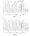
- FIG. 17is a schematic diagram illustrating a memory in accordance with another embodiment of the present invention.
- FIG. 18is a cross-sectional view of a portion of the memory illustrated in FIG. 17 in accordance with an embodiment of the present invention.
- FIG. 19is a diagram illustrating a current-voltage characteristic of a memory cell.
- FIG. 20is a block diagram illustrating a portion of a system in accordance with an embodiment of the present invention.
- Phase change memory devicesuse phase change materials, i.e., materials that may be electrically switched between a generally amorphous and a generally crystalline state, for electronic memory application.
- phase change materialsi.e., materials that may be electrically switched between a generally amorphous and a generally crystalline state
- One type of memory elementutilizes a phase change material that may be, in one application, electrically switched between a structural state of generally amorphous and generally crystalline local order or between different detectable states of local order across the entire spectrum between completely amorphous and completely crystalline states.
- the state of the phase change materialsare also non-volatile in that, when set in either a crystalline, semi-crystalline, amorphous, or semi-amorphous state representing a resistance value, that value is retained until changed by another programming event, as that value represents a phase or physical state of the material (e.g., crystalline or amorphous).
- a transistor or a diodemay be connected to the phase change material and may serve as a select device to access the phase change material during programming or read operations.
- the transistor or diodeis typically formed in or on the top surface of a silicon single crystal substrate.
- Transistorsmay take up a relatively large portion of the memory chip, and therefore may increase the memory cell size, thereby adversely affecting the memory capacity and cost/bit of a memory chip.
- Coupledmay mean that two or more elements are in direct physical or electrical contact. However, “coupled” may also mean that two or more elements are not in direct contact with each other, but yet still co-operate or interact with each other.
- Memory 100may include a 3 ⁇ 3 array of memory cells 111 - 119 , wherein memory cells 111 - 119 each include a select device 120 and a memory element 130 . Although a 3 ⁇ 3 array is illustrated in FIG. 1, the scope of the present invention is not limited in this respect. Memory 100 may have a larger array of memory cells.
- memory elements 130may comprise a phase change material.
- memory 100may be referred to as a phase change memory.
- a phase change materialmay be a material having electrical properties (e.g. resistance, capacitance, etc.) that may be changed through the application of energy such as, for example, heat, light, voltage potential, or electrical current.
- Examples of a phase change materialmay include a chalcogenide material or an ovonic material.
- An ovonic materialmay be a material that undergoes electronic or structural changes and acts as a semiconductor when subjected to application of a voltage potential, an electrical current, light, heat, etc.
- An ovonic materialmay be used in a memory element or in an electronic switch.
- a chalcogenide materialmay be a material that includes at least one element from column VI of the periodic table or may be a material that includes one or more of the chalcogen elements, e.g., any of the elements of tellurium, sulfur, or selenium.
- Memory 100may include column lines 141 - 143 and row lines 151 - 153 to select a particular memory cell of the array during a write or read operation.
- Column lines 141 - 143 and row lines 151 - 153may also be referred to as address lines since these lines may be used to address memory cells 111 - 119 during programming or reading.
- Column lines 141 - 143may also be referred to as bit lines and row lines 151 - 153 may also be referred to as word lines.
- Memory elements 130may be connected to row lines 151 - 153 and may be coupled to column lines 141 - 143 via select devices 120 . Therefore, when a particular memory cell (e.g., memory cell 115 ) is selected, voltage potentials may be applied to the memory cell's associated column line (e.g., 142 ) and row line (e.g., 152 ) to apply a voltage potential across the memory cell.
- a particular memory celle.g., memory cell 115
- voltage potentialsmay be applied to the memory cell's associated column line (e.g., 142 ) and row line (e.g., 152 ) to apply a voltage potential across the memory cell.
- Select device 120may be used to access memory element 130 during programming or reading of memory element 130 .
- Select device 120may operate as a switch that is either “off” or “on” depending on the amount of voltage potential applied across the memory cell.
- the off statemay be a substantially electrically nonconductive state and the on state may be a substantially conductive state.
- select device 120may have a threshold voltage and if a voltage potential less than the threshold voltage of select device 120 is applied across select device 120 , then select device 120 may remain “off” or in a relatively high resistive state so that little or no electrical current passes through the memory cell.
- select device 120may “turn on,” i.e., operate in a relatively low resistive state so that electrical current passes through the memory cell.
- select device 120may be in a substantially electrically nonconductive state if less than a predetermined voltage potential, e.g., the threshold voltage, is applied across select device 120 .
- Select device 120may be in a substantially conductive state if greater than the predetermined voltage potential is applied across select device 120 .
- Select device 120may also be referred to as an access device, an isolation device, or a switch.
- select device 120may comprise a switching material such as, for example, a chalcogenide or an ovonic material, and may be referred to as an ovonic threshold switch, or simply an ovonic switch.
- the switching material of select device 120may be a material in a substantially amorphous state positioned between two electrodes that may be repeatedly and reversibly switched between a higher resistance “off” state (e.g., greater than about ten mega-ohms) and a relatively lower resistance “on” state (e.g., about zero ohms) by application of a predetermined electrical current or voltage potential.
- select device 120may be a two terminal device that may have a current-voltage (I-V) characteristic similar to a phase change memory element that is in the amorphous state.
- the switching material of select device 120may not change phase. That is, the switching material of select device 120 may not be a programmable material, and as a result, select device 120 may not be a memory device capable of storing information.
- the switching material of select device 120may remain permanently amorphous and the I-V characteristic may remain the same throughout the operating life.
- An example of an I-V characteristic of select device 120is shown in FIG. 2 .
- select device 120in the low voltage or low electric field mode, i.e., where the voltage applied across select device 120 is less than a threshold voltage (labeled V TH ), select device 120 may be “off” or nonconducting, and exhibit a relatively high resistance, e.g., greater than about 10 mega-ohms. Select device 120 may remain in the off state until a sufficient voltage, e.g., V TH , is applied, or a sufficient current is applied, e.g., I TH , that may switch select device 120 to a conductive, relatively low resistance on state.
- V THthreshold voltage
- Snapbackmay refer to the voltage difference between V TH and V H of a select device.
- select device 120In the on state, the voltage potential across select device 120 may remain close to the holding voltage of V H as current passing through select device 120 is increased. Select device 120 may remain on until the current through select device 120 drops below a holding current, labeled I H . Below this value, select device 120 may turn off and return to a relatively high resistance, nonconductive off state until the V TH and I TH are exceeded again.
- select device 120may have a threshold voltage (V TH ) of about 5.3 volts, a holding voltage (V TH ) of about 0.8 volts, a threshold current (I TH ) of about 4 nano-amps, and a holding current (I H ) of about 100 nano-amps.
- V THthreshold voltage
- V THholding voltage
- I THthreshold current
- I Hholding current
- the snapbackmay be less than the V TH of the series memory element to avoid the possibility of read disturb if the snapback exceeds V TH of the memory element, encouraging it to turn on and drive the capacitance of the column and row lines, adversely passing current which could reduce the resistance of the memory element when the memory element is in the reset state.
- FIG. 3illustrates an embodiment of select device 120 .
- select device 120may include a bottom electrode 210 and a switching material 220 overlying bottom electrode 210 .
- switching material 220may be formed over and contacting bottom electrode 210 .
- select device 120may include a top electrode 230 overlying switching material 220 .
- bottom electrode 210may be a thin film material having a film thickness ranging from about 20 Angstroms ( ⁇ ) to about 2000 ⁇ . In one embodiment, the thickness of electrode 210 may range from about 100 ⁇ to about 1000 ⁇ . In another embodiment, the thickness of electrode 210 may be about 300 ⁇ .
- Suitable materials for bottom electrode 210may include a thin film of titanium (Ti), titanium nitride (TiN), titanium tungsten (TiW), carbon (C), silicon carbide (SiC), titanium aluminum nitride (TiAIN), titanium silicon nitride (TiSiN), polycrystalline silicon, tantalum nitride (TaN), some combination of these films, or other suitable conductors or resistive conductors compatible with switching material 220 .
- switching material 220may be a thin film material having a thickness ranging from about 20 ⁇ to about 2000 ⁇ . In one embodiment, the thickness of switching material 220 may range from about 200 ⁇ to about 1000 ⁇ . In another embodiment, the thickness of switching material 220 may be about 500 ⁇ .
- Switching material 220may be formed overlying bottom electrode 210 using a thin film deposition technique such as, for example, a chemical vapor deposition (CVD) process or a physical vapor deposition (PVD).
- Switching material 220may be a thin film of a chalcogenide material or an ovonic material in a substantially amorphous state that may be repeatedly and reversibly switched between a higher resistance “off” state and a relatively lower resistance “on” state by application of a predetermined electrical current or voltage potential.
- Switching material 220may not be a programmable material capable of storing information. In other words, switching material 220 may be a nonprogammable material.
- switching material 220may comprise a chalcogen other than oxygen.
- switching material 220may comprise tellurium and/or selenium.
- switching material 220may comprise silicon (Si), tellurium (Te), arsenic (As), and germanium (Ge), or combinations of these elements.
- a composition for switching material 220may include an alloy of silicon (Si), tellurium (Te), arsenic (As), germanium (Ge), and indium (In) or an alloy of Si, Te, As, Ge, and phosphorous (P).
- the composition of switching material 220may comprise a Si concentration of about 14%, a Te concentration of about 39%, an As concentration of about 37%, a Ge concentration of about 9%, and an In concentration of about 1%.
- the composition of switching material 220may comprise a Si concentration of about 14%, a Te concentration of about 39%, an As concentration of about 37%, a Ge concentration of about 9%, and a P concentration of about 1%.
- the percentagesare atomic percentages which total 100% of the atoms of the constituent elements.
- a composition for switching material 220may include an alloy of arsenic (As), tellurium (Te), sulfur (S), germanium (Ge), selenium (Se), and antimony (Sb) with respective atomic percentages of 10%, 21%, 2%, 15%, 50%, and 2%.
- switching material 220may include Si, Te, As, Ge, sulfur (S), and selenium (Se).
- the composition of switching material 220may comprise a Si concentration of about 5%, a Te concentration of about 34%, an As concentration of about 28%, a Ge concentration of about 11%, a S concentration of about 21%, and a Se concentration of about 1%.
- Top electrode 230may be a thin film material having a thickness ranging from about 20 angstroms ( ⁇ ) to about 2000 ⁇ . In one embodiment, the thickness of electrode 230 may range from about 100 ⁇ to about 1000 ⁇ . In another embodiment, the thickness of electrode 230 may be about 300 ⁇ .
- Suitable materials for top electrode 230may include a thin film of titanium (Ti), titanium nitride (TiN), titanium tungsten (TiW), carbon (C), silicon carbide (SiC), titanium aluminum nitride (TiAIN), titanium silicon nitride (TiSiN), polycrystalline silicon, tantalum nitride (TaN), some combination of these films, or other suitable conductors or resistive conductors compatible with switching material 220 .
- top electrode and bottom electrodemay comprise carbon and may have a thickness of about 500 ⁇ .
- Top electrode 230may also be referred to as an upper electrode and bottom electrode 210 may also be referred to as a lower electrode.
- select device 120may be referred to as a vertical structure since electrical current may flow vertically through switching material 220 between top electrode 230 and bottom electrode 210 .
- Select device 120may be referred to as a thin film select device if thin films are used for switching material 220 and electrodes 210 and 230 .
- the threshold current (I TH ) of select device 120may be less than the threshold current for an ovonic memory device set in a high resistance, amorphous state.
- the threshold voltage (V TH ) of select device 120may be altered by changing process variables such as, for example, the thickness or alloy composition of switching material 220 . For example, increasing the thickness of switching material 220 may increase the threshold voltage of select device 120 .
- the holding voltage (V H ) of select device 120may be altered or set by the type of contact to switching device 120 , e.g., the composition of electrodes 210 and 230 may determine the holding voltage of select device 120 .
- the threshold voltage of select device 120may be about two volts and the holding voltage of select device 120 may be about one volt.
- the threshold voltage of select device 120may be about 0.8 volts.
- the holding voltage of select device 120may be about 0.4 volts.
- the holding voltage of select device 120may be about 0.15 volts.
- Select device 120may provide a relatively high “on current” for a given area of a device compared to other switching devices such as, for example, metal-oxide-semiconductor (MOS) transistors or bipolar junction transistors (BJTs).
- MOSmetal-oxide-semiconductor
- BJTsbipolar junction transistors
- the relatively higher on current of select device 120 in the on statemay allow for a relatively higher programming current available to select device 120 to program a memory element (e.g., 130 ).
- the memory array shown in FIG. 1 using select device 120 illustrated in FIG. 3may be constructed by stacking select device 120 and memory element 130 in a vertical configuration.
- An example of a vertical structure comprising select device 120 formed over memory element 130is illustrated in FIG. 4 .
- Memory 100may comprise a substrate 240 , an insulating material 260 overlying substrate 240 , and a conductive material 270 overlying insulating material 260 .
- Conductive material 270may be an address line (e.g., row line 152 ).
- an opening(not shown in FIG. 4) may be formed in an insulating material 280 . In the opening, a lower electrode 340 may be formed.
- Conductive material 380may be an address line (e.g., column line 142 ).
- memory material 350 and electrodes 340 and 360may form memory element 130 .
- memory material 350is an ovonic material or a chalcogenide material
- memory element 130may be referred to as a phase change memory device or an ovonic memory device.
- select device 120is formed over memory element 130 to form a vertical structure or a vertical stack.
- memory element 130may be formed above select device 120 to form a vertical structure.
- select device 120 and memory element 130are formed using only thin film materials, and the vertical stack may be referred to as a thin film vertical stack.
- a thin film materialmay be a particular class of insulating or conducting material deposited onto a substrate or other materials and may have a specified thickness, e.g., thin film materials may refer to materials having a thickness ranging from greater than zero ⁇ to less than about 25,000 ⁇ .
- thin film materialsmay be materials deposited using thin film deposition techniques such as, for example, PVD (Physical Vapor Deposition), CVD (Chemical Vapor Deposition), or PECVD (Plasma Enhanced Chemical Vapor Deposition), etc.
- barrier material 370may be eliminated from the vertical structure.
- barrier material 370may be eliminated from the vertical structure and electrode 360 may be combined with electrode 210 into a single conductive layer to form a single electrode.
- electrode 230may be combined with conductive material 380 to form a single conductive layer or single electrode.
- Memory material 350may be a phase change, programmable material capable of being programmed into one of at least two memory states by applying a current to memory material 350 to alter the phase of memory material 350 between a substantially crystalline state and a substantially amorphous state, wherein a resistance of memory material 350 in the substantially amorphous state is greater than the resistance of memory material 350 in the substantially crystalline state.
- Programming of memory material 350 to alter the state or phase of the materialmay be accomplished by applying voltage potentials to conductive materials 380 and 270 , thereby generating a voltage potential across select device 120 and memory element 130 .
- the voltage potentialis greater than the threshold voltages of select device 120 and memory element 130 , then an electrical current may flow through memory material 350 in response to the applied voltage potentials, and may result in heating of memory material 350 .
- This heatingmay alter the memory state or phase of memory material 350 .
- Altering the phase or state of memory material 350may alter the electrical characteristic of memory material 350 , e.g., the resistance of the material may be altered by altering the phase of the memory material 350 .
- Memory material 350may also be referred to as a programmable resistive material.
- memory material 350may be in an amorphous or semi-amorphous state and in the “set” state, memory material 350 may be in an a crystalline or semi-crystalline state.
- the resistance of memory material 350 in the amorphous or semi-amorphous statemay be greater than the resistance of memory material 350 in the crystalline or semi-crystalline state.
- memory material 350may be heated to a relatively higher temperature to amorphosize memory material 350 and “reset” memory material 350 (e.g., program memory material 350 to a logic “0” value). Heating the volume of memory material 350 to a relatively lower crystallization temperature may crystallize memory material 350 and “set” memory material 350 (e.g., program memory material 350 to a logic “1” value).
- Various resistances of memory material 350may be achieved to store information by varying the amount of current flow and duration through the volume of memory material 350 .
- Memory 100 shown in FIG. 4may be referred to as a vertical phase change memory structure since current may flow vertically between address lines through select device 120 and memory element 130 .
- memory 100may be arranged differently and include additional layers and structures. For example, it may be desirable to form isolation structures, peripheral circuitry (e.g., addressing circuitry), transistors in substrate 240 , etc. It should be understood that the absence of these elements in the drawings is not a limitation of the scope of the present invention.
- the memory structure illustrated in FIG. 4does not use transistor or diode select devices.
- the memory structure illustrated in FIG. 4may be constructed as a standalone array or arrays on a substrate or may be constructed as a process module inserted into a more complex process flow that builds other structures.
- this modulemay be integrated into a full complementary metal-oxide-semiconductor (CMOS) process that may also build N-channel and P-channel transistors, their wiring interconnects, and other circuit elements.
- CMOScomplementary metal-oxide-semiconductor
- the row and column linesmay be respectively driven by N and P channel transistors for reading and writing in ways apparent to one reasonably skilled in the art.
- a “half select array biasing scheme”may be implemented, wherein a voltage of, for example, V volts, may be applied to the selected column line (e.g., 142 ) and approximately zero volts may be applied to the selected row line (e.g., 152 ).
- Vmay be chosen to be greater than the threshold voltage of select device 120 (V TH SD)+the reset threshold voltage of memory element 130 (V TH Reset), but less than two times V TH SD. In other words (V TH SD+V TH Reset) ⁇ V ⁇ (2*V TH SD). All unselected rows and columns may be biased at V/2. In this approach, there may be no voltage bias between unselected row lines and unselected column lines. This may reduce background leakage current.
- memory elements of the arraymay be programmed by successively forcing a current sufficient in magnitude and with a fast falling edge of less than about 5 nano-seconds for reset and slow falling edge greater than about 200 nano-seconds for the set state to change phase of the memory material
- Vmay be chosen to be greater than the threshold voltage of select device 120 (V TH SD), but less than the threshold voltage of select device 120 (V TH SD)+the reset threshold voltage of memory element 130 (V TH Reset). In other words (V TH SD) ⁇ V ⁇ (V TH SD+V TH Reset). All unselected rows and unselected columns may be biased at V/2. In this approach, there may be no voltage bias between unselected row lines and unselected column lines. This may reduce background leakage current. After biasing the memory array in this way, memory elements of the array may be successively read by successively forcing a relatively lower current or voltage than that required to write or disturb a bit, to determine resistance of the memory material of the memory elements.
- a forced voltageis less than the voltage that will exceed the threshold of the memory element yet great enough to result in detectably more current through a set bit than a reset bit.
- a current less than I TH of the memory elementmay be forced through a bit. This current may cause a detectably smaller voltage drop across a set memory element than a reset memory element.
- the reset currentmay be about 1.5 miliamps (ma) and I TH may be greater than about 0.03 ma.
- Ireadmay be about 0.01 ma for a process with Rset less than about 10,000 ohms, so that the maximum drop across a set memory element may be under about 0.1 volts and I TH of the memory element is not exceeded.
- the reset devicemay clamp the voltage across the memory device at about 0.6 volts without thresholding or snapping back. This will provide a read voltage difference between the set and reset state of about 0.6 volts minus about 0.1 or 0.5 volts, that may accommodate the variation in the hold voltages of the device switch and memory element.
- Vmay be chosen to be greater than the threshold voltage of select device 120 (V TH SD)+the reset threshold voltage of memory element 130 (V TH Reset), but less than three times V TH SD. In other words (V TH SD+V TH Reset) ⁇ V ⁇ (3*V TH SD). All unselected rows may be biased at (2V)/3. All unselected columns may be biased at V/3.
- a voltage of Vmay be chosen to be greater than the threshold voltage of select device 120 (V TH SD), but less than the threshold voltage of select device 120 (V TH SD)+the reset threshold voltage of memory element 130 (V TH Reset). In other words (V TH SD) ⁇ V ⁇ (V TH SD+V TH Reset). All unselected rows may be biased at (2V)/3. All unselected columns may be biased at V/3. In this approach, there may be a voltage bias between unselected row lines and unselected column lines of approximately +/ ⁇ V/3. This may provide additional manufacturing margin for variability of threshold voltage of select device 120 . After biasing the memory array in this manner, memory elements of the array may be read by forcing a relatively lower current to determine resistance of the memory material of the memory elements such as by the methods used in the V/2 approach discussed above in the half select approach.
- Programming a selected memory cellmay include biasing unselected row and unselected column lines as discussed above in the “half select array biasing scheme” and “one-third select array biasing scheme” embodiments.
- a currentOn the selected column line, a current may be forced with a compliance that may be greater than the threshold voltage of selected device 120 and the threshold voltage of memory element 130 .
- the current amplitude, duration, and pulse shapemay be selected to place the memory element in the desired phase or memory state.
- Reading a selected memory cell of the arraymay include biasing unselected row and column lines as discussed above in the “half select array biasing scheme” and “one-third select array biasing scheme” embodiments. Combinations of these schemes for conventional use that reflect margin needs, array sizes, and leakage requirements in the product may allow one reasonably skilled in the art to determine the appropriate bias voltages that will meet product specifications which may vary by application. Zero volts may be applied to the selected row line and a voltage V applied on the selected column line. The current compliance of this forced voltage may be less than the current that may program or disturb the present phase or memory state of the memory element. If the memory element is in a “reset” state, the memory element may not switch “on” and may present a relatively large voltage, low current condition to a sense amplifier (not shown). The sense amplifier may either compare the resulting column voltage to a reference voltage or compare the resulting column current to a reference current.
- FIGS. 5-12may be used to illustrate an embodiment to fabricate or manufacture a portion of memory 100 .
- FIGS. 5-12may be used to illustrate an embodiment to fabricate select device 120 and memory element 130 .
- memory 100may comprise a substrate 240 that may be, for example, a semiconductor substrate (e.g., a silicon substrate), although the scope of the present invention is not limited in this respect.
- a substrate 240may be, for example, a semiconductor substrate (e.g., a silicon substrate), although the scope of the present invention is not limited in this respect.
- Other suitable substratesmay be, but are not limited to, substrates that contain ceramic material, organic material, or a glass material.
- Insulating material 260may be a dielectric material that may be a thermally and/or electrically insulating material such as, for example, silicon dioxide, although the scope of the present invention is not limited in this respect. Insulating material 260 may have a thickness ranging from about 300 ⁇ to about 10,000 ⁇ , although the scope of the present invention is not limited in this respect. Insulating material 260 may be planarized using a chemical or chemical-mechanical polish (CMP) technique.
- CMPchemical or chemical-mechanical polish
- a thin film of a conductive material 270may be formed overlying insulating material 270 using, for example, a PVD process.
- Conductive material 270may be patterned using photolithographic and etch techniques to form a small width in the y-direction (orthogonal to the view shown in FIG. 5 ).
- the film thickness of conductive material 270may range from about 20 ⁇ to about 2000 ⁇ . In one embodiment, the thickness of conductive material 270 may range from about 200 ⁇ to about 1000 ⁇ . In another embodiment, the thickness of conductive material 270 may be about 500 ⁇ .
- Conductive material 270may be an address line of memory 100 (e.g., row line 151 , 152 , or 153 ).
- Conductive material 270may be, for example, a tungsten (W) film, a doped polycrystalline silicon film, a Ti film, a TiN film, a TiW film, an aluminum (Al) film, a copper (Cu) film, or some combination of these films.
- conductive material 270may be a polycrystalline silicon film with a resistance lowering strap of a refractory silicide on its top surface, similar to a poly gate used in CMOS over a thick filed oxide, although the scope of the present invention is not limited in this respect.
- An insulating material 280may be formed overlying conductive material 270 using, for example, a PECVD (Plasma Enhanced Chemical Vapor Deposition) process, HDP (High Density Plasma) process, or spin-on and bake SOLGEL process.
- Insulating material 280may be a dielectric material that may be a thermally and/or electrically insulating material such as, for example, silicon dioxide, although the scope of the present invention is not limited in this respect.
- Insulating material 280may have a thickness ranging from about 100 ⁇ to about 4000 ⁇ , although the scope of the present invention is not limited in this respect. In one embodiment, the thickness of insulating material 280 may range from about 500 ⁇ to about 2500 ⁇ . In another embodiment, the thickness of insulating material 280 may be about 1200 ⁇ .
- insulating material 280may be planarized using a chemical or CMP technique.
- the resulting thickness of insulating material 280may range from about 20 ⁇ to about 4000 ⁇ .
- the thickness of insulating material 280may range from about 200 ⁇ to about 2000 ⁇ .
- the thickness of insulating material 280may be about 900 ⁇ .
- a sacrificial film 410may be deposited overlying insulating material 280 .
- Sacrificial film 410may be, for example, a silicon nitride (SiN) film or a polycrystalline silicon film.
- the thickness of sacrificial film 410may range from about 20 ⁇ to about 4000 ⁇ . In one embodiment, the thickness of sacrificial film 410 may range from about 200 ⁇ to about 2000 ⁇ . In another embodiment, the thickness of sacrificial film 410 may be about 1000 ⁇ .
- Sacrificial film 410may be patterned using photolithographic and etch techniques to form openings 415 having sidewalls 416 .
- Openings 415may be holes, vias or trenches, although the scope of the present invention is not limited in this respect.
- openings 415may be formed using photolithographic and etch techniques.
- openings 415may be formed by applying a layer of photoresist material (not shown) on sacrificial film 410 and exposing this photoresist material to light.
- a mask(not shown) may be used to expose selected areas of the photoresist material, which defines areas to be removed, i.e., etched.
- the etchmay be a chemical etch, which may be referred to as a wet etch.
- the etchmay be a plasma (ion bombardment) etch, which may be referred to as a dry etch.
- the diameter or width of openings 415may be at least one minimum feature size.
- the minimum feature size of a structuremay refer to the minimum dimension achievable using photolithography.
- the minimum feature sizemay refer to a width of a material or spacing of materials in a structure.
- photolithographyrefers to a process of transferring a pattern or image from one medium to another, e.g., as from a mask to a wafer, using a certain wavelength or wavelengths of light.
- the minimum feature size of the transferred pattern that is available in state of the art IC manufacturingmay be limited by the limitations of the wavelength of the light source.
- Distances, sizes, or dimensions less than the minimum feature sizemay be referred to as sub-lithographic distances, sizes, or dimensions.
- some photolithographic processesmay have minimum feature sizes of about 2500 angstroms.
- a sub-lithographic distancemay refer to a feature having a width of less than about 2500 angstroms.
- Electron beam lithographymay refer to a direct-write lithography technique using a beam of electrons to expose resist on a wafer.
- X-ray lithographymay refer to an advanced lithographic process for transferring patterns to a silicon wafer in which the electromagnetic radiation used is X-ray, rather than longer wavelength radiation.
- the shorter wavelength for X-raysmay reduce diffraction, and may be used to achieve feature sizes of about 1000 angstroms and less.
- sidewall spacersmay be used to achieve sub-lithographic dimensions.
- FIG. 6may be used to illustrate the use of sidewall spacers 420 to achieve sub-lithographic dimensions.
- FIG. 6depicts the structure of FIG. 5, through the same cross-sectional view, after forming sidewall spacers 420 .
- sidewall spacers 420may be formed along sidewalls 416 of a sacrificial film 410 .
- the distance between sidewalls 416may be one feature size and may be formed using photolithographic and etch techniques.
- Sidewall spacers 420may be formed by depositing a layer of silicon nitride, poly silicon, or another sacrificial material in the space between sidewalls 416 and patterning this material using a dry etch such as, for example, an anisotropic etch.
- the distance between sidewall spacers 420may be sub-lithographic. After sidewall spacers 420 are formed, in one embodiment, another anisotropic etch may be used to form an opening 430 (FIG. 7) in thin film 280 having a sub-lithographic diameter.
- sacrificial film 410 and spacers 420may be used as a hard mask and insulating material 280 may be anisotropically etched using an etching agent that is selective such that the etching agent stops at, or preserves, conductive material 270 .
- the etching operationexposes a portion of conductive material 270 through opening 430 .
- sidewall spacers 420may serve to reduce the quantity of electrode material (e.g., 340 shown in FIG. 8) formed in opening 430 .
- the diameter of opening 430may be less than about 1000 angstroms, although the scope of the present invention is not limited in this respect.
- opening 430is not a limitation of the present invention.
- Other sub-lithographic methodsmay be used to form opening 430 , wherein opening 430 may have a sub-lithographic diameter.
- opening 430may be formed using photolithographic techniques and may therefore, have a diameter of greater than or equal to about one minimum feature size.
- Sacrificial film 410 and spacers 420may be removed after forming opening 430 .
- sacrificial film 410 and spacers 420may be selectively etched while preserving insulating material 280 and conductive material 270 .
- FIG. 8illustrates memory 100 after the conformal deposition of an electrode material 340 over insulating material 280 and in opening 430 (FIG. 7 ).
- Electrode material 340may be a layer of C, SiC, TiSIN, TIAIN, polycrystalline silicon, TaN, some combination of these, or other suitable resistive conductors.
- electrode material 340may be formed using a chemical vapor deposition (CVD) process, however, the scope of the present invention is not limited by the particular process used to form electrode material 340 . It should also be understood that alternative processes may be used to form electrode material 340 . As an example, ALD (Atomic Layer Deposition) may be used.
- CVDchemical vapor deposition
- FIG. 8may be subjected to a planarization that removes a portion of electrode material 340 and may remove a portion of insulating layer 280 .
- Suitable planarization techniquesmay include a chemical or CMP technique. Other techniques may also be used to pattern materials 340 and 280 . For example, a blanket etch may be used to remove portions of insulating layer 280 and electrode material 340 .
- FIG. 9illustrates the structure shown in FIG. 8 after patterning of electrode material 340 .
- FIG. 10illustrates the structure of FIG. 9 at a later stage of fabrication.
- a thin film of memory material 350may be deposited overlying insulating material 280 and electrodes 340 .
- Memory material 350may be formed using, for example, a PVD process.
- Memory material 350may be a programmable material such as, for example, a phase change material.
- Memory material 350may be an ovonic material or a chalcogenide material.
- the thickness of memory material 350may range from about 20 ⁇ to about 4000 ⁇ . In one embodiment, the thickness of memory material 350 may range from about 200 ⁇ to about 1000 ⁇ . In another embodiment, the thickness of memory material 350 may be about 500 ⁇ .
- Electrode material 360may be deposited overlying memory material 350 . Electrode material 360 may be formed using, for example, a PVD process. Electrode material 360 may be Ti, TiN, TiW, C, SiC, TIAIN, TiSiN, polycrystalline silicon, TaN, some combination of these, or other suitable conductors or resistive conductors. The thickness of electrode material 360 may range from about 20 ⁇ to about 2000 ⁇ . In one embodiment, the thickness of electrode material 360 may range from about 100 ⁇ to about 1000 ⁇ . In another embodiment, the thickness of electrode material 360 may be about 300 ⁇ .
- Barrier material 370may be deposited overlying electrode material 360 .
- Barrier material 370may be formed using, for example, a PVD process.
- Barrier material 370may be Ti, TiN, TiW, C, SiC, TIAIN, TiSiN, polycrystalline silicon, TaN, some combination of these, or other suitable conductors or resistive conductors that provide a barrier between electrode materials 360 and 210 .
- barrier materialmay be composed of TiN and Ti films.
- the thickness of barrier material 370may range from about 20 ⁇ to about 2000 ⁇ . In one embodiment, the thickness of barrier material 370 may range from about 100 ⁇ to about 1000 ⁇ . In another embodiment, the thickness of barrier material 370 may be about 300 ⁇ .
- Electrode 210may be deposited overlying barrier material 370 using, for example, a PVD process.
- Switching material 220may be deposited overlying electrode 210 using, for example, a PVD process and electrode 230 may be deposited overlying switching material 220 using, for example, a PVD process. Examples of compositions and thicknesses of electrode 210 , switching material 220 , and electrode 230 are discussed above with reference to FIG. 3 .
- thin film layers 350 , 360 , 370 , 210 , 220 , and 230 or a subset thereofmay be deposited by means of a PVD process, in-situ. That is, all layers may be deposited sequentially in a sputter deposition tool without venting back to atmospheric pressure or exposure to atmospheric gases between each thin film layer deposition.
- FIG. 11illustrates the structure shown in FIG. 10 after patterning of materials 230 , 220 , 210 , 370 , 360 , and 350 using, for example, photolithographic and etch techniques, to form three cylindrical or box structures 500 .
- Cylinder shaped structuresmay be achieved using a single photo/single etch process.
- Box shaped structuresmay be achieved using a dual photo/single etch process.
- box shaped structuresmay be achieved using a single photo/single etch/single photo/single etch process.
- three cylindrical or box structuresare illustrated, this is not a limitation in the present invention. For example, in other embodiments, more than three cylinder or box shaped structures may be formed.
- FIG. 11illustrates memory 100 after the conformal deposition of an insulating material 510 on a portion of a top surface of insulating material 280 , and along the sidewalls and top surface of structures 500 .
- Insulating material 510may be a silicon dioxide or silicon nitride material.
- Insulating material 510may have a thickness ranging from about 20 ⁇ to about 10,000 ⁇ . In one embodiment, the thickness of insulating material 510 may range from about 100 ⁇ to about 1000 ⁇ . In another embodiment, the thickness of insulating material 510 may be about 250 ⁇ .
- Insulating material 510may be deposited at a relative cooler temperature, e.g., in the range of 200-600 degrees Celsius, and in one embodiment, at a temperature of about 250 degrees Celsius.
- Interlayer insulator 520may be deposited overlying insulating material 510 .
- Interlayer insulator 520may be, for example, a silicon dioxide deposited using a high density plasma (HDP) process.
- Interlayer insulator 520may have a thickness ranging from about 300 ⁇ to about 20,000 ⁇ . In one embodiment, the thickness of interlayer insulator 520 may range from about 2000 ⁇ to about 10,000 ⁇ . In another embodiment, the thickness of interlayer insulator 520 may be about 6000 ⁇ .
- FIG. 12illustrates the structure shown in FIG. 11 after planarization of materials 510 , 520 , and possibly 230 using, for example, a CMP process.
- Conductive materials 380may be formed over and contacting electrodes 230 by, for example, depositing a layer of aluminum and patterning this layer using photolithographic and etch techniques to form parallel strips that extend in the y-direction (orthogonal to the x-direction shown in FIG. 12 ).
- Conductive materials 380may be address lines such as, for example, column lines 141 - 143 schematically illustrated in FIG. 1 . As may be appreciated, column lines 141 - 143 may be orthogonal to row lines 151 - 153 .
- conductive layer 380may include a tungsten (W) film, a doped polycrystalline silicon film, a Ti film, a TiN film, a TiW film, a copper film, or some combination of these films.
- conductive material 380may be a polycrystalline silicon film with a resistance lowering strap of a cobalt silicide (CoSi 2 ) on its top surface.
- Conductive material 380may have a thickness ranging from about 100 ⁇ to about 20,000 ⁇ . In one embodiment, the thickness of conductive material 380 may range from about 300 ⁇ to about 5000 ⁇ . In another embodiment, the thickness of conductive material 380 may be about 2000 ⁇ .
- memory material 350 and electrodes 340 and 360may form memory element 130 (FIG. 1 ).
- Switching material 220 and electrodes 210 and 230may form select device 120 (FIG. 1 ).
- FIG. 12illustrates an example of a four layer stack of memory arrays in accordance with an embodiment of the present invention.
- on-chip transistors, peripheral circuitry, and/or address circuitrymay be positioned under the memory array. This may reduce chip die area.
- Memory array efficiencymay be defined as the percentage of the total product chip area that is made up of memory cells compared to the amount of chip area that is used for other circuitry. In one embodiment, memory efficiency of 90% or higher may be achieved by using the thin film memory structures as discussed above along with placing on-chip transistors, peripheral circuitry, and/or address circuitry underneath the memory array. Alternately, SRAM may be placed under the memory array in available places to increase the bandwidth of writing to the chip for later data placement in the non-volatile memory portion of the chip.
- Stacked multi-layer arraysmay gain access to on chip CMOS transistor pitched array support subcircuits such as, for example, row drivers, column drivers, and sense-amps, as schematically illustrated in FIG. 14 .
- CMOS transistor pitched array support subcircuitssuch as, for example, row drivers, column drivers, and sense-amps, as schematically illustrated in FIG. 14 .
- FIG. 14a memory 600 is illustrated.
- Memory 600may include memory cells 630 coupled between row lines 610 and column lines 620 which may run orthogonal to row lines 610 .
- Memory cells 630may include a vertically stacked, thin film select device and a memory element such as a phase change memory element as discussed herein.
- memory cells 630may include a vertical structure that includes a select device and a memory element such as a phase change memory element that are formed using thin film materials.
- Support subcircuits 640may be under memory cells 630 and may be coupled to row lines 610 and column lines 620 . These subcircuits may comprise drive and sense transistors for the array, and also other support circuits helpful for efficient use of the memory in a system such as, for example, cache SRAM memory. Placing support subcircuits 640 under the memory array in this manner may increase memory efficiency and may economically allow fewer bits per row line and per column line. This may have the advantage of increasing speed for read and write operations due to reduced parasitic resistance and capacitance and may also provide for more efficient redundancy schemes.
- FIG. 15illustrates another embodiment of memory 100 .
- a row lineis formed using a salicided single crystal active region of N+ or P+.
- a row linemay be formed using a P region 720 , an N+ region 730 , and a refractory salicide strap 740 of, for example, CoSi 2 , TiSi 2 , or NiSi 2 .
- This row linemay be coupled to electrodes 340 via conductive plugs 710 .
- Conductive plugs 710may be surrounded by an insulating material 750 , such as, for example, a silicon dioxide.
- Conductive plugs 710may be, for example, tungsten, and may include a liner (not shown) of, for example, Ti and/or TiN.
- conductive material 380may be coupled to electrode 230 via a conductive plug.
- FIG. 16illustrates an alternate embodiment of a memory cell (e.g., 115 ) of memory 100 .
- memory cell 115may include an electrode 830 , a switching material 820 overlying electrode 830 , and an electrode 810 overlying switching material 820 to conduct current between the switching material 820 and memory material 850 .
- memory cell 115may include a memory material 850 overlying electrode 810 .
- electrode 810may be under and contacting memory material 850 .
- memory cell 115may include an electrode 840 overlying memory material 850 .
- Memory cell 115is a vertical structure that may be formed of thin film materials and may be formed over a substrate (not shown).
- Select device 120may include switching material 820 along with it's upper and lower electrodes 810 and 830 respectively, and memory element 130 may include memory material 850 along with it's upper and lower electrodes 840 and 810 , respectively.
- Switching material 820may be formed using the same or similar materials, and using the same or similar techniques as described herein for switching material 220 . Further, memory material 850 may be formed of the same or similar materials, and using the same or similar techniques as described herein for memory material 350 .
- Electrodes 830 and 840may serve as address lines (e.g., column or row lines). Electrodes 830 , 810 , and 840 may be composed of materials similar to, or the same as the examples discussed herein for materials 380 , 370 , 230 , 210 , 360 , and 340 . In one embodiment, electrodes 830 , 810 , and 840 may be a layer of carbon, although the scope of the present invention is not limited in this respect. In addition, the thickness of, and the techniques used to form materials 380 , 370 , 230 , 210 , 360 , and 340 may be used to form electrodes 830 , 810 , and 840 .
- FIG. 17is a schematic diagram illustrating another embodiment of memory 100 .
- memory cells 111 - 119each include select device 120 , a select device 125 , and memory element 130 .
- the total snapbackmay be reduced to allow use of a lower threshold memory element. For example, if the total V TH for the pair of ovonic switches is about two volts, the individual V TH of each switch may be about one volt by appropriate choice of the switching material thickness. If the V H of each is, for example, 0.8 volts, the snapback may be reduced to about 0.4 volts total from about 1.2 volts if a single device is used.
- Such a stacked series set of switch devicesmay reduce the tendency to disturb a bit during read.
- Such a stackmay be comprised of one switch, two switches, or more switches in series with the memory element, all placed between the row and column line assisting reliable memory selection and operation.
- select devices 120 and 125are connected in a serial arrangement.
- select devices 120 and 125may be ovonic switches and memory element 130 may be an ovonic memory.
- Memory cell 115may comprise substrate 240 , insulating material 260 overlying substrate 240 , and conductive material 270 overlying insulating material 260 .
- Conductive material 270may be an address line (e.g., row line 152 ).
- electrode 340may be formed between portions of insulating material 280 .
- Conductive material 980may be an address line (e.g., column line 142 ).
- the embodiment of memory cell 115 illustrated in FIG. 18may be formed using similar materials and manufacturing techniques as discussed with reference to FIGS. 5-12 and 15 .
- select devices 125 and 120are formed over memory element 130 to form a serially coupled, thin film vertical structure or vertical stack.
- memory element 130may be formed above select devices 120 and 125 or memory element 130 may be formed between select devices 120 and 125 to form a serially coupled, thin film vertical structure.
- select devices 120 and 125 and memory element 130may be formed using thin film materials, and the vertical stack may be referred to as a thin film vertical stack.
- memory material 350 and electrodes 340 and 360may form memory element 130 .
- Memory material 350may be an ovonic material or a chalcogenide material and may be referred to as an ovonic memory.
- Switching material 920 and electrodes 360 and 930may form select device 125 .
- Switching material 920may be formed using similar materials and similar manufacturing techniques used to form switching material 220 described herein.
- Switching material 940 and electrodes 930 and 950may form select device 120 .
- Switching material 940may be formed using similar materials and similar manufacturing techniques used to form switching material 220 described herein.
- switching materials 920 and 940may be composed of the same material or different materials.
- switching material 920may be composed of a chalcogenide material and switching material 940 may be composed of another different chalcogenide material.
- select devices 120 and 125may be ovonic switches and memory element 130 may be an ovonic memory and memory cell 115 may be referred to as an ovonic memory cell.
- I-V characteristic for select device 120is shown in FIG. 2 .
- Select device 125may have an I-V characteristic similar to that illustrated in FIG. 2 .
- FIG. 19an example of an I-V characteristic of memory cell 115 , which may include memory element 130 and select devices 120 and 125 in this embodiment, is shown.
- the holding voltage of memory cell 115labeled V H , may result from the holding voltages of select devices 120 and 125 and memory element 130 .
- the threshold voltage of memory cell 115may be equal to the combined threshold voltages of memory element 130 and select devices 120 and 125 .
- the threshold voltage of a select device or an ovonic switchmay be determined by the thickness or alloy composition of the switching material of the ovonic switch and the holding voltage of an ovonic switch may be determined by the composition of the electrodes contacting the switching material of the ovonic switch. Accordingly, in one embodiment, the snapback voltage, i.e., the voltage difference between the threshold and holding voltages of an ovonic switch, may be reduced by reducing the thickness of the switching material and using a particular type of electrode.
- the holding voltage of select device 120may be about one volt and the threshold voltage of select device 120 may be about 1.2 volts.
- the snapback voltagemay be about 0.2 volts, which is the difference between the holding and threshold voltages of select device 120 .
- memory cell 115may include two ovonic switches serially coupled to an ovonic memory to decrease the voltage difference between the holding voltage and the threshold voltage of a memory cell when higher switching and holding voltages are desired.
- two ovonic switchesmay be serially coupled to an ovonic memory to decrease “snapback” of a memory cell, i.e., reduce the voltage difference between the threshold and holding voltages of an ovonic memory cell when higher switching and holding voltages are desired.
- electrodes 360 , 930 , and 950may be carbon, the thickness of switching material 920 may be about 200 ⁇ , and the thickness of switching material 940 may be about 200 ⁇ .
- the threshold voltage of select device 120may be about 1.2 volts and the holding voltage of select device 120 may be about one volt.
- the threshold voltage of select device 125may be about 1.2 volts and the holding voltage of select device 125 may be about one volt. If the threshold voltage of reset/set memory element 130 is about 0.8/0.0 volts, then the threshold voltage of memory cell 115 may be about 3.2/2.4 volts for memory cell 115 in a reset state and set state, respectively, which is the combined threshold voltages of memory element 130 and select devices 120 and 125 .
- a voltage potential of greater than about 3.2 voltsmay be applied across memory cell 115 to “turn on” select devices 120 and 125 and conduct current through memory cell 115 .
- a voltage of greater than about 3.2 voltsmay be applied across memory cell 115 by applying a voltage potential of greater than about 3.2 volts to column line 142 and a voltage potential of about zero volts to row line 152 .
- a voltage of about 1.8 voltsmay be applied to unselected column and unselected row lines, e.g., lines 141 , 143 , 151 , and 153 .
- a voltage of greater than about 3.2 voltsmay be applied to a selected column line, e.g., 142 , and zero volts may be applied to a selected row line, e.g., row line 152 .
- the voltage drop across memory cell 115may be reduced from about 3.2 volts to about 2.0-2.8 volts depending on the cell's memory state and current provided by the column.
- informationmay be stored in memory element 130 by forcing current through memory cell 115 while assuring that the selected column line remains within about 2.4 volts of the unselected row lines biased at about 1.8 volts so that unselected memory cells are not disturbed. That is, the column may not be allowed to be higher than about 4.2 volts during programming.
- FIG. 19may be used to graphically illustrate this example, wherein for the full memory cell (all 3 components taken together), V TH is 3.2/2.4 volts for a reset state and set state, respectively, and V H is 2.8 volts.
- the current through memory cell 115is near zero amperes until the threshold voltage, V TH , of, for example, about 3.2 or 2.4 volts is exceeded, depending on whether the memory cell is in a reset or set state respectively. Then the voltage across memory cell 115 drops to (for a reset bit) or climbs to (for a set bit) the holding voltage, V H , of, for example, about 2.8 volts, as the current is increased.
- a voltage of about 2.8 voltsmay be applied across memory cell 115 .
- the resistance of memory element 130may be sensed to determine if memory element 130 is in a low resistance crystalline, “set” state (e.g., less than about 10,000 ohms) or if memory element 130 is in a high resistance amorphous, “reset” state (e.g., greater than about 10,000 ohms).
- a voltage of about 2.8 voltsmay be applied across memory cell 115 by applying 2.8 volts to the selected column and zero volts to the selected row and 1.4 volts to all other unselected rows and columns.
- the resistance from the selected column to the selected rowmay be sensed to determine if memory element 130 is in a low resistance crystalline, “set” state or if memory element 130 is in a high resistance amorphous, “reset” state.
- the series select devicesmay not “turn on” for the case of a reset state, thus also providing a high resistance between the selected column and selected row.
- memory cell 115 illustrated in FIG. 18may be arranged differently and include additional layers and structures. For example, it may be desirable to form isolation structures, barrier layers, peripheral circuitry (e.g., addressing circuitry), etc.
- the memory cellmay instead be a ferro-electric or ferro-magnetic material with different phases programmed by different currents or polarity, and that result in different impedances when programmed to the different states. Alternately, the memory cell may be any other material or device benefiting from a small access device. It should be understood that the absence of these elements is not a limitation of the scope of the present invention.
- System 860may be used in wireless devices such as, for example, a personal digital assistant (PDA), a laptop or portable computer with wireless capability, a web tablet, a wireless telephone, a pager, an instant messaging device, a digital music player, a digital camera, or other devices that may be adapted to transmit and/or receive information wirelessly.
- PDApersonal digital assistant
- System 860may be used in any of the following systems: a wireless local area network (WLAN) system, a wireless personal area network (WPAN) system, a cellular network, although the scope of the present invention is not limited in this respect.
- WLANwireless local area network
- WPANwireless personal area network
- cellular networkalthough the scope of the present invention is not limited in this respect.
- System 860may include a controller 865 , an input/output (I/O) device 870 (e.g. a keypad, display), a memory 875 , and a wireless interface 880 coupled to each other via a bus 885 . It should be noted that the scope of the present invention is not limited to embodiments having any or all of these components.
- I/Oinput/output
- Controller 865may comprise, for example, one or more microprocessors, digital signal processors, microcontrollers, or the like.
- Memory 875may be used to store messages transmitted to or by system 860 .
- Memory 875may also optionally be used to store instructions that are executed by controller 865 during the operation of system 860 , and may be used to store user data.
- Memory 875may be provided by one or more different types of memory.
- memory 875may comprise any type of random access memory, a volatile memory, a non-volatile memory such as a flash memory and/or a memory such as memory 100 discussed herein.
- I/O device 870may be used by a user to generate a message.
- System 860may use wireless interface 880 to transmit and receive messages to and from a wireless communication network with a radio frequency (RF) signal.
- wireless interface 880may include an antenna or a wireless transceiver, although the scope of the present invention is not limited in this respect.
- system 860may use one of the following communication air interface protocols to transmit and receive messages: Code Division Multiple Access (CDMA), cellular radiotelephone communication systems, Global System for Mobile Communications (GSM) cellular radiotelephone systems, North American Digital Cellular (NADC) cellular radiotelephone systems, Time Division Multiple Access (TDMA) systems, Extended-TDMA (E-TDMA) cellular radiotelephone systems, third generation (3G) systems like Wide-band CDMA (WCDMA), CDMA-2000, or the like.
- CDMACode Division Multiple Access
- GSMGlobal System for Mobile Communications
- NADCNorth American Digital Cellular
- TDMATime Division Multiple Access
- E-TDMAExtended-TDMA
- 3Gthird generation
- WCDMAWide-band CDMA
- CDMA-2000Code Division Multiple Access-2000
- the ovonic memoryhas a substantial dynamic range that, with the techniques used above and if necessary with feedback that can be realized by one reasonably skilled in the art, the physical memory cell may store more than one bit by writing and reading more than two non-overlapping ranges of resistance.
Landscapes
- Chemical & Material Sciences (AREA)
- Crystallography & Structural Chemistry (AREA)
- Semiconductor Memories (AREA)
- Mram Or Spin Memory Techniques (AREA)
Abstract
Description
Claims (23)
Priority Applications (8)
| Application Number | Priority Date | Filing Date | Title |
|---|---|---|---|
| US10/319,769US6795338B2 (en) | 2002-12-13 | 2002-12-13 | Memory having access devices using phase change material such as chalcogenide |
| JP2004560268AJP4869600B2 (en) | 2002-12-13 | 2003-05-22 | Memory and access device |
| AU2003241617AAU2003241617A1 (en) | 2002-12-13 | 2003-05-22 | Memory and access devices |
| CNB038256096ACN100552812C (en) | 2002-12-13 | 2003-05-22 | Storage device and access device |
| KR1020057010582AKR100669313B1 (en) | 2002-12-13 | 2003-05-22 | Memory and access devices |
| PCT/US2003/016481WO2004055828A2 (en) | 2002-12-13 | 2003-05-22 | Memory and access devices |
| TW092114451ATWI237315B (en) | 2002-12-13 | 2003-05-28 | Memory and access device |
| MYPI20032163AMY133250A (en) | 2002-12-13 | 2003-06-10 | Memory and access devices |
Applications Claiming Priority (1)
| Application Number | Priority Date | Filing Date | Title |
|---|---|---|---|
| US10/319,769US6795338B2 (en) | 2002-12-13 | 2002-12-13 | Memory having access devices using phase change material such as chalcogenide |
Publications (2)
| Publication Number | Publication Date |
|---|---|
| US20040114413A1 US20040114413A1 (en) | 2004-06-17 |
| US6795338B2true US6795338B2 (en) | 2004-09-21 |
Family
ID=32506704
Family Applications (1)
| Application Number | Title | Priority Date | Filing Date |
|---|---|---|---|
| US10/319,769Expired - LifetimeUS6795338B2 (en) | 2002-12-13 | 2002-12-13 | Memory having access devices using phase change material such as chalcogenide |
Country Status (8)
| Country | Link |
|---|---|
| US (1) | US6795338B2 (en) |
| JP (1) | JP4869600B2 (en) |
| KR (1) | KR100669313B1 (en) |
| CN (1) | CN100552812C (en) |
| AU (1) | AU2003241617A1 (en) |
| MY (1) | MY133250A (en) |
| TW (1) | TWI237315B (en) |
| WO (1) | WO2004055828A2 (en) |
Cited By (89)
| Publication number | Priority date | Publication date | Assignee | Title |
|---|---|---|---|---|
| US20050029627A1 (en)* | 2003-08-04 | 2005-02-10 | Dennison Charles H. | Damascene conductive line for contacting an underlying memory element |
| US20050029505A1 (en)* | 2003-08-04 | 2005-02-10 | Lowrey Tyler A. | Phase change access device for memories |
| US20050030787A1 (en)* | 2003-08-04 | 2005-02-10 | Lowrey Tyler A. | Read bias scheme for phase change memories |
| US20050077515A1 (en)* | 2003-10-08 | 2005-04-14 | Kostylev Sergey A. | Programmable resistance memory element with threshold switching material |
| US6944041B1 (en)* | 2004-03-26 | 2005-09-13 | Bae Systems Information And Electronic Systems Integration, Inc. | Circuit for accessing a chalcogenide memory array |
| US20060002172A1 (en)* | 2004-06-30 | 2006-01-05 | Balasubramanian Venkataraman | Providing current for phase change memories |
| US20060001016A1 (en)* | 2004-06-30 | 2006-01-05 | Dennison Charles H | Initializing phase change memories |
| US20060028247A1 (en)* | 2004-08-03 | 2006-02-09 | Sony Corporation | Arithmetic circuit |
| US20060097240A1 (en)* | 2004-11-08 | 2006-05-11 | Tyler Lowrey | Programmable matrix array with chalcogenide material |
| US20060113521A1 (en)* | 2004-11-30 | 2006-06-01 | Hsiang-Lan Lung | Chalcogenide memory having a small active region |
| US20060126395A1 (en)* | 2004-12-10 | 2006-06-15 | Shih-Hung Chen | Non-volatile memory cell and operating method thereof |
| US20060186394A1 (en)* | 2005-02-23 | 2006-08-24 | Micron Technology, Inc. | SnSe-based limited reprogrammable cell |
| US20060197130A1 (en)* | 2005-02-18 | 2006-09-07 | Suh Dong-Seok | Phase change memory devices and fabrication methods thereof |
| US20060245236A1 (en)* | 2005-05-02 | 2006-11-02 | Zaidi Shoaib H | Memory device |
| US7190048B2 (en)* | 2004-07-19 | 2007-03-13 | Micron Technology, Inc. | Resistance variable memory device and method of fabrication |
| US20070086235A1 (en)* | 2005-10-18 | 2007-04-19 | Du-Eung Kim | Phase-change memory device and method of fabricating the same |
| US20070096090A1 (en)* | 2005-10-28 | 2007-05-03 | Dennison Charles H | Forming a phase change memory with an ovonic threshold switch |
| US7233177B2 (en) | 2005-04-04 | 2007-06-19 | International Business Machines Corporation | Precision tuning of a phase-change resistive element |
| US20070164267A1 (en)* | 2006-01-19 | 2007-07-19 | Elpida Memory, Inc. | Electrically rewritable non-volatile memory element and method of manufacturing the same |
| US20070247898A1 (en)* | 2006-04-07 | 2007-10-25 | Thomas Nirschl | Memory having storage locations within a common volume of phase change material |
| US20070253242A1 (en)* | 2006-04-27 | 2007-11-01 | Ward Parkinson | Page mode access for non-volatile memory arrays |
| US20070279974A1 (en)* | 2006-06-06 | 2007-12-06 | Dennison Charles H | Forming heaters for phase change memories with select devices |
| US20080025076A1 (en)* | 2006-07-31 | 2008-01-31 | Scheuerlein Roy E | Controlled pulse operations in non-volatile memory |
| US20080025077A1 (en)* | 2006-07-31 | 2008-01-31 | Scheuerlein Roy E | Systems for controlled pulse operations in non-volatile memory |
| US20080025068A1 (en)* | 2006-07-31 | 2008-01-31 | Scheuerlein Roy E | Reverse bias trim operations in non-volatile memory |
| US20080025067A1 (en)* | 2006-07-31 | 2008-01-31 | Scheuerlein Roy E | Systems for high bandwidth one time field-programmable memory |
| US20080025061A1 (en)* | 2006-07-31 | 2008-01-31 | Scheuerlein Roy E | High bandwidth one time field-programmable memory |
| US20080025078A1 (en)* | 2006-07-31 | 2008-01-31 | Scheuerlein Roy E | Systems for reverse bias trim operations in non-volatile memory |
| US20080035907A1 (en)* | 1996-10-28 | 2008-02-14 | Ovonyx, Inc. | Composite Chalcogenide Materials and Devices |
| US20080089104A1 (en)* | 2006-09-28 | 2008-04-17 | Hiroyasu Tanaka | Semiconductor memory device and method for fabricating semiconductor memory device |
| US20080094871A1 (en)* | 2006-10-13 | 2008-04-24 | Ward Parkinson | Sequential and video access for non-volatile memory arrays |
| US20080101112A1 (en)* | 2006-10-31 | 2008-05-01 | Heon Yong Chang | Phase change memory device with reduced unit cell size and improved transistor current flow and method for manufacturing the same |
| CN100386882C (en)* | 2004-12-20 | 2008-05-07 | 旺宏电子股份有限公司 | Nonvolatile memory and operating method thereof |
| US20080123396A1 (en)* | 2004-04-02 | 2008-05-29 | Semiconductor Energy Laboratory Co., Ltd. | Semiconductor Device and Driving Method of the Same |
| US20080121859A1 (en)* | 2006-10-19 | 2008-05-29 | Boise State University | Forced ion migration for chalcogenide phase change memory device |
| US20080157127A1 (en)* | 2005-05-09 | 2008-07-03 | Nantero, Inc. | Nonvolatile nanotube diodes and nonvolatile nanotube blocks and systems using same and methods of making same |
| US20080157126A1 (en)* | 2005-05-09 | 2008-07-03 | Nantero, Inc. | Nonvolatile nanotube diodes and nonvolatile nanotube blocks and systems using same and methods of making same |
| US20080157257A1 (en)* | 2005-05-09 | 2008-07-03 | Nantero, Inc. | Nonvolatile nanotube diodes and nonvolatile nanotube blocks and systems using same and methods of making same |
| US20080158940A1 (en)* | 2006-12-29 | 2008-07-03 | Samsung Electronics Co., Ltd. | Non-volatile memory device and method of operating the same |
| US20080170429A1 (en)* | 2005-05-09 | 2008-07-17 | Nantero, Inc. | Nonvolatile nanotube diodes and nonvolatile nanotube blocks and systems using same and methods of making same |
| JP2008529291A (en)* | 2005-02-01 | 2008-07-31 | キモンダ アクチエンゲゼルシャフト | Pillar phase change memory cell |
| US20080212361A1 (en)* | 2005-05-09 | 2008-09-04 | Nantero, Inc. | Nonvolatile nanotube diodes and nonvolatile nanotube blocks and systems using same and methods of making same |
| US20080219038A1 (en)* | 2007-03-06 | 2008-09-11 | Kabushiki Kaisha Toshiba | Ferroelectric memory device |
| US20080232177A1 (en)* | 2007-03-22 | 2008-09-25 | Samsung Electronics Co., Ltd. | Nonvolatile memory device using variable resistive element |
| US20080232158A1 (en)* | 2007-03-23 | 2008-09-25 | Mark Lamorey | Optimized phase change write method |
| US20080258125A1 (en)* | 2007-04-17 | 2008-10-23 | Micron Technology, Inc. | Resistive memory cell fabrication methods and devices |
| US20080272807A1 (en)* | 2007-03-15 | 2008-11-06 | Ovonyx, Inc. | Thin film logic device and system |
| US20080298122A1 (en)* | 2007-06-01 | 2008-12-04 | Ferdinando Bedeschi | Biasing a phase change memory device |
| US20080298121A1 (en)* | 2007-06-01 | 2008-12-04 | Jan Otterstedt | Method of operating phase-change memory |
| US20090003045A1 (en)* | 2007-06-28 | 2009-01-01 | International Business Machines Corporation | Cmos-process-compatible programmable via device |
| US20090014885A1 (en)* | 2007-07-11 | 2009-01-15 | International Business Machines Corporation | Four-Terminal Reconfigurable Devices |
| US20090027938A1 (en)* | 2007-07-25 | 2009-01-29 | Micron Technology, Inc. | Method and apparatus providing multi-planed array memory device |
| US20090033358A1 (en)* | 2007-08-03 | 2009-02-05 | International Business Machines Corporation | Programmable via devices in back end of line level |
| US20090033360A1 (en)* | 2007-08-03 | 2009-02-05 | International Business Machines Corporation | Programmable via devices with air gap isolation |
| US20090057834A1 (en)* | 2007-08-30 | 2009-03-05 | Dupont Air Products Nanomaterials Llc | Method for Chemical Mechanical Planarization of Chalcogenide Materials |
| US20090057661A1 (en)* | 2007-08-30 | 2009-03-05 | Dupont Air Products Nanomaterials Llc | Method for Chemical Mechanical Planarization of Chalcogenide Materials |
| US20090095951A1 (en)* | 2007-10-12 | 2009-04-16 | Ovonyx, Inc. | Memory Device With Low Reset Current |
| US20090109737A1 (en)* | 2007-10-31 | 2009-04-30 | Ovonyx, Inc | Method of restoring variable resistance memory device |
| US20090161416A1 (en)* | 2007-12-21 | 2009-06-25 | International Business Machines Corporation | Optimized phase change write method |
| US20090257275A1 (en)* | 2008-04-09 | 2009-10-15 | Karpov Ilya V | Seasoning phase change memories |
| US20090303781A1 (en)* | 2008-06-06 | 2009-12-10 | Ovonyx, Inc. | Method and apparatus for thin film memory |
| US20090323394A1 (en)* | 2008-06-27 | 2009-12-31 | Scheuerlein Roy E | Pulse reset for non-volatile storage |
| US20100163822A1 (en)* | 2008-12-30 | 2010-07-01 | Stmicroelectronics S.R.L. | Ovonic threshold switch film composition for tslags material |
| US20100163817A1 (en)* | 2008-12-30 | 2010-07-01 | Stmicroelectronics, S.R.L. | Self-heating phase change memory cell architecture |
| US20100301971A1 (en)* | 2008-02-07 | 2010-12-02 | Toyota Motor Engineering & Manufacturing North America, Inc. | Tunable metamaterials |
| US20100321988A1 (en)* | 2009-06-23 | 2010-12-23 | Micron Technology, Inc. | Cross-point memory devices, electronic systems including cross-point memory devices and methods of accessing a plurality of memory cells in a cross-point memory array |
| US20110147695A1 (en)* | 2009-12-23 | 2011-06-23 | Jong-Won Sean Lee | Fabricating current-confining structures in phase change memory switch cells |
| US20110155991A1 (en)* | 2009-12-29 | 2011-06-30 | Industrial Technology Research Institute | Resistive memory device and fabricating method thereof |
| US20120002461A1 (en)* | 2010-07-02 | 2012-01-05 | Karpov Elijah I | Non-volatile memory with ovonic threshold switch and resistive memory element |
| US8467236B2 (en) | 2008-08-01 | 2013-06-18 | Boise State University | Continuously variable resistor |
| US20130294152A1 (en)* | 2012-05-07 | 2013-11-07 | DerChang Kau | Apparatuses and methods including memory access in cross point memory |
| US8580586B2 (en) | 2005-05-09 | 2013-11-12 | Nantero Inc. | Memory arrays using nanotube articles with reprogrammable resistance |
| US8649212B2 (en) | 2010-09-24 | 2014-02-11 | Intel Corporation | Method, apparatus and system to determine access information for a phase change memory |
| US8705306B2 (en) | 2005-03-30 | 2014-04-22 | Ovonyx, Inc. | Method for using a bit specific reference level to read a phase change memory |
| US9064566B2 (en) | 2012-05-07 | 2015-06-23 | Micron Technology, Inc. | Apparatuses and methods including supply current in memory |
| KR20160008464A (en)* | 2014-07-07 | 2016-01-22 | 크로스바, 인크. | Sensing a non-volatile memory device utilizing selector device holding characteristics |
| US9406881B1 (en) | 2015-04-24 | 2016-08-02 | Micron Technology, Inc. | Memory cells having a heater electrode formed between a first storage material and a second storage material and methods of forming the same |
| US9666272B2 (en) | 2009-08-06 | 2017-05-30 | Nantero Inc. | Resistive change element arrays using resistive reference elements |
| US9793323B1 (en) | 2016-07-11 | 2017-10-17 | Macronix International Co., Ltd. | Phase change memory with high endurance |
| US9911743B2 (en) | 2005-05-09 | 2018-03-06 | Nantero, Inc. | Nonvolatile nanotube diodes and nonvolatile nanotube blocks and systems using same and methods of making same |
| US10008668B2 (en) | 2013-06-03 | 2018-06-26 | Micron Technology, Inc. | Thermally optimized phase change memory cells and methods of fabricating the same |
| US10068663B1 (en) | 2017-05-30 | 2018-09-04 | Seagate Technology Llc | Data storage device with rewriteable in-place memory |
| US10090067B1 (en) | 2017-05-30 | 2018-10-02 | Seagate Technology Llc | Data storage device with rewritable in-place memory |
| US10147501B1 (en) | 2017-05-30 | 2018-12-04 | Seagate Technology Llc | Data storage device with rewriteable in-place memory |
| US20190006000A1 (en)* | 2016-09-16 | 2019-01-03 | Micron Technology, Inc. | Compensation for threshold voltage variation of memory cell components |
| US10224371B2 (en) | 2016-07-22 | 2019-03-05 | Samsung Electronics Co., Ltd. | Memory device |
| US11011578B2 (en) | 2018-08-23 | 2021-05-18 | Samsung Electronics Co., Ltd. | Resistive memory device |
| US11139025B2 (en) | 2020-01-22 | 2021-10-05 | International Business Machines Corporation | Multi-level cell threshold voltage operation of one-selector-one-resistor structure included in a crossbar array |
| US11449431B2 (en) | 2017-05-30 | 2022-09-20 | Seagate Technology Llc | Data storage device with rewritable in-place memory |
Families Citing this family (70)
| Publication number | Priority date | Publication date | Assignee | Title |
|---|---|---|---|---|
| US7589343B2 (en)* | 2002-12-13 | 2009-09-15 | Intel Corporation | Memory and access device and method therefor |
| JP4254293B2 (en)* | 2003-03-25 | 2009-04-15 | 株式会社日立製作所 | Storage device |
| KR100773537B1 (en)* | 2003-06-03 | 2007-11-07 | 삼성전자주식회사 | Non-volatile memory device including one switching element and one resistor, and manufacturing method thereof |
| US7236394B2 (en)* | 2003-06-18 | 2007-06-26 | Macronix International Co., Ltd. | Transistor-free random access memory |
| US7381611B2 (en)* | 2003-08-04 | 2008-06-03 | Intel Corporation | Multilayered phase change memory |
| KR100505709B1 (en) | 2003-09-08 | 2005-08-03 | 삼성전자주식회사 | Phase change memory device capable of conducting Initial Firing effectively and method thereof |
| US7005665B2 (en)* | 2004-03-18 | 2006-02-28 | International Business Machines Corporation | Phase change memory cell on silicon-on insulator substrate |
| US7038231B2 (en)* | 2004-04-30 | 2006-05-02 | International Business Machines Corporation | Non-planarized, self-aligned, non-volatile phase-change memory array and method of formation |
| US6990017B1 (en)* | 2004-06-30 | 2006-01-24 | Intel Corporation | Accessing phase change memories |
| US20060056227A1 (en)* | 2004-09-10 | 2006-03-16 | Parkinson Ward D | One time programmable phase change memory |
| EP1677371A1 (en) | 2004-12-30 | 2006-07-05 | STMicroelectronics S.r.l. | Dual resistance heater for phase change devices and manufacturing method thereof |
| US7307268B2 (en)* | 2005-01-19 | 2007-12-11 | Sandisk Corporation | Structure and method for biasing phase change memory array for reliable writing |
| CN100568391C (en)* | 2005-03-07 | 2009-12-09 | Nxp股份有限公司 | Driving of Memory Matrix of Impedance Hysteresis Elements |
| EP1859450B1 (en)* | 2005-03-09 | 2010-07-14 | Nxp B.V. | Control of a memory matrix with resistance hysteresis elements |
| US7495944B2 (en)* | 2005-03-30 | 2009-02-24 | Ovonyx, Inc. | Reading phase change memories |
| US7453715B2 (en)* | 2005-03-30 | 2008-11-18 | Ovonyx, Inc. | Reading a phase change memory |
| US20130082232A1 (en) | 2011-09-30 | 2013-04-04 | Unity Semiconductor Corporation | Multi Layered Conductive Metal Oxide Structures And Methods For Facilitating Enhanced Performance Characteristics Of Two Terminal Memory Cells |
| EP1710324B1 (en)* | 2005-04-08 | 2008-12-03 | STMicroelectronics S.r.l. | PVD process and chamber for the pulsed deposition of a chalcogenide material layer of a phase change memory device |
| US8653495B2 (en)* | 2005-04-11 | 2014-02-18 | Micron Technology, Inc. | Heating phase change material |
| US7787280B2 (en)* | 2005-04-12 | 2010-08-31 | Panasonic Corporation | Electric element, memory device, and semiconductor integrated circuit |
| US20060289848A1 (en)* | 2005-06-28 | 2006-12-28 | Dennison Charles H | Reducing oxidation of phase change memory electrodes |
| US7381981B2 (en)* | 2005-07-29 | 2008-06-03 | International Business Machines Corporation | Phase-change TaN resistor based triple-state/multi-state read only memory |
| US20070171705A1 (en)* | 2005-12-15 | 2007-07-26 | Parkinson Ward D | Writing phase change memories |
| KR100871880B1 (en)* | 2006-05-30 | 2008-12-03 | 삼성전자주식회사 | Method for reducing a reset current for resetting a portion of a phase change material in a memory cell of a phase change memory device and the phase change memory device |
| US8067762B2 (en)* | 2006-11-16 | 2011-11-29 | Macronix International Co., Ltd. | Resistance random access memory structure for enhanced retention |
| TWI326917B (en)* | 2007-02-01 | 2010-07-01 | Ind Tech Res Inst | Phase-change memory |
| US7881092B2 (en)* | 2007-07-24 | 2011-02-01 | Rising Silicon, Inc. | Increased switching cycle resistive memory element |
| US7995371B2 (en)* | 2007-07-26 | 2011-08-09 | Unity Semiconductor Corporation | Threshold device for a memory array |
| TWI347607B (en) | 2007-11-08 | 2011-08-21 | Ind Tech Res Inst | Writing system and method for a phase change memory |
| US8426838B2 (en) | 2008-01-25 | 2013-04-23 | Higgs Opl. Capital Llc | Phase-change memory |
| US20090256133A1 (en)* | 2008-04-09 | 2009-10-15 | Kau Derchang | Multiple layer resistive memory |
| JP5244454B2 (en)* | 2008-05-19 | 2013-07-24 | 株式会社東芝 | Nonvolatile memory device and manufacturing method thereof |
| US8284596B2 (en)* | 2008-06-09 | 2012-10-09 | Qimonda Ag | Integrated circuit including an array of diodes coupled to a layer of resistance changing material |
| US7974119B2 (en) | 2008-07-10 | 2011-07-05 | Seagate Technology Llc | Transmission gate-based spin-transfer torque memory unit |
| US7715228B2 (en)* | 2008-08-25 | 2010-05-11 | Nve Corporation | Cross-point magnetoresistive memory |
| US7936580B2 (en) | 2008-10-20 | 2011-05-03 | Seagate Technology Llc | MRAM diode array and access method |
| US9030867B2 (en)* | 2008-10-20 | 2015-05-12 | Seagate Technology Llc | Bipolar CMOS select device for resistive sense memory |
| US7936583B2 (en) | 2008-10-30 | 2011-05-03 | Seagate Technology Llc | Variable resistive memory punchthrough access method |
| US7825478B2 (en)* | 2008-11-07 | 2010-11-02 | Seagate Technology Llc | Polarity dependent switch for resistive sense memory |
| US8604457B2 (en) | 2008-11-12 | 2013-12-10 | Higgs Opl. Capital Llc | Phase-change memory element |
| US8178864B2 (en) | 2008-11-18 | 2012-05-15 | Seagate Technology Llc | Asymmetric barrier diode |
| US8203869B2 (en) | 2008-12-02 | 2012-06-19 | Seagate Technology Llc | Bit line charge accumulation sensing for resistive changing memory |
| US8154006B2 (en)* | 2008-12-29 | 2012-04-10 | Micron Technology, Inc. | Controlling the circuitry and memory array relative height in a phase change memory feol process flow |
| US7939815B2 (en)* | 2008-12-30 | 2011-05-10 | Stmicroelectronics S.R.L. | Forming a carbon passivated ovonic threshold switch |
| TWI402845B (en) | 2008-12-30 | 2013-07-21 | Higgs Opl Capital Llc | Verification circuits and methods for phase change memory |
| TWI412124B (en) | 2008-12-31 | 2013-10-11 | Higgs Opl Capital Llc | Phase change memory |
| US8159856B2 (en) | 2009-07-07 | 2012-04-17 | Seagate Technology Llc | Bipolar select device for resistive sense memory |
| US7936585B2 (en)* | 2009-07-13 | 2011-05-03 | Seagate Technology Llc | Non-volatile memory cell with non-ohmic selection layer |
| US8158964B2 (en) | 2009-07-13 | 2012-04-17 | Seagate Technology Llc | Schottky diode switch and memory units containing the same |
| US8367460B2 (en)* | 2010-06-22 | 2013-02-05 | Micron Technology, Inc. | Horizontally oriented and vertically stacked memory cells |
| JP2012069664A (en)* | 2010-09-22 | 2012-04-05 | Toshiba Corp | Resistance change type memory |
| US8502185B2 (en)* | 2011-05-31 | 2013-08-06 | Crossbar, Inc. | Switching device having a non-linear element |
| US8648426B2 (en) | 2010-12-17 | 2014-02-11 | Seagate Technology Llc | Tunneling transistors |
| JP6169376B2 (en)* | 2012-03-28 | 2017-07-26 | 株式会社半導体エネルギー研究所 | Battery management unit, protection circuit, power storage device |
| US9685608B2 (en) | 2012-04-13 | 2017-06-20 | Crossbar, Inc. | Reduced diffusion in metal electrode for two-terminal memory |
| US8890105B2 (en)* | 2012-08-29 | 2014-11-18 | Kabushiki Kaisha Toshiba | Nonvolatile memory |
| KR20140054975A (en)* | 2012-10-30 | 2014-05-09 | 에스케이하이닉스 주식회사 | Variable resistance memory device |
| US9343317B2 (en)* | 2013-07-01 | 2016-05-17 | Micron Technology, Inc. | Methods of forming silicon-containing dielectric materials and semiconductor device structures |
| US9425237B2 (en) | 2014-03-11 | 2016-08-23 | Crossbar, Inc. | Selector device for two-terminal memory |
| US20160005965A1 (en)* | 2014-07-01 | 2016-01-07 | Micron Technology, Inc. | Memory cells having a first selecting chalcogenide material and a second selecting chalcogenide material and methods therof |
| US10211397B1 (en) | 2014-07-07 | 2019-02-19 | Crossbar, Inc. | Threshold voltage tuning for a volatile selection device |
| US9460788B2 (en) | 2014-07-09 | 2016-10-04 | Crossbar, Inc. | Non-volatile memory cell utilizing volatile switching two terminal device and a MOS transistor |
| US10115819B2 (en) | 2015-05-29 | 2018-10-30 | Crossbar, Inc. | Recessed high voltage metal oxide semiconductor transistor for RRAM cell |
| US9548450B2 (en)* | 2014-09-23 | 2017-01-17 | Micron Technology, Inc. | Devices containing metal chalcogenides |
| KR102507303B1 (en)* | 2016-02-22 | 2023-03-08 | 삼성전자주식회사 | Memory device |
| US10192616B2 (en)* | 2016-06-28 | 2019-01-29 | Western Digital Technologies, Inc. | Ovonic threshold switch (OTS) driver/selector uses unselect bias to pre-charge memory chip circuit and reduces unacceptable false selects |
| KR102544160B1 (en)* | 2016-09-19 | 2023-06-16 | 에스케이하이닉스 주식회사 | Voltage Controlling Circuit |
| US10096362B1 (en) | 2017-03-24 | 2018-10-09 | Crossbar, Inc. | Switching block configuration bit comprising a non-volatile memory cell |
| US10998024B2 (en)* | 2019-07-31 | 2021-05-04 | Taiwan Semiconductor Manufacturing Company, Ltd. | Method for enhancing tunnel magnetoresistance in memory device |
| KR102699481B1 (en)* | 2021-01-06 | 2024-08-30 | 포항공과대학교 산학협력단 | Method of forming a chalcogenide thin film, semiconductor device comprising the chalcogenide thin film |
Citations (6)
| Publication number | Priority date | Publication date | Assignee | Title |
|---|---|---|---|---|
| US3629863A (en) | 1968-11-04 | 1971-12-21 | Energy Conversion Devices Inc | Film deposited circuits and devices therefor |
| US3872492A (en)* | 1972-07-26 | 1975-03-18 | Energy Conversion Devices Inc | Radiation hardened field effect transistor |
| US5296716A (en) | 1991-01-18 | 1994-03-22 | Energy Conversion Devices, Inc. | Electrically erasable, directly overwritable, multibit single cell memory elements and arrays fabricated therefrom |
| US5818749A (en)* | 1993-08-20 | 1998-10-06 | Micron Technology, Inc. | Integrated circuit memory device |
| US5923582A (en)* | 1997-06-03 | 1999-07-13 | Cypress Semiconductor Corp. | SRAM with ROM functionality |
| US20040032789A1 (en)* | 2002-08-14 | 2004-02-19 | Ngo Quan H. | Enabling an interim density for top boot flash memories |
Family Cites Families (10)
| Publication number | Priority date | Publication date | Assignee | Title |
|---|---|---|---|---|
| GB1372414A (en)* | 1971-11-26 | 1974-10-30 | Marconi Co Ltd | Semiconductor memory device arrangements |
| JPS5620714B2 (en)* | 1972-06-27 | 1981-05-15 | ||
| DD251225A1 (en)* | 1986-07-18 | 1987-11-04 | Karl Marx Stadt Tech Hochschul | DISCONNECTED ARRANGEMENT AMORPHER MEMORY ELEMENTS |
| JPH03109526A (en)* | 1989-06-20 | 1991-05-09 | Japan Synthetic Rubber Co Ltd | Active matrix substrate for liquid crystal display device |
| JPH04127569A (en)* | 1990-09-19 | 1992-04-28 | Hitachi Ltd | Semiconductor device and manufacture thereof |
| US5166758A (en)* | 1991-01-18 | 1992-11-24 | Energy Conversion Devices, Inc. | Electrically erasable phase change memory |
| KR100270147B1 (en)* | 1996-03-01 | 2000-10-16 | 니시무로 타이죠 | Lcd apparatus |
| US6157566A (en)* | 1997-08-20 | 2000-12-05 | Micron Technology, Inc. | Reduced leakage DRAM storage unit |
| JP4491870B2 (en)* | 1999-10-27 | 2010-06-30 | ソニー株式会社 | Driving method of nonvolatile memory |
| US6534781B2 (en)* | 2000-12-26 | 2003-03-18 | Ovonyx, Inc. | Phase-change memory bipolar array utilizing a single shallow trench isolation for creating an individual active area region for two memory array elements and one bipolar base contact |
- 2002
- 2002-12-13USUS10/319,769patent/US6795338B2/ennot_activeExpired - Lifetime
- 2003
- 2003-05-22KRKR1020057010582Apatent/KR100669313B1/ennot_activeExpired - Fee Related
- 2003-05-22AUAU2003241617Apatent/AU2003241617A1/ennot_activeAbandoned
- 2003-05-22JPJP2004560268Apatent/JP4869600B2/ennot_activeExpired - Fee Related
- 2003-05-22WOPCT/US2003/016481patent/WO2004055828A2/enactiveApplication Filing
- 2003-05-22CNCNB038256096Apatent/CN100552812C/ennot_activeExpired - Lifetime
- 2003-05-28TWTW092114451Apatent/TWI237315B/ennot_activeIP Right Cessation
- 2003-06-10MYMYPI20032163Apatent/MY133250A/enunknown
Patent Citations (6)
| Publication number | Priority date | Publication date | Assignee | Title |
|---|---|---|---|---|
| US3629863A (en) | 1968-11-04 | 1971-12-21 | Energy Conversion Devices Inc | Film deposited circuits and devices therefor |
| US3872492A (en)* | 1972-07-26 | 1975-03-18 | Energy Conversion Devices Inc | Radiation hardened field effect transistor |
| US5296716A (en) | 1991-01-18 | 1994-03-22 | Energy Conversion Devices, Inc. | Electrically erasable, directly overwritable, multibit single cell memory elements and arrays fabricated therefrom |
| US5818749A (en)* | 1993-08-20 | 1998-10-06 | Micron Technology, Inc. | Integrated circuit memory device |
| US5923582A (en)* | 1997-06-03 | 1999-07-13 | Cypress Semiconductor Corp. | SRAM with ROM functionality |
| US20040032789A1 (en)* | 2002-08-14 | 2004-02-19 | Ngo Quan H. | Enabling an interim density for top boot flash memories |
Non-Patent Citations (10)
| Title |
|---|
| Ha, Y.H., Yi, J.H., Horii, H., Park, J.H., Joo, S.H., Park, S.O., Chung, U-In and Moon, J.T., "An Edge Contact Type Cell for Phase Change RAM Featuring Very Low Power Consumption," presented at IEEE 2003 Symposium on VLSI Technology, Kyoto, Japan, Jun. 12-14, 2003. |
| Horii, H., Yi, J.H., Park, J.H., Ha, Y.H., Baek, I.G., Park, S.O., Hwang, Y.N., Lee, S.H., Kim, Y.T., Lee, K.H., Chung, U-In and Moon, J.T., "A Novel Cell Technology Using N-doped GeSbTe Films for Phase Change RAM," presented at IEEE 2003 Symposium on VLSI Technology, Kyoto, Japan, Jun. 12-14, 2003. |
| Hwang, Y.N., Hong, J.S., Lee, S.H., Ahn, S.J., Jeong, G.T., Koh, G.H., Kim H.J., Jeong, W.C., Lee, S.Y., Park, J.H., Ryoo, K.C.., Horii, H., Ha, Y.H., Yi, J.H., Cho, W.Y., Kim, Y.T., Lee, K.H., Joo, S.H., Park, S.O., Jeong,U.I., Jeong, H.S. and Kim, Kinam, "Completely CMOS-Compatible Phase-Change Nonvolatile RAM Using NMOS Cell Transistors," presented at 2003 19<th >IEEE Non-Volatile Semiconductor Memory Workshop, Monterey, California, Feb. 26-20, 2003. |
| Hwang, Y.N., Hong, J.S., Lee, S.H., Ahn, S.J., Jeong, G.T., Koh, G.H., Kim H.J., Jeong, W.C., Lee, S.Y., Park, J.H., Ryoo, K.C.., Horii, H., Ha, Y.H., Yi, J.H., Cho, W.Y., Kim, Y.T., Lee, K.H., Joo, S.H., Park, S.O., Jeong,U.I., Jeong, H.S. and Kim, Kinam, "Completely CMOS-Compatible Phase-Change Nonvolatile RAM Using NMOS Cell Transistors," presented at 2003 19th IEEE Non-Volatile Semiconductor Memory Workshop, Monterey, California, Feb. 26-20, 2003. |
| Hwang, Y.N., Hong, J.S., Lee, S.H., Ahn, S.J., Jeong, G.T., Koh, G.H., Oh, J.H., Kim H.J., Jeong, W.C., Lee, S.Y., Park, J.H., Ryoo, K.C.., Horii, H., Ha, Y.H., Yi, J.H., Cho, W.y., Kim, Y.T., Lee, K.H., Joo, S.H., Park, S.O., Chung, U.I., Jeong, H.S. and Kim, Kinam, "Full Integration and Reliability Evaluation of Phase-change RAM Based on 0.24 mm-CMOS Technologies," presented at IEEE 2003 Symposium on VLSI Technology, Kyoto, Japan, Jun. 12-14, 2003. |
| Shanks et al., "All-Film Ovonic Memory", Energy Conversion Devices, Inc., Technical Report AFAL-TR-70-263, Dec. 1970. |
| T.J. Coutts, "Active and Passive Thin Film Devices", Industrial Science Reasearch Centre Cranfield Institute of Technology, Cranfield, Bedford, England, Academic Press, 1978, pps. 282-296. |
| U.S. patent application, pending, 09/608,162, filed Jun. 30, 2000, Tyler Lowrey (P8845). |
| U.S. patent application, pending, 10/231,974, filed Aug. 30, 2002, Tyler Lowrey (P8845X). |
| U.S. patent application, pending, filed herewith, Tyler Lowrey (P14855). |
Cited By (223)
| Publication number | Priority date | Publication date | Assignee | Title |
|---|---|---|---|---|
| US20080035907A1 (en)* | 1996-10-28 | 2008-02-14 | Ovonyx, Inc. | Composite Chalcogenide Materials and Devices |
| US7935951B2 (en) | 1996-10-28 | 2011-05-03 | Ovonyx, Inc. | Composite chalcogenide materials and devices |
| US7308067B2 (en)* | 2003-08-04 | 2007-12-11 | Intel Corporation | Read bias scheme for phase change memories |
| US7399655B2 (en)* | 2003-08-04 | 2008-07-15 | Ovonyx, Inc. | Damascene conductive line for contacting an underlying memory element |
| US6914255B2 (en)* | 2003-08-04 | 2005-07-05 | Ovonyx, Inc. | Phase change access device for memories |
| US7728352B2 (en)* | 2003-08-04 | 2010-06-01 | Ovonyx, Inc. | Damascene conductive line for contacting an underlying memory element |
| US20050029627A1 (en)* | 2003-08-04 | 2005-02-10 | Dennison Charles H. | Damascene conductive line for contacting an underlying memory element |
| US20080246161A1 (en)* | 2003-08-04 | 2008-10-09 | Dennison Charles H | Damascene conductive line for contacting an underlying memory element |
| US20050030787A1 (en)* | 2003-08-04 | 2005-02-10 | Lowrey Tyler A. | Read bias scheme for phase change memories |
| US20050029505A1 (en)* | 2003-08-04 | 2005-02-10 | Lowrey Tyler A. | Phase change access device for memories |
| US6992369B2 (en)* | 2003-10-08 | 2006-01-31 | Ovonyx, Inc. | Programmable resistance memory element with threshold switching material |
| US20050077515A1 (en)* | 2003-10-08 | 2005-04-14 | Kostylev Sergey A. | Programmable resistance memory element with threshold switching material |
| US7459762B2 (en)* | 2003-10-08 | 2008-12-02 | Ovonyx, Inc. | Programmable resistance memory element with threshold switching material |
| US20060118911A1 (en)* | 2003-10-08 | 2006-06-08 | Kostylev Sergey A | Programmable resistance memory element with threshold switching material |
| WO2005098864A3 (en)* | 2004-03-26 | 2006-06-08 | Bae Systems Information | Circuit for accessing a chalcogenide memory array |
| US20050213367A1 (en)* | 2004-03-26 | 2005-09-29 | Bae Systems Information And Electronic Systems Integration, Inc. | Circuit for accessing a chalcogenide memory array |
| US6944041B1 (en)* | 2004-03-26 | 2005-09-13 | Bae Systems Information And Electronic Systems Integration, Inc. | Circuit for accessing a chalcogenide memory array |
| US8045369B2 (en) | 2004-04-02 | 2011-10-25 | Semiconductor Energy Laboratory Co., Ltd. | Semiconductor device and driving method of the same |
| US7630233B2 (en)* | 2004-04-02 | 2009-12-08 | Semiconductor Energy Laboratory Co., Ltd. | Semiconductor device and driving method of the same |
| US20080123396A1 (en)* | 2004-04-02 | 2008-05-29 | Semiconductor Energy Laboratory Co., Ltd. | Semiconductor Device and Driving Method of the Same |
| US20060002172A1 (en)* | 2004-06-30 | 2006-01-05 | Balasubramanian Venkataraman | Providing current for phase change memories |
| US7359231B2 (en)* | 2004-06-30 | 2008-04-15 | Intel Corporation | Providing current for phase change memories |
| US20060001016A1 (en)* | 2004-06-30 | 2006-01-05 | Dennison Charles H | Initializing phase change memories |
| US7323707B2 (en) | 2004-06-30 | 2008-01-29 | Intel Corporation | Initializing phase change memories |
| KR100917095B1 (en) | 2004-07-19 | 2009-09-15 | 마이크론 테크놀로지, 인크 | Variable resistance memory device and manufacturing method |
| US7190048B2 (en)* | 2004-07-19 | 2007-03-13 | Micron Technology, Inc. | Resistance variable memory device and method of fabrication |
| US20080164456A1 (en)* | 2004-07-19 | 2008-07-10 | Micron Technology, Inc. | Resistance variable memory device and method of fabrication |
| US7868310B2 (en)* | 2004-07-19 | 2011-01-11 | Micron Technology, Inc. | Resistance variable memory device and method of fabrication |
| US7348209B2 (en)* | 2004-07-19 | 2008-03-25 | Micron Technology, Inc. | Resistance variable memory device and method of fabrication |
| US7221600B2 (en)* | 2004-08-03 | 2007-05-22 | Sony Corporation | Arithmetic circuit integrated with a variable resistance memory element |
| US20060028247A1 (en)* | 2004-08-03 | 2006-02-09 | Sony Corporation | Arithmetic circuit |
| US7646630B2 (en)* | 2004-11-08 | 2010-01-12 | Ovonyx, Inc. | Programmable matrix array with chalcogenide material |
| US20060097240A1 (en)* | 2004-11-08 | 2006-05-11 | Tyler Lowrey | Programmable matrix array with chalcogenide material |
| CN100511697C (en)* | 2004-11-30 | 2009-07-08 | 旺宏电子股份有限公司 | Memory cell structure |
| US7202493B2 (en)* | 2004-11-30 | 2007-04-10 | Macronix International Co., Inc. | Chalcogenide memory having a small active region |
| US20060113521A1 (en)* | 2004-11-30 | 2006-06-01 | Hsiang-Lan Lung | Chalcogenide memory having a small active region |
| US20060126395A1 (en)* | 2004-12-10 | 2006-06-15 | Shih-Hung Chen | Non-volatile memory cell and operating method thereof |
| CN100386882C (en)* | 2004-12-20 | 2008-05-07 | 旺宏电子股份有限公司 | Nonvolatile memory and operating method thereof |
| JP2008529291A (en)* | 2005-02-01 | 2008-07-31 | キモンダ アクチエンゲゼルシャフト | Pillar phase change memory cell |
| US7872908B2 (en)* | 2005-02-18 | 2011-01-18 | Samsung Electronics, Co., Ltd. | Phase change memory devices and fabrication methods thereof |
| US7599216B2 (en)* | 2005-02-18 | 2009-10-06 | Samsung Electronics Co., Ltd. | Phase change memory devices and fabrication methods thereof |
| US20060197130A1 (en)* | 2005-02-18 | 2006-09-07 | Suh Dong-Seok | Phase change memory devices and fabrication methods thereof |
| US8101936B2 (en) | 2005-02-23 | 2012-01-24 | Micron Technology, Inc. | SnSe-based limited reprogrammable cell |
| US7317200B2 (en)* | 2005-02-23 | 2008-01-08 | Micron Technology, Inc. | SnSe-based limited reprogrammable cell |
| US20060186394A1 (en)* | 2005-02-23 | 2006-08-24 | Micron Technology, Inc. | SnSe-based limited reprogrammable cell |
| US8705306B2 (en) | 2005-03-30 | 2014-04-22 | Ovonyx, Inc. | Method for using a bit specific reference level to read a phase change memory |
| US7233177B2 (en) | 2005-04-04 | 2007-06-19 | International Business Machines Corporation | Precision tuning of a phase-change resistive element |
| US7408240B2 (en)* | 2005-05-02 | 2008-08-05 | Infineon Technologies Ag | Memory device |
| US20060245236A1 (en)* | 2005-05-02 | 2006-11-02 | Zaidi Shoaib H | Memory device |
| US20080170429A1 (en)* | 2005-05-09 | 2008-07-17 | Nantero, Inc. | Nonvolatile nanotube diodes and nonvolatile nanotube blocks and systems using same and methods of making same |
| US8217490B2 (en) | 2005-05-09 | 2012-07-10 | Nantero Inc. | Nonvolatile nanotube diodes and nonvolatile nanotube blocks and systems using same and methods of making same |
| US20080157257A1 (en)* | 2005-05-09 | 2008-07-03 | Nantero, Inc. | Nonvolatile nanotube diodes and nonvolatile nanotube blocks and systems using same and methods of making same |
| US20080157127A1 (en)* | 2005-05-09 | 2008-07-03 | Nantero, Inc. | Nonvolatile nanotube diodes and nonvolatile nanotube blocks and systems using same and methods of making same |
| US9911743B2 (en) | 2005-05-09 | 2018-03-06 | Nantero, Inc. | Nonvolatile nanotube diodes and nonvolatile nanotube blocks and systems using same and methods of making same |
| US20080157126A1 (en)* | 2005-05-09 | 2008-07-03 | Nantero, Inc. | Nonvolatile nanotube diodes and nonvolatile nanotube blocks and systems using same and methods of making same |
| US8013363B2 (en) | 2005-05-09 | 2011-09-06 | Nantero, Inc. | Nonvolatile nanotube diodes and nonvolatile nanotube blocks and systems using same and methods of making same |
| US8513768B2 (en) | 2005-05-09 | 2013-08-20 | Nantero Inc. | Nonvolatile nanotube diodes and nonvolatile nanotube blocks and systems using same and methods of making same |
| US9196615B2 (en) | 2005-05-09 | 2015-11-24 | Nantero Inc. | Nonvolatile nanotube diodes and nonvolatile nanotube blocks and systems using same and methods of making same |
| US20080212361A1 (en)* | 2005-05-09 | 2008-09-04 | Nantero, Inc. | Nonvolatile nanotube diodes and nonvolatile nanotube blocks and systems using same and methods of making same |
| US7782650B2 (en)* | 2005-05-09 | 2010-08-24 | Nantero, Inc. | Nonvolatile nanotube diodes and nonvolatile nanotube blocks and systems using same and methods of making same |
| US8580586B2 (en) | 2005-05-09 | 2013-11-12 | Nantero Inc. | Memory arrays using nanotube articles with reprogrammable resistance |
| US20100019217A1 (en)* | 2005-10-18 | 2010-01-28 | Samsung Electronics Co., Ltd. | Phase-change memory device and method of fabricating the same |
| US20070086235A1 (en)* | 2005-10-18 | 2007-04-19 | Du-Eung Kim | Phase-change memory device and method of fabricating the same |
| US7613037B2 (en)* | 2005-10-18 | 2009-11-03 | Samsung Electronics Co., Ltd. | Phase-change memory device and method of fabricating the same |
| US7881103B2 (en)* | 2005-10-18 | 2011-02-01 | Samsung Electronics Co., Ltd. | Phase-change memory device and method of fabricating the same |
| US20070096090A1 (en)* | 2005-10-28 | 2007-05-03 | Dennison Charles H | Forming a phase change memory with an ovonic threshold switch |
| US8440535B2 (en) | 2005-10-28 | 2013-05-14 | Ovonyx, Inc. | Forming a phase change memory with an ovonic threshold switch |
| US8188454B2 (en)* | 2005-10-28 | 2012-05-29 | Ovonyx, Inc. | Forming a phase change memory with an ovonic threshold switch |
| US20070164267A1 (en)* | 2006-01-19 | 2007-07-19 | Elpida Memory, Inc. | Electrically rewritable non-volatile memory element and method of manufacturing the same |
| US7692272B2 (en) | 2006-01-19 | 2010-04-06 | Elpida Memory, Inc. | Electrically rewritable non-volatile memory element and method of manufacturing the same |
| US20070247898A1 (en)* | 2006-04-07 | 2007-10-25 | Thomas Nirschl | Memory having storage locations within a common volume of phase change material |
| US7345899B2 (en)* | 2006-04-07 | 2008-03-18 | Infineon Technologies Ag | Memory having storage locations within a common volume of phase change material |
| TWI424444B (en)* | 2006-04-27 | 2014-01-21 | Ovonyx Inc | Sequential access for non-volatile memory arrays |
| US20070253242A1 (en)* | 2006-04-27 | 2007-11-01 | Ward Parkinson | Page mode access for non-volatile memory arrays |
| US7391664B2 (en) | 2006-04-27 | 2008-06-24 | Ovonyx, Inc. | Page mode access for non-volatile memory arrays |
| US7983104B2 (en) | 2006-04-27 | 2011-07-19 | Ovonyx, Inc. | Page mode access for non-volatile memory arrays |
| US20100110782A1 (en)* | 2006-04-27 | 2010-05-06 | Ward Parkinson | Page Mode Access for Non-volatile Memory Arrays |
| US20070279974A1 (en)* | 2006-06-06 | 2007-12-06 | Dennison Charles H | Forming heaters for phase change memories with select devices |
| US7499355B2 (en) | 2006-07-31 | 2009-03-03 | Sandisk 3D Llc | High bandwidth one time field-programmable memory |
| US7719874B2 (en) | 2006-07-31 | 2010-05-18 | Sandisk 3D Llc | Systems for controlled pulse operations in non-volatile memory |
| US7492630B2 (en) | 2006-07-31 | 2009-02-17 | Sandisk 3D Llc | Systems for reverse bias trim operations in non-volatile memory |
| US7522448B2 (en)* | 2006-07-31 | 2009-04-21 | Sandisk 3D Llc | Controlled pulse operations in non-volatile memory |
| US20080025077A1 (en)* | 2006-07-31 | 2008-01-31 | Scheuerlein Roy E | Systems for controlled pulse operations in non-volatile memory |
| US20080025068A1 (en)* | 2006-07-31 | 2008-01-31 | Scheuerlein Roy E | Reverse bias trim operations in non-volatile memory |
| US7495947B2 (en) | 2006-07-31 | 2009-02-24 | Sandisk 3D Llc | Reverse bias trim operations in non-volatile memory |
| US20080025076A1 (en)* | 2006-07-31 | 2008-01-31 | Scheuerlein Roy E | Controlled pulse operations in non-volatile memory |
| US7499304B2 (en) | 2006-07-31 | 2009-03-03 | Sandisk 3D Llc | Systems for high bandwidth one time field-programmable memory |
| US20080025067A1 (en)* | 2006-07-31 | 2008-01-31 | Scheuerlein Roy E | Systems for high bandwidth one time field-programmable memory |
| US20080025061A1 (en)* | 2006-07-31 | 2008-01-31 | Scheuerlein Roy E | High bandwidth one time field-programmable memory |
| US20080025078A1 (en)* | 2006-07-31 | 2008-01-31 | Scheuerlein Roy E | Systems for reverse bias trim operations in non-volatile memory |
| US7808816B2 (en)* | 2006-09-28 | 2010-10-05 | Kabushiki Kaisha Toshiba | Semiconductor memory device and method for fabricating semiconductor memory device |
| US20080089104A1 (en)* | 2006-09-28 | 2008-04-17 | Hiroyasu Tanaka | Semiconductor memory device and method for fabricating semiconductor memory device |
| US20080094871A1 (en)* | 2006-10-13 | 2008-04-24 | Ward Parkinson | Sequential and video access for non-volatile memory arrays |
| US7684225B2 (en) | 2006-10-13 | 2010-03-23 | Ovonyx, Inc. | Sequential and video access for non-volatile memory arrays |
| US8611146B2 (en) | 2006-10-19 | 2013-12-17 | Boise State University | Forced ion migration for chalcogenide phase change memory device |
| WO2008088599A3 (en)* | 2006-10-19 | 2008-10-16 | Univ Boise State | Forced ion migration for chalcogenide phase change memory device |
| US8295081B2 (en) | 2006-10-19 | 2012-10-23 | Boise State University | Forced ion migration for chalcogenide phase change memory device |
| US7924608B2 (en) | 2006-10-19 | 2011-04-12 | Boise State University | Forced ion migration for chalcogenide phase change memory device |
| US20080121859A1 (en)* | 2006-10-19 | 2008-05-29 | Boise State University | Forced ion migration for chalcogenide phase change memory device |
| US20080101112A1 (en)* | 2006-10-31 | 2008-05-01 | Heon Yong Chang | Phase change memory device with reduced unit cell size and improved transistor current flow and method for manufacturing the same |
| US7570512B2 (en)* | 2006-10-31 | 2009-08-04 | Hynix Semiconductor Inc. | Phase change memory device with reduced unit cell size and improved transistor current flow and method for manufacturing the same |
| US20080158940A1 (en)* | 2006-12-29 | 2008-07-03 | Samsung Electronics Co., Ltd. | Non-volatile memory device and method of operating the same |
| US8054672B2 (en)* | 2006-12-29 | 2011-11-08 | Samsung Electronics Co., Ltd. | Non-volatile memory device and method of operating the same |
| US20080219038A1 (en)* | 2007-03-06 | 2008-09-11 | Kabushiki Kaisha Toshiba | Ferroelectric memory device |
| US20080272807A1 (en)* | 2007-03-15 | 2008-11-06 | Ovonyx, Inc. | Thin film logic device and system |
| US7978506B2 (en)* | 2007-03-15 | 2011-07-12 | Ovonyx, Inc. | Thin film logic device and system |
| US20080232177A1 (en)* | 2007-03-22 | 2008-09-25 | Samsung Electronics Co., Ltd. | Nonvolatile memory device using variable resistive element |
| US7570530B2 (en)* | 2007-03-22 | 2009-08-04 | Samsung Electronics Co., Ltd. | Nonvolatile memory device using variable resistive element |
| US7626860B2 (en)* | 2007-03-23 | 2009-12-01 | International Business Machines Corporation | Optimized phase change write method |
| US20080232158A1 (en)* | 2007-03-23 | 2008-09-25 | Mark Lamorey | Optimized phase change write method |
| US20100230654A1 (en)* | 2007-04-17 | 2010-09-16 | Jun Liu | Resistive memory cell fabrication methods and devices |
| US20080258125A1 (en)* | 2007-04-17 | 2008-10-23 | Micron Technology, Inc. | Resistive memory cell fabrication methods and devices |
| US8193521B2 (en) | 2007-04-17 | 2012-06-05 | Micron Technology, Inc. | Resistive memory cell fabrication methods and devices |
| US7745231B2 (en)* | 2007-04-17 | 2010-06-29 | Micron Technology, Inc. | Resistive memory cell fabrication methods and devices |
| US9172040B2 (en) | 2007-04-17 | 2015-10-27 | Micron Technology, Inc. | Resistive memory cell fabrication methods and devices |
| US8835893B2 (en) | 2007-04-17 | 2014-09-16 | Micron Technology, Inc. | Resistive memory cell fabrication methods and devices |
| US8125821B2 (en)* | 2007-06-01 | 2012-02-28 | Infineon Technologies Ag | Method of operating phase-change memory |
| US7848138B2 (en)* | 2007-06-01 | 2010-12-07 | Intel Corporation | Biasing a phase change memory device |
| US20080298122A1 (en)* | 2007-06-01 | 2008-12-04 | Ferdinando Bedeschi | Biasing a phase change memory device |
| US8670270B2 (en)* | 2007-06-01 | 2014-03-11 | Infineon Technologies Ag | Method of operating phase-change memory |
| US20130058159A1 (en)* | 2007-06-01 | 2013-03-07 | Jan Otterstedt | Method of operating phase-change memory |
| US20080298121A1 (en)* | 2007-06-01 | 2008-12-04 | Jan Otterstedt | Method of operating phase-change memory |
| US7811933B2 (en)* | 2007-06-28 | 2010-10-12 | International Business Machines Corporation | CMOS-process-compatible programmable via device |
| US7687309B2 (en) | 2007-06-28 | 2010-03-30 | International Business Machines Corporation | CMOS-process-compatible programmable via device |
| US20090003045A1 (en)* | 2007-06-28 | 2009-01-01 | International Business Machines Corporation | Cmos-process-compatible programmable via device |
| US20100127732A1 (en)* | 2007-06-28 | 2010-05-27 | International Business Machines Corporation | CMOS-Process-Compatible Programmable Via Device |
| US7982203B2 (en) | 2007-06-28 | 2011-07-19 | International Business Machines Corporation | CMOS-process-compatible programmable via device |
| US7880157B2 (en) | 2007-07-11 | 2011-02-01 | International Business Machines Corporation | Four-terminal reconfigurable devices |
| US20110102016A1 (en)* | 2007-07-11 | 2011-05-05 | International Business Machines Corporation | Four-Terminal Reconfigurable Devices |
| US20090014885A1 (en)* | 2007-07-11 | 2009-01-15 | International Business Machines Corporation | Four-Terminal Reconfigurable Devices |
| US7772582B2 (en) | 2007-07-11 | 2010-08-10 | International Business Machines Corporation | Four-terminal reconfigurable devices |
| US8053752B2 (en) | 2007-07-11 | 2011-11-08 | International Business Machines Corporation | Four-terminal reconfigurable devices |
| US20090027938A1 (en)* | 2007-07-25 | 2009-01-29 | Micron Technology, Inc. | Method and apparatus providing multi-planed array memory device |
| US10084129B2 (en) | 2007-07-25 | 2018-09-25 | Micron Technology, Inc | Method and apparatus providing multi-planed array memory device |
| US9614151B2 (en) | 2007-07-25 | 2017-04-04 | Micron Technology, Inc. | Method and apparatus providing multi-planed array memory device |
| US12389812B2 (en) | 2007-07-25 | 2025-08-12 | Micron Technology, Inc. | Method and apparatus providing multi-planed array memory device |
| US10840443B2 (en) | 2007-07-25 | 2020-11-17 | Micron Technology, Inc. | Method and apparatus providing multi-planed array memory device |
| US8679977B2 (en)* | 2007-07-25 | 2014-03-25 | Micron Technology, Inc. | Method and apparatus providing multi-planed array memory device |
| US20110217836A1 (en)* | 2007-08-03 | 2011-09-08 | International Business Machines Corporation | Programmable Via Devices in Back End of Line Level |
| US20090033360A1 (en)* | 2007-08-03 | 2009-02-05 | International Business Machines Corporation | Programmable via devices with air gap isolation |
| US8243507B2 (en) | 2007-08-03 | 2012-08-14 | International Business Machines Corporation | Programmable via devices in back end of line level |
| US7977203B2 (en) | 2007-08-03 | 2011-07-12 | International Business Machines Corporation | Programmable via devices with air gap isolation |
| US20090033358A1 (en)* | 2007-08-03 | 2009-02-05 | International Business Machines Corporation | Programmable via devices in back end of line level |
| US7969770B2 (en) | 2007-08-03 | 2011-06-28 | International Business Machines Corporation | Programmable via devices in back end of line level |
| US7659534B2 (en) | 2007-08-03 | 2010-02-09 | International Business Machines Corporation | Programmable via devices with air gap isolation |
| US20090305460A1 (en)* | 2007-08-03 | 2009-12-10 | International Business Machines Corporation | Programmable Via Devices with Air Gap Isolation |
| US20090057834A1 (en)* | 2007-08-30 | 2009-03-05 | Dupont Air Products Nanomaterials Llc | Method for Chemical Mechanical Planarization of Chalcogenide Materials |
| US20090057661A1 (en)* | 2007-08-30 | 2009-03-05 | Dupont Air Products Nanomaterials Llc | Method for Chemical Mechanical Planarization of Chalcogenide Materials |
| US7915071B2 (en) | 2007-08-30 | 2011-03-29 | Dupont Air Products Nanomaterials, Llc | Method for chemical mechanical planarization of chalcogenide materials |
| US7678605B2 (en) | 2007-08-30 | 2010-03-16 | Dupont Air Products Nanomaterials Llc | Method for chemical mechanical planarization of chalcogenide materials |
| US20090095951A1 (en)* | 2007-10-12 | 2009-04-16 | Ovonyx, Inc. | Memory Device With Low Reset Current |
| US9000408B2 (en)* | 2007-10-12 | 2015-04-07 | Ovonyx, Inc. | Memory device with low reset current |
| US8098517B2 (en)* | 2007-10-31 | 2012-01-17 | Ovonyx, Inc. | Method of restoring variable resistance memory device |
| US20090109737A1 (en)* | 2007-10-31 | 2009-04-30 | Ovonyx, Inc | Method of restoring variable resistance memory device |
| US7791933B2 (en)* | 2007-12-21 | 2010-09-07 | International Business Machines Corporation | Optimized phase change write method |
| US20090161416A1 (en)* | 2007-12-21 | 2009-06-25 | International Business Machines Corporation | Optimized phase change write method |
| US20100301971A1 (en)* | 2008-02-07 | 2010-12-02 | Toyota Motor Engineering & Manufacturing North America, Inc. | Tunable metamaterials |
| US9369106B2 (en) | 2008-02-07 | 2016-06-14 | Toyota Motor Engineering & Manufacturing North America, Inc. | Tunable metamaterials |
| US8674792B2 (en) | 2008-02-07 | 2014-03-18 | Toyota Motor Engineering & Manufacturing North America, Inc. | Tunable metamaterials |
| US20150055409A1 (en)* | 2008-04-09 | 2015-02-26 | Ovonyx, Inc. | Seasoning Phase Change Memories |
| US9536606B2 (en)* | 2008-04-09 | 2017-01-03 | Ovonyx Memory Technology, Llc | Seasoning phase change memories |
| US20090257275A1 (en)* | 2008-04-09 | 2009-10-15 | Karpov Ilya V | Seasoning phase change memories |
| US20090303781A1 (en)* | 2008-06-06 | 2009-12-10 | Ovonyx, Inc. | Method and apparatus for thin film memory |
| US8053753B2 (en)* | 2008-06-06 | 2011-11-08 | Ovonyx, Inc. | Thin film logic circuitry |
| US8270210B2 (en) | 2008-06-27 | 2012-09-18 | Sandisk 3D, Llc | Pulse reset for non-volatile storage |
| US7978507B2 (en) | 2008-06-27 | 2011-07-12 | Sandisk 3D, Llc | Pulse reset for non-volatile storage |
| US20090323394A1 (en)* | 2008-06-27 | 2009-12-31 | Scheuerlein Roy E | Pulse reset for non-volatile storage |
| US20110235404A1 (en)* | 2008-06-27 | 2011-09-29 | Scheuerlein Roy E | Pulse reset for non-volatile storage |
| US8467236B2 (en) | 2008-08-01 | 2013-06-18 | Boise State University | Continuously variable resistor |
| US8377741B2 (en)* | 2008-12-30 | 2013-02-19 | Stmicroelectronics S.R.L. | Self-heating phase change memory cell architecture |
| US20100163822A1 (en)* | 2008-12-30 | 2010-07-01 | Stmicroelectronics S.R.L. | Ovonic threshold switch film composition for tslags material |
| US20100163817A1 (en)* | 2008-12-30 | 2010-07-01 | Stmicroelectronics, S.R.L. | Self-heating phase change memory cell architecture |
| US8148707B2 (en) | 2008-12-30 | 2012-04-03 | Stmicroelectronics S.R.L. | Ovonic threshold switch film composition for TSLAGS material |
| US10090048B2 (en) | 2009-06-23 | 2018-10-02 | Ovonyx Memory Technology, Llc | Semiconductor memory devices including a memory array and related method incorporating different biasing schemes |
| US9715929B2 (en) | 2009-06-23 | 2017-07-25 | Ovonyx Memory Technology, Llc | Semiconductor memory devices including a memory array and related method incorporating different biasing schemes |
| US20100321988A1 (en)* | 2009-06-23 | 2010-12-23 | Micron Technology, Inc. | Cross-point memory devices, electronic systems including cross-point memory devices and methods of accessing a plurality of memory cells in a cross-point memory array |
| US9361979B2 (en) | 2009-06-23 | 2016-06-07 | Micron Technology, Inc. | Apparatuses including cross point memory arrays and biasing schemes |
| US9025370B2 (en) | 2009-06-23 | 2015-05-05 | Micron Technology, Inc. | Cross-point memory devices, electronic systems including cross-point memory devices and methods of accessing a plurality of memory cells in a cross-point memory array |
| US8144506B2 (en) | 2009-06-23 | 2012-03-27 | Micron Technology, Inc. | Cross-point memory devices, electronic systems including cross-point memory devices and methods of accessing a plurality of memory cells in a cross-point memory array |
| US10770141B2 (en) | 2009-06-23 | 2020-09-08 | Ovonyx Memory Technology, Llc | Semiconductor memory devices including a memory array and related method incorporating different biasing schemes |
| US9666272B2 (en) | 2009-08-06 | 2017-05-30 | Nantero Inc. | Resistive change element arrays using resistive reference elements |
| US20110147695A1 (en)* | 2009-12-23 | 2011-06-23 | Jong-Won Sean Lee | Fabricating current-confining structures in phase change memory switch cells |
| US8278641B2 (en) | 2009-12-23 | 2012-10-02 | Intel Corporation | Fabricating current-confining structures in phase change memory switch cells |
| US8404514B2 (en) | 2009-12-23 | 2013-03-26 | Intel Corporation | Fabricating current-confining structures in phase change memory switch cells |
| US8212231B2 (en) | 2009-12-29 | 2012-07-03 | Industrial Technology Research Institute | Resistive memory device with an air gap |
| US8241990B2 (en) | 2009-12-29 | 2012-08-14 | Industrial Technology Research Institute | Air gap fabricating method |
| US20110155991A1 (en)* | 2009-12-29 | 2011-06-30 | Industrial Technology Research Institute | Resistive memory device and fabricating method thereof |
| US20110156201A1 (en)* | 2009-12-29 | 2011-06-30 | Industrial Technology Research Institute | Air gap fabricating method |
| US20120002461A1 (en)* | 2010-07-02 | 2012-01-05 | Karpov Elijah I | Non-volatile memory with ovonic threshold switch and resistive memory element |
| US8649212B2 (en) | 2010-09-24 | 2014-02-11 | Intel Corporation | Method, apparatus and system to determine access information for a phase change memory |
| US9905296B2 (en)* | 2012-05-07 | 2018-02-27 | Micron Technology, Inc. | Apparatuses and methods including memory access in cross point memory |
| US9245926B2 (en)* | 2012-05-07 | 2016-01-26 | Micron Technology, Inc. | Apparatuses and methods including memory access in cross point memory |
| US20170162263A1 (en)* | 2012-05-07 | 2017-06-08 | Micron Technology, Inc. | Apparatuses and methods including memory access in cross point memory |
| US9508427B2 (en) | 2012-05-07 | 2016-11-29 | Micron Technology, Inc. | Apparatuses and methods including supply current in memory |
| US9734907B2 (en)* | 2012-05-07 | 2017-08-15 | Micron Technology, Inc. | Apparatuses and methods including memory access in cross point memory |
| US20130294152A1 (en)* | 2012-05-07 | 2013-11-07 | DerChang Kau | Apparatuses and methods including memory access in cross point memory |
| US20160293254A1 (en)* | 2012-05-07 | 2016-10-06 | Micron Technology, Inc. | Apparatuses and methods including memory access in cross point memory |
| US9064566B2 (en) | 2012-05-07 | 2015-06-23 | Micron Technology, Inc. | Apparatuses and methods including supply current in memory |
| US10783965B2 (en)* | 2012-05-07 | 2020-09-22 | Micron Technology, Inc. | Apparatuses and methods including memory access in cross point memory |
| US10163507B1 (en)* | 2012-05-07 | 2018-12-25 | Micron Technology, Inc. | Apparatuses and methods including memory access in cross point memory |
| US9576659B2 (en)* | 2012-05-07 | 2017-02-21 | Micron Technology, Inc. | Apparatuses and methods including memory access in cross point memory |
| US9368554B2 (en)* | 2012-05-07 | 2016-06-14 | Micron Technology, Inc. | Apparatuses and methods including memory access in cross point memory |
| US10090050B2 (en)* | 2012-05-07 | 2018-10-02 | Micron Technology, Inc. | Apparatuses and methods including memory access in cross point memory |
| US10304534B2 (en)* | 2012-05-07 | 2019-05-28 | Micron Technology, Inc. | Apparatuses and methods including memory access in cross point memory |
| US10636966B2 (en) | 2013-06-03 | 2020-04-28 | Micron Technology, Inc. | Thermally optimized phase change memory cells and methods of fabricating the same |
| US10305036B2 (en) | 2013-06-03 | 2019-05-28 | Micron Technology, Inc. | Thermally optimized phase change memory cells and methods of fabricating the same |
| US10008668B2 (en) | 2013-06-03 | 2018-06-26 | Micron Technology, Inc. | Thermally optimized phase change memory cells and methods of fabricating the same |
| KR20160008464A (en)* | 2014-07-07 | 2016-01-22 | 크로스바, 인크. | Sensing a non-volatile memory device utilizing selector device holding characteristics |
| US9406881B1 (en) | 2015-04-24 | 2016-08-02 | Micron Technology, Inc. | Memory cells having a heater electrode formed between a first storage material and a second storage material and methods of forming the same |
| US9972660B2 (en) | 2016-07-11 | 2018-05-15 | Macronix International Co., Ltd. | 3D phase change memory with high endurance |
| US9793323B1 (en) | 2016-07-11 | 2017-10-17 | Macronix International Co., Ltd. | Phase change memory with high endurance |
| US10546894B2 (en) | 2016-07-22 | 2020-01-28 | Samsung Electronics Co., Ltd. | Memory device |
| US10224371B2 (en) | 2016-07-22 | 2019-03-05 | Samsung Electronics Co., Ltd. | Memory device |
| US10607675B2 (en)* | 2016-09-16 | 2020-03-31 | Micron Technology, Inc. | Compensation for threshold voltage variation of memory cell components |
| US20190006000A1 (en)* | 2016-09-16 | 2019-01-03 | Micron Technology, Inc. | Compensation for threshold voltage variation of memory cell components |
| US10559376B2 (en) | 2017-05-30 | 2020-02-11 | Seagate Technology Llc | Data storage device with rewriteable in-place memory |
| US10090067B1 (en) | 2017-05-30 | 2018-10-02 | Seagate Technology Llc | Data storage device with rewritable in-place memory |
| US10068663B1 (en) | 2017-05-30 | 2018-09-04 | Seagate Technology Llc | Data storage device with rewriteable in-place memory |
| US10147501B1 (en) | 2017-05-30 | 2018-12-04 | Seagate Technology Llc | Data storage device with rewriteable in-place memory |
| US11449431B2 (en) | 2017-05-30 | 2022-09-20 | Seagate Technology Llc | Data storage device with rewritable in-place memory |
| US11011578B2 (en) | 2018-08-23 | 2021-05-18 | Samsung Electronics Co., Ltd. | Resistive memory device |
| US11139025B2 (en) | 2020-01-22 | 2021-10-05 | International Business Machines Corporation | Multi-level cell threshold voltage operation of one-selector-one-resistor structure included in a crossbar array |
| US11557342B2 (en) | 2020-01-22 | 2023-01-17 | International Business Machines Corporation | Multi-level cell threshold voltage operation of one-selector-one-resistor structure included in a crossbar array |
Also Published As
| Publication number | Publication date |
|---|---|
| CN1714406A (en) | 2005-12-28 |
| MY133250A (en) | 2007-10-31 |
| KR20050085533A (en) | 2005-08-29 |
| JP4869600B2 (en) | 2012-02-08 |
| AU2003241617A1 (en) | 2004-07-09 |
| WO2004055828A2 (en) | 2004-07-01 |
| KR100669313B1 (en) | 2007-01-16 |
| US20040114413A1 (en) | 2004-06-17 |
| TW200410327A (en) | 2004-06-16 |
| CN100552812C (en) | 2009-10-21 |
| JP2006510220A (en) | 2006-03-23 |
| WO2004055828A3 (en) | 2004-11-04 |
| TWI237315B (en) | 2005-08-01 |
Similar Documents
| Publication | Publication Date | Title |
|---|---|---|
| US6795338B2 (en) | Memory having access devices using phase change material such as chalcogenide | |
| US7589343B2 (en) | Memory and access device and method therefor | |
| US8889527B2 (en) | Phase change memory and method therefor | |
| EP1771861B1 (en) | Accessing phase change memories | |
| US7119355B2 (en) | Lateral phase change memory and method therefor | |
| US6744088B1 (en) | Phase change memory device on a planar composite layer | |
| US7566646B2 (en) | Three dimensional programmable device and method for fabricating the same | |
| US8404514B2 (en) | Fabricating current-confining structures in phase change memory switch cells | |
| US20060108667A1 (en) | Method for manufacturing a small pin on integrated circuits or other devices | |
| US20080029752A1 (en) | Phase change memory and manufacturing method thereof | |
| US20110136315A1 (en) | Multi-Level Phase Change Memory | |
| KR101394263B1 (en) | A nonvolatile memory device and formign method of forming the same | |
| US20210057489A1 (en) | Memory cell manufacturing method | |
| US7105408B2 (en) | Phase change memory with a select device having a breakdown layer | |
| WO2006124153A1 (en) | Phase change memory electrodes including conductive oxide or conductive oxide forming material | |
| US8021977B2 (en) | Methods of forming contact structures and semiconductor devices fabricated using contact structures |
Legal Events
| Date | Code | Title | Description |
|---|---|---|---|
| AS | Assignment | Owner name:INTEL CORPORATION, CALIFORNIA Free format text:ASSIGNMENT OF ASSIGNORS INTEREST;ASSIGNORS:PARKINSON, WARD D.;LOWREY, TYLER A.;REEL/FRAME:014126/0486;SIGNING DATES FROM 20030507 TO 20030522 | |
| STCF | Information on status: patent grant | Free format text:PATENTED CASE | |
| AS | Assignment | Owner name:OVONYX, INC., IDAHO Free format text:CORRECTIVE ASSIGNMENT TO CORRECT THE NAME OF RECEIVING PARTY PREVIOUSLY RECORDED ON REEL 014126 FRAME 0486;ASSIGNORS:PARKINSON, WARD D.;LOWREY, TYLER A.;REEL/FRAME:015201/0242;SIGNING DATES FROM 20030507 TO 20030522 | |
| FEPP | Fee payment procedure | Free format text:PAYOR NUMBER ASSIGNED (ORIGINAL EVENT CODE: ASPN); ENTITY STATUS OF PATENT OWNER: LARGE ENTITY | |
| FPAY | Fee payment | Year of fee payment:4 | |
| FPAY | Fee payment | Year of fee payment:8 | |
| AS | Assignment | Owner name:CARLOW INNOVATIONS LLC, VIRGINIA Free format text:ASSIGNMENT OF ASSIGNORS INTEREST;ASSIGNOR:OVONYX, INC.;REEL/FRAME:037244/0954 Effective date:20150731 | |
| FPAY | Fee payment | Year of fee payment:12 | |
| AS | Assignment | Owner name:OVONYX MEMORY TECHNOLOGY, LLC, VIRGINIA Free format text:CHANGE OF NAME;ASSIGNOR:CARLOW INNOVATIONS, LLC;REEL/FRAME:039379/0077 Effective date:20160708 |