US6794214B2 - Lock in pinned photodiode photodetector - Google Patents
Lock in pinned photodiode photodetectorDownload PDFInfo
- Publication number
- US6794214B2 US6794214B2US09/867,846US86784601AUS6794214B2US 6794214 B2US6794214 B2US 6794214B2US 86784601 AUS86784601 AUS 86784601AUS 6794214 B2US6794214 B2US 6794214B2
- Authority
- US
- United States
- Prior art keywords
- photocarrier
- photocarriers
- integrators
- photodiode
- integrator
- Prior art date
- Legal status (The legal status is an assumption and is not a legal conclusion. Google has not performed a legal analysis and makes no representation as to the accuracy of the status listed.)
- Ceased
Links
- 238000000034methodMethods0.000claimsdescription27
- 239000000969carrierSubstances0.000claimsdescription6
- 230000010363phase shiftEffects0.000claimsdescription3
- 230000008878couplingEffects0.000claims4
- 238000010168coupling processMethods0.000claims4
- 238000005859coupling reactionMethods0.000claims4
- 238000005070samplingMethods0.000claims4
- 238000010586diagramMethods0.000description4
- 238000009792diffusion processMethods0.000description4
- 238000001444catalytic combustion detectionMethods0.000description3
- 230000008901benefitEffects0.000description2
- 239000002131composite materialSubstances0.000description2
- 230000003287optical effectEffects0.000description2
- 230000002123temporal effectEffects0.000description2
- 238000009825accumulationMethods0.000description1
- 230000010354integrationEffects0.000description1
- 238000012986modificationMethods0.000description1
- 230000004048modificationEffects0.000description1
- 229910021420polycrystalline siliconInorganic materials0.000description1
- 229920005591polysiliconPolymers0.000description1
- 239000004065semiconductorSubstances0.000description1
- 238000000926separation methodMethods0.000description1
- 230000001629suppressionEffects0.000description1
Images


Classifications
- G—PHYSICS
- G01—MEASURING; TESTING
- G01S—RADIO DIRECTION-FINDING; RADIO NAVIGATION; DETERMINING DISTANCE OR VELOCITY BY USE OF RADIO WAVES; LOCATING OR PRESENCE-DETECTING BY USE OF THE REFLECTION OR RERADIATION OF RADIO WAVES; ANALOGOUS ARRANGEMENTS USING OTHER WAVES
- G01S7/00—Details of systems according to groups G01S13/00, G01S15/00, G01S17/00
- G01S7/48—Details of systems according to groups G01S13/00, G01S15/00, G01S17/00 of systems according to group G01S17/00
- G01S7/483—Details of pulse systems
- G01S7/486—Receivers
- G01S7/487—Extracting wanted echo signals, e.g. pulse detection
- H—ELECTRICITY
- H10—SEMICONDUCTOR DEVICES; ELECTRIC SOLID-STATE DEVICES NOT OTHERWISE PROVIDED FOR
- H10F—INORGANIC SEMICONDUCTOR DEVICES SENSITIVE TO INFRARED RADIATION, LIGHT, ELECTROMAGNETIC RADIATION OF SHORTER WAVELENGTH OR CORPUSCULAR RADIATION
- H10F39/00—Integrated devices, or assemblies of multiple devices, comprising at least one element covered by group H10F30/00, e.g. radiation detectors comprising photodiode arrays
- H10F39/80—Constructional details of image sensors
- H10F39/803—Pixels having integrated switching, control, storage or amplification elements
- H—ELECTRICITY
- H10—SEMICONDUCTOR DEVICES; ELECTRIC SOLID-STATE DEVICES NOT OTHERWISE PROVIDED FOR
- H10F—INORGANIC SEMICONDUCTOR DEVICES SENSITIVE TO INFRARED RADIATION, LIGHT, ELECTROMAGNETIC RADIATION OF SHORTER WAVELENGTH OR CORPUSCULAR RADIATION
- H10F39/00—Integrated devices, or assemblies of multiple devices, comprising at least one element covered by group H10F30/00, e.g. radiation detectors comprising photodiode arrays
- H10F39/10—Integrated devices
- H10F39/12—Image sensors
- H10F39/18—Complementary metal-oxide-semiconductor [CMOS] image sensors; Photodiode array image sensors
Definitions
- Certain applicationsrequire measuring aspects that are based on the speed of light.
- range findingcan be carried out using optics.
- An optical signalis sent.
- the reflection therefromis received.
- the time that it takes to receive the reflection of the optical signalgives an indication of the distance.
- the so called lock-in techniqueuses an encoded temporal pattern as a signal reference.
- the devicelocks into the received signal to find the time of receipt.
- noisecan mask the temporal pattern.
- CCDsare well known to have relatively large power consumption.
- the present applicationdescribes a special kind of lock in detector formed using CMOS technology. More specifically, a lock in detector is formed from a pinned photodiode. The photodiode is modified to enable faster operation.
- the pinned photodiodeprovides virtually complete charge transfer readout.
- Fast separation of the photo-generated carriersis obtained by separating the diode into smaller sub-parts and summing the output values of the subparts to obtain an increased composite signal.
- FIG. 1shows a basic block diagram of the system
- FIG. 2shows a block diagram of the multiple photodiode parts
- FIG. 3shows a block diagram of the system as used in range finding
- FIG. 4 a and 4 bshow pixel layouts
- FIG. 5shows a cross section of the pinned photodiode.
- the present applicationuses a special, multiple output port pinned photodiode as the lock in pixel element.
- the photodiodeis preferably part of a CMOS active pixel image sensor, of the type described in U.S. Pat. No. 5,471,505.
- the systempreferably includes in-pixel buffer transistors and selection transistors, in addition to the CMOS photodetector.
- FIG. 1shows a pinned photodiode with four output ports, labeled as out 1 -out 4 .
- Each of the output portsis used to receive a reflection for a specified time duration.
- Each outputbecomes a “bin”. The counting of the amount of information in the bins enables determination of the reflection time, and hence the range.
- Pinned photodiodesare well known in the art and described in U.S. Pat. No. 5,904,493.
- a pinned photodiodeis also known as a hole accumulation diode or HAD, or a virtual phase diode or VP diode.
- Advantages of these devicesare well known in the art. They have small dark current due to suppression of surface generation. They have good quantum efficiency since there are few or no polysilicon gates over the photosensitive region. Pinned photodiodes can also be made into smaller pixels because they have fewer gates.
- FIG. 1The basic structure of the pinned photodiode lock in pixel is shown in FIG. 1 .
- Four switched integratorsare formed respectively at four output ports. Each gate is enabled during a specified period.
- the different integratorsintegrate carriers accumulated during the different periods.
- the first integratoraccumulates carriers between 0 and ⁇ /2, the second between ⁇ /2 and ⁇ , the third between ⁇ and 3 ⁇ /2 and the fourth between 3 ⁇ /2 and 2 ⁇ time slots.
- L 1 , L 2 , L 3 and L 4are the amplititudes of the samples from the respective first, second, third and fourth integrators. These four phases are obtained from the four outputs of the photodiode.
- the first pinned photodiode 100is connected to an output drain 102 via gate 1 , element 104 . This receives the charge for the first bin. Similarly, gates 2 , 3 and 4 are turned on to integrate/bin from the second, third and fourth periods.
- the present systemdivides the one larger photodiode into a number of smaller diodes, each with multiple output ports.
- FIG. 2shows the system.
- a number of subpixelsare formed. Each includes a number of pinned photodiodes 200 , each with four ports. Each of the corresponding ports are connected together in a way that allows summing the outputs of the photodiodes. For example, all the gate 1 control lines are connected together as shown. The outputs from all the port 1 s are also summed, and output as a simple composite output. Similarly, ports 2 , 3 and 4 's are all summed.
- FIG. 3shows the circuit and driving waveforms for the system when used as a range finder.
- a pulse generatordrives selection of the active output. Each time period is separately accumulated, and output. If a 40 MHZ pulse generator is used, 25 ns resolution can be obtained.
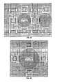
- FIGS. 4A and 4Bshow representative pixel layouts.
- FIG. 4Ashows a 6 by 6 square micron pixel layout while FIG. 4B shows an 81 ⁇ 2 by 81 ⁇ 2 micron pixel layout. In both Figures, four outputs are shown.
- FIG. 5shows a cross sectional potential diagram of an exemplary pinned photodiode.
- the generator carrierhas a time of flight within this limit. This resolution time constrains the size of the detector.
- the characteristic diffusion time in a semiconductor deviceis L 2 /D, where D is the diffusion coefficient. This time originates from the continuity equation and the diffusion equation, and defines how soon the steady state will be established in the area of size L. Hence, for a 10 cm square per second electron diffusion coefficient, the characteristic size of the pinned photodiode could be less than 5 microns.
Landscapes
- Engineering & Computer Science (AREA)
- Computer Networks & Wireless Communication (AREA)
- Physics & Mathematics (AREA)
- General Physics & Mathematics (AREA)
- Radar, Positioning & Navigation (AREA)
- Remote Sensing (AREA)
- Solid State Image Pick-Up Elements (AREA)
- Transforming Light Signals Into Electric Signals (AREA)
- Photometry And Measurement Of Optical Pulse Characteristics (AREA)
Abstract
Description
Claims (25)
Priority Applications (5)
| Application Number | Priority Date | Filing Date | Title |
|---|---|---|---|
| US09/867,846US6794214B2 (en) | 1998-08-19 | 2001-05-29 | Lock in pinned photodiode photodetector |
| US10/459,595US6750485B2 (en) | 1998-08-19 | 2003-06-12 | Lock in pinned photodiode photodetector |
| US11/524,495USRE41340E1 (en) | 1998-08-19 | 2006-09-21 | Pinned photodiode photodetector with common buffer transistor and binning capability |
| US12/413,626USRE42292E1 (en) | 1998-08-19 | 2009-03-30 | Pinned photodiode photodetector with common pixel transistors and binning capability |
| US13/343,843USRE44482E1 (en) | 1998-08-19 | 2012-01-05 | CMOS active image sensor with common pixel transistors and binning capability |
Applications Claiming Priority (3)
| Application Number | Priority Date | Filing Date | Title |
|---|---|---|---|
| US9713598P | 1998-08-19 | 1998-08-19 | |
| US09/378,565US6239456B1 (en) | 1998-08-19 | 1999-08-19 | Lock in pinned photodiode photodetector |
| US09/867,846US6794214B2 (en) | 1998-08-19 | 2001-05-29 | Lock in pinned photodiode photodetector |
Related Parent Applications (3)
| Application Number | Title | Priority Date | Filing Date |
|---|---|---|---|
| US09/378,565ContinuationUS6239456B1 (en) | 1998-08-19 | 1999-08-19 | Lock in pinned photodiode photodetector |
| US11/524,495DivisionUSRE41340E1 (en) | 1998-08-19 | 2006-09-21 | Pinned photodiode photodetector with common buffer transistor and binning capability |
| US201113009268AContinuation | 1998-08-19 | 2011-01-19 |
Related Child Applications (4)
| Application Number | Title | Priority Date | Filing Date |
|---|---|---|---|
| US10/459,595DivisionUS6750485B2 (en) | 1998-08-19 | 2003-06-12 | Lock in pinned photodiode photodetector |
| US11/524,495ReissueUSRE41340E1 (en) | 1998-08-19 | 2006-09-21 | Pinned photodiode photodetector with common buffer transistor and binning capability |
| US12/413,626ReissueUSRE42292E1 (en) | 1998-08-19 | 2009-03-30 | Pinned photodiode photodetector with common pixel transistors and binning capability |
| US13/343,843ReissueUSRE44482E1 (en) | 1998-08-19 | 2012-01-05 | CMOS active image sensor with common pixel transistors and binning capability |
Publications (2)
| Publication Number | Publication Date |
|---|---|
| US20010052605A1 US20010052605A1 (en) | 2001-12-20 |
| US6794214B2true US6794214B2 (en) | 2004-09-21 |
Family
ID=44509844
Family Applications (6)
| Application Number | Title | Priority Date | Filing Date |
|---|---|---|---|
| US09/378,565Expired - LifetimeUS6239456B1 (en) | 1998-08-19 | 1999-08-19 | Lock in pinned photodiode photodetector |
| US09/867,846CeasedUS6794214B2 (en) | 1998-08-19 | 2001-05-29 | Lock in pinned photodiode photodetector |
| US10/459,595Expired - LifetimeUS6750485B2 (en) | 1998-08-19 | 2003-06-12 | Lock in pinned photodiode photodetector |
| US11/524,495Expired - LifetimeUSRE41340E1 (en) | 1998-08-19 | 2006-09-21 | Pinned photodiode photodetector with common buffer transistor and binning capability |
| US12/413,626Expired - LifetimeUSRE42292E1 (en) | 1998-08-19 | 2009-03-30 | Pinned photodiode photodetector with common pixel transistors and binning capability |
| US13/343,843Expired - LifetimeUSRE44482E1 (en) | 1998-08-19 | 2012-01-05 | CMOS active image sensor with common pixel transistors and binning capability |
Family Applications Before (1)
| Application Number | Title | Priority Date | Filing Date |
|---|---|---|---|
| US09/378,565Expired - LifetimeUS6239456B1 (en) | 1998-08-19 | 1999-08-19 | Lock in pinned photodiode photodetector |
Family Applications After (4)
| Application Number | Title | Priority Date | Filing Date |
|---|---|---|---|
| US10/459,595Expired - LifetimeUS6750485B2 (en) | 1998-08-19 | 2003-06-12 | Lock in pinned photodiode photodetector |
| US11/524,495Expired - LifetimeUSRE41340E1 (en) | 1998-08-19 | 2006-09-21 | Pinned photodiode photodetector with common buffer transistor and binning capability |
| US12/413,626Expired - LifetimeUSRE42292E1 (en) | 1998-08-19 | 2009-03-30 | Pinned photodiode photodetector with common pixel transistors and binning capability |
| US13/343,843Expired - LifetimeUSRE44482E1 (en) | 1998-08-19 | 2012-01-05 | CMOS active image sensor with common pixel transistors and binning capability |
Country Status (1)
| Country | Link |
|---|---|
| US (6) | US6239456B1 (en) |
Cited By (9)
| Publication number | Priority date | Publication date | Assignee | Title |
|---|---|---|---|---|
| US20030223053A1 (en)* | 2000-12-11 | 2003-12-04 | Xingiao Liu | Methods and devices for charge management for three-dimensional and color sensing |
| US20060192938A1 (en)* | 2003-02-03 | 2006-08-31 | National University Corporation Shizuoka University | Distance image sensor |
| US20080225144A1 (en)* | 2007-03-12 | 2008-09-18 | Micron Technology, Inc. | Multi-purpose image sensor circuits, imager, system and method of operation |
| US20090059989A1 (en)* | 2007-08-31 | 2009-03-05 | Em Microelectronic-Marin S.A. | Optoelectronic circuit with a photoreceptor and a laser diode, and module comprising the same |
| US20090224139A1 (en)* | 2008-03-04 | 2009-09-10 | Mesa Imaging Ag | Drift Field Demodulation Pixel with Pinned Photo Diode |
| US20100308209A1 (en)* | 2009-06-09 | 2010-12-09 | Mesa Imaging Ag | System for Charge-Domain Electron Subtraction in Demodulation Pixels and Method Therefor |
| US9117712B1 (en) | 2009-07-24 | 2015-08-25 | Mesa Imaging Ag | Demodulation pixel with backside illumination and charge barrier |
| US9410800B1 (en) | 2010-08-02 | 2016-08-09 | Heptagon Micro Optics Pte. Ltd. | 3D TOF camera with masked illumination |
| KR20170134550A (en) | 2015-03-31 | 2017-12-06 | 고쿠리츠 다이가꾸 호우진 시즈오까 다이가꾸 | And a solid-state imaging device |
Families Citing this family (30)
| Publication number | Priority date | Publication date | Assignee | Title |
|---|---|---|---|---|
| US7199410B2 (en)* | 1999-12-14 | 2007-04-03 | Cypress Semiconductor Corporation (Belgium) Bvba | Pixel structure with improved charge transfer |
| US6239456B1 (en) | 1998-08-19 | 2001-05-29 | Photobit Corporation | Lock in pinned photodiode photodetector |
| US20020063198A1 (en)* | 2000-10-26 | 2002-05-30 | Krymski Alexander I. | Frame shutter for CMOS APS |
| US6987240B2 (en)* | 2002-04-18 | 2006-01-17 | Applied Materials, Inc. | Thermal flux processing by scanning |
| US7489352B2 (en)* | 2002-11-15 | 2009-02-10 | Micron Technology, Inc. | Wide dynamic range pinned photodiode active pixel sensor (APS) |
| US7808022B1 (en) | 2005-03-28 | 2010-10-05 | Cypress Semiconductor Corporation | Cross talk reduction |
| US7750958B1 (en) | 2005-03-28 | 2010-07-06 | Cypress Semiconductor Corporation | Pixel structure |
| US7671460B2 (en)* | 2006-01-25 | 2010-03-02 | Teledyne Licensing, Llc | Buried via technology for three dimensional integrated circuits |
| US7947941B2 (en)* | 2006-11-01 | 2011-05-24 | Finisar Corporation | Photodiode having rounded edges for high electrostatic discharge threshold |
| US7923763B2 (en)* | 2007-03-08 | 2011-04-12 | Teledyne Licensing, Llc | Two-dimensional time delay integration visible CMOS image sensor |
| US20090166684A1 (en)* | 2007-12-26 | 2009-07-02 | 3Dv Systems Ltd. | Photogate cmos pixel for 3d cameras having reduced intra-pixel cross talk |
| EP2296368B1 (en)* | 2008-06-04 | 2017-01-04 | Shizuoka University | Imaging device |
| JP5501358B2 (en)* | 2008-07-17 | 2014-05-21 | マイクロソフト インターナショナル ホールディングス ビイ.ヴイ. | CMOS photogate 3D camera system with improved charge sensing cell and pixel geometry |
| US7795650B2 (en)* | 2008-12-09 | 2010-09-14 | Teledyne Scientific & Imaging Llc | Method and apparatus for backside illuminated image sensors using capacitively coupled readout integrated circuits |
| US8785831B2 (en) | 2011-01-05 | 2014-07-22 | Luxima Technology LLC | Image sensors and methods with high speed global shutter pixels |
| EP2708021B1 (en) | 2011-05-12 | 2019-07-10 | DePuy Synthes Products, Inc. | Image sensor with tolerance optimizing interconnects |
| JP6041500B2 (en)* | 2012-03-01 | 2016-12-07 | キヤノン株式会社 | Imaging device, imaging system, driving method of imaging device, and driving method of imaging system |
| MX346174B (en) | 2012-07-26 | 2017-03-10 | Depuy Synthes Products Inc | YCBCR PULSED LIGHTING SCHEME IN A DEFICIENT LIGHT ENVIRONMENT. |
| US9462234B2 (en) | 2012-07-26 | 2016-10-04 | DePuy Synthes Products, Inc. | Camera system with minimal area monolithic CMOS image sensor |
| MX389501B (en) | 2012-07-26 | 2025-03-20 | Depuy Synthes Products Inc | CONTINUOUS VIDEO IN A LIGHT-POOR ENVIRONMENT |
| AU2014223163A1 (en) | 2013-02-28 | 2015-08-20 | Olive Medical Corporation | Videostroboscopy of vocal chords with CMOS sensors |
| US8908063B2 (en)* | 2013-03-11 | 2014-12-09 | Texas Instruments Incorporated | Method and apparatus for a time-of-flight sensor with charge storage |
| CA2906821A1 (en) | 2013-03-15 | 2014-09-18 | Olive Medical Corporation | Scope sensing in a light controlled environment |
| CA2906975A1 (en) | 2013-03-15 | 2014-09-18 | Olive Medical Corporation | Minimize image sensor i/o and conductor counts in endoscope applications |
| EP2967285B1 (en) | 2013-03-15 | 2023-08-16 | DePuy Synthes Products, Inc. | Image sensor synchronization without input clock and data transmission clock |
| WO2014145249A1 (en) | 2013-03-15 | 2014-09-18 | Olive Medical Corporation | Controlling the integral light energy of a laser pulse |
| WO2014144947A1 (en) | 2013-03-15 | 2014-09-18 | Olive Medical Corporation | Super resolution and color motion artifact correction in a pulsed color imaging system |
| US9369648B2 (en) | 2013-06-18 | 2016-06-14 | Alexander Krymski | Image sensors, methods, and pixels with tri-level biased transfer gates |
| US9762890B2 (en) | 2013-11-08 | 2017-09-12 | Samsung Electronics Co., Ltd. | Distance sensor and image processing system including the same |
| WO2015143453A1 (en) | 2014-03-21 | 2015-09-24 | Olive Medical Corporation | Card edge connector for an imaging sensor |
Citations (7)
| Publication number | Priority date | Publication date | Assignee | Title |
|---|---|---|---|---|
| US5043568A (en)* | 1989-04-11 | 1991-08-27 | Hamamatsu Photonics K. K. | Optical signal detector incorporating means for eluminating background light |
| US5099694A (en)* | 1987-05-19 | 1992-03-31 | Canon Kabushiki Kaisha | Vibration detecting apparatus |
| US5179565A (en)* | 1990-06-07 | 1993-01-12 | Hamamatsu Photonics, K.K. | Low noise pulsed light source utilizing laser diode and voltage detector device utilizing same low noise pulsed light source |
| US5497390A (en)* | 1992-01-31 | 1996-03-05 | Nippon Telegraph And Telephone Corporation | Polarization mode switching semiconductor laser apparatus |
| US5880495A (en)* | 1998-01-08 | 1999-03-09 | Omnivision Technologies, Inc. | Active pixel with a pinned photodiode |
| US6100551A (en)* | 1995-04-13 | 2000-08-08 | Eastman Kodak Company | Active pixel sensor integrated with a pinned photodiode |
| US6127697A (en)* | 1997-11-14 | 2000-10-03 | Eastman Kodak Company | CMOS image sensor |
Family Cites Families (50)
| Publication number | Priority date | Publication date | Assignee | Title |
|---|---|---|---|---|
| DE3525395A1 (en) | 1984-07-17 | 1986-01-30 | Canon K.K., Tokio/Tokyo | IMAGE READER |
| JPS63100879A (en) | 1986-10-17 | 1988-05-02 | Hitachi Ltd | solid-state imaging device |
| DE69033613T2 (en) | 1989-05-31 | 2001-05-03 | Canon K.K., Tokio/Tokyo | Photoelectric converter |
| US5262871A (en) | 1989-11-13 | 1993-11-16 | Rutgers, The State University | Multiple resolution image sensor |
| JP2915482B2 (en) | 1990-04-23 | 1999-07-05 | キヤノン株式会社 | Photoelectric conversion device |
| JP2915483B2 (en) | 1990-04-23 | 1999-07-05 | キヤノン株式会社 | Photoelectric conversion device |
| US5148268A (en)* | 1991-04-26 | 1992-09-15 | Xerox Corporation | Multiplexing arrangement for controlling data produced by a color images sensor array |
| JP2977060B2 (en) | 1992-01-29 | 1999-11-10 | オリンパス光学工業株式会社 | Solid-state imaging device and control method thereof |
| DE69418754T2 (en) | 1993-03-15 | 1999-11-04 | Canon K.K., Tokio/Tokyo | Signal processor |
| US5471505A (en)* | 1993-10-01 | 1995-11-28 | Elsag International N.V. | Method and apparatus for increasing the resolution of a digital to analog converted pulse width modulated signal |
| US5949483A (en) | 1994-01-28 | 1999-09-07 | California Institute Of Technology | Active pixel sensor array with multiresolution readout |
| CA2156530A1 (en) | 1994-10-11 | 1996-04-12 | Alexander George Dickinson | Active pixel image sensor |
| US5739562A (en) | 1995-08-01 | 1998-04-14 | Lucent Technologies Inc. | Combined photogate and photodiode active pixel image sensor |
| JP3031606B2 (en) | 1995-08-02 | 2000-04-10 | キヤノン株式会社 | Solid-state imaging device and image imaging device |
| US5635705A (en) | 1995-09-11 | 1997-06-03 | Irvine Sensors Corporation | Sensing and selecting observed events for signal processing |
| US5717199A (en) | 1996-01-26 | 1998-02-10 | Cid Technologies, Inc. | Collective charge reading and injection in random access charge transfer devices |
| US5790191A (en) | 1996-03-07 | 1998-08-04 | Omnivision Technologies, Inc. | Method and apparatus for preamplification in a MOS imaging array |
| US5781233A (en)* | 1996-03-14 | 1998-07-14 | Tritech Microelectronics, Ltd. | MOS FET camera chip and methods of manufacture and operation thereof |
| US6750527B1 (en) | 1996-05-30 | 2004-06-15 | Kabushiki Kaisha Toshiba | Semiconductor integrated circuit device having a plurality of wells, test method of testing the semiconductor integrated circuit device, and test device which executes the test method |
| US5936986A (en)* | 1996-07-30 | 1999-08-10 | Bayer Corporation | Methods and apparatus for driving a laser diode |
| US5691486A (en)* | 1996-07-30 | 1997-11-25 | Bayer Corporation | Apparatus and methods for selecting a variable number of test sample aliquots to mix with respective reagents |
| US5970115A (en) | 1996-11-29 | 1999-10-19 | Varian Medical Systems, Inc. | Multiple mode digital X-ray imaging system |
| US6297070B1 (en) | 1996-12-20 | 2001-10-02 | Eastman Kodak Company | Active pixel sensor integrated with a pinned photodiode |
| US5973311A (en) | 1997-02-12 | 1999-10-26 | Imation Corp | Pixel array with high and low resolution mode |
| US6160281A (en) | 1997-02-28 | 2000-12-12 | Eastman Kodak Company | Active pixel sensor with inter-pixel function sharing |
| US5898168A (en) | 1997-06-12 | 1999-04-27 | International Business Machines Corporation | Image sensor pixel circuit |
| US6107655A (en) | 1997-08-15 | 2000-08-22 | Eastman Kodak Company | Active pixel image sensor with shared amplifier read-out |
| JP3620237B2 (en)* | 1997-09-29 | 2005-02-16 | ソニー株式会社 | Solid-state image sensor |
| US6233013B1 (en)* | 1997-10-23 | 2001-05-15 | Xerox Corporation | Color readout system for an active pixel image sensor |
| US6714239B2 (en)* | 1997-10-29 | 2004-03-30 | Eastman Kodak Company | Active pixel sensor with programmable color balance |
| ATE202882T1 (en) | 1997-12-18 | 2001-07-15 | Simage Oy | DEVICE FOR RADIATION IMAGE RECORDING |
| US5986510A (en) | 1998-01-09 | 1999-11-16 | Reticon Corporation | Method and apparatus for amplifying input signals in one of multiple modes of resolution |
| US6377304B1 (en) | 1998-02-05 | 2002-04-23 | Nikon Corporation | Solid-state image-pickup devices exhibiting faster video-frame processing rates, and associated methods |
| US6667768B1 (en)* | 1998-02-17 | 2003-12-23 | Micron Technology, Inc. | Photodiode-type pixel for global electronic shutter and reduced lag |
| US6084229A (en) | 1998-03-16 | 2000-07-04 | Photon Vision Systems, Llc | Complimentary metal oxide semiconductor imaging device |
| US6977684B1 (en) | 1998-04-30 | 2005-12-20 | Canon Kabushiki Kaisha | Arrangement of circuits in pixels, each circuit shared by a plurality of pixels, in image sensing apparatus |
| KR19990084630A (en) | 1998-05-08 | 1999-12-06 | 김영환 | CMOS image sensor and its driving method |
| US6043478A (en)* | 1998-06-25 | 2000-03-28 | Industrial Technology Research Institute | Active pixel sensor with shared readout structure |
| GB2339333B (en)* | 1998-06-29 | 2003-07-09 | Hyundai Electronics Ind | Photodiode having charge function and image sensor using the same |
| US6512546B1 (en) | 1998-07-17 | 2003-01-28 | Analog Devices, Inc. | Image sensor using multiple array readout lines |
| US6239456B1 (en)* | 1998-08-19 | 2001-05-29 | Photobit Corporation | Lock in pinned photodiode photodetector |
| JP2000152086A (en) | 1998-11-11 | 2000-05-30 | Canon Inc | Imaging device and imaging system |
| US6249618B1 (en) | 1998-12-18 | 2001-06-19 | Syscan, Inc. | Circuit architecture and method for switching sensor resolution |
| US6657665B1 (en) | 1998-12-31 | 2003-12-02 | Eastman Kodak Company | Active Pixel Sensor with wired floating diffusions and shared amplifier |
| WO2000052765A1 (en)* | 1999-03-01 | 2000-09-08 | Photobit Corporation | Active pixel sensor with fully-depleted buried photoreceptor |
| US6693670B1 (en) | 1999-07-29 | 2004-02-17 | Vision - Sciences, Inc. | Multi-photodetector unit cell |
| AU1190501A (en) | 1999-09-30 | 2001-04-30 | California Institute Of Technology | High-speed on-chip windowed centroiding using photodiode-based cmos imager |
| US6831690B1 (en) | 1999-12-07 | 2004-12-14 | Symagery Microsystems, Inc. | Electrical sensing apparatus and method utilizing an array of transducer elements |
| JP4721380B2 (en) | 2000-04-14 | 2011-07-13 | キヤノン株式会社 | Solid-state imaging device and imaging system |
| US7859581B2 (en) | 2003-07-15 | 2010-12-28 | Eastman Kodak Company | Image sensor with charge binning and dual channel readout |
- 1999
- 1999-08-19USUS09/378,565patent/US6239456B1/ennot_activeExpired - Lifetime
- 2001
- 2001-05-29USUS09/867,846patent/US6794214B2/ennot_activeCeased
- 2003
- 2003-06-12USUS10/459,595patent/US6750485B2/ennot_activeExpired - Lifetime
- 2006
- 2006-09-21USUS11/524,495patent/USRE41340E1/ennot_activeExpired - Lifetime
- 2009
- 2009-03-30USUS12/413,626patent/USRE42292E1/ennot_activeExpired - Lifetime
- 2012
- 2012-01-05USUS13/343,843patent/USRE44482E1/ennot_activeExpired - Lifetime
Patent Citations (7)
| Publication number | Priority date | Publication date | Assignee | Title |
|---|---|---|---|---|
| US5099694A (en)* | 1987-05-19 | 1992-03-31 | Canon Kabushiki Kaisha | Vibration detecting apparatus |
| US5043568A (en)* | 1989-04-11 | 1991-08-27 | Hamamatsu Photonics K. K. | Optical signal detector incorporating means for eluminating background light |
| US5179565A (en)* | 1990-06-07 | 1993-01-12 | Hamamatsu Photonics, K.K. | Low noise pulsed light source utilizing laser diode and voltage detector device utilizing same low noise pulsed light source |
| US5497390A (en)* | 1992-01-31 | 1996-03-05 | Nippon Telegraph And Telephone Corporation | Polarization mode switching semiconductor laser apparatus |
| US6100551A (en)* | 1995-04-13 | 2000-08-08 | Eastman Kodak Company | Active pixel sensor integrated with a pinned photodiode |
| US6127697A (en)* | 1997-11-14 | 2000-10-03 | Eastman Kodak Company | CMOS image sensor |
| US5880495A (en)* | 1998-01-08 | 1999-03-09 | Omnivision Technologies, Inc. | Active pixel with a pinned photodiode |
Cited By (17)
| Publication number | Priority date | Publication date | Assignee | Title |
|---|---|---|---|---|
| US20050156121A1 (en)* | 2000-11-09 | 2005-07-21 | Canesta, Inc. | Methods and devices for charge management for three-dimensional and color sensing |
| US7464351B2 (en) | 2000-11-09 | 2008-12-09 | Canesta, Inc. | Method enabling a standard CMOS fab to produce an IC to sense three-dimensional information using augmented rules creating mask patterns not otherwise expressible with existing fab rules |
| US6906793B2 (en) | 2000-12-11 | 2005-06-14 | Canesta, Inc. | Methods and devices for charge management for three-dimensional sensing |
| US20030223053A1 (en)* | 2000-12-11 | 2003-12-04 | Xingiao Liu | Methods and devices for charge management for three-dimensional and color sensing |
| US20060192938A1 (en)* | 2003-02-03 | 2006-08-31 | National University Corporation Shizuoka University | Distance image sensor |
| US7436496B2 (en) | 2003-02-03 | 2008-10-14 | National University Corporation Shizuoka University | Distance image sensor |
| US7724293B2 (en) | 2007-03-12 | 2010-05-25 | Aptina Imaging Corporation | Multi-purpose image sensor circuits, imager, system and method of operation |
| US20080225144A1 (en)* | 2007-03-12 | 2008-09-18 | Micron Technology, Inc. | Multi-purpose image sensor circuits, imager, system and method of operation |
| US7957448B2 (en)* | 2007-08-31 | 2011-06-07 | Em Microelectronic-Marin S.A. | Optoelectronic circuit with a photoreceptor and a laser diode, and module comprising the same |
| US20090059989A1 (en)* | 2007-08-31 | 2009-03-05 | Em Microelectronic-Marin S.A. | Optoelectronic circuit with a photoreceptor and a laser diode, and module comprising the same |
| US20090224139A1 (en)* | 2008-03-04 | 2009-09-10 | Mesa Imaging Ag | Drift Field Demodulation Pixel with Pinned Photo Diode |
| US20100308209A1 (en)* | 2009-06-09 | 2010-12-09 | Mesa Imaging Ag | System for Charge-Domain Electron Subtraction in Demodulation Pixels and Method Therefor |
| WO2010144616A1 (en) | 2009-06-09 | 2010-12-16 | Mesa Imaging Ag | System for charge-domain electron subtraction in demodulation pixels and method therefor |
| US9117712B1 (en) | 2009-07-24 | 2015-08-25 | Mesa Imaging Ag | Demodulation pixel with backside illumination and charge barrier |
| US9410800B1 (en) | 2010-08-02 | 2016-08-09 | Heptagon Micro Optics Pte. Ltd. | 3D TOF camera with masked illumination |
| KR20170134550A (en) | 2015-03-31 | 2017-12-06 | 고쿠리츠 다이가꾸 호우진 시즈오까 다이가꾸 | And a solid-state imaging device |
| US10325953B2 (en) | 2015-03-31 | 2019-06-18 | National University Corporation Shizuoka University | Range sensor and solid-state imaging device |
Also Published As
| Publication number | Publication date |
|---|---|
| USRE44482E1 (en) | 2013-09-10 |
| US20010052605A1 (en) | 2001-12-20 |
| US6239456B1 (en) | 2001-05-29 |
| US20030213984A1 (en) | 2003-11-20 |
| USRE42292E1 (en) | 2011-04-12 |
| US6750485B2 (en) | 2004-06-15 |
| USRE41340E1 (en) | 2010-05-18 |
Similar Documents
| Publication | Publication Date | Title |
|---|---|---|
| US6794214B2 (en) | Lock in pinned photodiode photodetector | |
| US8760549B2 (en) | Demodulation pixel with daisy chain charge storage sites and method of operation therefor | |
| KR100675765B1 (en) | Spatial information detection device using intensity modulated light | |
| Lange et al. | Demodulation pixels in CCD and CMOS technologies for time-of-flight ranging | |
| US7622704B2 (en) | Optoelectronic detector with multiple readout nodes and its use thereof | |
| US8115158B2 (en) | Device and method for the demodulation of modulated electromagnetic wave fields | |
| US20090224139A1 (en) | Drift Field Demodulation Pixel with Pinned Photo Diode | |
| EP1152261A1 (en) | Device and method for spatially resolved photodetection and demodulation of modulated electromagnetic waves | |
| US8829408B2 (en) | Sensor pixel array and separated array of storage and accumulation with parallel acquisition and readout wherein each pixel includes storage sites and readout nodes | |
| JP2002516490A (en) | Apparatus and method for detecting phase and amplitude of electromagnetic wave | |
| Burke et al. | Charge-injection imaging: Operating techniques and performances characteristics | |
| US6498346B1 (en) | Large dynamic range focal plane array | |
| Hong | On-chip spatial image processing with CMOS active pixel sensors | |
| US7269359B1 (en) | Focal plane array with synchronous detection circuits for an active remote sensing system | |
| JP3643210B2 (en) | Time correlation detection type image sensor and image analysis method | |
| Weimer et al. | Self-scanned image sensors based on charge transfer by the bucket-brigade method | |
| Pancheri et al. | Sensors based on in-pixel photo-mixing devices | |
| US20220113425A1 (en) | Device of acquisition of a 2d image and of a depth image of a scene | |
| EP0066020B1 (en) | Infrared energy detector system utilizing a charge transfer device sensor | |
| CN115835037A (en) | Single-path photoelectric semiconductor element, photoelectric modulator and electronic equipment | |
| Loeliger et al. | Sweep photogate: optimized photosensors for optical spectrometry in CMOS | |
| Weckler et al. | Design possibilities for photodiode arrays with integral silicon-gate scan generators |
Legal Events
| Date | Code | Title | Description |
|---|---|---|---|
| AS | Assignment | Owner name:MICRON TECHNOLOGY, INC., IDAHO Free format text:ASSIGNMENT OF ASSIGNORS INTEREST;ASSIGNOR:PHOTOBIT CORPORATION;REEL/FRAME:012745/0385 Effective date:20011121 Owner name:MICRON TECHNOLOGY, INC., IDAHO Free format text:ASSIGNMENT OF ASSIGNORS INTEREST;ASSIGNOR:PHOTOBIT CORPORATION;REEL/FRAME:014007/0590 Effective date:20011121 | |
| STCF | Information on status: patent grant | Free format text:PATENTED CASE | |
| CC | Certificate of correction | ||
| RF | Reissue application filed | Effective date:20060921 | |
| FEPP | Fee payment procedure | Free format text:PAT HOLDER NO LONGER CLAIMS SMALL ENTITY STATUS, ENTITY STATUS SET TO UNDISCOUNTED (ORIGINAL EVENT CODE: STOL); ENTITY STATUS OF PATENT OWNER: LARGE ENTITY Free format text:PAYOR NUMBER ASSIGNED (ORIGINAL EVENT CODE: ASPN); ENTITY STATUS OF PATENT OWNER: LARGE ENTITY | |
| REFU | Refund | Free format text:REFUND - SURCHARGE, PETITION TO ACCEPT PYMT AFTER EXP, UNINTENTIONAL (ORIGINAL EVENT CODE: R2551); ENTITY STATUS OF PATENT OWNER: LARGE ENTITY | |
| FPAY | Fee payment | Year of fee payment:4 | |
| RF | Reissue application filed | Effective date:20090330 | |
| AS | Assignment | Owner name:ROUND ROCK RESEARCH, LLC,NEW YORK Free format text:ASSIGNMENT OF ASSIGNORS INTEREST;ASSIGNOR:MICRON TECHNOLOGY, INC.;REEL/FRAME:023786/0416 Effective date:20091223 Owner name:ROUND ROCK RESEARCH, LLC, NEW YORK Free format text:ASSIGNMENT OF ASSIGNORS INTEREST;ASSIGNOR:MICRON TECHNOLOGY, INC.;REEL/FRAME:023786/0416 Effective date:20091223 | |
| RF | Reissue application filed | Effective date:20110119 |