US6791735B2 - Differentially-driven MEMS spatial light modulator - Google Patents
Differentially-driven MEMS spatial light modulatorDownload PDFInfo
- Publication number
- US6791735B2 US6791735B2US10/340,317US34031703AUS6791735B2US 6791735 B2US6791735 B2US 6791735B2US 34031703 AUS34031703 AUS 34031703AUS 6791735 B2US6791735 B2US 6791735B2
- Authority
- US
- United States
- Prior art keywords
- center electrode
- voltage
- center
- electrode
- electrodes
- Prior art date
- Legal status (The legal status is an assumption and is not a legal conclusion. Google has not performed a legal analysis and makes no representation as to the accuracy of the status listed.)
- Expired - Fee Related
Links
- 230000004044responseEffects0.000claimsdescription13
- 238000006073displacement reactionMethods0.000claimsdescription12
- 238000000034methodMethods0.000claimsdescription6
- 230000008569processEffects0.000claimsdescription4
- 239000010410layerSubstances0.000description16
- 238000013461designMethods0.000description7
- 230000001965increasing effectEffects0.000description6
- 239000000463materialSubstances0.000description4
- 239000000758substrateSubstances0.000description4
- 230000003044adaptive effectEffects0.000description3
- 230000009467reductionEffects0.000description3
- 230000008901benefitEffects0.000description2
- 238000012937correctionMethods0.000description2
- 230000007423decreaseEffects0.000description2
- 235000001674Agaricus brunnescensNutrition0.000description1
- 101100121123Caenorhabditis elegans gap-1 geneProteins0.000description1
- 101100282111Caenorhabditis elegans gap-2 geneProteins0.000description1
- VYPSYNLAJGMNEJ-UHFFFAOYSA-NSilicium dioxideChemical compoundO=[Si]=OVYPSYNLAJGMNEJ-UHFFFAOYSA-N0.000description1
- 230000008859changeEffects0.000description1
- 239000011248coating agentSubstances0.000description1
- 238000000576coating methodMethods0.000description1
- 238000004891communicationMethods0.000description1
- 238000010276constructionMethods0.000description1
- 238000001816coolingMethods0.000description1
- 230000003247decreasing effectEffects0.000description1
- 230000007123defenseEffects0.000description1
- 230000001419dependent effectEffects0.000description1
- 230000000694effectsEffects0.000description1
- 230000005684electric fieldEffects0.000description1
- 239000012777electrically insulating materialSubstances0.000description1
- 238000004146energy storageMethods0.000description1
- 238000005516engineering processMethods0.000description1
- 230000002708enhancing effectEffects0.000description1
- 239000005350fused silica glassSubstances0.000description1
- 238000003384imaging methodMethods0.000description1
- 230000010354integrationEffects0.000description1
- 238000012986modificationMethods0.000description1
- 230000004048modificationEffects0.000description1
- 230000003287optical effectEffects0.000description1
- 238000005381potential energyMethods0.000description1
- 230000035484reaction timeEffects0.000description1
- 238000011160researchMethods0.000description1
- 239000002356single layerSubstances0.000description1
- 230000002269spontaneous effectEffects0.000description1
Images


Classifications
- G—PHYSICS
- G02—OPTICS
- G02B—OPTICAL ELEMENTS, SYSTEMS OR APPARATUS
- G02B26/00—Optical devices or arrangements for the control of light using movable or deformable optical elements
- G02B26/08—Optical devices or arrangements for the control of light using movable or deformable optical elements for controlling the direction of light
- G02B26/0816—Optical devices or arrangements for the control of light using movable or deformable optical elements for controlling the direction of light by means of one or more reflecting elements
- G02B26/0833—Optical devices or arrangements for the control of light using movable or deformable optical elements for controlling the direction of light by means of one or more reflecting elements the reflecting element being a micromechanical device, e.g. a MEMS mirror, DMD
- G02B26/0841—Optical devices or arrangements for the control of light using movable or deformable optical elements for controlling the direction of light by means of one or more reflecting elements the reflecting element being a micromechanical device, e.g. a MEMS mirror, DMD the reflecting element being moved or deformed by electrostatic means
Definitions
- the present inventionrelates to spatial light modulators.
- the inventionrelates more particularly to low voltage MEMS-based (micromachined electromechanical system) electrostatic actuators and MEMS-based phase spatial light modulators utilizing the same.
- SLMsspatial light modulators
- AOadaptive optics
- MEMS AO designshave typically been based on conventional parallel plate electrostatic actuators as shown in FIG. 1, and generally indicated at reference character 100 .
- the actuator 100is shown having two parallel plates 101 and 102 which are spaced apart with an electric voltage 104 applied therebetween. While not shown, the lower plate 101 is typically fixed, while the upper plate 102 is movable in a direction normal to the surface of the plate. Additionally, the conventional parallel plate electrostatic actuator is modeled to account for mechanical energy storage, such as potential energy storage in a flexible plate or a spring connected to a rigid plate (see 105 ), or the kinetic energy generated by plate movement. As shown in FIG. 1, the movable plate 102 is typically a mirror having a reflective surface 103 to reflect incident light 106 , as indicated by arrow 107 . As an alternative (not shown) a mirror is often connected to the movable plate by means of a connecting anchor, in order to prevent mirror warpage due to plate movement.
- High voltage transistorsare much larger than low voltage transistors used in common integrated circuits, making it challenging to integrate the required circuitry. Moreover, the large space requirements of high voltage transistors leave little or no room for other control electronics, such as feedback control circuits. And high voltage power supplies typically dominate the overall system size. The power dissipation from high voltage drivers is also a concern, as temperature gradients may cause mirror warpage. And with high voltage drivers, active cooling may be required which further increases system complexity, size, and cost.
- FIG. 2shows a graph illustrating the strongly non-linear displacement-versus-voltage characteristics typically seen in present SLM devices, (e.g. utilizing a conventional parallel plate electrostatic actuator).
- SLM devicestherefore require high precision electronics drivers for adaptive control and error correction, further increasing complexity, size, and cost.
- One aspect of the present inventionincludes an electrostatic actuator associated with a pixel in a spatial light modulator having a plurality of pixels.
- the actuatorcomprises: a lower electrode; an upper electrode fixed with respect to the lower electrode; a center electrode suspended and actuable between the upper and lower electrodes, and having resiliently-biasing means for restoring the center electrode to a non-actuated first equilibrium position; a mirror operably connected to the center electrode; a first voltage source for providing a first bias voltage across the lower and center electrodes; a second voltage source for providing a second bias voltage across the upper and center electrodes, wherein the first and second bias voltages determine the non-actuated first equilibrium position of the center electrode; and a third voltage source for providing a variable driver voltage across one of the lower/center and upper/center electrode pairs in series with the corresponding first or second bias voltage, for actuating the center electrode to a dynamic second equilibrium position.
- a spatial light modulatorcomprising: an array of electrostatic actuators, each representing a pixel of the SLM and comprising: a lower electrode; an upper electrode fixed with respect to the lower electrode; a center electrode suspended and actuable between the upper and lower electrodes, and having resiliently-biasing means for restoring the center electrode to a non-actuated first equilibrium position; a mirror operably connected to the center electrode; a first voltage source for providing a first bias voltage across the lower and center electrodes; a second voltage source for providing a second bias voltage across the upper and center electrodes, wherein the first and second bias voltages determine the non-actuated first equilibrium position of the center electrode; and a third voltage source for providing a variable driver voltage across one of the lower/center and upper/center electrode pairs in series with the corresponding first or second bias voltage, for actuating the center electrode to a dynamic second equilibrium position.
- SLMspatial light modulator
- a MEMS electrostatic actuatorcomprising: a first electrode layer; a second electrode layer fixed with respect to the first electrode layer; a center electrode layer suspended and actuable between the first and second electrode layers and having resiliently-biasing means for restoring the center electrode layer to a non-actuated first equilibrium position; a first voltage source for providing a first bias voltage across the first and center electrode layers; a second voltage source for providing a second bias voltage across the second and center electrode layers, wherein the first and second bias voltages determine the non-actuated first equilibrium position of the center electrode layer; and a third voltage source for providing a variable driver voltage across one of the first/center and second/center electrode layer pairs in series with the corresponding first or second bias voltage, for actuating the center electrode layer to a dynamic second equilibrium position.
- Another aspect of the present inventionincludes a process for controlling a spatial light modulator (SLM) comprising the steps of: providing a SLM having a plurality of electrostatic actuators, each actuator having a lower electrode, an upper electrode fixed with respect to the lower electrode, a center electrode suspended and actuable between the upper and lower electrodes with resiliently-biasing means for restoring the center electrode to a non-actuated first equilibrium position, and a mirror operably connected to the center electrode; for each electrostatic actuator, (a) providing a first bias voltage across the lower and center electrodes, and a second bias voltage across the upper and center electrodes, to establish the corresponding non-actuated first equilibrium position; and (b) applying a variable driver voltage across one of the lower/center and upper/center electrode pairs in series with the corresponding first or second bias voltage to actuate the center electrode to a dynamic second equilibrium position, wherein the variable driver voltage is applied independent of other actuators.
- SLMspatial light modulator
- Another aspect of the present inventionincludes an electrostatic actuation process comprising: providing first and second electrodes fixed relative to each other and a center electrode suspended and actuable between the first and second electrodes, the center electrode having resiliently-biasing means for restoring the center electrode to a non-actuated first equilibrium position; providing a first bias voltage across the first and center electrodes, and a second bias voltage across the second and center electrodes to establish the non-actuated first equilibrium position; and actuating the center electrode to a second dynamic equilibrium position by applying a variable driver voltage across one of the first/center and second/center electrode pairs in series with the corresponding first or second bias voltage.
- FIG. 1is a schematic elevational view of a conventional parallel plate electrostatic actuator known in the prior art.
- FIG. 2is a graph illustrating the nonlinearity of displacement response produced when a drive voltage is applied to a conventional parallel plate electrostatic actuator known in the prior art.
- FIG. 3is a schematic elevational view of a first exemplary embodiment of a MEMS electrostatic actuator of the present invention.
- FIG. 4is a schematic elevational view of a second exemplary embodiment of a MEMS electrostatic actuator of the present invention.
- FIG. 5is a schematic elevational view of a third exemplary embodiment of a single pixel electrostatic actuator of the present invention.
- FIG. 6is a schematic elevational and partial view of an exemplary phase SLM having a pixelized array of MEMS electrostatic actuators (two actuators shown).
- FIG. 7is a graph illustrating the substantial linearity of displacement response produce when a drive voltage is applied to the three-electrode actuator of the present invention.
- a MEMS-based electrostatic actuator and actuation methodsuch as those designed for use in SLMs, is disclosed having three electrodes: a lower electrode, an upper electrode fixed with respect to the lower electrode, and a center electrode suspended between the lower and upper electrodes.
- a bias voltageis applied between the lower and center electrodes (lower/center pair), and also between the upper and center electrodes (upper/center pair), though not necessarily of the same magnitude.
- the center electrodeis actuable between the lower and upper electrodes when a variable voltage is applied between one of the two electrode pairs.
- the driver voltageis preferably applied between the lower/center pair, primarily in order to allow positioning of driver electronics below and adjacent the lower electrode, as will be discussed herein. It is also notable that the fixed relationship between the upper and lower electrodes indicates that, at least during and for purposes of modulation, the distance between the upper electrode and lower electrode does not change.
- an SLM and an SLM control methodwhere the SLM has a plurality of pixels represented by an array of MEMS-based electrostatic actuators each having the three-electrode structure per pixel discussed above.
- the center electrodes of the pixelstogether form a pixelated actuator array (an electrode layer), which is held at a common electrical potential, e.g. ground.
- One of the upper electrode grouping (electrode layer) or lower electrode grouping (electrode layer)is preferably non-pixelated, i.e. having a single, undifferentiated-per-pixel, electrode construction across the SLM, and is held at a fixed bias voltage with respect to the center electrode(s).
- the other one of the upper electrode grouping or lower electrode grouping of the SLMis pixelated, with each pixelated electrode preferably having a bias voltage with respect to the center electrode.
- the lower electrode groupingis preferably selected as the pixelated electrode grouping for the same reason discussed above, i.e. to allow positioning of independent driver electronics below and adjacent each pixelated lower electrode.
- each of the pixelated and actuable center electrodesmay be actuated independent of other center electrodes. It is notable that the center electrodes are considered pixelated, not because of differentiated electric potentials therebetween, but because of their ability to be independently actuated relative to each other.
- the three-electrode arrangements of the present inventioneffectively reduce the variable driver or dynamic voltage required for actuation of the center movable electrode, and thereby also reduces the complexity, size and cost of the SLM electronics. It also effectively lowers power dissipation by reducing voltage, and simplifies the electronics by reducing the required voltage resolution (number of bits) due to a closer-to-linear phase vs. voltage characteristic compared to the prior art. It is notable that while voltage control is discussed herein, it is appreciated that charge control may be utilized in the alternative, though voltage control is generally easier to implement for small capacitances and is therefore the more common design in practical applications.
- FIG. 3shows a schematic elevational view of a first exemplary embodiment of a MEMS electrostatic actuator of the present invention, generally indicated at reference character 300 .
- the electrostatic actuatormay be representative of a single pixel in a multi-pixel electrostatic actuator array of an SLM.
- the electrostatic actuator 300has three electrodes (per pixel if as a part of a multi-electrode array of an SLM): a lower electrode 301 , a movable/actuable center electrode 302 , and an upper electrode 305 fixed with respect to the lower electrode.
- the three electrodesare shown each having a generally planar configuration and arranged generally parallel to each other.
- the movable center electrode 302is shown as a mirror having a reflective surface 303 on one side of the center electrode 302 for reflecting incident light as shown at 309 and 310 . It is appreciated, however, that the mirror and the center electrode may be structurally autonomous but still operably connected to each other, whereby movement of the center electrode likewise actuates the mirror. Additionally, the upper electrode is a transparent medium to the incident (laser) light 309 . Transparency may differ for different materials, with material selection dependent on the type and nature of the application. For example, Si is transparent in IR, and fused silica plus ITO coating in visible light.
- Actuation, and thus operation, of the three-electrode actuatoroccurs by controlling the voltages across the upper/center electrode pair and/or the lower/center electrode pair, to produce a net actuating force on the movable center electrode 302 .
- a bias voltage source 307is initially provided to produce a bias voltage V B2 across the upper/center electrode pair.
- a second bias voltage source 306is also provided to initially produce a bias voltage V B1 across the lower/center electrode pair.
- the center electrode 302is the electrical ground. Typical bias voltage ranges may be from about 10V to about 100V. Actual voltage selection may depend on the wavelength of the incident light to be modulated, since the required maximum deflection typically increases proportionally with wavelength.
- bias voltages V B1 and V B2may be selected depending on other design parameters, such as the spring constant k, discussed in detail below together with the controlling equilibrium equation (Eqn. 1). In the absence of a driver voltage, the bias voltages V B1 and V B2 operate to establish the equilibrium position 308 of the center electrode.
- a driver voltage v(at 306 ) is applied across the lower/center electrode pair which, depending on its polarity, increases or decreases the attractive force present between the lower and center electrodes.
- the additional driver voltagemay be supplied by driver electronics (not shown), which may be an integral component of the bias voltage source producing the bias voltage V B1 , as shown at 306 .
- independent driver electronics/voltage source(not shown) may be provided to supply the driver voltage v in series with the bias voltage V B1 .
- the additional driver voltageis typically less than the bias voltage V B1 , although typically not significantly less than ( ⁇ ) the bias voltage V B1 .
- a representative driver voltage rangewould be a factor of about 2 to about 5 lower than the bias voltages.
- the comparatively lower driver voltage required for actuationmay thus enable substantially smaller driver electronics/voltage sources to be utilized and integrated, in place of the large high voltage transistors (on the order of 100V) conventionally used to effect actuation. Consequently, the smaller driver electronics and circuitry may in turn be positioned at each pixel location, e.g. below the respective pixelized lower electrode. Additionally, the increased space below each pixel can allow other circuitry, such as feedback control circuitry, to also be integrated.
- the center electrode 302Upon actuation, the center electrode 302 is displaced between the upper and lower electrodes in a transverse direction to an equilibrium plane indicated at 308 . As shown in FIG. 3, the center electrode is shown displaced a distance x below the equilibrium plane 308 .
- the driver voltagewhich is variable, actuates the center electrode 302 a distance which is substantially proportional to the applied driver voltage. It is appreciated that prior to the application of the driver voltage, the two bias voltages V B1 and V B2 between the upper/center electrode pair and the lower/center electrode pair operate to maintain the center electrode 302 at an initial equilibrium position, indicated at 308 .
- the non-actuated equilibrium equation for the center electrode (and mirror) in the absence of a driver voltageis as follows:
- kis the spring constant
- ⁇ 0is the electric permittivity of free space
- Sis the surface area of one electrode plate
- g 1is the gap space between the lower/center electrode pair
- g 2is the gap space between the upper/center electrode pair.
- the spring constant kis chosen by design to achieve a desired reaction time, and the gap sizes as well as the bias voltages, may be respectively different.
- Actuation of the center electrode 302is shown in a downward direction, with the upper gap, g 2 , increasing to g 2 +x and the lower gap, g 1 , decreasing to g 1 ⁇ x.
- the restoring force due to the spring constant kis schematically represented by spring 304 . It is appreciated, however, that the mirror/actuator displacement can be both positive and negative, due to the application of electrostatic force in both directions. This allows a reduction in the gap size and also a further reduction in driver voltage and/or increase in speed.
- the electrical field produced by the applied voltagesis assumed to be uniform between the electrode plates, and zero outside, thereby assuming a non-zero curl at the edges of the plates, despite Maxwell's equations to the contrary.
- displacement/actuationmay be limited by suitable means, such as a mechanical stop, in order to avoid the spontaneous “snap-down” or “pull in” phenomena known in the art, which occurs as the voltage is increased beyond it's maximum stable value. Snap-down causes the moving electrode to hit the lower plate. Therefore, stable operation of the voltage-controlled electrostatic actuator is generally accepted to occur over one-third of the full range of motion.
- FIG. 4shows a second exemplary embodiment of a MEMS electrostatic actuator of the present invention, generally indicated at reference character 400 , which may form one pixel of an SLM. Similar to the first exemplary embodiment the actuator 400 includes a lower electrode 401 , a movable center electrode 403 , and an upper electrode 409 . The lower electrode 401 is shown formed on a substrate 402 , which enables integration of circuitry as known in the relevant arts. Additionally, a first bias voltage source 411 provides a bias voltage V B2 across the upper/center electrode pair, and a second bias voltage source 410 provides, for example, both the bias voltage V B1 and the driver voltage v across the lower/center electrode pair.
- offset structures 407 and 408are provided extending from about the upper electrode 409 to about the lower electrode 401 . It is notable that although the offsets are shown contacting the lower electrode 401 , this need not be the case as shown in FIG. 6 . As shown in FIG. 4, the center electrode is suspended at its ends between the upper 409 and lower 401 electrodes by means of the offset structures 407 , 408 . In particular, the offset structures 407 , 408 operate to suspend the center electrode 403 at an offset location away from the upper and lower electrodes, thereby providing actuation space for the center electrode. The offset structures 407 , 408 also function to electrically insulate the center electrode 403 from the upper and lower electrodes.
- FIG. 4shows the center electrode having a rigid portion 404 which remains unbiased during actuation.
- the rigid portion 404is connected to the offsets 407 , 408 by resiliently-biasing connectors 405 and 406 , embodying the spring constant k.
- the advantage of this embodimentis appreciated when the rigid portion 404 functions as the mirror, having a reflective surface 404 for reflecting incident light as shown by 412 and 413 . In particular, phase modulation of incident light may thereby be more precisely controlled by maintaining the flatness of the mirror.
- FIG. 5Another exemplary alternative embodiment of a MEMS electrostatic having a “mushroom design” is shown in FIG. 5 which also benefits from maintaining the flatness of the mirror during actuation.
- the actuator 500includes a lower electrode 40 shown formed on a substrate 502 , a center electrode 503 suspension-mounted on offsets 505 and 506 , and an upper electrode 504 fixed with respect to the lower electrode 501 via the offsets.
- a voltage source 508provides a bias voltage across the upper/center electrode pair
- another voltage source 507provides a bias voltage and a driver voltage across the lower/center electrode pair.
- a mirror 510 having a reflective surface 511is shown connected to the center electrode 503 by means of a connector arm 512 extending through an aperture 513 in the upper electrode 504 .
- actuation of the center electrode 503also actuates the mirror 515 , and the mirror's reflective surface 511 can reflect incident light 514 , 515 without the light having to first pass through a transparent medium.
- the connector arm 512is preferably constructed from a electrically insulating material.
- the center electrode 503is constructed from a suitable mechanically flexible material, to resiliently bias in the transverse direction when a drive voltage v is applied. In this manner, while resilient biasing of the center electrode may cause some degree of warping, the mirror 510 remains flat during modulation.
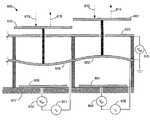
- a MEMS SLMis shown incorporating the electrostatic actuator shown in FIG. 5 .
- the SLM 600includes a discrete lower electrode ( 601 and 608 ) formed on a substrate 617 .
- Each pixelalso includes a center electrode ( 602 and 609 ) which is shown electrically in common across the SLM, i.e. the electrical ground.
- the SLM 600also includes an upper electrode 603 which is also electrically common across all pixels.
- the upper electrode 603 and the center electrodemay be formed as a single layer or a monolithic structure spanning the entire SLM.
- a bias voltage source 606serves to produce a bias voltage V B2 across the upper electrode layer 603 and the center electrode layer (including 602 and 609 ).
- the bias voltage V B1 across each of the lower/center electrode pairs per pixelis independent of all other bias voltages across the lower/center electrode pairs.
- a bias voltage V B1is initially produced by a bias voltage source 604 across the lower/center electrode pair 601 and 602 .
- a bias voltage V B1is also initially produced by a different bias voltage source 610 across the lower/center electrode pair 608 and 609 .
- independent driver voltage sourcesare provided such as shown by 605 and 611 .
- driver voltage source 605applies an additional driver voltage v a in series with the bias voltage V B1 of 604 and driver voltage source 611 applies an additional driver voltage v b in series with the bias voltage V B1 of 610 .
- Electrical connections to the electrodesmay be made through vias in the substrate 617 , as shown. In this manner, incident light at each pixel ( 613 - 616 ) may be independently modulated by only varying the driver voltage at each pixel, and not the bias voltages.
- FIG. 7a graph is shown for the present invention, characterizing displacement in response to a dynamically controlled voltage.
- the results of FIG. 7may be compared directly with that of FIG. 2 showing a similar graph for the two-electrode conventional design.
- the data presented in FIGS. 2 and 7are the result of research conducted at the Lawrence Livermore National Laboratory. Both graphs in FIGS. 2 and 7 are based on the following selected SLM parameters shown in Table 1, and representative of MEMS-scale SLMs.
- the SLM of the present inventioncan cause the same displacement as a conventional parallel plate actuator with less than half the driving voltage.
- the slope dv/dxvaries by a factor 30 for FIG. 2 of the conventional design, but only a factor of 4 in FIG. 7 of the present invention.
- the dynamic voltage rangeis 100V for FIG. 2, but less than 40V for FIG. 7 .
- the graph of FIG. 7also illustrates the substantial linearity of displacement response produced when a drive voltage is applied to the three-electrode actuator of the present invention.
- conventional two-electrode SLMsexhibit a highly non-linear response which must be compensated for through additional electronics.
- Such conventional SLM devicestherefore typically require high precision electronics drivers for adaptive control and error correction, further increasing complexity, size, and cost.
- reduction of the required variable voltage in the present inventionalso reduces the complexity, size and cost of the SLM electronics. In particular, it can lower power dissipation which may cause warpage, and also simplify the electronics by reducing the required voltage resolution (number of bits) due to a closer-to-linear phase vs. voltage characteristic.
Landscapes
- Physics & Mathematics (AREA)
- General Physics & Mathematics (AREA)
- Optics & Photonics (AREA)
- Mechanical Light Control Or Optical Switches (AREA)
Abstract
Description
| TABLE 1 | |||
| Parameter | Value | ||
| Pixel size (μm) | 300 | ||
| Effective pixel thickness (μm) | 5 | ||
| Gap-1 (μm) | 4.5 | ||
| Gap-2 (μm) | 4.5 | ||
| k (N/m) | 352 | ||
| V-bias (V) | 70 | ||
| Tres(μm) | 10 | ||
Claims (27)
Priority Applications (1)
| Application Number | Priority Date | Filing Date | Title |
|---|---|---|---|
| US10/340,317US6791735B2 (en) | 2002-01-09 | 2003-01-09 | Differentially-driven MEMS spatial light modulator |
Applications Claiming Priority (2)
| Application Number | Priority Date | Filing Date | Title |
|---|---|---|---|
| US34730002P | 2002-01-09 | 2002-01-09 | |
| US10/340,317US6791735B2 (en) | 2002-01-09 | 2003-01-09 | Differentially-driven MEMS spatial light modulator |
Publications (2)
| Publication Number | Publication Date |
|---|---|
| US20040008396A1 US20040008396A1 (en) | 2004-01-15 |
| US6791735B2true US6791735B2 (en) | 2004-09-14 |
Family
ID=30118034
Family Applications (1)
| Application Number | Title | Priority Date | Filing Date |
|---|---|---|---|
| US10/340,317Expired - Fee RelatedUS6791735B2 (en) | 2002-01-09 | 2003-01-09 | Differentially-driven MEMS spatial light modulator |
Country Status (1)
| Country | Link |
|---|---|
| US (1) | US6791735B2 (en) |
Cited By (22)
| Publication number | Priority date | Publication date | Assignee | Title |
|---|---|---|---|---|
| US20040232535A1 (en)* | 2003-05-22 | 2004-11-25 | Terry Tarn | Microelectromechanical device packages with integral heaters |
| US20050111119A1 (en)* | 2003-09-29 | 2005-05-26 | The Regents Of The University Of California | Double hidden flexure microactuator for phase mirror array |
| US20050180033A1 (en)* | 2004-02-13 | 2005-08-18 | Peter Kurczynski | Monolithic microelectromechanical system mirror |
| US20060022966A1 (en)* | 2004-07-29 | 2006-02-02 | Mar Eugene J | Method and system for controlling the output of a diffractive light device |
| US20060220045A1 (en)* | 2005-04-05 | 2006-10-05 | Jonathan Doan | Micromirror array device with compliant adhesive |
| US20060220199A1 (en)* | 2005-04-05 | 2006-10-05 | Duboc Robert M | Low cost hermetically sealed package |
| US20060267449A1 (en)* | 2005-05-27 | 2006-11-30 | Aksyuk Vladimir A | Torsional electrostatic actuator |
| US7164199B2 (en) | 2003-10-30 | 2007-01-16 | Texas Instruments Incorporated | Device packages with low stress assembly process |
| US20080001913A1 (en)* | 2006-06-30 | 2008-01-03 | Faase Kenneth J | MEMS device having distance stops |
| US20080121503A1 (en)* | 2006-11-02 | 2008-05-29 | Sampsell Jeffrey B | Compatible MEMS switch architecture |
| US20090068781A1 (en)* | 2004-05-04 | 2009-03-12 | Idc, Llc | Method of manufacture for microelectromechanical devices |
| US7612932B2 (en)* | 2004-09-27 | 2009-11-03 | Idc, Llc | Microelectromechanical device with optical function separated from mechanical and electrical function |
| US7630121B2 (en) | 2007-07-02 | 2009-12-08 | Qualcomm Mems Technologies, Inc. | Electromechanical device with optical function separated from mechanical and electrical function |
| WO2010071635A1 (en)* | 2008-12-16 | 2010-06-24 | Hewlett-Packard Development Company, L.P. | Spatial light modulator |
| US7791027B2 (en) | 2006-01-31 | 2010-09-07 | Ahura Scientific Inc. | Apparatus and method providing a hand-held spectrometer |
| US7952787B2 (en) | 2006-06-30 | 2011-05-31 | Qualcomm Mems Technologies, Inc. | Method of manufacturing MEMS devices providing air gap control |
| US7982700B2 (en) | 2004-09-27 | 2011-07-19 | Qualcomm Mems Technologies, Inc. | Conductive bus structure for interferometric modulator array |
| US20140071516A1 (en)* | 2009-06-15 | 2014-03-13 | Qualcomm Mems Technologies, Inc. | Analog interferometric modulator |
| US8817357B2 (en) | 2010-04-09 | 2014-08-26 | Qualcomm Mems Technologies, Inc. | Mechanical layer and methods of forming the same |
| US9097885B2 (en) | 2004-09-27 | 2015-08-04 | Qualcomm Mems Technologies, Inc. | Device having a conductive light absorbing mask and method for fabricating same |
| US9305497B2 (en) | 2012-08-31 | 2016-04-05 | Qualcomm Mems Technologies, Inc. | Systems, devices, and methods for driving an analog interferometric modulator |
| US9910268B2 (en)* | 2013-11-27 | 2018-03-06 | Nikon Corporation | Spatial light modulator, photolithographing apparatus, exposure apparatus, and method of manufacturing device |
Families Citing this family (140)
| Publication number | Priority date | Publication date | Assignee | Title |
|---|---|---|---|---|
| US7123216B1 (en)* | 1994-05-05 | 2006-10-17 | Idc, Llc | Photonic MEMS and structures |
| US7471444B2 (en)* | 1996-12-19 | 2008-12-30 | Idc, Llc | Interferometric modulation of radiation |
| US7532377B2 (en) | 1998-04-08 | 2009-05-12 | Idc, Llc | Movable micro-electromechanical device |
| WO1999052006A2 (en)* | 1998-04-08 | 1999-10-14 | Etalon, Inc. | Interferometric modulation of radiation |
| WO2003007049A1 (en) | 1999-10-05 | 2003-01-23 | Iridigm Display Corporation | Photonic mems and structures |
| TW200413810A (en) | 2003-01-29 | 2004-08-01 | Prime View Int Co Ltd | Light interference display panel and its manufacturing method |
| TW200506479A (en)* | 2003-08-15 | 2005-02-16 | Prime View Int Co Ltd | Color changeable pixel for an interference display |
| US7142346B2 (en)* | 2003-12-09 | 2006-11-28 | Idc, Llc | System and method for addressing a MEMS display |
| US7161728B2 (en)* | 2003-12-09 | 2007-01-09 | Idc, Llc | Area array modulation and lead reduction in interferometric modulators |
| US7245285B2 (en)* | 2004-04-28 | 2007-07-17 | Hewlett-Packard Development Company, L.P. | Pixel device |
| DE102005018604A1 (en)* | 2004-04-29 | 2005-11-24 | Samsung Electro-Mechanics Co., Ltd., Suwon | Open hole-based diffractive light modulator used in e.g. optical memory, has upper micromirror comprising open holes at center, such that it reflects/diffracts incident light based on height difference between upper and lower micromirrors |
| KR100871013B1 (en)* | 2004-06-25 | 2008-11-27 | 삼성전기주식회사 | Low Voltage Optical Modulator Drive Module |
| TWI233916B (en)* | 2004-07-09 | 2005-06-11 | Prime View Int Co Ltd | A structure of a micro electro mechanical system |
| EP2246726B1 (en)* | 2004-07-29 | 2013-04-03 | QUALCOMM MEMS Technologies, Inc. | System and method for micro-electromechanical operating of an interferometric modulator |
| US7889163B2 (en) | 2004-08-27 | 2011-02-15 | Qualcomm Mems Technologies, Inc. | Drive method for MEMS devices |
| US7499208B2 (en)* | 2004-08-27 | 2009-03-03 | Udc, Llc | Current mode display driver circuit realization feature |
| US7560299B2 (en)* | 2004-08-27 | 2009-07-14 | Idc, Llc | Systems and methods of actuating MEMS display elements |
| US7551159B2 (en)* | 2004-08-27 | 2009-06-23 | Idc, Llc | System and method of sensing actuation and release voltages of an interferometric modulator |
| US7515147B2 (en)* | 2004-08-27 | 2009-04-07 | Idc, Llc | Staggered column drive circuit systems and methods |
| US8878825B2 (en)* | 2004-09-27 | 2014-11-04 | Qualcomm Mems Technologies, Inc. | System and method for providing a variable refresh rate of an interferometric modulator display |
| US20060066594A1 (en)* | 2004-09-27 | 2006-03-30 | Karen Tyger | Systems and methods for driving a bi-stable display element |
| US7684104B2 (en) | 2004-09-27 | 2010-03-23 | Idc, Llc | MEMS using filler material and method |
| US7327510B2 (en)* | 2004-09-27 | 2008-02-05 | Idc, Llc | Process for modifying offset voltage characteristics of an interferometric modulator |
| US7545550B2 (en)* | 2004-09-27 | 2009-06-09 | Idc, Llc | Systems and methods of actuating MEMS display elements |
| US7417783B2 (en)* | 2004-09-27 | 2008-08-26 | Idc, Llc | Mirror and mirror layer for optical modulator and method |
| US7675669B2 (en) | 2004-09-27 | 2010-03-09 | Qualcomm Mems Technologies, Inc. | Method and system for driving interferometric modulators |
| US7893919B2 (en)* | 2004-09-27 | 2011-02-22 | Qualcomm Mems Technologies, Inc. | Display region architectures |
| US7304784B2 (en)* | 2004-09-27 | 2007-12-04 | Idc, Llc | Reflective display device having viewable display on both sides |
| US7446927B2 (en) | 2004-09-27 | 2008-11-04 | Idc, Llc | MEMS switch with set and latch electrodes |
| US7626581B2 (en)* | 2004-09-27 | 2009-12-01 | Idc, Llc | Device and method for display memory using manipulation of mechanical response |
| US7679627B2 (en)* | 2004-09-27 | 2010-03-16 | Qualcomm Mems Technologies, Inc. | Controller and driver features for bi-stable display |
| US7310179B2 (en)* | 2004-09-27 | 2007-12-18 | Idc, Llc | Method and device for selective adjustment of hysteresis window |
| US8008736B2 (en)* | 2004-09-27 | 2011-08-30 | Qualcomm Mems Technologies, Inc. | Analog interferometric modulator device |
| US7527995B2 (en)* | 2004-09-27 | 2009-05-05 | Qualcomm Mems Technologies, Inc. | Method of making prestructure for MEMS systems |
| US7843410B2 (en) | 2004-09-27 | 2010-11-30 | Qualcomm Mems Technologies, Inc. | Method and device for electrically programmable display |
| US7136213B2 (en)* | 2004-09-27 | 2006-11-14 | Idc, Llc | Interferometric modulators having charge persistence |
| US7369296B2 (en)* | 2004-09-27 | 2008-05-06 | Idc, Llc | Device and method for modifying actuation voltage thresholds of a deformable membrane in an interferometric modulator |
| US7564612B2 (en)* | 2004-09-27 | 2009-07-21 | Idc, Llc | Photonic MEMS and structures |
| US7372613B2 (en)* | 2004-09-27 | 2008-05-13 | Idc, Llc | Method and device for multistate interferometric light modulation |
| US7944599B2 (en)* | 2004-09-27 | 2011-05-17 | Qualcomm Mems Technologies, Inc. | Electromechanical device with optical function separated from mechanical and electrical function |
| US7302157B2 (en)* | 2004-09-27 | 2007-11-27 | Idc, Llc | System and method for multi-level brightness in interferometric modulation |
| US7130104B2 (en)* | 2004-09-27 | 2006-10-31 | Idc, Llc | Methods and devices for inhibiting tilting of a mirror in an interferometric modulator |
| US7321456B2 (en)* | 2004-09-27 | 2008-01-22 | Idc, Llc | Method and device for corner interferometric modulation |
| US7345805B2 (en) | 2004-09-27 | 2008-03-18 | Idc, Llc | Interferometric modulator array with integrated MEMS electrical switches |
| US7583429B2 (en) | 2004-09-27 | 2009-09-01 | Idc, Llc | Ornamental display device |
| US7554714B2 (en)* | 2004-09-27 | 2009-06-30 | Idc, Llc | Device and method for manipulation of thermal response in a modulator |
| US7719500B2 (en)* | 2004-09-27 | 2010-05-18 | Qualcomm Mems Technologies, Inc. | Reflective display pixels arranged in non-rectangular arrays |
| US7630119B2 (en)* | 2004-09-27 | 2009-12-08 | Qualcomm Mems Technologies, Inc. | Apparatus and method for reducing slippage between structures in an interferometric modulator |
| US8310441B2 (en) | 2004-09-27 | 2012-11-13 | Qualcomm Mems Technologies, Inc. | Method and system for writing data to MEMS display elements |
| US7936497B2 (en)* | 2004-09-27 | 2011-05-03 | Qualcomm Mems Technologies, Inc. | MEMS device having deformable membrane characterized by mechanical persistence |
| US7532195B2 (en)* | 2004-09-27 | 2009-05-12 | Idc, Llc | Method and system for reducing power consumption in a display |
| AU2005289445A1 (en)* | 2004-09-27 | 2006-04-06 | Idc, Llc | Method and device for multistate interferometric light modulation |
| US7724993B2 (en) | 2004-09-27 | 2010-05-25 | Qualcomm Mems Technologies, Inc. | MEMS switches with deforming membranes |
| KR100815338B1 (en) | 2004-10-08 | 2008-03-19 | 삼성전기주식회사 | Low Voltage Diffraction Optical Modulator |
| US7230749B2 (en)* | 2005-02-18 | 2007-06-12 | Hewlett-Packard Development Company, L.P. | Light blocking electrical interconnect |
| US7948457B2 (en)* | 2005-05-05 | 2011-05-24 | Qualcomm Mems Technologies, Inc. | Systems and methods of actuating MEMS display elements |
| US7920136B2 (en)* | 2005-05-05 | 2011-04-05 | Qualcomm Mems Technologies, Inc. | System and method of driving a MEMS display device |
| EP1878001A1 (en) | 2005-05-05 | 2008-01-16 | QUALCOMM Incorporated, Inc. | Dynamic driver ic and display panel configuration |
| US7884989B2 (en) | 2005-05-27 | 2011-02-08 | Qualcomm Mems Technologies, Inc. | White interferometric modulators and methods for forming the same |
| US7460292B2 (en) | 2005-06-03 | 2008-12-02 | Qualcomm Mems Technologies, Inc. | Interferometric modulator with internal polarization and drive method |
| EP2495212A3 (en)* | 2005-07-22 | 2012-10-31 | QUALCOMM MEMS Technologies, Inc. | Mems devices having support structures and methods of fabricating the same |
| KR101375337B1 (en) | 2005-07-22 | 2014-03-18 | 퀄컴 엠이엠에스 테크놀로지스, 인크. | Electomechanical devices having support structures and methods of fabricating the same |
| US7355779B2 (en) | 2005-09-02 | 2008-04-08 | Idc, Llc | Method and system for driving MEMS display elements |
| US7834829B2 (en)* | 2005-10-03 | 2010-11-16 | Hewlett-Packard Development Company, L.P. | Control circuit for overcoming stiction |
| GB0521251D0 (en) | 2005-10-19 | 2005-11-30 | Qinetiq Ltd | Optical modulation |
| US20070097476A1 (en)* | 2005-10-28 | 2007-05-03 | Truninger Martha A | Display system having a charge-controlled spatial light-modulator |
| US7630114B2 (en)* | 2005-10-28 | 2009-12-08 | Idc, Llc | Diffusion barrier layer for MEMS devices |
| US20070126673A1 (en)* | 2005-12-07 | 2007-06-07 | Kostadin Djordjev | Method and system for writing data to MEMS display elements |
| US8391630B2 (en)* | 2005-12-22 | 2013-03-05 | Qualcomm Mems Technologies, Inc. | System and method for power reduction when decompressing video streams for interferometric modulator displays |
| US7916980B2 (en) | 2006-01-13 | 2011-03-29 | Qualcomm Mems Technologies, Inc. | Interconnect structure for MEMS device |
| US7382515B2 (en)* | 2006-01-18 | 2008-06-03 | Qualcomm Mems Technologies, Inc. | Silicon-rich silicon nitrides as etch stops in MEMS manufacture |
| US8194056B2 (en)* | 2006-02-09 | 2012-06-05 | Qualcomm Mems Technologies Inc. | Method and system for writing data to MEMS display elements |
| US7550810B2 (en)* | 2006-02-23 | 2009-06-23 | Qualcomm Mems Technologies, Inc. | MEMS device having a layer movable at asymmetric rates |
| US7623287B2 (en)* | 2006-04-19 | 2009-11-24 | Qualcomm Mems Technologies, Inc. | Non-planar surface structures and process for microelectromechanical systems |
| US7417784B2 (en) | 2006-04-19 | 2008-08-26 | Qualcomm Mems Technologies, Inc. | Microelectromechanical device and method utilizing a porous surface |
| US7711239B2 (en)* | 2006-04-19 | 2010-05-04 | Qualcomm Mems Technologies, Inc. | Microelectromechanical device and method utilizing nanoparticles |
| US8049713B2 (en)* | 2006-04-24 | 2011-11-01 | Qualcomm Mems Technologies, Inc. | Power consumption optimized display update |
| US7649671B2 (en)* | 2006-06-01 | 2010-01-19 | Qualcomm Mems Technologies, Inc. | Analog interferometric modulator device with electrostatic actuation and release |
| US7471442B2 (en) | 2006-06-15 | 2008-12-30 | Qualcomm Mems Technologies, Inc. | Method and apparatus for low range bit depth enhancements for MEMS display architectures |
| US7702192B2 (en) | 2006-06-21 | 2010-04-20 | Qualcomm Mems Technologies, Inc. | Systems and methods for driving MEMS display |
| US7385744B2 (en)* | 2006-06-28 | 2008-06-10 | Qualcomm Mems Technologies, Inc. | Support structure for free-standing MEMS device and methods for forming the same |
| US7835061B2 (en)* | 2006-06-28 | 2010-11-16 | Qualcomm Mems Technologies, Inc. | Support structures for free-standing electromechanical devices |
| US7777715B2 (en) | 2006-06-29 | 2010-08-17 | Qualcomm Mems Technologies, Inc. | Passive circuits for de-multiplexing display inputs |
| US20080043315A1 (en)* | 2006-08-15 | 2008-02-21 | Cummings William J | High profile contacts for microelectromechanical systems |
| US7629197B2 (en)* | 2006-10-18 | 2009-12-08 | Qualcomm Mems Technologies, Inc. | Spatial light modulator |
| US7545552B2 (en)* | 2006-10-19 | 2009-06-09 | Qualcomm Mems Technologies, Inc. | Sacrificial spacer process and resultant structure for MEMS support structure |
| US7706042B2 (en) | 2006-12-20 | 2010-04-27 | Qualcomm Mems Technologies, Inc. | MEMS device and interconnects for same |
| US8115987B2 (en)* | 2007-02-01 | 2012-02-14 | Qualcomm Mems Technologies, Inc. | Modulating the intensity of light from an interferometric reflector |
| US7742220B2 (en)* | 2007-03-28 | 2010-06-22 | Qualcomm Mems Technologies, Inc. | Microelectromechanical device and method utilizing conducting layers separated by stops |
| US7715085B2 (en)* | 2007-05-09 | 2010-05-11 | Qualcomm Mems Technologies, Inc. | Electromechanical system having a dielectric movable membrane and a mirror |
| US7643202B2 (en)* | 2007-05-09 | 2010-01-05 | Qualcomm Mems Technologies, Inc. | Microelectromechanical system having a dielectric movable membrane and a mirror |
| US7719752B2 (en) | 2007-05-11 | 2010-05-18 | Qualcomm Mems Technologies, Inc. | MEMS structures, methods of fabricating MEMS components on separate substrates and assembly of same |
| US7625825B2 (en)* | 2007-06-14 | 2009-12-01 | Qualcomm Mems Technologies, Inc. | Method of patterning mechanical layer for MEMS structures |
| US7643199B2 (en) | 2007-06-19 | 2010-01-05 | Qualcomm Mems Technologies, Inc. | High aperture-ratio top-reflective AM-iMod displays |
| US7782517B2 (en)* | 2007-06-21 | 2010-08-24 | Qualcomm Mems Technologies, Inc. | Infrared and dual mode displays |
| US8068268B2 (en)* | 2007-07-03 | 2011-11-29 | Qualcomm Mems Technologies, Inc. | MEMS devices having improved uniformity and methods for making them |
| EP2183623A1 (en) | 2007-07-31 | 2010-05-12 | Qualcomm Mems Technologies, Inc. | Devices for enhancing colour shift of interferometric modulators |
| US8072402B2 (en)* | 2007-08-29 | 2011-12-06 | Qualcomm Mems Technologies, Inc. | Interferometric optical modulator with broadband reflection characteristics |
| US7773286B2 (en)* | 2007-09-14 | 2010-08-10 | Qualcomm Mems Technologies, Inc. | Periodic dimple array |
| US7847999B2 (en)* | 2007-09-14 | 2010-12-07 | Qualcomm Mems Technologies, Inc. | Interferometric modulator display devices |
| US20090078316A1 (en)* | 2007-09-24 | 2009-03-26 | Qualcomm Incorporated | Interferometric photovoltaic cell |
| US8058549B2 (en)* | 2007-10-19 | 2011-11-15 | Qualcomm Mems Technologies, Inc. | Photovoltaic devices with integrated color interferometric film stacks |
| CN101828145B (en)* | 2007-10-19 | 2012-03-21 | 高通Mems科技公司 | Displays with integrated photovoltaic elements |
| EP2203765A1 (en)* | 2007-10-23 | 2010-07-07 | Qualcomm Mems Technologies, Inc. | Adjustably transmissive mems-based devices |
| US20090293955A1 (en)* | 2007-11-07 | 2009-12-03 | Qualcomm Incorporated | Photovoltaics with interferometric masks |
| US8941631B2 (en)* | 2007-11-16 | 2015-01-27 | Qualcomm Mems Technologies, Inc. | Simultaneous light collection and illumination on an active display |
| US7715079B2 (en)* | 2007-12-07 | 2010-05-11 | Qualcomm Mems Technologies, Inc. | MEMS devices requiring no mechanical support |
| WO2009085601A2 (en)* | 2007-12-21 | 2009-07-09 | Qualcom Mems Technologies, Inc. | Multijunction photovoltaic cells |
| US7863079B2 (en) | 2008-02-05 | 2011-01-04 | Qualcomm Mems Technologies, Inc. | Methods of reducing CD loss in a microelectromechanical device |
| EP2252991A1 (en)* | 2008-02-11 | 2010-11-24 | QUALCOMM MEMS Technologies, Inc. | Method and apparatus for sensing, measurement or characterization of display elements integrated with the display drive scheme, and system and applications using the same |
| US8164821B2 (en) | 2008-02-22 | 2012-04-24 | Qualcomm Mems Technologies, Inc. | Microelectromechanical device with thermal expansion balancing layer or stiffening layer |
| US7944604B2 (en) | 2008-03-07 | 2011-05-17 | Qualcomm Mems Technologies, Inc. | Interferometric modulator in transmission mode |
| US7612933B2 (en)* | 2008-03-27 | 2009-11-03 | Qualcomm Mems Technologies, Inc. | Microelectromechanical device with spacing layer |
| US7898723B2 (en)* | 2008-04-02 | 2011-03-01 | Qualcomm Mems Technologies, Inc. | Microelectromechanical systems display element with photovoltaic structure |
| US7969638B2 (en) | 2008-04-10 | 2011-06-28 | Qualcomm Mems Technologies, Inc. | Device having thin black mask and method of fabricating the same |
| US7768690B2 (en) | 2008-06-25 | 2010-08-03 | Qualcomm Mems Technologies, Inc. | Backlight displays |
| US7746539B2 (en)* | 2008-06-25 | 2010-06-29 | Qualcomm Mems Technologies, Inc. | Method for packing a display device and the device obtained thereof |
| US8023167B2 (en)* | 2008-06-25 | 2011-09-20 | Qualcomm Mems Technologies, Inc. | Backlight displays |
| US7859740B2 (en)* | 2008-07-11 | 2010-12-28 | Qualcomm Mems Technologies, Inc. | Stiction mitigation with integrated mech micro-cantilevers through vertical stress gradient control |
| US7855826B2 (en) | 2008-08-12 | 2010-12-21 | Qualcomm Mems Technologies, Inc. | Method and apparatus to reduce or eliminate stiction and image retention in interferometric modulator devices |
| US8358266B2 (en)* | 2008-09-02 | 2013-01-22 | Qualcomm Mems Technologies, Inc. | Light turning device with prismatic light turning features |
| WO2010044901A1 (en)* | 2008-10-16 | 2010-04-22 | Qualcomm Mems Technologies, Inc. | Monolithic imod color enhanced photovoltaic cell |
| US20100096011A1 (en)* | 2008-10-16 | 2010-04-22 | Qualcomm Mems Technologies, Inc. | High efficiency interferometric color filters for photovoltaic modules |
| DE102008043836A1 (en) | 2008-11-19 | 2010-05-20 | Robert Bosch Gmbh | Method of operating an electrostatic drive and electrostatic drives |
| US8270056B2 (en)* | 2009-03-23 | 2012-09-18 | Qualcomm Mems Technologies, Inc. | Display device with openings between sub-pixels and method of making same |
| US8736590B2 (en)* | 2009-03-27 | 2014-05-27 | Qualcomm Mems Technologies, Inc. | Low voltage driver scheme for interferometric modulators |
| CN102449512A (en)* | 2009-05-29 | 2012-05-09 | 高通Mems科技公司 | Illumination devices and methods of fabrication thereof |
| US8270062B2 (en)* | 2009-09-17 | 2012-09-18 | Qualcomm Mems Technologies, Inc. | Display device with at least one movable stop element |
| US8488228B2 (en)* | 2009-09-28 | 2013-07-16 | Qualcomm Mems Technologies, Inc. | Interferometric display with interferometric reflector |
| CN103109315A (en)* | 2010-08-17 | 2013-05-15 | 高通Mems科技公司 | Actuation and calibration of a charge neutral electrode in an interferometric display device |
| US9057872B2 (en) | 2010-08-31 | 2015-06-16 | Qualcomm Mems Technologies, Inc. | Dielectric enhanced mirror for IMOD display |
| US9134527B2 (en) | 2011-04-04 | 2015-09-15 | Qualcomm Mems Technologies, Inc. | Pixel via and methods of forming the same |
| US8963159B2 (en) | 2011-04-04 | 2015-02-24 | Qualcomm Mems Technologies, Inc. | Pixel via and methods of forming the same |
| US8659816B2 (en) | 2011-04-25 | 2014-02-25 | Qualcomm Mems Technologies, Inc. | Mechanical layer and methods of making the same |
| US8736939B2 (en) | 2011-11-04 | 2014-05-27 | Qualcomm Mems Technologies, Inc. | Matching layer thin-films for an electromechanical systems reflective display device |
| US8847862B2 (en) | 2011-11-29 | 2014-09-30 | Qualcomm Mems Technologies, Inc. | Systems, devices, and methods for driving an interferometric modulator |
| US8669926B2 (en)* | 2011-11-30 | 2014-03-11 | Qualcomm Mems Technologies, Inc. | Drive scheme for a display |
| US12160084B2 (en) | 2019-10-15 | 2024-12-03 | Texas Instruments Incorporated | MEMS-based phase spatial light modulating architecture |
| US12339437B2 (en)* | 2019-12-12 | 2025-06-24 | Texas Instruments Incorporated | Bias voltage adjustment for a phase light modulator |
| CN112038091B (en)* | 2020-08-04 | 2022-08-19 | 厚元技术(香港)有限公司 | Adjustable capacitor based on MEMS structure |
Citations (4)
| Publication number | Priority date | Publication date | Assignee | Title |
|---|---|---|---|---|
| US5771321A (en)* | 1996-01-04 | 1998-06-23 | Massachusetts Institute Of Technology | Micromechanical optical switch and flat panel display |
| US6329738B1 (en)* | 1999-03-30 | 2001-12-11 | Massachusetts Institute Of Technology | Precision electrostatic actuation and positioning |
| US6433917B1 (en)* | 2000-11-22 | 2002-08-13 | Ball Semiconductor, Inc. | Light modulation device and system |
| US6438282B1 (en)* | 1998-01-20 | 2002-08-20 | Seiko Epson Corporation | Optical switching device and image display device |
- 2003
- 2003-01-09USUS10/340,317patent/US6791735B2/ennot_activeExpired - Fee Related
Patent Citations (4)
| Publication number | Priority date | Publication date | Assignee | Title |
|---|---|---|---|---|
| US5771321A (en)* | 1996-01-04 | 1998-06-23 | Massachusetts Institute Of Technology | Micromechanical optical switch and flat panel display |
| US6438282B1 (en)* | 1998-01-20 | 2002-08-20 | Seiko Epson Corporation | Optical switching device and image display device |
| US6329738B1 (en)* | 1999-03-30 | 2001-12-11 | Massachusetts Institute Of Technology | Precision electrostatic actuation and positioning |
| US6433917B1 (en)* | 2000-11-22 | 2002-08-13 | Ball Semiconductor, Inc. | Light modulation device and system |
Cited By (47)
| Publication number | Priority date | Publication date | Assignee | Title |
|---|---|---|---|---|
| US7402878B2 (en) | 2003-05-22 | 2008-07-22 | Texas Instruments Incorporated | Packaging method for microstructure and semiconductor devices |
| US20040238600A1 (en)* | 2003-05-22 | 2004-12-02 | Terry Tarn | Novel packaging method for microstructure and semiconductor devices |
| US20050157374A1 (en)* | 2003-05-22 | 2005-07-21 | Terry Tarn | Microelectromechanical device packages with integral heaters |
| US7449773B2 (en) | 2003-05-22 | 2008-11-11 | Texas Instruments Incorporated | Microelectromechanical device packages with integral heaters |
| US20050185248A1 (en)* | 2003-05-22 | 2005-08-25 | Terry Tarn | Microelectromechanical device packages with integral heaters |
| US7282393B2 (en) | 2003-05-22 | 2007-10-16 | Texas Instruments Incorporated | Microelectromechanical device packages with integral heaters |
| US9056764B2 (en) | 2003-05-22 | 2015-06-16 | Texas Instruments Incorporated | Microelectromechanical device packages with integral heaters |
| US20040232535A1 (en)* | 2003-05-22 | 2004-11-25 | Terry Tarn | Microelectromechanical device packages with integral heaters |
| US7872338B2 (en) | 2003-05-22 | 2011-01-18 | Texas Instruments Incorporated | Microelectromechanical device packages with integral heaters |
| US20090072380A1 (en)* | 2003-05-22 | 2009-03-19 | Texas Instruments Incorporated | Microelectromechanical Device Packages with Integral Heaters |
| US20050111119A1 (en)* | 2003-09-29 | 2005-05-26 | The Regents Of The University Of California | Double hidden flexure microactuator for phase mirror array |
| US7075699B2 (en)* | 2003-09-29 | 2006-07-11 | The Regents Of The University Of California | Double hidden flexure microactuator for phase mirror array |
| US7164199B2 (en) | 2003-10-30 | 2007-01-16 | Texas Instruments Incorporated | Device packages with low stress assembly process |
| US20050180033A1 (en)* | 2004-02-13 | 2005-08-18 | Peter Kurczynski | Monolithic microelectromechanical system mirror |
| US7704772B2 (en) | 2004-05-04 | 2010-04-27 | Qualcomm Mems Technologies, Inc. | Method of manufacture for microelectromechanical devices |
| US20090068781A1 (en)* | 2004-05-04 | 2009-03-12 | Idc, Llc | Method of manufacture for microelectromechanical devices |
| US20060022966A1 (en)* | 2004-07-29 | 2006-02-02 | Mar Eugene J | Method and system for controlling the output of a diffractive light device |
| US7436389B2 (en)* | 2004-07-29 | 2008-10-14 | Eugene J Mar | Method and system for controlling the output of a diffractive light device |
| US7982700B2 (en) | 2004-09-27 | 2011-07-19 | Qualcomm Mems Technologies, Inc. | Conductive bus structure for interferometric modulator array |
| US9097885B2 (en) | 2004-09-27 | 2015-08-04 | Qualcomm Mems Technologies, Inc. | Device having a conductive light absorbing mask and method for fabricating same |
| US9086564B2 (en) | 2004-09-27 | 2015-07-21 | Qualcomm Mems Technologies, Inc. | Conductive bus structure for interferometric modulator array |
| US7612932B2 (en)* | 2004-09-27 | 2009-11-03 | Idc, Llc | Microelectromechanical device with optical function separated from mechanical and electrical function |
| US8390547B2 (en) | 2004-09-27 | 2013-03-05 | Qualcomm Mems Technologies, Inc. | Conductive bus structure for interferometric modulator array |
| US20060220199A1 (en)* | 2005-04-05 | 2006-10-05 | Duboc Robert M | Low cost hermetically sealed package |
| US7508063B2 (en) | 2005-04-05 | 2009-03-24 | Texas Instruments Incorporated | Low cost hermetically sealed package |
| US20060220045A1 (en)* | 2005-04-05 | 2006-10-05 | Jonathan Doan | Micromirror array device with compliant adhesive |
| US7408250B2 (en) | 2005-04-05 | 2008-08-05 | Texas Instruments Incorporated | Micromirror array device with compliant adhesive |
| US7253550B2 (en)* | 2005-05-27 | 2007-08-07 | Lucent Technologies Inc. | Torsional electrostatic actuator |
| US20060267449A1 (en)* | 2005-05-27 | 2006-11-30 | Aksyuk Vladimir A | Torsional electrostatic actuator |
| US7791027B2 (en) | 2006-01-31 | 2010-09-07 | Ahura Scientific Inc. | Apparatus and method providing a hand-held spectrometer |
| US8964280B2 (en) | 2006-06-30 | 2015-02-24 | Qualcomm Mems Technologies, Inc. | Method of manufacturing MEMS devices providing air gap control |
| US7952787B2 (en) | 2006-06-30 | 2011-05-31 | Qualcomm Mems Technologies, Inc. | Method of manufacturing MEMS devices providing air gap control |
| US7741751B2 (en)* | 2006-06-30 | 2010-06-22 | Hewlett-Packard Development Company, L.P. | MEMS device having distance stops |
| US8102590B2 (en) | 2006-06-30 | 2012-01-24 | Qualcomm Mems Technologies, Inc. | Method of manufacturing MEMS devices providing air gap control |
| US20080001913A1 (en)* | 2006-06-30 | 2008-01-03 | Faase Kenneth J | MEMS device having distance stops |
| US20080121503A1 (en)* | 2006-11-02 | 2008-05-29 | Sampsell Jeffrey B | Compatible MEMS switch architecture |
| US7684106B2 (en) | 2006-11-02 | 2010-03-23 | Qualcomm Mems Technologies, Inc. | Compatible MEMS switch architecture |
| US7630121B2 (en) | 2007-07-02 | 2009-12-08 | Qualcomm Mems Technologies, Inc. | Electromechanical device with optical function separated from mechanical and electrical function |
| US20110169815A1 (en)* | 2008-12-16 | 2011-07-14 | Hewlett-Packard Development Company, L.P. | Spatial light modulator |
| US8659510B2 (en) | 2008-12-16 | 2014-02-25 | Hewlett-Packard Development Company, L.P. | Spatial light modulator |
| WO2010071635A1 (en)* | 2008-12-16 | 2010-06-24 | Hewlett-Packard Development Company, L.P. | Spatial light modulator |
| US8879141B2 (en)* | 2009-06-15 | 2014-11-04 | Qualcomm Mems Technologies, Inc. | Analog interferometric modulator |
| US20140071516A1 (en)* | 2009-06-15 | 2014-03-13 | Qualcomm Mems Technologies, Inc. | Analog interferometric modulator |
| US8817357B2 (en) | 2010-04-09 | 2014-08-26 | Qualcomm Mems Technologies, Inc. | Mechanical layer and methods of forming the same |
| US9305497B2 (en) | 2012-08-31 | 2016-04-05 | Qualcomm Mems Technologies, Inc. | Systems, devices, and methods for driving an analog interferometric modulator |
| US9910268B2 (en)* | 2013-11-27 | 2018-03-06 | Nikon Corporation | Spatial light modulator, photolithographing apparatus, exposure apparatus, and method of manufacturing device |
| TWI646353B (en)* | 2013-11-27 | 2019-01-01 | 日商尼康股份有限公司 | Space light modulator, light drawing device, exposure device, and component manufacturing method |
Also Published As
| Publication number | Publication date |
|---|---|
| US20040008396A1 (en) | 2004-01-15 |
Similar Documents
| Publication | Publication Date | Title |
|---|---|---|
| US6791735B2 (en) | Differentially-driven MEMS spatial light modulator | |
| US6666561B1 (en) | Continuously variable analog micro-mirror device | |
| Hornbeck et al. | Bistable deformable mirror device | |
| US7075699B2 (en) | Double hidden flexure microactuator for phase mirror array | |
| US7158278B2 (en) | Display device based on bistable electrostatic shutter | |
| US5281887A (en) | Two independent spatial variable degree of freedom wavefront modulator | |
| US5835256A (en) | Reflective spatial light modulator with encapsulated micro-mechanical elements | |
| CN101151206B (en) | Method and device for actuating a display | |
| US6327071B1 (en) | Drive methods of array-type light modulation element and flat-panel display | |
| KR101157502B1 (en) | Methods and apparatus for actuating displays | |
| US20060227405A1 (en) | Microelectromechanical device with reset electrode | |
| US7733553B2 (en) | Light modulator with tunable optical state | |
| US5455709A (en) | Total internal reflection spatial light modulation apparatus and method of fabrication thereof | |
| US20060017689A1 (en) | Light modulator with concentric control-electrode structure | |
| US20030015936A1 (en) | Electrostatic actuator | |
| WO1998048310A1 (en) | Light valve target comprising electrostatically-repelled micro-mirrors | |
| WO2005106837A1 (en) | Optical pixel device | |
| JP2000352943A (en) | Super precision electromechanic shutter assembly and forming method for the same | |
| JP2002277771A (en) | Light modulator | |
| US7573631B1 (en) | Hybrid analog/digital spatial light modulator | |
| EP2015125A1 (en) | Optically controlled deformable mirror | |
| WO2002042825A1 (en) | Light modulation device and system | |
| US20060279831A1 (en) | Micro-electro mechanical light modulator device | |
| US7463403B1 (en) | High impedance drive circuit for a micro-electromechanical system device | |
| US5521746A (en) | Poppet valve modulator |
Legal Events
| Date | Code | Title | Description |
|---|---|---|---|
| AS | Assignment | Owner name:CALIFORNIA, THE REGENTS OF THE UNIVERSITY OF, CALI Free format text:ASSIGNMENT OF ASSIGNORS INTEREST;ASSIGNOR:STAPPAERTS, EDDY A.;REEL/FRAME:013674/0650 Effective date:20030109 Owner name:REGENTS OF THE UNIVERSITY OF CALIFORNIA, THE, CALI Free format text:ASSIGNMENT OF ASSIGNORS INTEREST;ASSIGNOR:STAPPAERTS, EDDY A.;REEL/FRAME:013674/0650 Effective date:20030109 | |
| AS | Assignment | Owner name:ENERGY, U.S. DEPARTMENT OF, CALIFORNIA Free format text:CONFIRMATORY LICENSE;ASSIGNOR:CALIFORNIA, REGENTS OF THE UNIVERSITY OF;REEL/FRAME:014370/0438 Effective date:20030328 | |
| FPAY | Fee payment | Year of fee payment:4 | |
| AS | Assignment | Owner name:LAWRENCE LIVERMORE NATIONAL SECURITY LLC, CALIFORN Free format text:ASSIGNMENT OF ASSIGNORS INTEREST;ASSIGNOR:THE REGENTS OF THE UNIVERSITY OF CALIFORNIA;REEL/FRAME:021217/0050 Effective date:20080623 | |
| REMI | Maintenance fee reminder mailed | ||
| LAPS | Lapse for failure to pay maintenance fees | ||
| STCH | Information on status: patent discontinuation | Free format text:PATENT EXPIRED DUE TO NONPAYMENT OF MAINTENANCE FEES UNDER 37 CFR 1.362 | |
| FP | Lapsed due to failure to pay maintenance fee | Effective date:20120914 |