US6791611B2 - Dual ported memory for digital image sensor - Google Patents
Dual ported memory for digital image sensorDownload PDFInfo
- Publication number
- US6791611B2 US6791611B2US09/864,296US86429601AUS6791611B2US 6791611 B2US6791611 B2US 6791611B2US 86429601 AUS86429601 AUS 86429601AUS 6791611 B2US6791611 B2US 6791611B2
- Authority
- US
- United States
- Prior art keywords
- data
- memory
- image sensor
- bus
- data bus
- Prior art date
- Legal status (The legal status is an assumption and is not a legal conclusion. Google has not performed a legal analysis and makes no representation as to the accuracy of the status listed.)
- Expired - Lifetime, expires
Links
- 230000015654memoryEffects0.000titleclaimsabstractdescription121
- 230000009977dual effectEffects0.000titledescription9
- 230000007246mechanismEffects0.000claimsdescription7
- 210000004027cellAnatomy0.000description16
- 238000000034methodMethods0.000description16
- 230000008569processEffects0.000description13
- 238000010586diagramMethods0.000description11
- 230000010354integrationEffects0.000description8
- 239000000872bufferSubstances0.000description6
- 230000008901benefitEffects0.000description5
- 239000003990capacitorSubstances0.000description5
- 238000006243chemical reactionMethods0.000description5
- 230000005540biological transmissionEffects0.000description3
- 238000012545processingMethods0.000description3
- 239000000758substrateSubstances0.000description3
- 230000006835compressionEffects0.000description2
- 238000007906compressionMethods0.000description2
- 238000013461designMethods0.000description2
- 230000006870functionEffects0.000description2
- 238000005070samplingMethods0.000description2
- 210000004460N cellAnatomy0.000description1
- 238000009825accumulationMethods0.000description1
- 238000013459approachMethods0.000description1
- 230000004888barrier functionEffects0.000description1
- 230000000295complement effectEffects0.000description1
- 230000001010compromised effectEffects0.000description1
- 230000008878couplingEffects0.000description1
- 238000010168coupling processMethods0.000description1
- 238000005859coupling reactionMethods0.000description1
- 230000007423decreaseEffects0.000description1
- 230000001419dependent effectEffects0.000description1
- 230000000694effectsEffects0.000description1
- 238000005516engineering processMethods0.000description1
- 230000003090exacerbative effectEffects0.000description1
- 230000003993interactionEffects0.000description1
- 230000006386memory functionEffects0.000description1
- 229910044991metal oxideInorganic materials0.000description1
- 150000004706metal oxidesChemical class0.000description1
- 238000004806packaging method and processMethods0.000description1
- 229920006395saturated elastomerPolymers0.000description1
- 239000004065semiconductorSubstances0.000description1
- 238000009416shutteringMethods0.000description1
- 238000001228spectrumMethods0.000description1
- 230000002459sustained effectEffects0.000description1
- 238000012546transferMethods0.000description1
- 238000001429visible spectrumMethods0.000description1
Images


Classifications
- H—ELECTRICITY
- H04—ELECTRIC COMMUNICATION TECHNIQUE
- H04N—PICTORIAL COMMUNICATION, e.g. TELEVISION
- H04N1/00—Scanning, transmission or reproduction of documents or the like, e.g. facsimile transmission; Details thereof
- H04N1/00127—Connection or combination of a still picture apparatus with another apparatus, e.g. for storage, processing or transmission of still picture signals or of information associated with a still picture
- H04N1/00281—Connection or combination of a still picture apparatus with another apparatus, e.g. for storage, processing or transmission of still picture signals or of information associated with a still picture with a telecommunication apparatus, e.g. a switched network of teleprinters for the distribution of text-based information, a selective call terminal
- H04N1/00307—Connection or combination of a still picture apparatus with another apparatus, e.g. for storage, processing or transmission of still picture signals or of information associated with a still picture with a telecommunication apparatus, e.g. a switched network of teleprinters for the distribution of text-based information, a selective call terminal with a mobile telephone apparatus
- H—ELECTRICITY
- H04—ELECTRIC COMMUNICATION TECHNIQUE
- H04N—PICTORIAL COMMUNICATION, e.g. TELEVISION
- H04N23/00—Cameras or camera modules comprising electronic image sensors; Control thereof
- H04N23/70—Circuitry for compensating brightness variation in the scene
- H—ELECTRICITY
- H04—ELECTRIC COMMUNICATION TECHNIQUE
- H04N—PICTORIAL COMMUNICATION, e.g. TELEVISION
- H04N23/00—Cameras or camera modules comprising electronic image sensors; Control thereof
- H04N23/70—Circuitry for compensating brightness variation in the scene
- H04N23/741—Circuitry for compensating brightness variation in the scene by increasing the dynamic range of the image compared to the dynamic range of the electronic image sensors
- H—ELECTRICITY
- H04—ELECTRIC COMMUNICATION TECHNIQUE
- H04N—PICTORIAL COMMUNICATION, e.g. TELEVISION
- H04N25/00—Circuitry of solid-state image sensors [SSIS]; Control thereof
- H—ELECTRICITY
- H04—ELECTRIC COMMUNICATION TECHNIQUE
- H04N—PICTORIAL COMMUNICATION, e.g. TELEVISION
- H04N25/00—Circuitry of solid-state image sensors [SSIS]; Control thereof
- H04N25/70—SSIS architectures; Circuits associated therewith
- H04N25/76—Addressed sensors, e.g. MOS or CMOS sensors
- H—ELECTRICITY
- H04—ELECTRIC COMMUNICATION TECHNIQUE
- H04N—PICTORIAL COMMUNICATION, e.g. TELEVISION
- H04N7/00—Television systems
- H04N7/14—Systems for two-way working
- H04N7/141—Systems for two-way working between two video terminals, e.g. videophone
- H04N7/142—Constructional details of the terminal equipment, e.g. arrangements of the camera and the display
- H—ELECTRICITY
- H04—ELECTRIC COMMUNICATION TECHNIQUE
- H04N—PICTORIAL COMMUNICATION, e.g. TELEVISION
- H04N2201/00—Indexing scheme relating to scanning, transmission or reproduction of documents or the like, and to details thereof
- H04N2201/0008—Connection or combination of a still picture apparatus with another apparatus
- H04N2201/0065—Converting image data to a format usable by the connected apparatus or vice versa
- H04N2201/0068—Converting from still picture data
Definitions
- the inventionrelates to image sensor systems. More particularly, the invention relates to a dual ported memory for a digital image sensor that fundamentally different from the traditional CCD/CMOS image sensors.
- Digital photographyis one of the most exciting technologies to have emerged during the twentieth century. With the appropriate hardware and software (and a little knowledge), anyone can put the principles of digital photography to work. Digital cameras, for example, are on the cutting edge of digital photography. Recent product introductions, technological advancements, and price cuts, along with the emergence of email and the World Wide Web, have helped make the digital cameras one of the hottest new categories of consumer electronics products.
- Digital camerasdo not work in the same way as traditional film cameras do. In fact, they are more closely related to computer scanners, copiers, or fax machines.
- Most digital camerasuse an image sensor or photosensitive device, such as charged-coupled device (CCD) or complementary metal-oxide semiconductor (CMOS) to sense a scene.
- CCDcharged-coupled device
- CMOScomplementary metal-oxide semiconductor
- the photosensitive devicereacts to light reflected from the scene and can translate the strength of that reaction into a numeric equivalent. By passing light through red, green, and blue filters, for example, the reaction can be gauged for each separate color spectrum.
- red, green, and blue filtersfor example, the reaction can be gauged for each separate color spectrum.
- the cameracan determine the specific color of each element of the picture. Because the image is actually a collection of numeric data, it can easily be downloaded into a computer and manipulated for more artistic effects.
- U.S. Pat. No. 5,461,425 by B. Fowler et aldiscloses a new type of image sensors that integrate pixel-level analog-to-digital conversion (ADC) with an area image sensor. Such integration helps lower system cost, power consumption and improve system performance. Among the different schemes for integrating the ADC with an area image sensor, pixel level ADC promises to achieve the lowest power, and the simplest, most process portable and scalable design.
- the ADC approach described in U.S. Pat. No. 5,461,425is based on first order sigma delta modulation which has the advantage of requiring fairly simple and robust circuits. Further with the digital values directly provided by each of the pixel elements, the readout of the digital values could be of extremely high.
- the high speed readoutcan be compromised by subsequent I/O bandwidth due to the limited speed provided by the off-chip memory or computing devices.
- image processingmust be performed by the system after the image data are transferred from the image sensor to a system memory. This consumes computing power, while exacerbating system latency.
- What is desiredis to provide a sensor architecture that provides the memory function and image processing features without compromising the readout speed from the digital pixels and without requiring significant additional compute power. This desire is fulfilled by the provision of both a memory and a processor on the same substrate as the image sensor.
- an image sensor architectureis provided to accommodate the relative mismatch of bus width between the image sensor, processor, and memory.
- the preferred embodiment of the inventionprovides a dual-ported memory structure having a relatively wide data port for receiving data from the image sensor and having a relatively narrow data port for communicating data to and from the processor.
- the memoryis organized into banks of a specific width. The banks may be accessed sequentially by the processor, such that the bus width is equivalent to the bank width, and the banks may be accessed simultaneously, such that the bus width is equivalent to the combined bank widths.
- a simple switching meansoperating under processor control, reconfigures the memory on the fly.
- an important object of the present inventionis to provide solutions of accommodating the relative mismatch of bus width between the image sensor, processor, and memory.
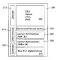
- FIG. 1Ais a block diagram that shows a CMOS image sensor or photosensitive chip in which the invention may be practiced
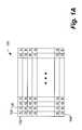
- FIG. 1Bis a block diagram which shows a photodiode modeled as a current source and a capacitor
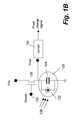
- FIG. 2is a block diagram which shows the architecture of a digital pixel sensor, as described in U.S. Pat. No. 5,461,425;
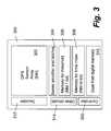
- FIG. 3is a block diagram which shows an image sensor that includes a threshold memory, a time index memory, a separate data memory, and a controller, where each of the memories and the digital pixel sensor are integrated into the same sensor, and where the processing of image data is accomplished within the image sensor itself according to the invention;
- FIG. 4Ais a block diagram of an image sensor architecture having a dual ported memory according to the invention.
- FIG. 4Bshows a block diagram of a dual ported memory updating mechanism according to one embodiment of the present invention.
- FIG. 5is a block diagram of an image sensor architecture showing a bank switching scheme for matching memory data bus width to disparate data buses according to the invention.
- FIG. 1Ashows an image sensor or photosensitive chip 100 in which the invention may be practiced.
- the image sensor 100may be used in an image capturing device (e.g. a digital camera) for either stationary or video photography, and produces signals representing the strength of light impinged thereupon.
- the photosensitive chip 100which is typically fabricated on a substrate such as CMOS, comprises a plurality of photodetectors that are arranged in a 2-dimensional array.
- a mosaic of selectively transmissive filtersis superimposed in registration with each of the photodetectors so that a first, second, and third selective group of photodetectors are made to sense three different color ranges, for example, the red, green, and blue range of the visible spectrum, respectively.
- the number of the photodetectors in the photosensitive chip 100typically determines the resolution of digital images resulting therefrom.
- the horizontal resolutionis a function of the number of photodetectors in a row 102
- the vertical resolutionis a function of the number of photodetectors in a column 104 .
- Each of the photodetectorscomprises a photosensor that produces an electronic signal when it is exposed to light.
- the photosensoris a photodiode or a photogate in a CMOS sensor.
- FIG. 1Bshows a photodiode 120 that is modeled as a current source 122 and a capacitor 124 .
- the capacitor 124is fully charged by and nearly to Vcc through the transistor 128 , at which point the photodiode 120 is ready for light integration.
- the capacitor 124is actually charged to Vcc-Vt, where Vt is a voltage across the transistor 128 .
- Vtis assumed to be nearly zero.
- the reset signalAs soon as the reset signal is dropped (i.e. the voltage level is changed), light integration starts. As more and more incident photons from light 126 strike the surface of the photodiode 120 , the current of current source 122 increases. The capacitor 124 starts to discharge through the current source 122 . Typically, the photodiode collects more photons for higher photon intensities and, as a result, the resistance of the resistor 122 decreases. Consequently, a faster discharge signal Vout is produced. In other words, the signal from Vout is proportional to the incident photons which strike the photodiode 120 . This signal is alternatively referred to herein as an electronic signal or pixel charge signal.
- a circuit 130may be employed to enhance the electronic signal Vout to a desired level so that the output, i.e. the pixel charge signal, is effectively coupled to following circuitry.
- the operation of an image sensorcomprises two processes: 1. the light integration process, as described above; and 2. the read out process. Each of these two processes is sustained for a controlled time interval.
- each photodetectoris initiated to accumulate incident photons of the light and the accumulation is reflected as a pixel charge signal.
- the photodetectorsstart the read out process during which the pixel charge signal in each photodetector is read out via read out circuitry to a data bus or video bus.
- the interval during which the light integration process proceedsis referred to as exposure control or electronic shuttering, and it controls how much charge is accumulated by each of the photodiodes.
- FIG. 2duplicates FIG. 1 of U.S. Pat. No. 5,461,425 and shows that each photodetector 14 includes a pixel-level A/D converter in addition to a photosensor.
- Each of the photodetectorsis referred to as a sensor pixel or a sensor element or digital pixel. This is done to indicate that the photodetector herein includes an analog-to-digital conversion circuit, as opposed to a photodetector which is commonly seen in a conventional image sensor, and which includes a photosensor and produces an analog signal.
- the pixel element hereinis different from a conventional image sensor because it outputs digital signals that can be read out at a much higher speed than an analog signal can be read out in a conventional image sensor.
- the resultant image sensoris considered a digital pixel sensor (DPS).
- DPSdigital pixel sensor
- the preferred embodiment of the inventionis based on such architecture in which a sensor element includes a photosensor and an analog-to-digital conversion circuit.
- the image sensor of FIG. 2is formed on a single integrated circuit chip 10 .
- the image sensor core 12comprises a two-dimensional array of light detecting elements, each connected to a dedicated A/D converter which outputs a stream of bits representative of the analog output of the light detecting element.
- the combination of a light detecting element and A/D converterconstitutes a single pixel element 14 .
- Each pixel element 14includes identical circuitry.
- Digital filters 16 on chip 10are connected to receive the digital streams from each pixel element 14 and convert each digital stream to an eight-bit byte representative of one of 256 levels of light intensity detected by the respective pixel element 14 .
- each light detecting elementcomprises a phototransistor whose conductivity is related to the intensity of light impinging upon the base of the phototransistor.
- the analog current through the phototransistorthus corresponds to the intensity of light impinging upon the phototransistor.
- the analog signals from all phototransistors in the core 12are simultaneously converted into serial bit streams output from dedicated A/D converters clocked using a common clock driver 18 .
- the serial bit streamsover a period of time, i.e. over a frame period, can then be processed by filters 16 (on-chip or off-chip) to derive a signal representative of the intensity of light impinging on the phototransistor.
- each bitis latched at an output of each A/D converter within each pixel element 14 .
- each of the rows of pixel elements 14are addressed in sequence, using row decoder 20 , until all rows of pixel elements 14 have been addressed.
- the one-bit output of each pixel element 14 in the addressed rowis coupled to a corresponding bit line 22 .
- the filters 16process the bit stream from each pixel element 14 to generate an eight-bit value per pixel element 14 corresponding to the average intensity of light impinging on the respective pixel element 14 for that frame period.
- These eight-bit valuesmay then be output from the chip 10 , using a suitable multiplexer or shift register, and temporarily stored in a bit-mapped memory 24 .
- the memory 24may then act as a frame buffer, where the light intensity values in memory 24 are sequentially addressed, for example, for controlling the light output of corresponding pixels in a monitor.
- a multiplexer at the output of the core 12may reduce the number of required filters to, for example, sixteen.
- the preferred interaction of filters 16 with memory 24is as follows. Immediately after a row of pixel elements 14 has been addressed, a control circuit 26 , using the address generated by row decoder 20 , fetches a previous (or interim) eight-bit value stored in memory 24 for each pixel element 14 in the addressed row and loads this previous value into the proper one of the 64 filters 16 about to receive a new bit from that pixel element 14 . Conventional memory addressing techniques and circuitry may be used for this process.
- the single bit output of the respective A/D converters in the addressed pixel elements 14is then applied to a respective one of the sixty-four filters 16 containing the previous eight-bit value for that pixel element 14 .
- Each filter 16then updates the previous eight-bit value with the new single bit of information to generate a new interim value.
- the now updated eight-bit value generated by each filter 16is then transferred back into memory 24 , under control of the control circuit 26 .
- an image sensor 300based on the digital pixel sensor according to one embodiment of the invention.
- the digital pixel sensor 302may be implemented according to U.S. Pat. Nos. 5,461,425 or 5,801,657, and outputs digital signals representing one or more images of a scene.
- a sense amplifier and latches 304are coupled to the digital pixel sensor 302 to facilitate read out of the digital signals from the digital pixel sensor 302 .
- an image sensor 300 in accordance with the inventionalso includes memory of large capacity.
- the memoryis partitioned into memory 304 (referred to herein as a threshold memory) for storing threshold values, memory 308 (referred to herein as a time index memory) for storing time index values, and digital or data memory 310 .
- the data memory 310is dual ported, meaning that there are two different ports in the data memory 310 , each operating with a different data width. For example, one port has a port width of 2300 bits per clock cycle and the other has a common port width; 32 or 64 bits per clock cycle.
- the data memory 310is large enough to accommodate a frame of image data from sensor 302 .
- the sensor 302is of N by M pixels and has k-bits (i.e. data precision).
- the size of the threshold memory 306is of N by M bits
- the size of the time index memory 308is of N by M by m bits, where m is the time resolution. If the pixel resolution of sensor 302 is 1024 by 1024 in 10 bits.
- the threshold memory 306is a one-megabit memory
- the time index memory 308is a two-megabit memory when the time index is set to be T, 2T, 4T and 8T (i.e. two-bit resolution)
- the digital memory 306preferably has a size of at least 1.2 megabytes.
- the image sensor 300is capable of generating multiple samples in an exposure.
- 4 samples of an exposurecan be obtained when the time index is set T, 2T, 4T and 8T, wherein the exposure time is 8T and the 4 sampling time is referred to as T, 2T, 4T and 8T.
- a sample of image and a frame of dataare interchangeably used.
- One of features in the inventionis to place an on-chip memory in the image sensor, shown as dual ported data memory 310 in FIG. 3 .
- the traditional Image sensorsoutput analog signals, which shows very little benefits of integrating data memory on the same chip, because the analog signals are digitized by either an array of on-chip A/D converters and one or more off-chips A/D converters.
- the on-chip memorywill provide benefits and/or advantages that could not be expected in the traditional image sensors.
- there is no bottleneck for data transmission from the sensors 302 to the memory 310In operation, after one exposure time, a frame of data can be immediately read out to the memory 310 .
- the subsequent frames of data at 2T, 4T and 8Tare selectively read out into the memory 310 to improve, update, or enhance the pixel values contained therein. Selection is controlled by the contents of the corresponding threshold memory 306 .
- FIG. 4Ashows a block diagram of an image sensor architecture having a dual ported memory 410 according to one embodiment of the invention.
- the dual ported memory 410is assumed to have a capacity of N by N cells. From the data perspective, each cell accommodates one piece of data, e.g. “205” in 8-bit data precision or “1021” in 10-bit data precision. To facilitate the description of the operation of the dual ported memory 410 , it is assumed that each cell in the figure may also hold a bit of data, e.g. one digit of 11001101 (in binary). Those skilled in the art understand that the description can be equally applied to memory in other alternative presentations.
- the memory 410is coupled to the sensor 302 through a data bus 402 that can be as wide as the number of pixel elements in a row or a column of the sensor 302 . While the bus width is limited by a practical packaging solution in FIG. 2, there is very little physical barrier to the width of bus 402 when the memory 410 is integrated on the same chip as the sensor 302 . Hence one port communicating to the data bus has preferably the capacity to transport one row of column of data in a signal cycle. On the other hand, data in the memory can be accessed by another device or processor 406 through a narrow bus 404 .
- the stored data in the memory 410may be accessed for computation, compression, or transmission by the processor 406 .
- the access speed to the stored datais 8, 16, 32, 64 or 128 bits depending on the computing capacity of the processor 406 .
- image compressionit is desirable to fetch the stored data in 8 bits (e.g. for JPEG) while for image transmission or computation, it is desirable to access the stored data in higher bits, such as 64 or 128 bits.
- one important aspect of the inventionis to provide a dual-ported memory structure having a relatively wide data port for receiving data from the image sensor 302 and having a relatively narrow data port for communicating data to and from a processor 406 .
- a row of digital data from a row of pixel elementsis read off or dumped to a row of memory cells 408 in one clock cycle after a sampling time (e.g. exposure at T).
- the sensor 302continues to integrate to 2T at which a row of 2 nd digital data from the same row of pixie elements become available.
- corresponding cells in the threshold memory 306 of FIG. 3are consulted to determine if the corresponding cells in row 408 shall be overwritten.
- FIG. 4Bshows a block diagram of a memory updating mechanism according to one embodiment of the present invention.
- One of the features of the updating mechanismis to update only some of the cells in a row or column of the data memory (i.e. the memory 408 of FIG. 4A) with a limited number of clocking cycles. This requires that the data memory have a bus with sufficient width.
- each of the cells in the threshold memory 306records the status of corresponding cells in the data memory 306 .
- the corresponding cell in the threshold memory 306has a flag value (e.g. 1).
- a flag valuee.g. 1
- those cells in the data memory corresponding to the cells in the threshold memory with a flag valuewill not be updated, ignoring the data generated in the subsequent samples.
- the stored datais read out of a row (noted as row 1+n ) of memory (represented in dashed lines by numeric designator 310 ′) to be updated.
- the dataare copied to a first buffer 510 or other short term storage area within the digital pixel sensor.
- New data to be written from the sensor portion 302 of the digital pixel sensor to the memoryare stored in a second buffer 500 .
- the contents of the threshold memoryare then applied to a select input of a multiplexer 505 , where the contents of the first and second buffers comprise first (I OLD ) and second (I NEW ) data inputs to the multiplexer.
- the output of the multiplexercomprises an updated row (row n+1 ) of memory (represented in dashed lines by numeric designator 310 ′′) in which only the values in those cells in the row that are to be updated have been changed.
- the output of the multiplexeris preferably written directly back to the memory and a next row of memory may then be updated. Equation (1) below shows the multiplex operation:
- the above updating mechanismshows that the performance thereof is dependent on one port of the memory that is preferably as wide as the number of pixels in a row/column in the image sensor.
- the sensor of FIG. 3may also include a controller 320 to implement various features with regard to the information stored in the digital memory 310 .
- the controllermay be a simple programmable logic core as is readily available from such ASIC vendors as LSI Logic, or it may be a state machine implemented in combinational logic, as is well known in the art.
- a control lineoperates the controller to manipulate data contained within the data memory.
- the control linemay comprise a simple serial or parallel signal path that instructs the controller with regard to a desired data manipulation feature. The generation of such signals is well known in the art.
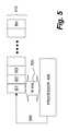
- FIG. 5is a block diagram of an image sensor architecture showing a bank switching scheme for matching memory data bus width to disparate data buses according to the invention.
- the memory 410is organized into a plurality of banks B 1 -B b , each bank having a specific width.
- the banksmay be accessed sequentially by the processor 320 , such that the bus width is equivalent to the bank width of a single bank.
- a narrower data bus 520is provided for use in conjunction with the processor 320 .
- the two or more of the banksmay be accessed simultaneously, such that the bus width is equivalent to the combined bank widths of all of the accessed banks.
- a wider data bus 502is provided for use in conjunction with the image sensor 302 .
- a simple switching means, operating under processor control 500reconfigures the memory on the fly.
- the inventionmay be implemented in schemes other than the bank switching scheme, such as a plane select scheme, the use of shift register, or other schemes as will be appreciated by those skilled in the art.
- the inventionneed not match narrow and wide buses, but may also be provided to match buses having different speeds or operating voltages as well.
- the inventionmay also use an external control to configure the bus width, for example to match the output of the device to various external systems or to implement various processor features, such as image cropping and the like.
- the processormay also select bus width to operate multiple internal and/or external devices simultaneously from the same memory.
- the various banksmay be assigned to two or more functional elements of the sensor architecture.
- the memory structure described hereinmay also be used in a serial fashion, such that data may be written by the image sensor through a first port and simultaneously read and/or written by the processor through a second port, thereby increasing the speed of operation. Accordingly, the scope of the present invention is defined by the appended claims rather than the forgoing description of embodiments.
Landscapes
- Engineering & Computer Science (AREA)
- Multimedia (AREA)
- Signal Processing (AREA)
- Human Computer Interaction (AREA)
- Transforming Light Signals Into Electric Signals (AREA)
Abstract
Description
Claims (18)
Priority Applications (1)
| Application Number | Priority Date | Filing Date | Title |
|---|---|---|---|
| US09/864,296US6791611B2 (en) | 2000-05-09 | 2001-05-23 | Dual ported memory for digital image sensor |
Applications Claiming Priority (3)
| Application Number | Priority Date | Filing Date | Title |
|---|---|---|---|
| US56763800A | 2000-05-09 | 2000-05-09 | |
| US09/567,786US6975355B1 (en) | 2000-02-22 | 2000-05-09 | Multiple sampling via a time-indexed method to achieve wide dynamic ranges |
| US09/864,296US6791611B2 (en) | 2000-05-09 | 2001-05-23 | Dual ported memory for digital image sensor |
Related Parent Applications (1)
| Application Number | Title | Priority Date | Filing Date |
|---|---|---|---|
| US09/567,786Continuation-In-PartUS6975355B1 (en) | 1999-07-30 | 2000-05-09 | Multiple sampling via a time-indexed method to achieve wide dynamic ranges |
Publications (2)
| Publication Number | Publication Date |
|---|---|
| US20010040633A1 US20010040633A1 (en) | 2001-11-15 |
| US6791611B2true US6791611B2 (en) | 2004-09-14 |
Family
ID=46257759
Family Applications (1)
| Application Number | Title | Priority Date | Filing Date |
|---|---|---|---|
| US09/864,296Expired - LifetimeUS6791611B2 (en) | 2000-05-09 | 2001-05-23 | Dual ported memory for digital image sensor |
Country Status (1)
| Country | Link |
|---|---|
| US (1) | US6791611B2 (en) |
Cited By (31)
| Publication number | Priority date | Publication date | Assignee | Title |
|---|---|---|---|---|
| US20030133621A1 (en)* | 2001-07-30 | 2003-07-17 | Koji Fujii | Parallel processing logic circuit for sensor signal processing |
| US20060064477A1 (en)* | 2004-09-23 | 2006-03-23 | Renkis Martin A | Mesh networked video and sensor surveillance system and method for wireless mesh networked sensors |
| US20060066721A1 (en)* | 2004-09-25 | 2006-03-30 | Martin Renkis | Wireless video surveillance system and method with dual encoding |
| US20060070107A1 (en)* | 2004-09-24 | 2006-03-30 | Martin Renkis | Wireless video surveillance system and method with remote viewing |
| US20060066720A1 (en)* | 2004-09-24 | 2006-03-30 | Martin Renkis | Wireless video surveillance system and method with external removable recording |
| US20060070108A1 (en)* | 2004-09-30 | 2006-03-30 | Martin Renkis | Wireless video surveillance system & method with digital input recorder interface and setup |
| US20060066729A1 (en)* | 2004-09-24 | 2006-03-30 | Martin Renkis | Wireless video surveillance system and method with DVR-based querying |
| US20060070109A1 (en)* | 2004-09-30 | 2006-03-30 | Martin Renkis | Wireless video surveillance system & method with rapid installation |
| US20060072757A1 (en)* | 2004-09-24 | 2006-04-06 | Martin Renkis | Wireless video surveillance system and method with emergency video access |
| US20060075235A1 (en)* | 2004-09-30 | 2006-04-06 | Martin Renkis | Wireless video surveillance system and method with security key |
| US20060072013A1 (en)* | 2004-09-23 | 2006-04-06 | Martin Renkis | Wireless video surveillance system and method with two-way locking of input capture devices |
| US20060071779A1 (en)* | 2004-09-30 | 2006-04-06 | Martin Renkis | Wireless video surveillance system & method with input capture and data transmission prioritization and adjustment |
| US20060075065A1 (en)* | 2004-09-30 | 2006-04-06 | Renkis Martin A | Wireless video surveillance system and method with single click-select actions |
| US20060095539A1 (en)* | 2004-10-29 | 2006-05-04 | Martin Renkis | Wireless video surveillance system and method for mesh networking |
| US20060143672A1 (en)* | 2004-09-23 | 2006-06-29 | Martin Renkis | Wireless video surveillance processing negative motion |
| US20060170662A1 (en)* | 2004-12-07 | 2006-08-03 | Haruhisa Kurane | Image pickup device |
| US20060222302A1 (en)* | 2005-03-31 | 2006-10-05 | Frank Levinson | Power and communication interface for sensors using a single tethered fiber |
| US20060228998A1 (en)* | 2005-03-31 | 2006-10-12 | Finisar Corporation | Sensors with modular architecture |
| US20060250276A1 (en)* | 2005-03-31 | 2006-11-09 | Finisar Corporation | Systems and methods for collecting data with sensors |
| US20070009104A1 (en)* | 2004-09-23 | 2007-01-11 | Renkis Martin A | Wireless smart camera system and method |
| US20070064109A1 (en)* | 2004-09-23 | 2007-03-22 | Renkis Martin A | Wireless video surveillance system and method for self-configuring network |
| US20070075888A1 (en)* | 2005-09-30 | 2007-04-05 | Michael Kelly | Digital readout method and apparatus |
| US7595883B1 (en)* | 2002-09-16 | 2009-09-29 | The Board Of Trustees Of The Leland Stanford Junior University | Biological analysis arrangement and approach therefor |
| US7603087B1 (en) | 2005-08-12 | 2009-10-13 | Smartvue Corporation | Wireless video surveillance jamming and interface prevention |
| US20100276572A1 (en)* | 2005-06-02 | 2010-11-04 | Sony Corporation | Semiconductor image sensor module and method of manufacturing the same |
| US8605853B2 (en) | 2011-07-01 | 2013-12-10 | Massachusetts Institute Of Technology | Methods and apparatus for in-pixel filtering in focal plane arrays |
| US8648287B1 (en) | 2005-05-27 | 2014-02-11 | Rambus Inc. | Image sensor using single photon jots and processor to create pixels |
| US8692176B2 (en) | 2006-10-27 | 2014-04-08 | Michael Kelly | Focal plane array processing method and apparatus |
| US20140103190A1 (en)* | 2012-10-12 | 2014-04-17 | Samsung Electronics Co., Ltd. | Binary image sensor and image sensing method |
| US8842179B2 (en) | 2004-09-24 | 2014-09-23 | Smartvue Corporation | Video surveillance sharing system and method |
| US9679929B2 (en) | 2012-10-12 | 2017-06-13 | Samsung Electronics Co., Ltd. | Binary image sensors including quantum dots and unit pixels thereof |
Families Citing this family (13)
| Publication number | Priority date | Publication date | Assignee | Title |
|---|---|---|---|---|
| US6786420B1 (en) | 1997-07-15 | 2004-09-07 | Silverbrook Research Pty. Ltd. | Data distribution mechanism in the form of ink dots on cards |
| US6618117B2 (en) | 1997-07-12 | 2003-09-09 | Silverbrook Research Pty Ltd | Image sensing apparatus including a microcontroller |
| US7551201B2 (en) | 1997-07-15 | 2009-06-23 | Silverbrook Research Pty Ltd | Image capture and processing device for a print on demand digital camera system |
| US6879341B1 (en) | 1997-07-15 | 2005-04-12 | Silverbrook Research Pty Ltd | Digital camera system containing a VLIW vector processor |
| US6624848B1 (en) | 1997-07-15 | 2003-09-23 | Silverbrook Research Pty Ltd | Cascading image modification using multiple digital cameras incorporating image processing |
| US6690419B1 (en) | 1997-07-15 | 2004-02-10 | Silverbrook Research Pty Ltd | Utilising eye detection methods for image processing in a digital image camera |
| US7110024B1 (en) | 1997-07-15 | 2006-09-19 | Silverbrook Research Pty Ltd | Digital camera system having motion deblurring means |
| AUPP702098A0 (en) | 1998-11-09 | 1998-12-03 | Silverbrook Research Pty Ltd | Image creation method and apparatus (ART73) |
| AUPQ056099A0 (en) | 1999-05-25 | 1999-06-17 | Silverbrook Research Pty Ltd | A method and apparatus (pprint01) |
| US20030206236A1 (en)* | 2002-05-06 | 2003-11-06 | Agfa Corporation | CMOS digital image sensor system and method |
| US7376777B2 (en)* | 2005-09-23 | 2008-05-20 | Freescale Semiconductor, Inc. | Performing an N-bit write access to an M×N-bit-only peripheral |
| US9955099B2 (en) | 2016-06-21 | 2018-04-24 | Hand Held Products, Inc. | Minimum height CMOS image sensor |
| US11212468B2 (en)* | 2018-03-14 | 2021-12-28 | Sony Advanced Visual Sensing Ag | Event-based vision sensor with direct memory control |
Citations (4)
| Publication number | Priority date | Publication date | Assignee | Title |
|---|---|---|---|---|
| US5461425A (en)* | 1994-02-15 | 1995-10-24 | Stanford University | CMOS image sensor with pixel level A/D conversion |
| US5801657A (en)* | 1997-02-05 | 1998-09-01 | Stanford University | Serial analog-to-digital converter using successive comparisons |
| US6115066A (en)* | 1997-06-12 | 2000-09-05 | International Business Machines Corporation | Image sensor with direct digital correlated sampling |
| US6704046B2 (en)* | 2002-04-17 | 2004-03-09 | Motorola, Inc. | Digital pixel image sensor with independent color channel reference signals |
- 2001
- 2001-05-23USUS09/864,296patent/US6791611B2/ennot_activeExpired - Lifetime
Patent Citations (4)
| Publication number | Priority date | Publication date | Assignee | Title |
|---|---|---|---|---|
| US5461425A (en)* | 1994-02-15 | 1995-10-24 | Stanford University | CMOS image sensor with pixel level A/D conversion |
| US5801657A (en)* | 1997-02-05 | 1998-09-01 | Stanford University | Serial analog-to-digital converter using successive comparisons |
| US6115066A (en)* | 1997-06-12 | 2000-09-05 | International Business Machines Corporation | Image sensor with direct digital correlated sampling |
| US6704046B2 (en)* | 2002-04-17 | 2004-03-09 | Motorola, Inc. | Digital pixel image sensor with independent color channel reference signals |
Cited By (85)
| Publication number | Priority date | Publication date | Assignee | Title |
|---|---|---|---|---|
| US7394052B2 (en)* | 2001-07-30 | 2008-07-01 | Nippon Telegraph And Telephone Corporation | Parallel processing logic circuit for sensor signal processing |
| US20030133621A1 (en)* | 2001-07-30 | 2003-07-17 | Koji Fujii | Parallel processing logic circuit for sensor signal processing |
| US8709788B2 (en) | 2002-09-16 | 2014-04-29 | The Board Of Trustees Of The Leland Stanford Junior University | Biological analysis arrangement and approach therefor |
| US7595883B1 (en)* | 2002-09-16 | 2009-09-29 | The Board Of Trustees Of The Leland Stanford Junior University | Biological analysis arrangement and approach therefor |
| US20060064477A1 (en)* | 2004-09-23 | 2006-03-23 | Renkis Martin A | Mesh networked video and sensor surveillance system and method for wireless mesh networked sensors |
| US20070064109A1 (en)* | 2004-09-23 | 2007-03-22 | Renkis Martin A | Wireless video surveillance system and method for self-configuring network |
| US20070009104A1 (en)* | 2004-09-23 | 2007-01-11 | Renkis Martin A | Wireless smart camera system and method |
| US7821533B2 (en) | 2004-09-23 | 2010-10-26 | Smartvue Corporation | Wireless video surveillance system and method with two-way locking of input capture devices |
| US8752106B2 (en) | 2004-09-23 | 2014-06-10 | Smartvue Corporation | Mesh networked video and sensor surveillance system and method for wireless mesh networked sensors |
| US20060143672A1 (en)* | 2004-09-23 | 2006-06-29 | Martin Renkis | Wireless video surveillance processing negative motion |
| US20060072013A1 (en)* | 2004-09-23 | 2006-04-06 | Martin Renkis | Wireless video surveillance system and method with two-way locking of input capture devices |
| US8457314B2 (en) | 2004-09-23 | 2013-06-04 | Smartvue Corporation | Wireless video surveillance system and method for self-configuring network |
| US7719571B2 (en) | 2004-09-24 | 2010-05-18 | Smartvue Corporation | Wireless video surveillance system and method with DVR-based querying |
| US7954129B2 (en) | 2004-09-24 | 2011-05-31 | Smartvue Corporation | Wireless video surveillance system and method with remote viewing |
| US20060072757A1 (en)* | 2004-09-24 | 2006-04-06 | Martin Renkis | Wireless video surveillance system and method with emergency video access |
| US8842179B2 (en) | 2004-09-24 | 2014-09-23 | Smartvue Corporation | Video surveillance sharing system and method |
| US20060066729A1 (en)* | 2004-09-24 | 2006-03-30 | Martin Renkis | Wireless video surveillance system and method with DVR-based querying |
| US8208019B2 (en) | 2004-09-24 | 2012-06-26 | Martin Renkis | Wireless video surveillance system and method with external removable recording |
| US20060066720A1 (en)* | 2004-09-24 | 2006-03-30 | Martin Renkis | Wireless video surveillance system and method with external removable recording |
| US20060070107A1 (en)* | 2004-09-24 | 2006-03-30 | Martin Renkis | Wireless video surveillance system and method with remote viewing |
| US7719567B2 (en) | 2004-09-24 | 2010-05-18 | Smartvue Corporation | Wireless video surveillance system and method with emergency video access |
| US7508418B2 (en) | 2004-09-24 | 2009-03-24 | Smartvue Corporation | Wireless video surveillance system and method with DVR-based querying |
| US20090237504A1 (en)* | 2004-09-24 | 2009-09-24 | Renkis Martin A | Wireless video surveillance system and method with DVR-based querying |
| US7936370B2 (en) | 2004-09-25 | 2011-05-03 | Smartvue Corporation | Wireless video surveillance system and method with dual encoding |
| US20060066721A1 (en)* | 2004-09-25 | 2006-03-30 | Martin Renkis | Wireless video surveillance system and method with dual encoding |
| US20060071779A1 (en)* | 2004-09-30 | 2006-04-06 | Martin Renkis | Wireless video surveillance system & method with input capture and data transmission prioritization and adjustment |
| US20060075065A1 (en)* | 2004-09-30 | 2006-04-06 | Renkis Martin A | Wireless video surveillance system and method with single click-select actions |
| US8253796B2 (en) | 2004-09-30 | 2012-08-28 | Smartvue Corp. | Wireless video surveillance system and method with rapid installation |
| US9544547B2 (en) | 2004-09-30 | 2017-01-10 | Kip Smrt P1 Lp | Monitoring smart devices on a wireless mesh communication network |
| US9407877B2 (en) | 2004-09-30 | 2016-08-02 | Kip Smrt P1 Lp | Wireless video surveillance system and method with input capture and data transmission prioritization and adjustment |
| US20060070108A1 (en)* | 2004-09-30 | 2006-03-30 | Martin Renkis | Wireless video surveillance system & method with digital input recorder interface and setup |
| US8199195B2 (en) | 2004-09-30 | 2012-06-12 | Martin Renkis | Wireless video surveillance system and method with security key |
| US8610772B2 (en) | 2004-09-30 | 2013-12-17 | Smartvue Corporation | Wireless video surveillance system and method with input capture and data transmission prioritization and adjustment |
| US7728871B2 (en) | 2004-09-30 | 2010-06-01 | Smartvue Corporation | Wireless video surveillance system & method with input capture and data transmission prioritization and adjustment |
| US7784080B2 (en) | 2004-09-30 | 2010-08-24 | Smartvue Corporation | Wireless video surveillance system and method with single click-select actions |
| US20100220188A1 (en)* | 2004-09-30 | 2010-09-02 | Renkis Martin A | Wireless Video Surveillance System and Method with Input Capture and Data Transmission Prioritization and Adjustment |
| US20060070109A1 (en)* | 2004-09-30 | 2006-03-30 | Martin Renkis | Wireless video surveillance system & method with rapid installation |
| US20060075235A1 (en)* | 2004-09-30 | 2006-04-06 | Martin Renkis | Wireless video surveillance system and method with security key |
| US10769910B2 (en) | 2004-10-29 | 2020-09-08 | Sensormatic Electronics, LLC | Surveillance systems with camera coordination for detecting events |
| US20060095539A1 (en)* | 2004-10-29 | 2006-05-04 | Martin Renkis | Wireless video surveillance system and method for mesh networking |
| US12100277B2 (en) | 2004-10-29 | 2024-09-24 | Johnson Controls Tyco IP Holdings LLP | Wireless environmental data capture system and method for mesh networking |
| US11450188B2 (en) | 2004-10-29 | 2022-09-20 | Johnson Controls Tyco IP Holdings LLP | Wireless environmental data capture system and method for mesh networking |
| US11138847B2 (en) | 2004-10-29 | 2021-10-05 | Sensormatic Electronics, LLC | Wireless environmental data capture system and method for mesh networking |
| US10504347B1 (en) | 2004-10-29 | 2019-12-10 | Sensormatic Electronics, LLC | Wireless environmental data capture system and method for mesh networking |
| US10115279B2 (en) | 2004-10-29 | 2018-10-30 | Sensomatic Electronics, LLC | Surveillance monitoring systems and methods for remotely viewing data and controlling cameras |
| US20060170662A1 (en)* | 2004-12-07 | 2006-08-03 | Haruhisa Kurane | Image pickup device |
| US7643075B2 (en) | 2004-12-07 | 2010-01-05 | Seiko Epson Corporation | Image pickup device |
| US8154414B2 (en) | 2005-03-31 | 2012-04-10 | Finisar Corporation | Systems and methods for collecting data with sensors |
| US20060222302A1 (en)* | 2005-03-31 | 2006-10-05 | Frank Levinson | Power and communication interface for sensors using a single tethered fiber |
| US20060228998A1 (en)* | 2005-03-31 | 2006-10-12 | Finisar Corporation | Sensors with modular architecture |
| US20060250276A1 (en)* | 2005-03-31 | 2006-11-09 | Finisar Corporation | Systems and methods for collecting data with sensors |
| US7859071B2 (en) | 2005-03-31 | 2010-12-28 | Finisar Corporation | Power and communication interface for sensors using a single tethered fiber |
| US7599583B2 (en)* | 2005-03-31 | 2009-10-06 | Finisar Corporation | Sensors with modular architecture |
| US9225918B1 (en) | 2005-05-27 | 2015-12-29 | Rambus Inc. | Image sensor having sub-diffraction-limit pixels |
| US8648287B1 (en) | 2005-05-27 | 2014-02-11 | Rambus Inc. | Image sensor using single photon jots and processor to create pixels |
| US11128831B1 (en) | 2005-05-27 | 2021-09-21 | Rambus Inc. | Image sensor having sub-diffraction-limit pixels |
| US10674098B1 (en) | 2005-05-27 | 2020-06-02 | Rambus Inc. | Image sensor having sub-diffraction-limit pixels |
| US9565385B1 (en) | 2005-05-27 | 2017-02-07 | Rambus Inc. | Image sensor having sub-diffraction-limit pixels |
| US10645324B2 (en) | 2005-06-02 | 2020-05-05 | Sony Corporation | Semiconductor image sensor module and method of manufacturing the same |
| US10129497B2 (en) | 2005-06-02 | 2018-11-13 | Sony Corporation | Semiconductor image sensor module and method of manufacturing the same |
| US11722800B2 (en) | 2005-06-02 | 2023-08-08 | Sony Group Corporation | Semiconductor image sensor module and method of manufacturing the same |
| US11228728B2 (en) | 2005-06-02 | 2022-01-18 | Sony Group Corporation | Semiconductor image sensor module and method of manufacturing the same |
| US8946610B2 (en)* | 2005-06-02 | 2015-02-03 | Sony Corporation | Semiconductor image sensor module and method of manufacturing the same |
| US20100276572A1 (en)* | 2005-06-02 | 2010-11-04 | Sony Corporation | Semiconductor image sensor module and method of manufacturing the same |
| US10594972B2 (en) | 2005-06-02 | 2020-03-17 | Sony Corporation | Semiconductor image sensor module and method of manufacturing the same |
| US9955097B2 (en) | 2005-06-02 | 2018-04-24 | Sony Corporation | Semiconductor image sensor module and method of manufacturing the same |
| US20090315991A1 (en)* | 2005-08-12 | 2009-12-24 | Renkis Martin A | Wireless Video Surveillance Jamming and Interference Prevention |
| US20090275287A1 (en)* | 2005-08-12 | 2009-11-05 | Renkis Martin A | Wireless video surveillance jamming and interface prevention |
| US7925219B2 (en) | 2005-08-12 | 2011-04-12 | Smartvue Corporation | Wireless video surveillance jamming and interference prevention |
| US7603087B1 (en) | 2005-08-12 | 2009-10-13 | Smartvue Corporation | Wireless video surveillance jamming and interface prevention |
| US20070075888A1 (en)* | 2005-09-30 | 2007-04-05 | Michael Kelly | Digital readout method and apparatus |
| US8933832B2 (en) | 2005-09-30 | 2015-01-13 | The Massachusetts Institute Of Technology | Digital readout method and apparatus |
| US8179296B2 (en) | 2005-09-30 | 2012-05-15 | The Massachusetts Institute Of Technology | Digital readout method and apparatus |
| US9385738B2 (en) | 2005-09-30 | 2016-07-05 | Massachusetts Institute Of Technology | Digital readout method and apparatus |
| US9712771B2 (en) | 2005-09-30 | 2017-07-18 | Massachusetts Institute Of Technology | Digital readout method and apparatus |
| US10348993B2 (en) | 2005-09-30 | 2019-07-09 | Massachusetts Institute Of Technology | Digital readout method and apparatus |
| US9491389B2 (en) | 2006-10-27 | 2016-11-08 | Massachusetts Institute Of Technology | Focal plane array processing method and apparatus |
| US10362254B2 (en) | 2006-10-27 | 2019-07-23 | Massachusetts Institute Of Technology | Focal plane array processing method and apparatus |
| US10893226B2 (en) | 2006-10-27 | 2021-01-12 | Massachusetts Institute Of Technology | Focal plane array processing method and apparatus |
| US8692176B2 (en) | 2006-10-27 | 2014-04-08 | Michael Kelly | Focal plane array processing method and apparatus |
| US9159446B2 (en) | 2011-07-01 | 2015-10-13 | Massachusetts Institute Of Technology | Methods and apparatus for in-pixel filtering in focal plane arrays including apparatus and method for counting pulses representing an analog signal |
| US8605853B2 (en) | 2011-07-01 | 2013-12-10 | Massachusetts Institute Of Technology | Methods and apparatus for in-pixel filtering in focal plane arrays |
| US9768785B2 (en) | 2011-07-01 | 2017-09-19 | Massachusetts Institute Of Technology | Methods and apparatus for counting pulses representing an analog signal |
| US20140103190A1 (en)* | 2012-10-12 | 2014-04-17 | Samsung Electronics Co., Ltd. | Binary image sensor and image sensing method |
| US9679929B2 (en) | 2012-10-12 | 2017-06-13 | Samsung Electronics Co., Ltd. | Binary image sensors including quantum dots and unit pixels thereof |
Also Published As
| Publication number | Publication date |
|---|---|
| US20010040633A1 (en) | 2001-11-15 |
Similar Documents
| Publication | Publication Date | Title |
|---|---|---|
| US6791611B2 (en) | Dual ported memory for digital image sensor | |
| US6975355B1 (en) | Multiple sampling via a time-indexed method to achieve wide dynamic ranges | |
| US20010040632A1 (en) | Multiple sampling via a time-indexed method to achieve wide dynamic ranges | |
| CN1312776C (en) | CMOS sensor matrix with memory interface | |
| US6721008B2 (en) | Integrated CMOS active pixel digital camera | |
| US6778212B1 (en) | Digital image sensor with on -chip programmable logic | |
| US6498576B1 (en) | Selective analog-to-digital conversion for a digital pixel sensor | |
| US6922210B2 (en) | Memory updating for digital pixel sensors | |
| US6563540B2 (en) | Light sensor with increased dynamic range | |
| US6452152B1 (en) | Sense amplifier having a precision analog reference level for use with image sensors | |
| US20060146152A1 (en) | Image sensor with built-in ISP and dual camera system | |
| US6380880B1 (en) | Digital pixel sensor with integrated charge transfer amplifier | |
| KR100359770B1 (en) | Active pixel circuit in CMOS image sensor | |
| WO2017101864A1 (en) | Image sensor, control method, and electronic device | |
| US6593967B1 (en) | Electronic camera having dual clocked line memory | |
| KR20030036202A (en) | Dual-mode cmos integrated imager | |
| EP4131939A1 (en) | Solid-state imaging device, method for driving solid-state imaging device, and electronic apparatus | |
| KR102037283B1 (en) | Image sensor, image signal processor and electronic device including the same | |
| JP2003078819A (en) | Solid-state imaging device and method for sweeping out electric charge | |
| JP2000165751A (en) | Solid-state imaging device and electronic camera |
Legal Events
| Date | Code | Title | Description |
|---|---|---|---|
| AS | Assignment | Owner name:PIXIM, INC., CALIFORNIA Free format text:ASSIGNMENT OF ASSIGNORS INTEREST;ASSIGNOR:YANG, MR. DAVID XIAO DONG;REEL/FRAME:014897/0030 Effective date:20040710 | |
| STCF | Information on status: patent grant | Free format text:PATENTED CASE | |
| FEPP | Fee payment procedure | Free format text:PAT HOLDER CLAIMS SMALL ENTITY STATUS, ENTITY STATUS SET TO SMALL (ORIGINAL EVENT CODE: LTOS); ENTITY STATUS OF PATENT OWNER: LARGE ENTITY | |
| FPAY | Fee payment | Year of fee payment:4 | |
| AS | Assignment | Owner name:COMERICA BANK, A TEXAS BANKING ASSOCIATION, MICHIG Free format text:SECURITY AGREEMENT;ASSIGNOR:PIXIM, INC., A CALIFORNIA CORPORATION;REEL/FRAME:026064/0625 Effective date:20110325 | |
| FEPP | Fee payment procedure | Free format text:PAYOR NUMBER ASSIGNED (ORIGINAL EVENT CODE: ASPN); ENTITY STATUS OF PATENT OWNER: LARGE ENTITY | |
| FPAY | Fee payment | Year of fee payment:8 | |
| AS | Assignment | Owner name:PIXIM, INC., CALIFORNIA Free format text:RELEASE BY SECURED PARTY;ASSIGNOR:COMERICA BANK;REEL/FRAME:028958/0954 Effective date:20120911 | |
| FEPP | Fee payment procedure | Free format text:PAT HOLDER NO LONGER CLAIMS SMALL ENTITY STATUS, ENTITY STATUS SET TO UNDISCOUNTED (ORIGINAL EVENT CODE: STOL); ENTITY STATUS OF PATENT OWNER: LARGE ENTITY | |
| FPAY | Fee payment | Year of fee payment:12 |