US6791371B1 - Power-down activated by differential-input multiplier and comparator - Google Patents
Power-down activated by differential-input multiplier and comparatorDownload PDFInfo
- Publication number
- US6791371B1 US6791371B1US10/249,280US24928003AUS6791371B1US 6791371 B1US6791371 B1US 6791371B1US 24928003 AUS24928003 AUS 24928003AUS 6791371 B1US6791371 B1US 6791371B1
- Authority
- US
- United States
- Prior art keywords
- differential
- transistor
- node
- current
- voltage
- Prior art date
- Legal status (The legal status is an assumption and is not a legal conclusion. Google has not performed a legal analysis and makes no representation as to the accuracy of the status listed.)
- Expired - Lifetime
Links
- 230000000295complement effectEffects0.000claimsabstractdescription40
- 230000003213activating effectEffects0.000claimsdescription6
- 239000000872bufferSubstances0.000claimsdescription5
- 238000001914filtrationMethods0.000claimsdescription5
- 239000003990capacitorSubstances0.000claimsdescription4
- 238000012935AveragingMethods0.000claims8
- 238000012358sourcingMethods0.000claims2
- 238000000034methodMethods0.000claims1
- 230000007423decreaseEffects0.000description4
- 238000010586diagramMethods0.000description2
- 230000004048modificationEffects0.000description2
- 238000012986modificationMethods0.000description2
- 230000035945sensitivityEffects0.000description2
- 238000006243chemical reactionMethods0.000description1
- 238000001514detection methodMethods0.000description1
- 239000000835fiberSubstances0.000description1
- 230000036039immunityEffects0.000description1
- 230000003287optical effectEffects0.000description1
- 230000003071parasitic effectEffects0.000description1
- -1resistorsSubstances0.000description1
- 239000004065semiconductorSubstances0.000description1
- 230000011664signalingEffects0.000description1
- 238000004088simulationMethods0.000description1
Images


Classifications
- H—ELECTRICITY
- H03—ELECTRONIC CIRCUITRY
- H03K—PULSE TECHNIQUE
- H03K5/00—Manipulating of pulses not covered by one of the other main groups of this subclass
- H03K5/19—Monitoring patterns of pulse trains
- H—ELECTRICITY
- H03—ELECTRONIC CIRCUITRY
- H03K—PULSE TECHNIQUE
- H03K5/00—Manipulating of pulses not covered by one of the other main groups of this subclass
- H03K5/22—Circuits having more than one input and one output for comparing pulses or pulse trains with each other according to input signal characteristics, e.g. slope, integral
- H03K5/24—Circuits having more than one input and one output for comparing pulses or pulse trains with each other according to input signal characteristics, e.g. slope, integral the characteristic being amplitude
- H03K5/2472—Circuits having more than one input and one output for comparing pulses or pulse trains with each other according to input signal characteristics, e.g. slope, integral the characteristic being amplitude using field effect transistors
- H03K5/2481—Circuits having more than one input and one output for comparing pulses or pulse trains with each other according to input signal characteristics, e.g. slope, integral the characteristic being amplitude using field effect transistors with at least one differential stage
Definitions
- This inventionrelates to electronic systems, and more particularly to powering down when equal voltages are detected on differential inputs.
- a pair of differential signalshas one signal line driven high when the other signal line is driven low to transmit a bit of data.
- the difference in voltage between the two signal lines in the differential pairrather than the absolute voltages, determines the data state.
- Fail-safe circuitsare sometimes added to differential inputs to detect when such a cable break occurs.
- a load resistor at the receiver side of a cableconnects the two signal lines in the differential pair. When the cable is disconnected, the load resistor equalizes the voltages on the two signal lines until both signal-line inputs to the differential receiver have the same voltage. This same-voltage condition is detected by the differential receiver, and the output of the differential receiver is forced to a known state, rather than left in an unstable or undefined state.
- FIG. 1is a block diagram of an equal-voltage detector for a differential input.
- FIG. 2is a schematic of a first part of a differential equal-voltage detector.
- FIG. 3is a schematic of a complementary part of a differential equal-voltage detector.
- FIG. 4is a waveform of operation of the equal-voltage power-down detector of FIGS. 2 - 3 .
- the present inventionrelates to an improvement in differential detectors.
- the following descriptionis presented to enable one of ordinary skill in the art to make and use the invention as provided in the context of a particular application and its requirements.
- Various modifications to the preferred embodimentwill be apparent to those with skill in the art, and the general principles defined herein may be applied to other embodiments. Therefore, the present invention is not intended to be limited to the particular embodiments shown and described, but is to be accorded the widest scope consistent with the principles and novel features herein disclosed.
- FIG. 1is a block diagram of an equal-voltage detector for a differential input.
- the voltages on a pair of differential inputsare normally different, except for a brief moment at cross-over during switching. When the voltages are equal, a failure is usually the cause, such as when a cable carrying the differential pair is disconnected or broken.
- Differential inputs VIN+, VIN ⁇are normally driven to opposite states by a differential transmitter (not shown).
- a load resistor (not shown) between VIN+ and VIN ⁇equalizes the two voltages when the transmitter no longer drives the differential inputs, such as when the transmitter is disconnected due to a cable break.
- Differential inputs VIN+, VIN ⁇are input to differential multiplier 10 , in both the normal and reverse connections (VIN+, VIN ⁇ , and VIN ⁇ , VIN+).
- the voltage difference (VIN+ ⁇ VIN ⁇ )is multiplied by the reverse voltage difference (VIN ⁇ VIN+) by differential multiplier 10 .
- the output of differential multiplier 10is A 2 .
- the averaged output of differential multiplier 10is A 2 /2.
- the output of differential multiplier 10is filtered by low-pass filter 14 to produce a smoothed or averaged voltage V 2 .
- This averaged voltage V 2can be the average over several cycles of the differential input at the target switching frequency.
- the averaged voltage V 2is applied to the non-inverting (+) input of differential comparator 16 .
- the inverting input ( ⁇ ) of differential comparator 16receives a reference voltage VREF.
- V 2is above VREF, differential comparator 16 outputs a high to inverter 18 , which drives power-down signal PD low (inactive).
- V 2When V 2 is below VREF, differential comparator 16 outputs a low to inverter 18 , which drives power-down signal PD high (active). Since V 2 is proportional to the square of the absolute voltage difference between differential inputs VIN+, VIN ⁇ , V 2 is a measure of the differential signal strength. When a failure occurs and VIN+, VIN ⁇ equalize, V 2 drops to zero.
- Reference voltage VREFcan be set to a predetermined value that is below V 2 during normal operation, but above V 2 when differential inputs VIN+, VIN ⁇ are equalized. The exact value of VREF used can be estimated or determined by circuit simulation, and a range of values may be substituted. Sensitivity of the power-down detector can be increased by lowering VREF, while false triggering can be reduced by increasing VREF.
- FIG. 2is a schematic of a first part of a differential equal-voltage detector.
- Differential inputs VIN+, VIN ⁇are applied to first differential multiplier 60 , which is a Gilbert multiplier.
- N-channel tail transistor 62receives a bias voltage BIASN on its gate, and sinks a constant current that is combined from the four legs of n-channel multiplier transistors 72 , 74 , 76 , 78 .
- P-channel current source transistors 68 , 70each have their gates and drains connected together. The gate and drain of p-channel source transistor 68 is node VQ 1 , while gate and drain of p-channel source transistor 70 is node VQ 2 . Nodes VQ 1 , VQ 2 are the outputs of first differential multiplier 60 .
- first filter comparator 80Differential-to-single-ended conversion is performed by first filter comparator 80 .
- the filtering and comparing functionsare combined. Filtering is provided by drain resistance of transistors 88 , 84 of first filter comparator 80 and the gate capacitances of transistors 92 , 94 of inverter 90 . Rather than explicitly compare the outputs of first differential multiplier 60 to a reference voltage VREF, the reference voltage is implicitly determined by the switching voltage of first filter comparator 80 and inverter 90 .
- the VQ 1 output of first differential multiplier 60is applied to the gate of p-channel transistor 88 , while the VQ 2 output of first differential multiplier 60 is applied to the gate of p-channel transistor 86 .
- Mirrored currentis provided to the drains of transistors 86 , 88 by n-channel mirror transistors 82 , 84 , respectively, which have their gates connected together and to the drain of n-channel mirror transistor 82 .
- the drains of n-channel mirror transistor 84 and p-channel transistor 88are the V 3 output of first filter comparator 60 .
- multiplier transistors 74 , 76which receive VIN+ at their gates, have a higher transconductance than multiplier transistors 72 , 78 , which receive VIN ⁇ at their gates. Multiplier transistors 72 , 78 tend to turn off when VIN ⁇ goes low.
- n-channel differential transistor 64changes in current through n-channel differential transistor 64 are coupled to p-channel current-source transistor 70 through multiplier transistor 74
- changes to current through n-channel differential transistor 66are coupled to p-channel current-source transistor 68 through multiplier transistor 76 .
- the lower VIN ⁇produces less current through transistor 64 .
- the lower current through transistor 64pulls less current from current-source transistor 70 , causing its gate and drain, node VQ 2 , to rise in voltage. This higher VQ 2 voltage decreases the current through p-channel transistor 86 .
- the reduced current sourced by transistor 86also reduces the current through n-channel transistor 82 , causing Its gate voltage to fall and reduce the current through n-channel transistor 84 . This reduces the pull-down current from node V 3 and thus helps raise the voltage of node V 3 , and inverter 90 drives PD low (inactive).
- multiplier transistors 74 , 76which receive VIN+ at their gates, have a lower transconductance than multiplier transistors 72 , 78 , which receive VIN ⁇ at their gates. Multiplier transistors 74 , 76 tend to turn off when VIN+ goes low.
- Changes in current through n-channel differential transistor 64are coupled to p-channel current-source transistor 68 through multiplier transistor 72
- changes in current through n-channel differential transistor 66are coupled to p-channel current-source transistor 70 through multiplier transistor 78 .
- the higher VIN ⁇causes more current to pass through differential transistor 64 than through differential transistor 66 .
- the increased current through transistor 64pulls more current from current-source transistor 68 , causing its gate and drain, node VQ 1 , to fall in voltage.
- This lower VQ 1 voltageincreases the current through p-channel transistor 88 .
- the higher current sourced by transistor 88raises the voltage of node V 3 , and inverter 90 drives PD low (inactive).
- the lower VIN+produces less current through transistor 66 .
- the lower current through transistor 66pulls less current from current-source transistor 70 , causing its gate and drain, node VQ 2 , to rise in voltage. This higher VQ 2 voltage decreases the current through p-channel transistor 86 .
- the reduced current sourced by transistor 86also reduces the current through n-channel transistor 82 , causing its gate voltage to fall and reduce the current through n-channel transistor 84 . This reduces the pull-down current from node V 3 and thus helps raise the voltage of node V 3 , and inverter 90 drives PD low (inactive).
- Transistor 86is larger than transistor 88 , so that when VQ 1 and VQ 2 are equal, more current is sourced by transistor 86 than transistor 88 .
- the larger current in transistor 86draws more current through n-channel transistor 82 , raising its gate voltage. This increases the pull-down current from node V 3 through n-channel transistor 84 , lowering V 3 . Since the voltage of VQ 1 is less when VIN+, VIN ⁇ have a differential voltage, and more when VIN+ and VIN ⁇ are equal, the higher VQ 1 reduces the source current through transistor 88 , allowing node V 3 to fall.
- the lower V 3is inverted by inverter 90 , driving power-down signal PD high, activating the power-down mode.
- FIG. 3is a schematic of a complementary part of a differential equal-voltage detector.
- Differential inputs VIN+, VIN ⁇are applied to second differential multiplier 20 , which is a Gilbert multiplier using complementary devices.
- the p-channel and n-channel transistorsare generally reversed compared with FIG. 2 . Operating principles are similar.
- first differential multiplier 60operates well when the common-mode voltage of VIN+, VIN ⁇ is above Vcc/2, performance can be degraded for voltages below Vcc/2.
- Second differential multiplier 20 and second filter comparator 40 having complementary devicesare added to operate when the common-mode input voltage is below Vcc/2.
- Bias generator 50generates bias voltage BIASP that is applied to the gate of p-channel tail transistor 22 , which supplies current to all legs of second differential multiplier 20 .
- Bias generator 50also generates BIASN for n-channel tail transistor 62 in second differential multiplier 60 of FIG. 2 .
- Bias generator 50is a voltage divider of p-channel transistor 52 , resistor 56 , and n-channel transistor 54 .
- the gate and drain of p-channel transistor 52generate bias BIASP, while gate and drain of n-channel transistor 55 generate bias BIASN.
- the current from p-channel tail transistor 22is split into two legs at the drain of transistor 22 .
- One current legpasses through p-channel differential transistor 24 , which has VIN ⁇ at its gate, while the other current leg passes through p-channel differential transistor 26 , which has VIN+ at its gate.
- VIN+, VIN ⁇are equal voltages, the same current passes through each leg.
- Non-equal VIN+, VIN ⁇produce a current difference in the two legs.
- the drain of p-channel differential transistor 24is connected to the sources of p-channel multiplier transistors 32 , 34 , which receive voltages VIN+, VIN ⁇ , respectively at their gates. This further splits current through transistor 24 into two legs.
- the drain of p-channel differential transistor 26is connected to the sources of p-channel multiplier transistors 36 , 38 , which receive voltages VIN ⁇ , VIN+, respectively at their gates. This further splits current through transistor 26 into two legs.
- the source current of tail transistor 22is thus split into a total of four current legs, through transistors 32 , 34 , 36 , 38 .
- multiplier transistors 32 , 36are combined since their drains are connected together. This combined current is sunk by n-channel current-sink transistor 28 , which has its gate and drain connected together as output node VM 1 from second differential multiplier 20 .
- This combined currentincludes one current through transistors 24 , 32 , and another current through transistors 26 , 36 .
- the gates of transistors 24 , 32are VIN ⁇ , VIN+, respectively, while gates of transistors 26 , 36 are VIN+, VIN ⁇ , respectively.
- the VM 1 output of second differential multiplier 20is applied to the gate of n-channel transistor 48
- the VM 2 output of second differential multiplier 20is applied to the gate of n-channel transistor 46
- Mirrored currentis provided to the drains of transistors 46 , 48 by p-channel mirror transistors 42 , 44 , respectively, which have their gates connected together and to the drain of p-channel mirror transistor 42 .
- the drains of p-channel mirror transistor 44 and n-channel transistor 48are the V 3 output of first filter comparator 40 .
- first filter comparator 80 and second filter comparator 40are combined at node V 3 .
- node V 3rises above a switching threshold, PD is driven low.
- multiplier transistors 34 , 36which receive VIN ⁇ at their gates, have a greater transconductance than multiplier transistors 32 , 38 , which receive VIN+ at their gates. Multiplier transistors 32 , 38 tend to turn off when VIN+ goes high.
- Changes in current through p-channel differential transistor 24are coupled to n-channel current-sink transistor 30 through multiplier transistor 34
- changes in current through p-channel differential transistor 26are coupled to n-channel current-sink transistor 28 through multiplier transistor 36 .
- the lower VIN ⁇causes more current to pass through p-channel differential transistor 24 than through differential transistor 26 .
- the increased current through transistor 24pulls more current from current-sink transistor 30 , causing its gate and drain, node VM 2 , to rise in voltage.
- This higher VM 2 voltageincreases the current through n-channel transistor 46 .
- the increased current sunk by transistor 46increases the current through p-channel transistor 42 , causing its gate voltage to fall and increase the current through p-channel transistor 44 . This increases the pull-up current from node V 3 and thus helps raise the voltage of node V 3 , and inverter 90 drives PD low (inactive).
- the higher VIN+produces less current through transistor 26 .
- the reduced current through transistor 26pulls less current from current-sink transistor 28 , causing its gate and drain, node VM 1 , to fall in voltage.
- This lower VM 1 voltagedecreases the current through n-channel transistor 48 .
- the lower current sourced by transistor 48raises the voltage of node V 3 , and inverter 90 drives PD low (inactive).
- multiplier transistors 34 , 36which receive VIN ⁇ at their gates, have a lower transconductance than multiplier transistors 32 , 38 , which receive VIN+ at their gates. Multiplier transistors 34 , 36 tend to turn off when VIN ⁇ goes high.
- Changes in current through p-channel differential transistor 24are coupled to n-channel current-sink transistor 28 through multiplier transistor 32
- changes in current through p-channel differential transistor 26are coupled to n-channel current-sink transistor 30 through multiplier transistor 38 .
- the lower VIN+causes more current to pass through differential transistor 26 than through differential transistor 24 .
- the increased current through transistor 26pulls more current from current-sink transistor 30 , causing its gate and drain, node VM 2 , to rise in voltage.
- This higher VM 2 voltageincreases the current through n-channel transistor 46 .
- the increased current sourced by transistor 46also increases the current through p-channel transistor 42 , causing its gate voltage to fall and increase the current through p-channel transistor 44 . This increases the pull-up current from node V 3 and thus helps raise the voltage of node V 3 , and inverter 90 drives PD low (inactive).
- the higher VIN ⁇produces less current through transistor 24 .
- the lower current through transistor 24pulls less current from current-sink transistor 28 , causing its gate and drain, node VM 1 , to fall in voltage.
- This lower VM 1 voltagedecreases the pull-down current thorough n-channel transistor 48 .
- the lower current sourced by transistor 48raises the voltage of node V 3 , and inverter 90 (FIG. 2) drives PD low (inactive).
- VIN+Since the voltage of VM 1 is less when VIN ⁇ , VIN+ have a differential voltage, and more when VIN ⁇ and VIN+ are equal, the higher VM 1 increases the current through transistor 48 , causing node V 3 to fall.
- the lower V 3is inverted by inverter 90 , driving power-down signal PD high, activating the power-down mode.
- Transistor 46is smaller than transistor 48 , so that when VM 1 and VM 2 are equal, more current is sunk by transistor 48 than transistor 46 .
- the smaller current in transistor 46reduces the current through p-channel transistor 42 , which is mirrored to reduce the pull-up current through p-channel transistor 44 .
- the reduced pull-up current from node V 3helps to pulls down node V 3 .
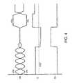
- FIG. 4is a waveform of operation of the equal-voltage power-down detector of FIGS. 2-3.
- VIN+, VIN ⁇operate normally, as shown by the initial series of sine wave inputs, the square voltage difference V 2 is above VREF.
- Power-down signal PDis low.
- the power-down signal PDis driven high to power-down the receiver or a sub-system or circuit that uses the differential receiver's output.
- V 2falls to zero. Since V 2 is still below VREF, power-down signal PD remains active.
- VIN+VIN ⁇ again diverge, as shown by the rectangular wave sequence at the right of the waveform, the large input-voltage difference causes V 2 to rise above VREF.
- the power-down signal PDis driven low to deactivate the power-down mode. Note that different voltage differences produce different values of V 2 that are still above VREF.
- First and second filter comparators 80 , 40may be combined so only one filter and comparator is needed.
- a voltage dividercould be added before the multiplier to limit the Vin+ and Vin ⁇ DC bias voltage of the multiplier from 0 to Vdd/2 (if the multiplier in FIG. 3 is used), or from Vdd/2 to Vdd (if the multiplier in FIG. 2 is used).
- either differential multiplier 20 or 60can work properly for input common mode voltage from 0 to Vdd.
Landscapes
- Physics & Mathematics (AREA)
- Nonlinear Science (AREA)
- Amplifiers (AREA)
Abstract
Description
Claims (20)
Priority Applications (1)
| Application Number | Priority Date | Filing Date | Title |
|---|---|---|---|
| US10/249,280US6791371B1 (en) | 2003-03-27 | 2003-03-27 | Power-down activated by differential-input multiplier and comparator |
Applications Claiming Priority (1)
| Application Number | Priority Date | Filing Date | Title |
|---|---|---|---|
| US10/249,280US6791371B1 (en) | 2003-03-27 | 2003-03-27 | Power-down activated by differential-input multiplier and comparator |
Publications (1)
| Publication Number | Publication Date |
|---|---|
| US6791371B1true US6791371B1 (en) | 2004-09-14 |
Family
ID=32926034
Family Applications (1)
| Application Number | Title | Priority Date | Filing Date |
|---|---|---|---|
| US10/249,280Expired - LifetimeUS6791371B1 (en) | 2003-03-27 | 2003-03-27 | Power-down activated by differential-input multiplier and comparator |
Country Status (1)
| Country | Link |
|---|---|
| US (1) | US6791371B1 (en) |
Cited By (9)
| Publication number | Priority date | Publication date | Assignee | Title |
|---|---|---|---|---|
| US20030174762A1 (en)* | 2002-03-14 | 2003-09-18 | Schoenborn Zale T. | Methods and apparatus for signaling on a differential link |
| US20030185308A1 (en)* | 2002-03-14 | 2003-10-02 | Schoenborn Zale T. | Methods and apparatus for reducing power usage of a transmitter and receiver coupled via a differential serial data link |
| US20040153611A1 (en)* | 2003-02-04 | 2004-08-05 | Sujat Jamil | Methods and apparatus for detecting an address conflict |
| US20050027945A1 (en)* | 2003-07-30 | 2005-02-03 | Desai Kiran R. | Methods and apparatus for maintaining cache coherency |
| US20050275435A1 (en)* | 2004-06-15 | 2005-12-15 | Kim Jung P | Comparator using differential amplifier with reduced current consumption |
| US20090067563A1 (en)* | 2007-09-12 | 2009-03-12 | National Taiwan University | Frequency synthesizer, coupled divide-by-n circuit, current-reuse multiply-by-m circuit |
| US20100127734A1 (en)* | 2008-11-25 | 2010-05-27 | Pericom Semiconductor Corp. | Out-Of-Band Signaling Using Detector with Equalizer, Multiplier and Comparator |
| US20150162654A1 (en)* | 2013-04-26 | 2015-06-11 | Panasonic Intellectual Property Management Co., Ltd. | Signal transmission device, signal transmission system, signal transmission method, and computer device |
| US20170093399A1 (en)* | 2015-09-30 | 2017-03-30 | Silicon Laboratories Inc. | High speed low current voltage comparator |
Citations (15)
| Publication number | Priority date | Publication date | Assignee | Title |
|---|---|---|---|---|
| US4408283A (en) | 1981-06-08 | 1983-10-04 | Transdata, Inc. | Time division multiplier transducer with digitally derived phase shift adjustment for reactive power and energy measurement |
| US4558283A (en) | 1983-02-18 | 1985-12-10 | Sony Corporation | Circuit for generating a sum or differential frequency signal |
| US4694204A (en) | 1984-02-29 | 1987-09-15 | Nec Corporation | Transistor circuit for signal multiplier |
| US4887071A (en) | 1988-08-18 | 1989-12-12 | Siemens Transmission Systems, Inc. | Digital activity loss detector |
| US5107150A (en) | 1990-05-31 | 1992-04-21 | Nec Corporation | Analog multiplier |
| US5561390A (en) | 1993-10-28 | 1996-10-01 | Nec Corporation | Clock signal generation circuit having detective circuit detecting loss of reference clock |
| US5574755A (en) | 1994-01-25 | 1996-11-12 | Philips Electronics North America Corporation | I/Q quadraphase modulator circuit |
| US5587687A (en) | 1995-02-02 | 1996-12-24 | Silicon Systems, Inc. | Multiplier based transconductance amplifiers and transconductance control circuits |
| US5754073A (en) | 1992-11-18 | 1998-05-19 | Nec Corporation | Analog multiplier |
| US5872446A (en) | 1997-08-12 | 1999-02-16 | International Business Machines Corporation | Low voltage CMOS analog multiplier with extended input dynamic range |
| US6020768A (en)* | 1998-05-13 | 2000-02-01 | Oak Technology, Inc. | CMOS low-voltage comparator |
| US6163172A (en) | 1998-04-06 | 2000-12-19 | Graychip, Inc. | Clock loss detector |
| US6201424B1 (en) | 1997-08-29 | 2001-03-13 | Micron Technology, Inc. | Synchronous clock generator including a delay-locked loop signal loss detector |
| US6222392B1 (en) | 1998-04-17 | 2001-04-24 | Advanced Micro Devices, Inc. | Signal monitoring circuit for detecting asynchronous clock loss |
| US6294932B1 (en)* | 1998-12-07 | 2001-09-25 | Nec Corporation | Input circuit, output circuit, input-output circuit and method of processing input signals |
- 2003
- 2003-03-27USUS10/249,280patent/US6791371B1/ennot_activeExpired - Lifetime
Patent Citations (15)
| Publication number | Priority date | Publication date | Assignee | Title |
|---|---|---|---|---|
| US4408283A (en) | 1981-06-08 | 1983-10-04 | Transdata, Inc. | Time division multiplier transducer with digitally derived phase shift adjustment for reactive power and energy measurement |
| US4558283A (en) | 1983-02-18 | 1985-12-10 | Sony Corporation | Circuit for generating a sum or differential frequency signal |
| US4694204A (en) | 1984-02-29 | 1987-09-15 | Nec Corporation | Transistor circuit for signal multiplier |
| US4887071A (en) | 1988-08-18 | 1989-12-12 | Siemens Transmission Systems, Inc. | Digital activity loss detector |
| US5107150A (en) | 1990-05-31 | 1992-04-21 | Nec Corporation | Analog multiplier |
| US5754073A (en) | 1992-11-18 | 1998-05-19 | Nec Corporation | Analog multiplier |
| US5561390A (en) | 1993-10-28 | 1996-10-01 | Nec Corporation | Clock signal generation circuit having detective circuit detecting loss of reference clock |
| US5574755A (en) | 1994-01-25 | 1996-11-12 | Philips Electronics North America Corporation | I/Q quadraphase modulator circuit |
| US5587687A (en) | 1995-02-02 | 1996-12-24 | Silicon Systems, Inc. | Multiplier based transconductance amplifiers and transconductance control circuits |
| US5872446A (en) | 1997-08-12 | 1999-02-16 | International Business Machines Corporation | Low voltage CMOS analog multiplier with extended input dynamic range |
| US6201424B1 (en) | 1997-08-29 | 2001-03-13 | Micron Technology, Inc. | Synchronous clock generator including a delay-locked loop signal loss detector |
| US6163172A (en) | 1998-04-06 | 2000-12-19 | Graychip, Inc. | Clock loss detector |
| US6222392B1 (en) | 1998-04-17 | 2001-04-24 | Advanced Micro Devices, Inc. | Signal monitoring circuit for detecting asynchronous clock loss |
| US6020768A (en)* | 1998-05-13 | 2000-02-01 | Oak Technology, Inc. | CMOS low-voltage comparator |
| US6294932B1 (en)* | 1998-12-07 | 2001-09-25 | Nec Corporation | Input circuit, output circuit, input-output circuit and method of processing input signals |
Cited By (26)
| Publication number | Priority date | Publication date | Assignee | Title |
|---|---|---|---|---|
| US7394863B2 (en) | 2002-03-14 | 2008-07-01 | Intel Corporation | Methods and apparatus for signaling on a differential link |
| US8885735B2 (en) | 2002-03-14 | 2014-11-11 | Intel Corporation | Methods and apparatus for signaling on a differential link |
| US9503289B2 (en) | 2002-03-14 | 2016-11-22 | Intel Corporation | Methods and apparatus for signaling on a differential link |
| US7496149B2 (en) | 2002-03-14 | 2009-02-24 | Intel Corporation | Methods and apparatus for signaling on a differential link |
| US8908807B2 (en) | 2002-03-14 | 2014-12-09 | Intel Corporation | Methods and apparatus for signaling on a differential link |
| US7170949B2 (en)* | 2002-03-14 | 2007-01-30 | Intel Corporation | Methods and apparatus for signaling on a differential link |
| US7200186B2 (en)* | 2002-03-14 | 2007-04-03 | Intel Corporation | Methods and apparatus for reducing power usage of a transmitter and receiver coupled via a differential serial data link |
| US20070081598A1 (en)* | 2002-03-14 | 2007-04-12 | Schoenborn Zale T | Methods and apparatus for signaling on a differential link |
| US20070086531A1 (en)* | 2002-03-14 | 2007-04-19 | Schoenborn Zale T | Methods and apparatus for signaling on a differential link |
| US20070116134A1 (en)* | 2002-03-14 | 2007-05-24 | Schoenborn Zale T | Methods and apparatus for reducing power usage of a transmitter and receiver coupled via a differential serial data link |
| US20030174762A1 (en)* | 2002-03-14 | 2003-09-18 | Schoenborn Zale T. | Methods and apparatus for signaling on a differential link |
| US20090122905A1 (en)* | 2002-03-14 | 2009-05-14 | Schoenborn Zale T | Methods and apparatus for signaling on a differential link |
| US20030185308A1 (en)* | 2002-03-14 | 2003-10-02 | Schoenborn Zale T. | Methods and apparatus for reducing power usage of a transmitter and receiver coupled via a differential serial data link |
| US20040153611A1 (en)* | 2003-02-04 | 2004-08-05 | Sujat Jamil | Methods and apparatus for detecting an address conflict |
| US7287126B2 (en) | 2003-07-30 | 2007-10-23 | Intel Corporation | Methods and apparatus for maintaining cache coherency |
| US20050027945A1 (en)* | 2003-07-30 | 2005-02-03 | Desai Kiran R. | Methods and apparatus for maintaining cache coherency |
| US20050275435A1 (en)* | 2004-06-15 | 2005-12-15 | Kim Jung P | Comparator using differential amplifier with reduced current consumption |
| US7298182B2 (en)* | 2004-06-15 | 2007-11-20 | Infineon Technologies Ag | Comparator using differential amplifier with reduced current consumption |
| US7671635B2 (en)* | 2007-09-12 | 2010-03-02 | National Taiwan University | Frequency synthesizer, coupled divide-by-N circuit, current-reuse multiply-by-M circuit |
| US20090067563A1 (en)* | 2007-09-12 | 2009-03-12 | National Taiwan University | Frequency synthesizer, coupled divide-by-n circuit, current-reuse multiply-by-m circuit |
| US20100127734A1 (en)* | 2008-11-25 | 2010-05-27 | Pericom Semiconductor Corp. | Out-Of-Band Signaling Using Detector with Equalizer, Multiplier and Comparator |
| US7808282B2 (en)* | 2008-11-25 | 2010-10-05 | Pericom Semiconductor Corp. | Out-of-band signaling using detector with equalizer, multiplier and comparator |
| US9093733B2 (en)* | 2013-04-26 | 2015-07-28 | Panasonic Intellectual Property Management Co., Ltd. | Signal transmission device, signal transmission system, signal transmission method, and computer device |
| US20150162654A1 (en)* | 2013-04-26 | 2015-06-11 | Panasonic Intellectual Property Management Co., Ltd. | Signal transmission device, signal transmission system, signal transmission method, and computer device |
| US20170093399A1 (en)* | 2015-09-30 | 2017-03-30 | Silicon Laboratories Inc. | High speed low current voltage comparator |
| US9866215B2 (en)* | 2015-09-30 | 2018-01-09 | Silicon Laboratories Inc. | High speed low current voltage comparator |
Similar Documents
| Publication | Publication Date | Title |
|---|---|---|
| US7224191B1 (en) | Differential signal detector methods and apparatus | |
| CN100547913C (en) | Fault secure differential receiver circuit and method thereof | |
| US6801059B2 (en) | Comparator with offset voltage | |
| US6791369B1 (en) | Clock presence detector comparing differential clock to common-mode voltage | |
| US7586336B2 (en) | Method and circuit for squelch detection in serial communications | |
| US5942921A (en) | Differential comparator with an extended input range | |
| US11228466B2 (en) | Digital capacitive isolator | |
| JP6133709B2 (en) | DIFFERENTIAL RECEIVER, ELECTRONIC DEVICE, INDUSTRIAL DEVICE USING THE DIFFERENTIAL RECEIVER, AND METHOD FOR RECEIVING DIFFERENTIAL SIGNAL | |
| US9735820B2 (en) | Multi-current harmonized paths for low power local interconnect network (LIN) receiver | |
| US6791371B1 (en) | Power-down activated by differential-input multiplier and comparator | |
| US8570072B2 (en) | Differential hysteresis comparator circuits and methods | |
| US6184701B1 (en) | Integrated circuit devices having metastability protection circuits therein | |
| US8884680B2 (en) | Signal electric potential conversion circuit | |
| JP3916502B2 (en) | Output circuit | |
| US7808282B2 (en) | Out-of-band signaling using detector with equalizer, multiplier and comparator | |
| JPH0559968U (en) | Integrated circuits and comparators | |
| US20030112058A1 (en) | Squelch circuit to create a squelch waveform for USB 2.0 | |
| US8138807B2 (en) | Power-on detecting circuit and level converting circuit | |
| US6642746B2 (en) | Phase detector with minimized phase detection error | |
| EP1550149B1 (en) | Constant delay zero standby differential logic receiver and method | |
| US7279909B1 (en) | Signal coincidence detection circuit | |
| US7164320B2 (en) | Current threshold circuit | |
| JP2930018B2 (en) | Voltage conversion circuit | |
| JPWO2005066733A1 (en) | Semiconductor device | |
| US7471108B2 (en) | Variable reference level input circuit and method |
Legal Events
| Date | Code | Title | Description |
|---|---|---|---|
| AS | Assignment | Owner name:PERICOM SEMICONDUCTOR CORP, CALIFORNIA Free format text:ASSIGNMENT OF ASSIGNORS INTEREST;ASSIGNOR:CHEUNG, HUNG-YAN;REEL/FRAME:013573/0301 Effective date:20030408 | |
| STCF | Information on status: patent grant | Free format text:PATENTED CASE | |
| FEPP | Fee payment procedure | Free format text:PAT HOLDER NO LONGER CLAIMS SMALL ENTITY STATUS, ENTITY STATUS SET TO UNDISCOUNTED (ORIGINAL EVENT CODE: STOL); ENTITY STATUS OF PATENT OWNER: LARGE ENTITY | |
| FPAY | Fee payment | Year of fee payment:4 | |
| FPAY | Fee payment | Year of fee payment:8 | |
| AS | Assignment | Owner name:BANK OF AMERICA, N.A., AS ADMINISTRATIVE AGENT, TE Free format text:SECURITY INTEREST;ASSIGNOR:PERICOM SEMICONDUCTOR CORPORATION, AS GRANTOR;REEL/FRAME:037255/0122 Effective date:20151209 | |
| FPAY | Fee payment | Year of fee payment:12 | |
| AS | Assignment | Owner name:DIODES INCORPORATED, TEXAS Free format text:ASSIGNMENT OF ASSIGNORS INTEREST;ASSIGNOR:PERICOM SEMICONDUCTOR CORPORATION;REEL/FRAME:044975/0554 Effective date:20171222 | |
| AS | Assignment | Owner name:BANK OF AMERICA, N.A., AS ADMIN. AGENT, NORTH CAROLINA Free format text:SECURITY AGREEMENT;ASSIGNOR:DIODES INCORPORATED;REEL/FRAME:045195/0446 Effective date:20180122 Owner name:BANK OF AMERICA, N.A., AS ADMIN. AGENT, NORTH CARO Free format text:SECURITY AGREEMENT;ASSIGNOR:DIODES INCORPORATED;REEL/FRAME:045195/0446 Effective date:20180122 |