US6791195B2 - Semiconductor device and manufacturing method of the same - Google Patents
Semiconductor device and manufacturing method of the sameDownload PDFInfo
- Publication number
- US6791195B2 US6791195B2US09/839,298US83929801AUS6791195B2US 6791195 B2US6791195 B2US 6791195B2US 83929801 AUS83929801 AUS 83929801AUS 6791195 B2US6791195 B2US 6791195B2
- Authority
- US
- United States
- Prior art keywords
- adhesive layer
- semiconductor
- semiconductor chip
- semiconductor device
- bump
- Prior art date
- Legal status (The legal status is an assumption and is not a legal conclusion. Google has not performed a legal analysis and makes no representation as to the accuracy of the status listed.)
- Expired - Lifetime, expires
Links
Images


Classifications
- H—ELECTRICITY
- H01—ELECTRIC ELEMENTS
- H01L—SEMICONDUCTOR DEVICES NOT COVERED BY CLASS H10
- H01L21/00—Processes or apparatus adapted for the manufacture or treatment of semiconductor or solid state devices or of parts thereof
- H01L21/67—Apparatus specially adapted for handling semiconductor or electric solid state devices during manufacture or treatment thereof; Apparatus specially adapted for handling wafers during manufacture or treatment of semiconductor or electric solid state devices or components ; Apparatus not specifically provided for elsewhere
- H01L21/683—Apparatus specially adapted for handling semiconductor or electric solid state devices during manufacture or treatment thereof; Apparatus specially adapted for handling wafers during manufacture or treatment of semiconductor or electric solid state devices or components ; Apparatus not specifically provided for elsewhere for supporting or gripping
- H01L21/6835—Apparatus specially adapted for handling semiconductor or electric solid state devices during manufacture or treatment thereof; Apparatus specially adapted for handling wafers during manufacture or treatment of semiconductor or electric solid state devices or components ; Apparatus not specifically provided for elsewhere for supporting or gripping using temporarily an auxiliary support
- H—ELECTRICITY
- H01—ELECTRIC ELEMENTS
- H01L—SEMICONDUCTOR DEVICES NOT COVERED BY CLASS H10
- H01L23/00—Details of semiconductor or other solid state devices
- H01L23/48—Arrangements for conducting electric current to or from the solid state body in operation, e.g. leads, terminal arrangements ; Selection of materials therefor
- H—ELECTRICITY
- H01—ELECTRIC ELEMENTS
- H01L—SEMICONDUCTOR DEVICES NOT COVERED BY CLASS H10
- H01L21/00—Processes or apparatus adapted for the manufacture or treatment of semiconductor or solid state devices or of parts thereof
- H01L21/02—Manufacture or treatment of semiconductor devices or of parts thereof
- H01L21/04—Manufacture or treatment of semiconductor devices or of parts thereof the devices having potential barriers, e.g. a PN junction, depletion layer or carrier concentration layer
- H01L21/50—Assembly of semiconductor devices using processes or apparatus not provided for in a single one of the groups H01L21/18 - H01L21/326 or H10D48/04 - H10D48/07 e.g. sealing of a cap to a base of a container
- H01L21/56—Encapsulations, e.g. encapsulation layers, coatings
- H01L21/563—Encapsulation of active face of flip-chip device, e.g. underfilling or underencapsulation of flip-chip, encapsulation preform on chip or mounting substrate
- H—ELECTRICITY
- H01—ELECTRIC ELEMENTS
- H01L—SEMICONDUCTOR DEVICES NOT COVERED BY CLASS H10
- H01L23/00—Details of semiconductor or other solid state devices
- H01L23/48—Arrangements for conducting electric current to or from the solid state body in operation, e.g. leads, terminal arrangements ; Selection of materials therefor
- H01L23/488—Arrangements for conducting electric current to or from the solid state body in operation, e.g. leads, terminal arrangements ; Selection of materials therefor consisting of soldered or bonded constructions
- H01L23/498—Leads, i.e. metallisations or lead-frames on insulating substrates, e.g. chip carriers
- H01L23/49811—Additional leads joined to the metallisation on the insulating substrate, e.g. pins, bumps, wires, flat leads
- H01L23/49816—Spherical bumps on the substrate for external connection, e.g. ball grid arrays [BGA]
- H—ELECTRICITY
- H01—ELECTRIC ELEMENTS
- H01L—SEMICONDUCTOR DEVICES NOT COVERED BY CLASS H10
- H01L24/00—Arrangements for connecting or disconnecting semiconductor or solid-state bodies; Methods or apparatus related thereto
- H01L24/01—Means for bonding being attached to, or being formed on, the surface to be connected, e.g. chip-to-package, die-attach, "first-level" interconnects; Manufacturing methods related thereto
- H01L24/26—Layer connectors, e.g. plate connectors, solder or adhesive layers; Manufacturing methods related thereto
- H01L24/28—Structure, shape, material or disposition of the layer connectors prior to the connecting process
- H01L24/29—Structure, shape, material or disposition of the layer connectors prior to the connecting process of an individual layer connector
- H—ELECTRICITY
- H01—ELECTRIC ELEMENTS
- H01L—SEMICONDUCTOR DEVICES NOT COVERED BY CLASS H10
- H01L25/00—Assemblies consisting of a plurality of semiconductor or other solid state devices
- H01L25/03—Assemblies consisting of a plurality of semiconductor or other solid state devices all the devices being of a type provided for in a single subclass of subclasses H10B, H10D, H10F, H10H, H10K or H10N, e.g. assemblies of rectifier diodes
- H01L25/04—Assemblies consisting of a plurality of semiconductor or other solid state devices all the devices being of a type provided for in a single subclass of subclasses H10B, H10D, H10F, H10H, H10K or H10N, e.g. assemblies of rectifier diodes the devices not having separate containers
- H01L25/065—Assemblies consisting of a plurality of semiconductor or other solid state devices all the devices being of a type provided for in a single subclass of subclasses H10B, H10D, H10F, H10H, H10K or H10N, e.g. assemblies of rectifier diodes the devices not having separate containers the devices being of a type provided for in group H10D89/00
- H01L25/0657—Stacked arrangements of devices
- H—ELECTRICITY
- H01—ELECTRIC ELEMENTS
- H01L—SEMICONDUCTOR DEVICES NOT COVERED BY CLASS H10
- H01L2221/00—Processes or apparatus adapted for the manufacture or treatment of semiconductor or solid state devices or of parts thereof covered by H01L21/00
- H01L2221/67—Apparatus for handling semiconductor or electric solid state devices during manufacture or treatment thereof; Apparatus for handling wafers during manufacture or treatment of semiconductor or electric solid state devices or components; Apparatus not specifically provided for elsewhere
- H01L2221/683—Apparatus for handling semiconductor or electric solid state devices during manufacture or treatment thereof; Apparatus for handling wafers during manufacture or treatment of semiconductor or electric solid state devices or components; Apparatus not specifically provided for elsewhere for supporting or gripping
- H01L2221/68304—Apparatus for handling semiconductor or electric solid state devices during manufacture or treatment thereof; Apparatus for handling wafers during manufacture or treatment of semiconductor or electric solid state devices or components; Apparatus not specifically provided for elsewhere for supporting or gripping using temporarily an auxiliary support
- H01L2221/68377—Apparatus for handling semiconductor or electric solid state devices during manufacture or treatment thereof; Apparatus for handling wafers during manufacture or treatment of semiconductor or electric solid state devices or components; Apparatus not specifically provided for elsewhere for supporting or gripping using temporarily an auxiliary support with parts of the auxiliary support remaining in the finished device
- H—ELECTRICITY
- H01—ELECTRIC ELEMENTS
- H01L—SEMICONDUCTOR DEVICES NOT COVERED BY CLASS H10
- H01L2224/00—Indexing scheme for arrangements for connecting or disconnecting semiconductor or solid-state bodies and methods related thereto as covered by H01L24/00
- H01L2224/01—Means for bonding being attached to, or being formed on, the surface to be connected, e.g. chip-to-package, die-attach, "first-level" interconnects; Manufacturing methods related thereto
- H01L2224/02—Bonding areas; Manufacturing methods related thereto
- H01L2224/04—Structure, shape, material or disposition of the bonding areas prior to the connecting process
- H01L2224/05—Structure, shape, material or disposition of the bonding areas prior to the connecting process of an individual bonding area
- H01L2224/0554—External layer
- H01L2224/0556—Disposition
- H01L2224/05571—Disposition the external layer being disposed in a recess of the surface
- H—ELECTRICITY
- H01—ELECTRIC ELEMENTS
- H01L—SEMICONDUCTOR DEVICES NOT COVERED BY CLASS H10
- H01L2224/00—Indexing scheme for arrangements for connecting or disconnecting semiconductor or solid-state bodies and methods related thereto as covered by H01L24/00
- H01L2224/01—Means for bonding being attached to, or being formed on, the surface to be connected, e.g. chip-to-package, die-attach, "first-level" interconnects; Manufacturing methods related thereto
- H01L2224/02—Bonding areas; Manufacturing methods related thereto
- H01L2224/04—Structure, shape, material or disposition of the bonding areas prior to the connecting process
- H01L2224/05—Structure, shape, material or disposition of the bonding areas prior to the connecting process of an individual bonding area
- H01L2224/0554—External layer
- H01L2224/05573—Single external layer
- H—ELECTRICITY
- H01—ELECTRIC ELEMENTS
- H01L—SEMICONDUCTOR DEVICES NOT COVERED BY CLASS H10
- H01L2224/00—Indexing scheme for arrangements for connecting or disconnecting semiconductor or solid-state bodies and methods related thereto as covered by H01L24/00
- H01L2224/01—Means for bonding being attached to, or being formed on, the surface to be connected, e.g. chip-to-package, die-attach, "first-level" interconnects; Manufacturing methods related thereto
- H01L2224/02—Bonding areas; Manufacturing methods related thereto
- H01L2224/04—Structure, shape, material or disposition of the bonding areas prior to the connecting process
- H01L2224/05—Structure, shape, material or disposition of the bonding areas prior to the connecting process of an individual bonding area
- H01L2224/0554—External layer
- H01L2224/05599—Material
- H01L2224/056—Material with a principal constituent of the material being a metal or a metalloid, e.g. boron [B], silicon [Si], germanium [Ge], arsenic [As], antimony [Sb], tellurium [Te] and polonium [Po], and alloys thereof
- H—ELECTRICITY
- H01—ELECTRIC ELEMENTS
- H01L—SEMICONDUCTOR DEVICES NOT COVERED BY CLASS H10
- H01L2224/00—Indexing scheme for arrangements for connecting or disconnecting semiconductor or solid-state bodies and methods related thereto as covered by H01L24/00
- H01L2224/01—Means for bonding being attached to, or being formed on, the surface to be connected, e.g. chip-to-package, die-attach, "first-level" interconnects; Manufacturing methods related thereto
- H01L2224/10—Bump connectors; Manufacturing methods related thereto
- H01L2224/11—Manufacturing methods
- H01L2224/113—Manufacturing methods by local deposition of the material of the bump connector
- H01L2224/1133—Manufacturing methods by local deposition of the material of the bump connector in solid form
- H01L2224/1134—Stud bumping, i.e. using a wire-bonding apparatus
- H—ELECTRICITY
- H01—ELECTRIC ELEMENTS
- H01L—SEMICONDUCTOR DEVICES NOT COVERED BY CLASS H10
- H01L2224/00—Indexing scheme for arrangements for connecting or disconnecting semiconductor or solid-state bodies and methods related thereto as covered by H01L24/00
- H01L2224/01—Means for bonding being attached to, or being formed on, the surface to be connected, e.g. chip-to-package, die-attach, "first-level" interconnects; Manufacturing methods related thereto
- H01L2224/10—Bump connectors; Manufacturing methods related thereto
- H01L2224/12—Structure, shape, material or disposition of the bump connectors prior to the connecting process
- H01L2224/13—Structure, shape, material or disposition of the bump connectors prior to the connecting process of an individual bump connector
- H01L2224/13001—Core members of the bump connector
- H01L2224/1302—Disposition
- H01L2224/13025—Disposition the bump connector being disposed on a via connection of the semiconductor or solid-state body
- H—ELECTRICITY
- H01—ELECTRIC ELEMENTS
- H01L—SEMICONDUCTOR DEVICES NOT COVERED BY CLASS H10
- H01L2224/00—Indexing scheme for arrangements for connecting or disconnecting semiconductor or solid-state bodies and methods related thereto as covered by H01L24/00
- H01L2224/01—Means for bonding being attached to, or being formed on, the surface to be connected, e.g. chip-to-package, die-attach, "first-level" interconnects; Manufacturing methods related thereto
- H01L2224/10—Bump connectors; Manufacturing methods related thereto
- H01L2224/12—Structure, shape, material or disposition of the bump connectors prior to the connecting process
- H01L2224/13—Structure, shape, material or disposition of the bump connectors prior to the connecting process of an individual bump connector
- H01L2224/13001—Core members of the bump connector
- H01L2224/13099—Material
- H01L2224/131—Material with a principal constituent of the material being a metal or a metalloid, e.g. boron [B], silicon [Si], germanium [Ge], arsenic [As], antimony [Sb], tellurium [Te] and polonium [Po], and alloys thereof
- H01L2224/13138—Material with a principal constituent of the material being a metal or a metalloid, e.g. boron [B], silicon [Si], germanium [Ge], arsenic [As], antimony [Sb], tellurium [Te] and polonium [Po], and alloys thereof the principal constituent melting at a temperature of greater than or equal to 950°C and less than 1550°C
- H01L2224/13144—Gold [Au] as principal constituent
- H—ELECTRICITY
- H01—ELECTRIC ELEMENTS
- H01L—SEMICONDUCTOR DEVICES NOT COVERED BY CLASS H10
- H01L2224/00—Indexing scheme for arrangements for connecting or disconnecting semiconductor or solid-state bodies and methods related thereto as covered by H01L24/00
- H01L2224/01—Means for bonding being attached to, or being formed on, the surface to be connected, e.g. chip-to-package, die-attach, "first-level" interconnects; Manufacturing methods related thereto
- H01L2224/10—Bump connectors; Manufacturing methods related thereto
- H01L2224/15—Structure, shape, material or disposition of the bump connectors after the connecting process
- H01L2224/16—Structure, shape, material or disposition of the bump connectors after the connecting process of an individual bump connector
- H01L2224/161—Disposition
- H01L2224/16135—Disposition the bump connector connecting between different semiconductor or solid-state bodies, i.e. chip-to-chip
- H01L2224/16145—Disposition the bump connector connecting between different semiconductor or solid-state bodies, i.e. chip-to-chip the bodies being stacked
- H—ELECTRICITY
- H01—ELECTRIC ELEMENTS
- H01L—SEMICONDUCTOR DEVICES NOT COVERED BY CLASS H10
- H01L2224/00—Indexing scheme for arrangements for connecting or disconnecting semiconductor or solid-state bodies and methods related thereto as covered by H01L24/00
- H01L2224/01—Means for bonding being attached to, or being formed on, the surface to be connected, e.g. chip-to-package, die-attach, "first-level" interconnects; Manufacturing methods related thereto
- H01L2224/10—Bump connectors; Manufacturing methods related thereto
- H01L2224/15—Structure, shape, material or disposition of the bump connectors after the connecting process
- H01L2224/16—Structure, shape, material or disposition of the bump connectors after the connecting process of an individual bump connector
- H01L2224/161—Disposition
- H01L2224/16151—Disposition the bump connector connecting between a semiconductor or solid-state body and an item not being a semiconductor or solid-state body, e.g. chip-to-substrate, chip-to-passive
- H01L2224/16221—Disposition the bump connector connecting between a semiconductor or solid-state body and an item not being a semiconductor or solid-state body, e.g. chip-to-substrate, chip-to-passive the body and the item being stacked
- H01L2224/16225—Disposition the bump connector connecting between a semiconductor or solid-state body and an item not being a semiconductor or solid-state body, e.g. chip-to-substrate, chip-to-passive the body and the item being stacked the item being non-metallic, e.g. insulating substrate with or without metallisation
- H—ELECTRICITY
- H01—ELECTRIC ELEMENTS
- H01L—SEMICONDUCTOR DEVICES NOT COVERED BY CLASS H10
- H01L2224/00—Indexing scheme for arrangements for connecting or disconnecting semiconductor or solid-state bodies and methods related thereto as covered by H01L24/00
- H01L2224/01—Means for bonding being attached to, or being formed on, the surface to be connected, e.g. chip-to-package, die-attach, "first-level" interconnects; Manufacturing methods related thereto
- H01L2224/26—Layer connectors, e.g. plate connectors, solder or adhesive layers; Manufacturing methods related thereto
- H01L2224/28—Structure, shape, material or disposition of the layer connectors prior to the connecting process
- H01L2224/29—Structure, shape, material or disposition of the layer connectors prior to the connecting process of an individual layer connector
- H01L2224/29001—Core members of the layer connector
- H01L2224/2901—Shape
- H01L2224/29011—Shape comprising apertures or cavities
- H—ELECTRICITY
- H01—ELECTRIC ELEMENTS
- H01L—SEMICONDUCTOR DEVICES NOT COVERED BY CLASS H10
- H01L2224/00—Indexing scheme for arrangements for connecting or disconnecting semiconductor or solid-state bodies and methods related thereto as covered by H01L24/00
- H01L2224/01—Means for bonding being attached to, or being formed on, the surface to be connected, e.g. chip-to-package, die-attach, "first-level" interconnects; Manufacturing methods related thereto
- H01L2224/26—Layer connectors, e.g. plate connectors, solder or adhesive layers; Manufacturing methods related thereto
- H01L2224/28—Structure, shape, material or disposition of the layer connectors prior to the connecting process
- H01L2224/29—Structure, shape, material or disposition of the layer connectors prior to the connecting process of an individual layer connector
- H01L2224/29001—Core members of the layer connector
- H01L2224/29099—Material
- H01L2224/291—Material with a principal constituent of the material being a metal or a metalloid, e.g. boron [B], silicon [Si], germanium [Ge], arsenic [As], antimony [Sb], tellurium [Te] and polonium [Po], and alloys thereof
- H01L2224/29101—Material with a principal constituent of the material being a metal or a metalloid, e.g. boron [B], silicon [Si], germanium [Ge], arsenic [As], antimony [Sb], tellurium [Te] and polonium [Po], and alloys thereof the principal constituent melting at a temperature of less than 400°C
- H01L2224/29111—Tin [Sn] as principal constituent
- H—ELECTRICITY
- H01—ELECTRIC ELEMENTS
- H01L—SEMICONDUCTOR DEVICES NOT COVERED BY CLASS H10
- H01L2224/00—Indexing scheme for arrangements for connecting or disconnecting semiconductor or solid-state bodies and methods related thereto as covered by H01L24/00
- H01L2224/01—Means for bonding being attached to, or being formed on, the surface to be connected, e.g. chip-to-package, die-attach, "first-level" interconnects; Manufacturing methods related thereto
- H01L2224/26—Layer connectors, e.g. plate connectors, solder or adhesive layers; Manufacturing methods related thereto
- H01L2224/28—Structure, shape, material or disposition of the layer connectors prior to the connecting process
- H01L2224/29—Structure, shape, material or disposition of the layer connectors prior to the connecting process of an individual layer connector
- H01L2224/29001—Core members of the layer connector
- H01L2224/29099—Material
- H01L2224/2919—Material with a principal constituent of the material being a polymer, e.g. polyester, phenolic based polymer, epoxy
- H—ELECTRICITY
- H01—ELECTRIC ELEMENTS
- H01L—SEMICONDUCTOR DEVICES NOT COVERED BY CLASS H10
- H01L2224/00—Indexing scheme for arrangements for connecting or disconnecting semiconductor or solid-state bodies and methods related thereto as covered by H01L24/00
- H01L2224/01—Means for bonding being attached to, or being formed on, the surface to be connected, e.g. chip-to-package, die-attach, "first-level" interconnects; Manufacturing methods related thereto
- H01L2224/26—Layer connectors, e.g. plate connectors, solder or adhesive layers; Manufacturing methods related thereto
- H01L2224/31—Structure, shape, material or disposition of the layer connectors after the connecting process
- H01L2224/32—Structure, shape, material or disposition of the layer connectors after the connecting process of an individual layer connector
- H01L2224/321—Disposition
- H01L2224/32135—Disposition the layer connector connecting between different semiconductor or solid-state bodies, i.e. chip-to-chip
- H01L2224/32145—Disposition the layer connector connecting between different semiconductor or solid-state bodies, i.e. chip-to-chip the bodies being stacked
- H—ELECTRICITY
- H01—ELECTRIC ELEMENTS
- H01L—SEMICONDUCTOR DEVICES NOT COVERED BY CLASS H10
- H01L2224/00—Indexing scheme for arrangements for connecting or disconnecting semiconductor or solid-state bodies and methods related thereto as covered by H01L24/00
- H01L2224/01—Means for bonding being attached to, or being formed on, the surface to be connected, e.g. chip-to-package, die-attach, "first-level" interconnects; Manufacturing methods related thereto
- H01L2224/26—Layer connectors, e.g. plate connectors, solder or adhesive layers; Manufacturing methods related thereto
- H01L2224/31—Structure, shape, material or disposition of the layer connectors after the connecting process
- H01L2224/32—Structure, shape, material or disposition of the layer connectors after the connecting process of an individual layer connector
- H01L2224/321—Disposition
- H01L2224/32151—Disposition the layer connector connecting between a semiconductor or solid-state body and an item not being a semiconductor or solid-state body, e.g. chip-to-substrate, chip-to-passive
- H01L2224/32221—Disposition the layer connector connecting between a semiconductor or solid-state body and an item not being a semiconductor or solid-state body, e.g. chip-to-substrate, chip-to-passive the body and the item being stacked
- H01L2224/32225—Disposition the layer connector connecting between a semiconductor or solid-state body and an item not being a semiconductor or solid-state body, e.g. chip-to-substrate, chip-to-passive the body and the item being stacked the item being non-metallic, e.g. insulating substrate with or without metallisation
- H—ELECTRICITY
- H01—ELECTRIC ELEMENTS
- H01L—SEMICONDUCTOR DEVICES NOT COVERED BY CLASS H10
- H01L2224/00—Indexing scheme for arrangements for connecting or disconnecting semiconductor or solid-state bodies and methods related thereto as covered by H01L24/00
- H01L2224/01—Means for bonding being attached to, or being formed on, the surface to be connected, e.g. chip-to-package, die-attach, "first-level" interconnects; Manufacturing methods related thereto
- H01L2224/26—Layer connectors, e.g. plate connectors, solder or adhesive layers; Manufacturing methods related thereto
- H01L2224/31—Structure, shape, material or disposition of the layer connectors after the connecting process
- H01L2224/32—Structure, shape, material or disposition of the layer connectors after the connecting process of an individual layer connector
- H01L2224/321—Disposition
- H01L2224/32151—Disposition the layer connector connecting between a semiconductor or solid-state body and an item not being a semiconductor or solid-state body, e.g. chip-to-substrate, chip-to-passive
- H01L2224/32221—Disposition the layer connector connecting between a semiconductor or solid-state body and an item not being a semiconductor or solid-state body, e.g. chip-to-substrate, chip-to-passive the body and the item being stacked
- H01L2224/32245—Disposition the layer connector connecting between a semiconductor or solid-state body and an item not being a semiconductor or solid-state body, e.g. chip-to-substrate, chip-to-passive the body and the item being stacked the item being metallic
- H—ELECTRICITY
- H01—ELECTRIC ELEMENTS
- H01L—SEMICONDUCTOR DEVICES NOT COVERED BY CLASS H10
- H01L2224/00—Indexing scheme for arrangements for connecting or disconnecting semiconductor or solid-state bodies and methods related thereto as covered by H01L24/00
- H01L2224/01—Means for bonding being attached to, or being formed on, the surface to be connected, e.g. chip-to-package, die-attach, "first-level" interconnects; Manufacturing methods related thereto
- H01L2224/42—Wire connectors; Manufacturing methods related thereto
- H01L2224/44—Structure, shape, material or disposition of the wire connectors prior to the connecting process
- H01L2224/45—Structure, shape, material or disposition of the wire connectors prior to the connecting process of an individual wire connector
- H01L2224/45001—Core members of the connector
- H01L2224/45099—Material
- H01L2224/451—Material with a principal constituent of the material being a metal or a metalloid, e.g. boron (B), silicon (Si), germanium (Ge), arsenic (As), antimony (Sb), tellurium (Te) and polonium (Po), and alloys thereof
- H01L2224/45138—Material with a principal constituent of the material being a metal or a metalloid, e.g. boron (B), silicon (Si), germanium (Ge), arsenic (As), antimony (Sb), tellurium (Te) and polonium (Po), and alloys thereof the principal constituent melting at a temperature of greater than or equal to 950°C and less than 1550°C
- H01L2224/45144—Gold (Au) as principal constituent
- H—ELECTRICITY
- H01—ELECTRIC ELEMENTS
- H01L—SEMICONDUCTOR DEVICES NOT COVERED BY CLASS H10
- H01L2224/00—Indexing scheme for arrangements for connecting or disconnecting semiconductor or solid-state bodies and methods related thereto as covered by H01L24/00
- H01L2224/73—Means for bonding being of different types provided for in two or more of groups H01L2224/10, H01L2224/18, H01L2224/26, H01L2224/34, H01L2224/42, H01L2224/50, H01L2224/63, H01L2224/71
- H01L2224/731—Location prior to the connecting process
- H01L2224/73101—Location prior to the connecting process on the same surface
- H01L2224/73103—Bump and layer connectors
- H01L2224/73104—Bump and layer connectors the bump connector being embedded into the layer connector
- H—ELECTRICITY
- H01—ELECTRIC ELEMENTS
- H01L—SEMICONDUCTOR DEVICES NOT COVERED BY CLASS H10
- H01L2224/00—Indexing scheme for arrangements for connecting or disconnecting semiconductor or solid-state bodies and methods related thereto as covered by H01L24/00
- H01L2224/73—Means for bonding being of different types provided for in two or more of groups H01L2224/10, H01L2224/18, H01L2224/26, H01L2224/34, H01L2224/42, H01L2224/50, H01L2224/63, H01L2224/71
- H01L2224/732—Location after the connecting process
- H01L2224/73201—Location after the connecting process on the same surface
- H01L2224/73203—Bump and layer connectors
- H01L2224/73204—Bump and layer connectors the bump connector being embedded into the layer connector
- H—ELECTRICITY
- H01—ELECTRIC ELEMENTS
- H01L—SEMICONDUCTOR DEVICES NOT COVERED BY CLASS H10
- H01L2224/00—Indexing scheme for arrangements for connecting or disconnecting semiconductor or solid-state bodies and methods related thereto as covered by H01L24/00
- H01L2224/73—Means for bonding being of different types provided for in two or more of groups H01L2224/10, H01L2224/18, H01L2224/26, H01L2224/34, H01L2224/42, H01L2224/50, H01L2224/63, H01L2224/71
- H01L2224/732—Location after the connecting process
- H01L2224/73251—Location after the connecting process on different surfaces
- H01L2224/73253—Bump and layer connectors
- H—ELECTRICITY
- H01—ELECTRIC ELEMENTS
- H01L—SEMICONDUCTOR DEVICES NOT COVERED BY CLASS H10
- H01L2224/00—Indexing scheme for arrangements for connecting or disconnecting semiconductor or solid-state bodies and methods related thereto as covered by H01L24/00
- H01L2224/80—Methods for connecting semiconductor or other solid state bodies using means for bonding being attached to, or being formed on, the surface to be connected
- H01L2224/81—Methods for connecting semiconductor or other solid state bodies using means for bonding being attached to, or being formed on, the surface to be connected using a bump connector
- H01L2224/8119—Arrangement of the bump connectors prior to mounting
- H01L2224/81191—Arrangement of the bump connectors prior to mounting wherein the bump connectors are disposed only on the semiconductor or solid-state body
- H—ELECTRICITY
- H01—ELECTRIC ELEMENTS
- H01L—SEMICONDUCTOR DEVICES NOT COVERED BY CLASS H10
- H01L2224/00—Indexing scheme for arrangements for connecting or disconnecting semiconductor or solid-state bodies and methods related thereto as covered by H01L24/00
- H01L2224/80—Methods for connecting semiconductor or other solid state bodies using means for bonding being attached to, or being formed on, the surface to be connected
- H01L2224/83—Methods for connecting semiconductor or other solid state bodies using means for bonding being attached to, or being formed on, the surface to be connected using a layer connector
- H01L2224/831—Methods for connecting semiconductor or other solid state bodies using means for bonding being attached to, or being formed on, the surface to be connected using a layer connector the layer connector being supplied to the parts to be connected in the bonding apparatus
- H01L2224/83101—Methods for connecting semiconductor or other solid state bodies using means for bonding being attached to, or being formed on, the surface to be connected using a layer connector the layer connector being supplied to the parts to be connected in the bonding apparatus as prepeg comprising a layer connector, e.g. provided in an insulating plate member
- H—ELECTRICITY
- H01—ELECTRIC ELEMENTS
- H01L—SEMICONDUCTOR DEVICES NOT COVERED BY CLASS H10
- H01L2224/00—Indexing scheme for arrangements for connecting or disconnecting semiconductor or solid-state bodies and methods related thereto as covered by H01L24/00
- H01L2224/80—Methods for connecting semiconductor or other solid state bodies using means for bonding being attached to, or being formed on, the surface to be connected
- H01L2224/83—Methods for connecting semiconductor or other solid state bodies using means for bonding being attached to, or being formed on, the surface to be connected using a layer connector
- H01L2224/831—Methods for connecting semiconductor or other solid state bodies using means for bonding being attached to, or being formed on, the surface to be connected using a layer connector the layer connector being supplied to the parts to be connected in the bonding apparatus
- H01L2224/83102—Methods for connecting semiconductor or other solid state bodies using means for bonding being attached to, or being formed on, the surface to be connected using a layer connector the layer connector being supplied to the parts to be connected in the bonding apparatus using surface energy, e.g. capillary forces
- H—ELECTRICITY
- H01—ELECTRIC ELEMENTS
- H01L—SEMICONDUCTOR DEVICES NOT COVERED BY CLASS H10
- H01L2224/00—Indexing scheme for arrangements for connecting or disconnecting semiconductor or solid-state bodies and methods related thereto as covered by H01L24/00
- H01L2224/80—Methods for connecting semiconductor or other solid state bodies using means for bonding being attached to, or being formed on, the surface to be connected
- H01L2224/83—Methods for connecting semiconductor or other solid state bodies using means for bonding being attached to, or being formed on, the surface to be connected using a layer connector
- H01L2224/8319—Arrangement of the layer connectors prior to mounting
- H01L2224/83191—Arrangement of the layer connectors prior to mounting wherein the layer connectors are disposed only on the semiconductor or solid-state body
- H—ELECTRICITY
- H01—ELECTRIC ELEMENTS
- H01L—SEMICONDUCTOR DEVICES NOT COVERED BY CLASS H10
- H01L2224/00—Indexing scheme for arrangements for connecting or disconnecting semiconductor or solid-state bodies and methods related thereto as covered by H01L24/00
- H01L2224/91—Methods for connecting semiconductor or solid state bodies including different methods provided for in two or more of groups H01L2224/80 - H01L2224/90
- H01L2224/92—Specific sequence of method steps
- H01L2224/921—Connecting a surface with connectors of different types
- H01L2224/9212—Sequential connecting processes
- H01L2224/92122—Sequential connecting processes the first connecting process involving a bump connector
- H01L2224/92125—Sequential connecting processes the first connecting process involving a bump connector the second connecting process involving a layer connector
- H—ELECTRICITY
- H01—ELECTRIC ELEMENTS
- H01L—SEMICONDUCTOR DEVICES NOT COVERED BY CLASS H10
- H01L2225/00—Details relating to assemblies covered by the group H01L25/00 but not provided for in its subgroups
- H01L2225/03—All the devices being of a type provided for in the same main group of the same subclass of class H10, e.g. assemblies of rectifier diodes
- H01L2225/04—All the devices being of a type provided for in the same main group of the same subclass of class H10, e.g. assemblies of rectifier diodes the devices not having separate containers
- H01L2225/065—All the devices being of a type provided for in the same main group of the same subclass of class H10
- H01L2225/06503—Stacked arrangements of devices
- H01L2225/06513—Bump or bump-like direct electrical connections between devices, e.g. flip-chip connection, solder bumps
- H—ELECTRICITY
- H01—ELECTRIC ELEMENTS
- H01L—SEMICONDUCTOR DEVICES NOT COVERED BY CLASS H10
- H01L2225/00—Details relating to assemblies covered by the group H01L25/00 but not provided for in its subgroups
- H01L2225/03—All the devices being of a type provided for in the same main group of the same subclass of class H10, e.g. assemblies of rectifier diodes
- H01L2225/04—All the devices being of a type provided for in the same main group of the same subclass of class H10, e.g. assemblies of rectifier diodes the devices not having separate containers
- H01L2225/065—All the devices being of a type provided for in the same main group of the same subclass of class H10
- H01L2225/06503—Stacked arrangements of devices
- H01L2225/06517—Bump or bump-like direct electrical connections from device to substrate
- H—ELECTRICITY
- H01—ELECTRIC ELEMENTS
- H01L—SEMICONDUCTOR DEVICES NOT COVERED BY CLASS H10
- H01L2225/00—Details relating to assemblies covered by the group H01L25/00 but not provided for in its subgroups
- H01L2225/03—All the devices being of a type provided for in the same main group of the same subclass of class H10, e.g. assemblies of rectifier diodes
- H01L2225/04—All the devices being of a type provided for in the same main group of the same subclass of class H10, e.g. assemblies of rectifier diodes the devices not having separate containers
- H01L2225/065—All the devices being of a type provided for in the same main group of the same subclass of class H10
- H01L2225/06503—Stacked arrangements of devices
- H01L2225/06541—Conductive via connections through the device, e.g. vertical interconnects, through silicon via [TSV]
- H—ELECTRICITY
- H01—ELECTRIC ELEMENTS
- H01L—SEMICONDUCTOR DEVICES NOT COVERED BY CLASS H10
- H01L2225/00—Details relating to assemblies covered by the group H01L25/00 but not provided for in its subgroups
- H01L2225/03—All the devices being of a type provided for in the same main group of the same subclass of class H10, e.g. assemblies of rectifier diodes
- H01L2225/04—All the devices being of a type provided for in the same main group of the same subclass of class H10, e.g. assemblies of rectifier diodes the devices not having separate containers
- H01L2225/065—All the devices being of a type provided for in the same main group of the same subclass of class H10
- H01L2225/06503—Stacked arrangements of devices
- H01L2225/06555—Geometry of the stack, e.g. form of the devices, geometry to facilitate stacking
- H—ELECTRICITY
- H01—ELECTRIC ELEMENTS
- H01L—SEMICONDUCTOR DEVICES NOT COVERED BY CLASS H10
- H01L2225/00—Details relating to assemblies covered by the group H01L25/00 but not provided for in its subgroups
- H01L2225/03—All the devices being of a type provided for in the same main group of the same subclass of class H10, e.g. assemblies of rectifier diodes
- H01L2225/04—All the devices being of a type provided for in the same main group of the same subclass of class H10, e.g. assemblies of rectifier diodes the devices not having separate containers
- H01L2225/065—All the devices being of a type provided for in the same main group of the same subclass of class H10
- H01L2225/06503—Stacked arrangements of devices
- H01L2225/06572—Auxiliary carrier between devices, the carrier having an electrical connection structure
- H—ELECTRICITY
- H01—ELECTRIC ELEMENTS
- H01L—SEMICONDUCTOR DEVICES NOT COVERED BY CLASS H10
- H01L2225/00—Details relating to assemblies covered by the group H01L25/00 but not provided for in its subgroups
- H01L2225/03—All the devices being of a type provided for in the same main group of the same subclass of class H10, e.g. assemblies of rectifier diodes
- H01L2225/04—All the devices being of a type provided for in the same main group of the same subclass of class H10, e.g. assemblies of rectifier diodes the devices not having separate containers
- H01L2225/065—All the devices being of a type provided for in the same main group of the same subclass of class H10
- H01L2225/06503—Stacked arrangements of devices
- H01L2225/06582—Housing for the assembly, e.g. chip scale package [CSP]
- H01L2225/06586—Housing with external bump or bump-like connectors
- H—ELECTRICITY
- H01—ELECTRIC ELEMENTS
- H01L—SEMICONDUCTOR DEVICES NOT COVERED BY CLASS H10
- H01L2225/00—Details relating to assemblies covered by the group H01L25/00 but not provided for in its subgroups
- H01L2225/03—All the devices being of a type provided for in the same main group of the same subclass of class H10, e.g. assemblies of rectifier diodes
- H01L2225/04—All the devices being of a type provided for in the same main group of the same subclass of class H10, e.g. assemblies of rectifier diodes the devices not having separate containers
- H01L2225/065—All the devices being of a type provided for in the same main group of the same subclass of class H10
- H01L2225/06503—Stacked arrangements of devices
- H01L2225/06589—Thermal management, e.g. cooling
- H—ELECTRICITY
- H01—ELECTRIC ELEMENTS
- H01L—SEMICONDUCTOR DEVICES NOT COVERED BY CLASS H10
- H01L24/00—Arrangements for connecting or disconnecting semiconductor or solid-state bodies; Methods or apparatus related thereto
- H01L24/01—Means for bonding being attached to, or being formed on, the surface to be connected, e.g. chip-to-package, die-attach, "first-level" interconnects; Manufacturing methods related thereto
- H01L24/02—Bonding areas ; Manufacturing methods related thereto
- H01L24/04—Structure, shape, material or disposition of the bonding areas prior to the connecting process
- H01L24/05—Structure, shape, material or disposition of the bonding areas prior to the connecting process of an individual bonding area
- H—ELECTRICITY
- H01—ELECTRIC ELEMENTS
- H01L—SEMICONDUCTOR DEVICES NOT COVERED BY CLASS H10
- H01L2924/00—Indexing scheme for arrangements or methods for connecting or disconnecting semiconductor or solid-state bodies as covered by H01L24/00
- H01L2924/01—Chemical elements
- H01L2924/01004—Beryllium [Be]
- H—ELECTRICITY
- H01—ELECTRIC ELEMENTS
- H01L—SEMICONDUCTOR DEVICES NOT COVERED BY CLASS H10
- H01L2924/00—Indexing scheme for arrangements or methods for connecting or disconnecting semiconductor or solid-state bodies as covered by H01L24/00
- H01L2924/01—Chemical elements
- H01L2924/01005—Boron [B]
- H—ELECTRICITY
- H01—ELECTRIC ELEMENTS
- H01L—SEMICONDUCTOR DEVICES NOT COVERED BY CLASS H10
- H01L2924/00—Indexing scheme for arrangements or methods for connecting or disconnecting semiconductor or solid-state bodies as covered by H01L24/00
- H01L2924/01—Chemical elements
- H01L2924/01006—Carbon [C]
- H—ELECTRICITY
- H01—ELECTRIC ELEMENTS
- H01L—SEMICONDUCTOR DEVICES NOT COVERED BY CLASS H10
- H01L2924/00—Indexing scheme for arrangements or methods for connecting or disconnecting semiconductor or solid-state bodies as covered by H01L24/00
- H01L2924/01—Chemical elements
- H01L2924/01013—Aluminum [Al]
- H—ELECTRICITY
- H01—ELECTRIC ELEMENTS
- H01L—SEMICONDUCTOR DEVICES NOT COVERED BY CLASS H10
- H01L2924/00—Indexing scheme for arrangements or methods for connecting or disconnecting semiconductor or solid-state bodies as covered by H01L24/00
- H01L2924/01—Chemical elements
- H01L2924/01015—Phosphorus [P]
- H—ELECTRICITY
- H01—ELECTRIC ELEMENTS
- H01L—SEMICONDUCTOR DEVICES NOT COVERED BY CLASS H10
- H01L2924/00—Indexing scheme for arrangements or methods for connecting or disconnecting semiconductor or solid-state bodies as covered by H01L24/00
- H01L2924/01—Chemical elements
- H01L2924/01023—Vanadium [V]
- H—ELECTRICITY
- H01—ELECTRIC ELEMENTS
- H01L—SEMICONDUCTOR DEVICES NOT COVERED BY CLASS H10
- H01L2924/00—Indexing scheme for arrangements or methods for connecting or disconnecting semiconductor or solid-state bodies as covered by H01L24/00
- H01L2924/01—Chemical elements
- H01L2924/01025—Manganese [Mn]
- H—ELECTRICITY
- H01—ELECTRIC ELEMENTS
- H01L—SEMICONDUCTOR DEVICES NOT COVERED BY CLASS H10
- H01L2924/00—Indexing scheme for arrangements or methods for connecting or disconnecting semiconductor or solid-state bodies as covered by H01L24/00
- H01L2924/01—Chemical elements
- H01L2924/01029—Copper [Cu]
- H—ELECTRICITY
- H01—ELECTRIC ELEMENTS
- H01L—SEMICONDUCTOR DEVICES NOT COVERED BY CLASS H10
- H01L2924/00—Indexing scheme for arrangements or methods for connecting or disconnecting semiconductor or solid-state bodies as covered by H01L24/00
- H01L2924/01—Chemical elements
- H01L2924/01033—Arsenic [As]
- H—ELECTRICITY
- H01—ELECTRIC ELEMENTS
- H01L—SEMICONDUCTOR DEVICES NOT COVERED BY CLASS H10
- H01L2924/00—Indexing scheme for arrangements or methods for connecting or disconnecting semiconductor or solid-state bodies as covered by H01L24/00
- H01L2924/01—Chemical elements
- H01L2924/01039—Yttrium [Y]
- H—ELECTRICITY
- H01—ELECTRIC ELEMENTS
- H01L—SEMICONDUCTOR DEVICES NOT COVERED BY CLASS H10
- H01L2924/00—Indexing scheme for arrangements or methods for connecting or disconnecting semiconductor or solid-state bodies as covered by H01L24/00
- H01L2924/01—Chemical elements
- H01L2924/0105—Tin [Sn]
- H—ELECTRICITY
- H01—ELECTRIC ELEMENTS
- H01L—SEMICONDUCTOR DEVICES NOT COVERED BY CLASS H10
- H01L2924/00—Indexing scheme for arrangements or methods for connecting or disconnecting semiconductor or solid-state bodies as covered by H01L24/00
- H01L2924/01—Chemical elements
- H01L2924/01078—Platinum [Pt]
- H—ELECTRICITY
- H01—ELECTRIC ELEMENTS
- H01L—SEMICONDUCTOR DEVICES NOT COVERED BY CLASS H10
- H01L2924/00—Indexing scheme for arrangements or methods for connecting or disconnecting semiconductor or solid-state bodies as covered by H01L24/00
- H01L2924/01—Chemical elements
- H01L2924/01079—Gold [Au]
- H—ELECTRICITY
- H01—ELECTRIC ELEMENTS
- H01L—SEMICONDUCTOR DEVICES NOT COVERED BY CLASS H10
- H01L2924/00—Indexing scheme for arrangements or methods for connecting or disconnecting semiconductor or solid-state bodies as covered by H01L24/00
- H01L2924/01—Chemical elements
- H01L2924/01082—Lead [Pb]
- H—ELECTRICITY
- H01—ELECTRIC ELEMENTS
- H01L—SEMICONDUCTOR DEVICES NOT COVERED BY CLASS H10
- H01L2924/00—Indexing scheme for arrangements or methods for connecting or disconnecting semiconductor or solid-state bodies as covered by H01L24/00
- H01L2924/013—Alloys
- H01L2924/0132—Binary Alloys
- H—ELECTRICITY
- H01—ELECTRIC ELEMENTS
- H01L—SEMICONDUCTOR DEVICES NOT COVERED BY CLASS H10
- H01L2924/00—Indexing scheme for arrangements or methods for connecting or disconnecting semiconductor or solid-state bodies as covered by H01L24/00
- H01L2924/15—Details of package parts other than the semiconductor or other solid state devices to be connected
- H01L2924/151—Die mounting substrate
- H01L2924/1515—Shape
- H01L2924/15151—Shape the die mounting substrate comprising an aperture, e.g. for underfilling, outgassing, window type wire connections
- H—ELECTRICITY
- H01—ELECTRIC ELEMENTS
- H01L—SEMICONDUCTOR DEVICES NOT COVERED BY CLASS H10
- H01L2924/00—Indexing scheme for arrangements or methods for connecting or disconnecting semiconductor or solid-state bodies as covered by H01L24/00
- H01L2924/15—Details of package parts other than the semiconductor or other solid state devices to be connected
- H01L2924/151—Die mounting substrate
- H01L2924/1515—Shape
- H01L2924/15153—Shape the die mounting substrate comprising a recess for hosting the device
- H—ELECTRICITY
- H01—ELECTRIC ELEMENTS
- H01L—SEMICONDUCTOR DEVICES NOT COVERED BY CLASS H10
- H01L2924/00—Indexing scheme for arrangements or methods for connecting or disconnecting semiconductor or solid-state bodies as covered by H01L24/00
- H01L2924/15—Details of package parts other than the semiconductor or other solid state devices to be connected
- H01L2924/151—Die mounting substrate
- H01L2924/1517—Multilayer substrate
- H—ELECTRICITY
- H01—ELECTRIC ELEMENTS
- H01L—SEMICONDUCTOR DEVICES NOT COVERED BY CLASS H10
- H01L2924/00—Indexing scheme for arrangements or methods for connecting or disconnecting semiconductor or solid-state bodies as covered by H01L24/00
- H01L2924/15—Details of package parts other than the semiconductor or other solid state devices to be connected
- H01L2924/151—Die mounting substrate
- H01L2924/153—Connection portion
- H01L2924/1531—Connection portion the connection portion being formed only on the surface of the substrate opposite to the die mounting surface
- H01L2924/15311—Connection portion the connection portion being formed only on the surface of the substrate opposite to the die mounting surface being a ball array, e.g. BGA
- H—ELECTRICITY
- H01—ELECTRIC ELEMENTS
- H01L—SEMICONDUCTOR DEVICES NOT COVERED BY CLASS H10
- H01L2924/00—Indexing scheme for arrangements or methods for connecting or disconnecting semiconductor or solid-state bodies as covered by H01L24/00
- H01L2924/15—Details of package parts other than the semiconductor or other solid state devices to be connected
- H01L2924/151—Die mounting substrate
- H01L2924/153—Connection portion
- H01L2924/1532—Connection portion the connection portion being formed on the die mounting surface of the substrate
- H01L2924/15321—Connection portion the connection portion being formed on the die mounting surface of the substrate being a ball array, e.g. BGA
- H—ELECTRICITY
- H01—ELECTRIC ELEMENTS
- H01L—SEMICONDUCTOR DEVICES NOT COVERED BY CLASS H10
- H01L2924/00—Indexing scheme for arrangements or methods for connecting or disconnecting semiconductor or solid-state bodies as covered by H01L24/00
- H01L2924/15—Details of package parts other than the semiconductor or other solid state devices to be connected
- H01L2924/151—Die mounting substrate
- H01L2924/156—Material
- H01L2924/15786—Material with a principal constituent of the material being a non metallic, non metalloid inorganic material
- H01L2924/15787—Ceramics, e.g. crystalline carbides, nitrides or oxides
- H—ELECTRICITY
- H01—ELECTRIC ELEMENTS
- H01L—SEMICONDUCTOR DEVICES NOT COVERED BY CLASS H10
- H01L2924/00—Indexing scheme for arrangements or methods for connecting or disconnecting semiconductor or solid-state bodies as covered by H01L24/00
- H01L2924/15—Details of package parts other than the semiconductor or other solid state devices to be connected
- H01L2924/161—Cap
- H01L2924/1615—Shape
- H01L2924/16152—Cap comprising a cavity for hosting the device, e.g. U-shaped cap
- H—ELECTRICITY
- H01—ELECTRIC ELEMENTS
- H01L—SEMICONDUCTOR DEVICES NOT COVERED BY CLASS H10
- H01L2924/00—Indexing scheme for arrangements or methods for connecting or disconnecting semiconductor or solid-state bodies as covered by H01L24/00
- H01L2924/15—Details of package parts other than the semiconductor or other solid state devices to be connected
- H01L2924/161—Cap
- H01L2924/1615—Shape
- H01L2924/16195—Flat cap [not enclosing an internal cavity]
- H—ELECTRICITY
- H01—ELECTRIC ELEMENTS
- H01L—SEMICONDUCTOR DEVICES NOT COVERED BY CLASS H10
- H01L2924/00—Indexing scheme for arrangements or methods for connecting or disconnecting semiconductor or solid-state bodies as covered by H01L24/00
- H01L2924/15—Details of package parts other than the semiconductor or other solid state devices to be connected
- H01L2924/161—Cap
- H01L2924/162—Disposition
- H01L2924/16251—Connecting to an item not being a semiconductor or solid-state body, e.g. cap-to-substrate
- H—ELECTRICITY
- H01—ELECTRIC ELEMENTS
- H01L—SEMICONDUCTOR DEVICES NOT COVERED BY CLASS H10
- H01L2924/00—Indexing scheme for arrangements or methods for connecting or disconnecting semiconductor or solid-state bodies as covered by H01L24/00
- H01L2924/15—Details of package parts other than the semiconductor or other solid state devices to be connected
- H01L2924/161—Cap
- H01L2924/166—Material
- H—ELECTRICITY
- H01—ELECTRIC ELEMENTS
- H01L—SEMICONDUCTOR DEVICES NOT COVERED BY CLASS H10
- H01L2924/00—Indexing scheme for arrangements or methods for connecting or disconnecting semiconductor or solid-state bodies as covered by H01L24/00
- H01L2924/15—Details of package parts other than the semiconductor or other solid state devices to be connected
- H01L2924/181—Encapsulation
- H—ELECTRICITY
- H01—ELECTRIC ELEMENTS
- H01L—SEMICONDUCTOR DEVICES NOT COVERED BY CLASS H10
- H01L2924/00—Indexing scheme for arrangements or methods for connecting or disconnecting semiconductor or solid-state bodies as covered by H01L24/00
- H01L2924/30—Technical effects
- H01L2924/35—Mechanical effects
- H01L2924/351—Thermal stress
Definitions
- the present inventionrelates to a semiconductor device and a manufacturing method thereof, and more particularly to a high-density type semiconductor device (HDP: High Density Package) of a flip-chip method, a semiconductor device (especially, CSP: Chip Size (Scale) Package) including an HDP mounted on an interposer and a multi chip module (MCM: Multi Chip Module, stacked MCP: Multi Chip Package) including a plurality of HDPs, and a manufacturing method thereof.
- HDPHigh Density Package
- CSPChip Size (Scale) Package
- MCMMulti Chip Module
- stacked MCPMulti Chip Package
- interposersare mainly used in these BGA and CSP: a wiring tape made of polyimide or the like, a printed circuit board of a printed wiring board type made of glass epoxy or the like, and a ceramic substrate.
- the interposersserve to electrically and mechanically connect a semiconductor chip with a substrate on which the chip is to be mounted.
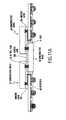
- FIG. 1 ( a )is a cross section of a conventional flip chip BGA using the flip chip technique.
- the flip chip techniqueemploys semiconductor device 1 having bumps (projecting electrodes) 13 formed on electrodes 12 of semiconductor chip 11 .
- Bumps 13are made of Au, Cu, Pb—Sn or the like, and formed with photolithography and plating.
- Semiconductor device 1is bonded face down to interposer 14 .
- bumps 13are electrically connected through metal junction to bonding pads 16 formed at respective portions of copper wiring 15 on the surface of interposer 14 .
- the flip chip techniquean increased number of pins, a reduced area for mounting, a higher speed of signal processing can be realized in semiconductor chips.
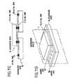
- FIG. 1 ( b )is a cross section of a conventional flip chip BGA using the flip chip technique and the underfill technique.
- the underfill techniqueis realized such that after semiconductor device 1 is mounted on interposer 14 , underfill resin 17 such as an epoxy resin is filled between semiconductor chip 11 and interposer 14 to protect the surface of semiconductor chip 11 and to reinforce the surroundings of bumps 13 , thereby achieving higher reliability of connection.
- the underfill techniqueinvolves a problem in that a smaller pitch of electrodes 12 (fine pitch), an accompanying smaller size of bumps 13 , and a smaller gap between semiconductor chip 11 and interposer 14 result in difficulties in completely filling underfill resin 17 between semiconductor chip 11 and interposer 14 and in checking whether or not any unfilled portion (void) is present after mounting.
- a method capable of solving such a problemis disclosed, for example, in Japanese Patent Laid-open Publication No. 5-3183.
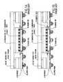
- bumps 13are first provided on electrodes 12 of many semiconductor chips 11 which are allocated to semiconductor wafer 20 (FIG. 2 ( b )).
- a resinis applied to the surface of semiconductor wafer 20 (semiconductor chip 11 ) to form protection film 18 .
- protection film 18is cured (FIG. 2 ( c )).
- the back of semiconductor wafer 20 (semiconductor chip 11 )is polished to thin the chip (FIG. 2 ( d )). Protection film 18 is polished to expose the surfaces of bumps 13 , thereby completing semiconductor device 2 .
- bumpsare provided also on the interposer for bonding to bumps 13 .
- the surface of semiconductor chip 11is covered and protected securely. Only good items can be mounted on an interposer by performing electrical selection, and the method is suitable for providing a smaller thickness since the polishing of semiconductor wafer 20 (semiconductor chip 11 ) after the formation of protection resin 18 can produce a thin chip of up to approximately 50 ⁇ m. In addition, even when any defect occurs after the mounting on an interposer, replacement is readily made individually since the device is not completely fixed to the interposer by an epoxy resin or the like.
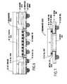
- Japanese Patent Laid-open Publication No. 11-26642discloses a method in which semiconductor device 70 having bumps 80 , adhesive sheet 98 having through-holes 102 , and interposer 72 B having connection holes 96 are manufactured individually before they are assembled. According to the method, after bumps 80 are aligned with connection holes 96 , adhesive sheet 98 is interposed between semiconductor device body 70 and interposer 72 B such that through-holes 102 are interposed between opposing bumps 80 and connection holes 96 . Semiconductor device 70 is pressed against interposer 72 B, bumps 80 are passed through through-holes 102 and connected to connection holes 96 , and they are bonded and fixed to each other (see FIG. 3 ).
- Japanese Patent Laid-open Publication No. 11-26642discloses a method in which an anisotropic conductive film is used instead of adhesive sheet 98 .
- Japanese Patent Laid-open Publication No. 8-102474discloses a method in which after an adhesive is applied to a main surface of a semiconductor chip on which electrodes are formed, part of the adhesive on the electrodes is removed to form holes in the adhesive layer through which the electrodes are exposed, and then bumps are filled into the holes.
- the adhesive layeris formed of a photosensitive resin such as polyimide or epoxy on the entire one surface of the semiconductor wafer, and the holes are formed through chemical etching in the portions of the adhesive layer where the electrode pads are to be exposed. Then, metal such as Au is filled into the holes through plating or the like.
- bumps 13 and semiconductor chip 11 fixed by protection film 18provide reliability in the junction surface of semiconductor chip 11 and bumps 13 at the time of mounting on a substrate.
- sufficient reliabilitycannot be ensured for bonding to such interposers.
- thinner semiconductor chip 11may cause thermal stress and warp stress applied to semiconductor chip 11 from the junction to destroy semiconductor chip 11 itself. This is because thermal stress and mechanical stress at the time of mounting on various interposers applied only to connection terminals (bumps) result in high dependence on the arrangement of the terminals, the number of pins, the size of a chip (package), the thickness of the chip and the like.
- adhesive sheet 98is adhered to both semiconductor device 70 and interpose 72 B and reinforces the surroundings of bumps 80 , thereby making it possible to ensure reliability of bonding.
- a conventional BGA type semiconductor package of a flip chip methodemploys a build-up BT substrate as an interposer to support a significantly small pad pitch of 200 ⁇ m of a semiconductor chip.
- the build-up BT substrateis expensive to raise concern about a high proportion of its cost to the product price. Thus, inexpensive alternative means or method is desired.
- the present inventionhas been made in view of the aforementioned prior art problems, and it is an object thereof to enable reliably mounting of a high-density type semiconductor device having a small pitch equal to a bare chip on an interposer or a mounting substrate (hereinafter referred to as “interposer”)) with flip chip bonding for forming and connecting metal bumps between electrodes (bonding pads) of a semiconductor chip and leads, and to provide a semiconductor device at low cost by providing a simpler mounting structure, easier mounting, a reduced number of mounting steps, and improved yields.
- interposera mounting substrate
- a semiconductor devicecomprising a semiconductor chip, a stud bump provided on an electrode of the semiconductor chip, and an adhesive layer provided on the surface of the semiconductor chip on which the electrode is formed, wherein the stud bump projects from a surface of the adhesive layer.
- the semiconductor device of the first aspect of the present inventionsince the stud bump is selected, the wire bonding technique can be applied.
- the semiconductor devicehas the advantage of the capability of dealing with individual cases to readily allow flexible manufacture.
- the stud bumpcan be thermocompression-bonded to a lead on an interposer or the like as it is (without providing a bump on the lead) since the bump projects from the surface of the adhesive layer.
- the adhesive layerreinforces the stud bump from the surroundings and no load is applied on the stud bump at the time of mounting.
- the adhesive layerprovides complete sealing between the semiconductor chip and the interposer.
- the semiconductor chip of the first aspecthas advantages of ensuring sufficient reliability without using an underfill, allowing easy mounting of a high-density type semiconductor device having a small pitch equal to a bare chip on an interposer or the like with a simple structure and simple steps, providing improved yields, and enabling manufacture at low cost.
- a semiconductor deviceobtained by bonding the semiconductor device according to the first aspect of the present invention to an interposer through thermocompression bonding.
- the semiconductor device according to the second aspect of the present inventionhas advantages of high reliability and low cost as described above due to the use of the semiconductor device of the first aspect of the present invention.
- an MCM of high-density packagingcan be obtained.
- a semiconductor devicecomprising a semiconductor chip, a protection resin layer provided on the surface of the semiconductor chip on which an electrode is formed, a bump provided on the electrode of the semiconductor chip and exposed at a surface of the protection resin layer, and an interposer adhered to the surface of the protection resin layer through a cured flux and electrically connected to the bump.
- the semiconductor devicehas the advantage of fixing the semiconductor chip securely to the interposer to ensure high reliability of bonding since the cured flux is provided between the protection resin layer and the interposer such that the flux is bonded to both of them.
- a thermosetting flux used for connection of the bump to the interposeradds no steps or need of an underfill.
- a semiconductor deviceobtained by providing a device hole in the interposer in the semiconductor device of the second or third aspect of the present invention.
- the device holerefers to a hole provided in the surface of the interposer on which the semiconductor chip is mounted, except the area on which pad electrodes are mounted.
- the semiconductor devicehas the advantage of being capable of preventing damage to the interface between the interposer and the adhesive layer due to the popcorn phenomenon since the interposer is provided with the device hole, and the advantage of eliminating the need of filling or providing a protection resin such as an underfill after the mounting of the semiconductor chip on the interposer since the surface of the semiconductor chip exposed through the device hole is resin-sealed by the adhesive layer.
- a semiconductor devicecomprising a semiconductor chip, an adhesive layer provided on the surface of the semiconductor chip on which an electrode is formed, a bump provided on the electrode of the semiconductor chip and exposed at a surface of the adhesive layer, a wiring pattern adhered to the surface of the adhesive layer and partially bonded to the bump, and an insulating and covering layer for insulating and covering the wiring pattern and selectively opening to form an external connecting portion.
- the semiconductor devicesince only the wiring pattern and the insulating and covering layer correspond to an interposer, an expensive material such as polyimide, BT resin, or ceramic used as a base material of the interposer is not used and it is possible to provide the function of the interposer, i.e. the function of being interposed between the semiconductor chip and the mounting substrate to provide terminals arranged with a greater pitch than that of the pad electrodes for allowing mounting on the mounting substrate.
- the semiconductor devicehas the advantage of eliminating the need of using an existing interposer to enable manufacture at low cost.
- the semiconductor devicehas the advantage of fixing the wiring pattern with the adhesive layer to ensure high reliability of bonding.
- a semiconductor devicecomprising a semiconductor chip, a protection resin layer provided on the surface of the semiconductor chip on which an electrode is formed, a bump provided on the electrode of the semiconductor chip and exposed at a surface of the protection resin layer, a wiring pattern adhered to the surface of the protection resin layer through a cured flux and partially bonded to the bump, and an insulating and covering layer for insulating and covering the wiring pattern and selectively opening to form an external connecting portion.
- the semiconductor devicesince only the wiring pattern and the insulating and covering layer correspond to an interposer, an expensive material such as polyimide, BT resin, or ceramic used as a base material of the interposer is not used and it is possible to provide the function of the interposer, i.e. the function of being interposed between the semiconductor chip and the mounting substrate to provide terminals arranged with a greater pitch than that of the pad electrodes for allowing mounting on the mounting substrate.
- the semiconductor devicehas the advantage of eliminating the need of using an existing interposer to enable manufacture at low cost.
- the semiconductor devicehas the advantage of fixing the wiring pattern with the cured flux to ensure high reliability of bonding.
- a thermosetting flux used for connection of the bump to the wiring patternadds no steps or need of an underfill.
- a semiconductor apparatuscomprising, two or more semiconductor devices, each of the devices including a semiconductor chip, an adhesive layer provided on the surface of the semiconductor chip on which an electrode is formed, and a bump provided on the electrode of the semiconductor chip and exposed at a surface of the adhesive layer, wherein part of the surface of one of the semiconductor devices on which the adhesive layer is provided is bonded to part or all of the surface of another one of the semiconductor devices on which the adhesive layer is provided and they are electrically connected to each other with the bumps at the bonding surface.
- the semiconductor apparatusis a multi chip module obtained by bonding the semiconductor chips such that the surfaces thereof on which the electrodes are formed are bonded to each other, and has advantages of high packaging density and ensuring high reliability of bonding with the adhesive layer. It is possible that an interposer or the like is adhered to the surface of the semiconductor device on which the adhesive layer is formed except the bonding surface of the semiconductor chips to bond the bump to a lead of the interposer in that area for mounting.
- a semiconductor apparatuscomprising, two or more stacked semiconductor devices, each of the devices including a semiconductor chip having electrodes formed on the front and back, an adhesive layer provided on the front or back of the semiconductor chip, and a bump provided on the electrode of the semiconductor chip and exposed at a surface of the adhesive layer, wherein upper one of the semiconductor devices is bonded to lower one of the semiconductor devices with the adhesive layer and the electrodes thereof are connected to each other through the bump.
- the semiconductor apparatusis a multi chip module obtained by bonding and stacking a plurality of the semiconductor chips and establishing electrical conduction through the bumps, and has advantages of high packaging density and ensuring high reliability of bonding with the adhesive layer.
- thermoplastic resin with adhesionas the adhesive layer in the semiconductor device according to the first, second, fifth, seventh, or eighth aspect of the present invention.
- the semiconductor devicehas the advantage of allowing individual replacement of a defective semiconductor chip after bonding since the adhesive layer is formed of the thermoplastic resin with adhesion and the semiconductor chip can be separated from the base material by heat applied to the adhesive layer. Particularly, since a defective item can be replaced even after a number of semiconductor chips are mounted on a single wiring substrate, the wiring substrate is not wasted.
- a method of manufacturing a semiconductor devicecomprising the steps of:
- the method of manufacturing a semiconductor chip according to the tenth aspect of the present inventionallows manufacture of a semiconductor device with a simple process which can readily realize reliable mounting to provide adhesion and electrical connection to the interposer or the like and to seal the junction.
- the adhesive layeris formed after the provision of the bump, it is not necessary to bore a hole in the adhesive layer and perform some processing. It is thus not necessary to form the adhesive layer through a number of processes such as mask design with a lithography technique, resist application, exposure, development, and etching. Required processing is providing the adhesive layer and etching after the provision of the bump by using the wire bonding technique.
- a method of manufacturing a semiconductor devicecomprising the steps of:
- the method of manufacturing a semiconductor deviceprovides advantages similar to those from the tenth aspect of the present invention and advantages of a significant reduction in the number of steps for manufacturing a semiconductor package and a significant reduction in the time required for the steps since the adhesion and electrical connection to an interposer are simultaneously performed to simultaneously achieve inner lead bonding of all electrodes on the semiconductor chip, and adhesion of the semiconductor chip to the wiring substrate and sealing of the junction surface.
- a conventional signal point bonding methodtakes a total of 3000 seconds assuming that bonding takes 0.1 second per electrode.
- bondingis completed in approximately 10 to 20 seconds, and adhesion is also completed at the same time, thereby achieving great advantages in terms of time and economics.
- the adhesive layercan provide high reliability of bonding to eliminate the need of using an underfill.
- the wiring substratecorresponds to a wiring tape, a plastic substrate, a ceramic substrate, a lead frame or the like.
- a method of manufacturing a semiconductor devicecomprising the steps of:
- thermosetting fluxfor one, or two or more of the semiconductor chips, applying a thermosetting flux to the bump and the protection resin layer or to a wiring substrate corresponding thereto;
- thermosetting flux
- the method of manufacturing a semiconductor deviceprovides advantages of a significant reduction in the number of steps for manufacturing a semiconductor package and a significant reduction in the time required for the steps similarly to the eleventh aspect of the present invention since the bump is bonded to the wiring on the wiring substrate with reflow and the cured flux interposed between the protection resin layer and the wiring substrate bonds the semiconductor chip to the wiring substrate to simultaneously achieve the adhesion and electrical connection to an interposer.
- the cured fluxcan provide high reliability of bonding to eliminate the need of using an underfill.
- a method of manufacturing a semiconductor devicecomprising the steps of:
- the method of manufacturing a semiconductor device according to the thirteenth aspect of the present inventionhas the advantage of reducing two dicing steps for the semiconductor wafer and for the wiring substrate to one since the semiconductor chip is cut with the wiring substrate bonded thereto.
- the method of manufacturing a semiconductor deviceallows simple manufacture of a CSP in which a semiconductor chip and an interposer have the same area and are completely stacked.
- a semiconductor chipmay be mounted on a wiring substrate after division into each of semiconductor chips as in the eleventh aspect of the present invention.
- the adhesive layercan provide high reliability of bonding to eliminate the need of using an underfill.
- a fourteenth aspect of the present inventionthere is provided a method of manufacturing a semiconductor device, comprising the steps of:
- the method of manufacturing a semiconductor chip according to the fourteenth aspect of the present inventionprovides advantages similar to those of the thirteenth aspect of the present invention and advantages of a significant reduction in the number of steps for manufacturing a semiconductor package and a significant reduction in the time required for the steps since the adhesion and electrical connection to an interposer are simultaneously performed to simultaneously achieve inner lead bonding of all electrodes on the semiconductor chip, and adhesion of the semiconductor chip to the wiring substrate and sealing of the junction surface.
- the adhesive layercan provide high reliability of bonding to eliminate the need of using an underfill.
- a method of manufacturing a semiconductor devicecomprising the steps of:
- thermosetting fluxto the bump and the protection resin layer or to a wiring substrate corresponding thereto;
- the method of manufacturing a semiconductor device according to the fifteenth aspect of the present inventionprovides advantages similar to those of the thirteenth aspect of the present invention and advantages of a significant reduction in the number of steps for manufacturing a semiconductor package and a significant reduction in the time required for the steps similarly to the eleventh aspect of the present invention since the bump is bonded to the wiring on the wiring substrate with reflow and the cured flux interposed between the protection resin layer and the wiring substrate bonds the semiconductor chip to the wiring substrate to simultaneously achieve the adhesion and electrical connection to an interposer.
- the cured fluxcan provide high reliability of bonding to eliminate the need of using an underfill.
- a sixteenth aspect of the present inventionthere is provided a method of manufacturing a semiconductor device, comprising the steps of:
- the method of manufacturing a semiconductor deviceprovides the advantage of reduced cost since the wiring pattern for connecting the semiconductor chip to a mounting substrate is formed by using the semiconductor chip as a base to eliminate the need of using an additional interposer and thus the need of the material and process thereof, and the advantage of providing a thinner semiconductor package.
- the adhesive layercan provide high reliability of bonding to eliminate the need of using an underfill.
- a method of manufacturing a semiconductor devicecomprising the steps of:
- the method of manufacturing a semiconductor deviceprovides the advantages of the sixteenth aspect of the present invention and advantages of a significant reduction in the number of steps for manufacturing a semiconductor package and a significant reduction in the time required for the steps since the adhesion and electrical connection to the metal foil are simultaneously performed to simultaneously achieve inner lead bonding of all electrodes on the semiconductor chip, and adhesion of the semiconductor chip to the metal foil and sealing of the junction surface.
- a method of manufacturing a semiconductor devicecomprising the steps of:
- thermosetting flux
- the method of manufacturing a semiconductor device according to the eighteenth aspect of the present inventionprovides advantages similar to those of the sixteenth aspect of the present invention and advantages of a significant reduction in the number of steps for manufacturing a semiconductor package and a significant reduction in the time required for the steps since the bump is bonded to the wiring on the wiring substrate with reflow and the cured flux interposed between the protection resin layer and the wiring substrate bonds the semiconductor chip to the wiring substrate to simultaneously achieve the adhesion and electrical connection to an interposer.
- the cured fluxcan provide high reliability of bonding to eliminate the need of using an underfill.
- a method of manufacturing a semiconductor devicecomprising the steps of:
- the method of manufacturing a semiconductor deviceprovides the advantage of reduced cost since the semiconductor chip is provided with the wiring pattern for connecting the semiconductor chip to a mounting substrate in the process on the semiconductor wafer to eliminate the need of using an additional interposer and thus the need of the material and process thereof, and the advantage of providing a thinner semiconductor package.
- the adhesive layercan provide high reliability of bonding to eliminate the need of using an underfill.
- a method of manufacturing a semiconductor devicecomprising the steps of:
- the method of manufacturing a semiconductor deviceprovides the advantages of the nineteenth aspect of the present invention and advantages of a significant reduction in the number of steps for manufacturing a semiconductor package and a significant reduction in the time required for the steps since the adhesion and electrical connection to the metal foil are simultaneously performed to simultaneously achieve inner lead bonding of all electrodes on the semiconductor chip, and adhesion of the semiconductor chip to the metal foil and sealing of the junction surface.
- a method of manufacturing a semiconductor devicecomprising the steps of:
- thermosetting flux
- the method of manufacturing a semiconductor deviceprovides the advantages of the nineteenth aspect of the present invention and advantages of a significant reduction in the number of steps for manufacturing a semiconductor package and a significant reduction in the time required for the steps since the bump is bonded to the wiring on the wiring substrate with reflow and the cured flux interposed between the protection resin layer and the wiring substrate bonds the semiconductor chip to the wiring substrate to simultaneously achieve the adhesion and electrical connection to an interposer.
- the cured fluxcan provide high reliability of bonding to eliminate the need of using an underfill.
- a method of manufacturing a semiconductor device of any one of the sixteenth to twenty-first aspects of the present inventionin which an insulating and covering layer is selectively formed on the wiring pattern after the metal foil is formed on the wiring pattern.
- the insulating and covering layer selectively formed on the wiring patterninsulates and covers the wiring pattern, and an opening in the insulating and covering layer exposes part of the wiring pattern to form an electrode (land portion) for electrical connection to the outside.
- the devicemay be used as an LGA type package.
- a method of manufacturing a semiconductor device of the twenty-second aspect of the preset inventionin which after the insulating and covering layer is selectively formed on the wiring pattern, a solder ball is provided on a land portion of the wiring pattern exposed through an opening of the insulating and covering layer.
- the method of manufacturing a semiconductor deviceprovides a BGA type package.
- a method of manufacturing a semiconductor device of the tenth, eleventh, thirteenth, fourteenth, sixteenth, seventeenth, nineteenth or twentieth aspect of the present inventionin which the adhesive layer is a thermoplastic resin with adhesion.
- the method of manufacturing a semiconductor deviceprovides the advantage of being capable of replacing a defective semiconductor chip individually after the adhesion since the adhesive layer is a thermoplastic resin with adhesion and thus the semiconductor chip can be separated from the base material by adding heat to the adhesive layer.
- the methodprovides the advantage of preventing wasted wiring substrates.
- a semiconductor devicecomprising a semiconductor chip, an adhesive layer provided on the surface of the semiconductor chip on which an electrode is formed, a bump provided on the electrode of the semiconductor chip and exposed at a surface of the adhesive layer, a tape substrate, and an interposer, wherein the semiconductor chip is adhered to the front of the tape substrate with the adhesive layer, the semiconductor chip is electrically connected to the tape substrate with the bump, and the interposer is connected to the back of the tape substrate for allowing electrical conduction.
- the present inventionproduces the effect of allowing low-cost manufacture of a high density package (hereinafter abbreviated as “HDP”)) which realizes reliable bonding by forming the bump for electrical connection and the adhesive resin having the adhesion function on the semiconductor chip.
- HDPhigh density package
- the HDPWhen the HDP is mounted on another BGA substrate or the like to manufacture a package larger than the semiconductor chip, an underfill step for injecting a resin between the semiconductor chip and the substrate is not required since the adhesive layer adheres to the BGA substrate or the like to provide sealing between the semiconductor chip and the substrate. For this reason, the HDP with a smaller pitch can be mounted reliably on an interposer or the like to achieve a simpler mounting structure, easier mounting, a reduced number of steps for mounting, and improved yields.
- the present inventionthus provides the effect of manufacturing a semiconductor package such as a CSP with reliability of mounting.
- the present inventionadvantageously facilitates replacement after mounting to prevent expensive wiring substrates from being wasted.
- the interposeris formed directly on the semiconductor wafer to reduce the number of steps for manufacturing the interposer and the material cost of the interposer.
- the present inventionproduces the effect of being capable of providing various semiconductor packages at low cost.
- the present inventionadvantageously provides a high-density packaging multi chip module with high reliability and at low cost by using a plurality of HDPs such that they are partially bonded to each other or they are laminated and bonded to each other.
- the bump and the adhesive resinare formed on the semiconductor chip as a wafer, efficient manufacture can be performed.
- thermocompression bonding or reflow processingin combination with a thermosetting flux when the semiconductor device is mounted on the BGA substrate or the like, thereby leading to favorable efficiency of manufacture.
- the present inventioncan readily support flexible manufacturing since the wire bonding technique is applicable to the bump formation.
- FIGS. 1 ( a ), ( b )are cross sections showing semiconductor devices of conventional examples
- FIGS. 2 ( a ) to ( d )are cross sections illustrating steps for describing a semiconductor device of a conventional example and a manufacturing method thereof;
- FIG. 3is a cross section for describing a semiconductor device of a conventional example and a manufacturing method thereof;
- FIGS. 4 ( a ) to ( d )are cross sections illustrating steps for describing a semiconductor device according to Embodiment 1 of the present invention and a manufacturing method thereof;
- FIG. 5 ( a )is a cross section showing a semiconductor device according to Embodiment 2 of the present invention
- FIG. 5 ( b )is a cross section showing a semiconductor device according to Embodiment 3 of the present invention
- FIG. 6is a cross section showing a semiconductor device according to Embodiment 4 of the present invention.
- FIG. 7is a cross section showing a semiconductor device according to Embodiment 5 of the present invention.
- FIGS. 8 ( a ) to ( d )are cross sections illustrating steps for describing a semiconductor device according to Embodiment 6 of the present invention and a manufacturing method thereof;
- FIGS. 9 ( a ) and ( b )are cross sections illustrating applications of the semiconductor device according to Embodiment 6 of the present invention.
- FIGS. 10 ( a ) and ( b )are cross sections showing other applications of the semiconductor device according to Embodiment 6 of the present invention.
- FIG. 11 ( a )is a cross section showing a semiconductor device according to Embodiment 7 of the present invention
- FIG. 11 ( b )is a perspective view showing a semiconductor device according to Embodiment 8 of the present invention
- FIG. 11 ( c )is a cross section taken along the A face in FIG. 11 ( b );
- FIG. 12is a cross section showing a semiconductor device according to Embodiment 9 of the present invention.
- FIG. 13is a cross section showing a semiconductor device according to Embodiment 10 of the present invention.
- FIGS. 4 ( a ) to ( d )are cross sections illustrating steps for describing the semiconductor device and the manufacturing method of Embodiment 1 of the present invention.
- semiconductor device 3 (HDP: High Density Package) of Embodiment 1comprises semiconductor chip 11 , Au ball bumps 21 provided on pad electrodes 12 with a stud bump method, and thermoplastic adhesive layer 22 disposed on the surface of semiconductor chip 11 on which pad electrodes 12 are formed such that the tops of Au ball bumps 21 project from the surface of adhesive layer 22 .
- adhesive layer 22is formed of a thermoplastic adhesive in consideration of replacement of a defective item after adhesion
- a thermosetting adhesivemay be used instead of the thermoplastic adhesive if such replacement is not required.
- FIGS. 4 ( a ) to ( d )are enlarged views showing one particular semiconductor chip 11 formed in semiconductor wafer 20 .
- Au ball bumps 21are provided on pad electrodes 12 of each semiconductor chip 11 .
- Au ball bumps 21are stud bumps formed with the stud bump method which is an application of the wire bonding technique. Specifically, a wire bonding apparatus is used to form a gold ball at the end of a gold wire extending from a capillary and the gold ball is pressed against pad electrode 12 . The capillary is ultrasonically vibrated to ultrasonically weld the gold ball to pad electrode 12 and then the gold wire is cut. As above, Au ball bumps 21 are formed on pad electrodes 12 (FIG. 4 ( b )).
- thermoplastic PI resinfor example, is applied at a thickness of approximately 50 ⁇ m to the surface on which Au ball bumps 21 are disposed, and the resin is cured temporarily to the extent that fluidity is lost to provide adhesive layer 22 (FIG. 4 ( c )).
- semiconductor device 3 before isolationis obtained through the aforementioned steps. Thereafter, semiconductor wafer 20 is cut for division into semiconductor devices 3 for use in the next step, or used in the next step as it is, as later described.
- FIG. 5 ( a )is a cross section showing the semiconductor device of Embodiment 2 of the present invention.
- the semiconductor device shown in FIG. 5 ( a )is a semiconductor device (BGA type semiconductor package) in which semiconductor device 3 is bonded to wiring tape 23 as an interposer through thermocompression bonding and resin molding is performed.
- semiconductor wafer 20(see FIG. 4) is first cut for division into individual semiconductor devices 3 .
- one, or two or more semiconductor devices 3are mounted on one wiring tape 23 , and heating and pressing are performed to establish adhesion to wiring tape 23 with adhesive layer 22 and electrical connection to copper wiring 24 on wiring tape 23 with Au ball bumps 21 .
- adhesion and connectionmay be performed as follows.
- Wiring tape 23 used in this caseis configured such that copper wiring 24 is supported by insulating film 25 at the positions corresponding to pad electrodes 12 , i.e. such that holes for applying a bonding tool are not provided in insulating film 25 at the positions corresponding to pad electrodes 12 . This is because Embodiment 2 does not employ a single point bonding method with a bonding tool.
- Wiring tape 23is first disposed on a silicon sheet (not shown) with a thickness of approximately 0.2 to 1.0 mm, and semiconductor device 3 is positioned and mounted on Au plated pads 26 on copper wiring 24 . Then, a vacuum is produced for the surrounding atmosphere.
- a heater plate(not shown) is pulled down from above and pressed against the backs (the opposite sides of the surfaces on which the electrodes are formed) of a number of semiconductor chips 11 .
- wiring tape 23is pressed against almost the entire surface of each semiconductor chip 11 on which pad electrodes 12 are formed while heat is added to adhesive layer 22 and an inner lead connecting portion including Au ball bumps 21 .
- Au ball bumps 21are melted and adhesive layer 22 is cured as described above, thereby completing the metal junction between Au plated pads 26 and Au ball bumps 21 and the adhesion of semiconductor chip 11 to wiring tape 23 with adhesive layer 22 .
- the vacuum atmosphereproduces no voids between the surface of semiconductor chip 11 on which pad electrodes 12 are formed and adhesive layer 22 . As the size of a chip becomes larger, concern about voids increases. In such a case, adhesion in the vacuum atmosphere is effective as in the embodiment.
- Au plated pads 26may be bonded to Au ball bums 21 to readily establish electrical conduction under conditions, for example, at 270° C., for 10 seconds, and at 980 mN/bump.
- the wiring tape on which semiconductor device 3 is mountedis transferred to a resin molding apparatus and put in a mold, and the surface of wiring tape 23 to which semiconductor device is bonded is sealed by a resin.
- sealing resin 27is cured, cover resist 50 is formed, solder balls 31 are formed, and dicing into individual packages is performed.
- the semiconductor device (BGA type semiconductor package) shown in FIG. 5 ( a )is obtained.
- FIG. 5 ( a )shows a single chip package
- a plurality of semiconductor devices 3may be arranged in a single package to provide a multi chip package.
- Another effective manufacturing processis that, before semiconductor wafer 20 is cut for division into individual semiconductor devices 3 , semiconductor wafer 20 is adhered to wiring tape 23 through adhesive layer 22 and then semiconductor chip 11 is cut along its perimeter for division into individual pieces.
- a resulting semiconductor packageis configured such that each end face of semiconductor chip 11 is flush with each end face of wiring tape 23 as the same cut surface.
- FIG. 5 ( b )is a cross section showing the semiconductor device of Embodiment 3 of the present invention.
- the semiconductor device shown in FIG. 5 ( b )comprises semiconductor chip 11 , adhesive layer 22 as a protection resin layer provided on the surface on which pad electrodes 12 are formed, Au ball bums 21 formed on pad electrodes 12 and exposed at the surface of adhesive layer 22 , and wiring tape 23 adhered to the surface of adhesive layer 22 through cured flux 28 and serving as an interposer for electrical connection to Au ball bumps 21 .
- the semiconductor deviceis a semiconductor device (BGA type semiconductor package) manufactured by bonding semiconductor device 3 to wiring tape 23 with thermocompression bonding and performing resin molding.
- thermosetting flux 28is applied to Au ball bums 21 and adhesive layer 22 , or thermosetting flux 28 is applied to wiring tape 23 corresponding thereto.
- Au ball bumps 21are disposed on solder plated pads 29 formed by solder plating of part of copper wiring 24 of wiring tape 23 .
- wiring tape 23 on which semiconductor device 3 is mountedis transferred to a resin molding apparatus and put in a mold, and the surface of wiring tape 23 to which semiconductor device 3 is bonded is sealed by a resin.
- sealing resin 27is cured, cover resist 50 is formed, solder balls 31 are provided, and dicing into individual packages is performed.
- the semiconductor device (BGA type semiconductor package) shown in FIG. 5 ( b )is obtained.
- FIG. 5 ( b )shows a single chip package
- a plurality of semiconductor devices 3may be arranged in a single package to provide a multi chip package.
- thermosetting flux 28is applied to Au ball bumps 21 on semiconductor wafer 20 and adhesive layer 22 , or thermosetting flux 28 is applied to wiring tape 23 corresponding thereto.
- Au ball bumps 21are disposed on solder plated pads 29 and heated to solder Au ball bums 21 to solder plated pads 29 and cure thermosetting flux 28 .
- semiconductor chip 11is cut along its perimeter for division into individual pieces. In this case, a resulting semiconductor package is configured such that each end face of semiconductor chip 11 is flush with each end face of wiring tape 23 as the same cut surface.
- FIG. 6is a cross section showing the semiconductor device of Embodiment 4 of the present invention.
- the semiconductor device of Embodiment 4is a multi chip module in which a plurality of semiconductor devices 3 are mounted on interposer 14 in the same manner as Embodiment 2, and heat spreader 32 is bonded to the back of semiconductor devices 3 through heat radiation pastes 30 .
- Such a configurationcan result in a multi chip module with a high level of heat radiation.
- thermosetting fluxas in Embodiment 3.
- solder plated padsreceive Au ball bumps 21 and the thermosetting flux bonds adhesive layer 22 serving as a protection resin layer to copper wiring 15 .
- FIG. 7is a cross section showing the semiconductor device of Embodiment 5 of the present invention.
- the semiconductor device of Embodiment 5is configured such that semiconductor device 3 is mounted on wiring tape 33 provided with device hole 34 as an interposer in the same manner as Embodiment 2.
- mountingmay be performed with reflow using a thermosetting flux as in Embodiment 3.
- solder plated padsreceive Au ball bumps 21 and the thermosetting flux bonds adhesive layer 22 serving as a protection resin layer to copper wiring 35 .
- adhesive layer 22adheres to wiring tape 33 on the periphery of semiconductor device 3 , and Au ball bumps 21 bonds to Au plated pads 36 on copper wiring 35 to establish electrical connection.
- the central portion of semiconductor device 3is exposed through device hole 34 .
- device hole 34 provided in wiring tape 33prevents the damage to the interface between wiring tape 33 and adhesive layer 22 due to a popcorn phenomenon. Since the surface of semiconductor chip 11 in the area corresponding to device hole 34 is resin sealed by adhesive layer 22 , it is not necessary to fill or provide a protection resin such as an underfill after the semiconductor chip is mounted on the wiring tape.
- FIGS. 8 ( a ) to ( d )are cross sections illustrating steps for describing the semiconductor device and the manufacturing method of Embodiment 6 of the present invention.
- the semiconductor device of Embodiment 6comprises semiconductor device 3 including semiconductor chip 11 , adhesive layer 22 disposed on the surface on which pad electrodes 12 are formed, and Au ball bumps 21 provided on pad electrodes 12 and exposed at the surface of adhesive layer 22 , copper wiring 42 adhered to the surface of adhesive layer 22 and bonded partially to Au ball bumps 21 , and cover resist 43 serving as an insulating and covering layer for insulating and covering copper wiring 42 and selectively opening to form an external connecting portion.
- the semiconductor deviceis a BGA type semiconductor package having solder balls 31 formed as external terminals.
- Au ball bumps 21establish Au—Au metal junction with Au plated pads 44 on copper wiring 42 .
- the semiconductor device of Embodiment 6is manufactured as follows. As shown in FIG. 8 ( a ), copper foil 41 , for example with a thickness of 50 ⁇ m, is first prepared.
- Copper foil 41is aligned with semiconductor device 3 through adhesive layer 22 , and heating and pressing are performed by a heater plate in a vacuum atmosphere in the same manner as Embodiment 2.
- adhesive layer 22adheres semiconductor device 3 to copper foil 41 , and Au ball bumps 21 are bonded to copper foil 41 through Au plated pads 44 to establish electrical connection.
- copper foil 41is formed into a predetermined pattern through a lithography technique to obtain copper wiring 42 .
- cover resist 43is applied as an insulating and covering layer to copper wiring 42 , and exposure and development are performed to form openings therein, thereby exposing land portions of copper wiring 42 for disposing solder balls 31 .
- solder balls 31are mounted and provided on the land portions through reflow.
- semiconductor wafer 20(see FIG. 4) having semiconductor devices 3 formed therein before isolation is aligned with copper foil 41 through adhesive layer 22 , heating and pressing are performed to achieve adhesion to copper foil 41 with adhesive layer 22 and electrical connection to copper foil 41 with Au ball bumps 21 , copper foil 41 is formed into a wiring pattern, and then semiconductor wafer 20 is cut along the perimeter of semiconductor chips 11 for division into individual pieces.
- a resulting BGA type semiconductor packagehas the same size as the outer size of the package or the outer size of semiconductor chip 11 .
- semiconductor wafer 20 having semiconductor device 3 or many semiconductor devices 3 formed thereinmay be bonded to copper foil 41 with reflow using a thermosetting flux.
- solder plated padsreceive Au ball bumps 21 and the thermosetting flux bonds adhesive layer 22 serving as a protection resin layer to copper foil 41 .
- resin moldingmay be performed such that sealing resin 27 seals semiconductor device 3 . This protects semiconductor chip 11 .
- heat spreader 40having a ceiling portion and a wall portion is connected to semiconductor chip 11 through heat radiation paste 45 such that the inner surface of the ceiling portion is bonded to the back of semiconductor chip 11 , and the lower ends of the wall portion are bonded to cover resist 43 filled between copper wirings 42 by heat spreader fixing adhesive 46 .
- Thisprovides a higher level of heat radiation.
- the multi chip modulemay be resin molded to seal semiconductor devices 3 a , 3 b by sealing resin 47 . This protects semiconductor chips 11 .
- FIG. 11 ( a )is a cross section showing the semiconductor device of Embodiment 7 of the present invention.
- the semiconductor device of Embodiment 7is a multi chip module comprising three semiconductor devices 3 c , 3 d , and 3 e in which part of the surface of semiconductor device 3 c on which adhesive layer 22 c is provided is adhered to part of the surface of semiconductor device 3 d on which adhesive layer 22 d is provided, they are electrically connected to each other at the bonding surface by Au ball bumps 21 , part of the surface of semiconductor device 3 e on which adhesive layer 22 e is provided is adhered to part of the surface of semiconductor device 3 d on which adhesive layer 22 d is provided, and they are electrically connected to each other at the bonding surface with Au ball bumps 21 .
- Interposer 48is bonded to the area of the surface of semiconductor device 3 c on which adhesive layer 22 c is provided except the bonding surface to semiconductor device 3 d and to the area of the surface of semiconductor device 3 e on which adhesive layer 22 e is provided except the bonding surface to semiconductor device 3 d , and Au ball bumps 21 are bonded to leads of interposer 48 in those areas for mounting.
- Semiconductor device 3 dis inserted into hole 51 provided in interposer 48 .
- the shown structuremay be protected by resin sealing.
- FIG. 11 ( b )is a perspective view showing the semiconductor device of Embodiment 8 of the present invention
- FIG. 11 ( c )is a cross section taken along the A face in FIG. 11 ( b ).
- the semiconductor device of Embodiment 8is a multi chip module comprising two semiconductor devices 3 f , 3 g in which part of the surface of semiconductor device 3 g on which adhesive layer 22 g is provided is adhered to the entire surface of semiconductor device 3 f on which adhesive layer 22 f is provided and they are electrically connected to each other at the bonding surface with their Au ball bumps 21 as shown in FIG. 11 ( c ).
- An interposer(not shown) is bonded to the areas of the surface of semiconductor device 3 g on which adhesive layer 22 g is provided except the bonding surface to semiconductor device 3 f (the areas present on both sides of semiconductor device 3 f in FIGS. 11 ( b ), 11 ( c )), and Au ball bumps 21 a are bonded to leads of the interposer in those areas for mounting.
- Semiconductor device 3 fis inserted into a hole provided in the interposer in the same manner as Embodiment 7.
- resin sealingmay be performed for protection.
- FIG. 12is a cross section showing the semiconductor device of Embodiment 9 of the present invention.
- semiconductor device 4is bonded to wiring tape 23 .
- Semiconductor device 4is configured to include semiconductor chip 5 having pad electrodes formed on the front and back, unlike semiconductor device 3 used in Embodiment 2. Electrical conduction is established between front pad electrode 12 a and back pad electrode 12 b through aluminum wiring 49 .
- the semiconductor device of Embodiment 9is a multi chip module in which four semiconductor devices 4 are stacked by adhesion through adhesive layers 22 , and Au ball bumps 21 of one semiconductor device 4 are bonded to pad electrodes 12 b on the back surface of semiconductor device 4 below for electrical connection.
- the semiconductor devicehas a high packaging density and high reliability of bonding with adhesive layers 22 .
- resin sealingmay be performed for protection.
- a plating methodmay be used instead.
- plated bumpsare formed as follows. Specifically, a resist is applied to semiconductor wafer 20 , and exposure and development are performed to form a resist pattern having openings on pad electrodes 12 . Next, metal is deposited in the openings though the plating method to form bumps. Then, the resist is removed.
- the plating methodis suitable for mass production, while the stud bump method is suitable for flexible manufacturing. Whether the stud bump method or plating method is used depends on the quantity of manufacture.
- the material of the bumps formed on the chipis not limited to Au, and Cu, Pb—Sn or the like may be used as the material.
- FIG. 13is a cross section showing the semiconductor device of Embodiment 16 of the present invention.
- the semiconductor device of Embodiment 10comprises semiconductor device 3 , tape substrate 52 , and interposer 14 , in which semiconductor device 3 is mounted on interposer 14 through tape substrate 52 .
- Tape substrate 52is a wiring tape in tape carrier shape obtained by forming copper wiring 54 in a predetermined pattern through a lithography technique on the front and back of insulating film 53 made of polyimide. Insulating film 53 is provided with through-holes for allowing electrical conduction between copper wirings 54 on the front and back. Au plated pads 55 are provided on part of copper wiring 54 formed on the surface of tape substrate 52 . Copper wiring 54 formed on the back of tape substrate 52 is insulated by and covered with cover resist 56 except land portions.
- Semiconductor device 3is adhered to the surface of tape substrate 52 with adhesive layer 22 and electrical connection is made between them through Au ball bumps 21 .
- Each Au ball bump 21is disposed on pad electrode 12 of semiconductor chip 11 and has one end connected to pad electrode 12 and the other end connected to Au plated pad 55 .
- Adhesive layer 22provides sealing between semiconductor chip 11 and tape substrate 52 , and sealing even of Au ball bumps 21 for ensuring reliable mounting. Adhesive layer 22 also functions to protect the surface of semiconductor chip 11 .
- Solder balls 57are provided on the land portions of copper wiring 54 of the back of tape substrate 52 . Each solder ball 57 has one end connected to the land portion of copper wiring 54 and the other end connected to solder plated pad 59 formed by solder plating on interposer 14 for electrically connecting tape substrate 52 with interposer 14 . Cured thermosetting flux 58 is filled between tape substrate 52 and interposer 14 around solder balls 57 for reinforcing the junction between tape substrate 52 and interpose 14 to ensure reliable mounting.
- heat radiation paste 30is applied to the back of semiconductor chip 11 and heat spreader 32 is adhered to semiconductor chip 11 through heat radiation paste 30 .
- the semiconductor device of Embodiment 10is manufactured as follows.
- Semiconductor device 3is first manufactured as described in Embodiment 1.
- semiconductor device 3is thermocompression-bonded to the surface of tape substrate 52 as in Embodiment 2.
- thermosetting fluxas in Embodiment 3.
- solder balls 57are provided on the land portions on the back of tape substrate 52 .
- Thermosetting flux 58is then applied to the back of tape substrate 52 or the bonding area of interposer 14 .
- tape substrate 52 to which semiconductor device 3 is adheredis mounted on interposer 14 , heating is performed with infrared heating, hot air heating or the like, and reflow processing is performed. In this manner, solder balls 57 are soldered to solder plated pads 59 and thermosetting flux 58 is cured.
- Heat radiation paste 30is applied to the back of semiconductor chip 11 and thereabout, and heat spreader 32 is adhered, thereby completing the semiconductor device of Embodiment 10 as a multi chip package.
- an expensive build-up BT substrateis used as an interposer to accommodate an extremely small pad pitch of 200 ⁇ m of a semiconductor chip.
- tape substrate 52 for allowing a fine pitch at low costis interposed between semiconductor chip 11 and interposer 14 , and solder balls 57 as external terminals with a larger pitch (for example, 500 ⁇ m) than the pad pitch (for example, 200 ⁇ m) of semiconductor chip 11 are provided on the back.
- solder balls 57as external terminals with a larger pitch (for example, 500 ⁇ m) than the pad pitch (for example, 200 ⁇ m) of semiconductor chip 11 are provided on the back.
- tape substrate 52itself is inexpensive, a semiconductor package can be formed in total at a lower cost than one using a build-up BT substrate.
Landscapes
- Engineering & Computer Science (AREA)
- Power Engineering (AREA)
- Microelectronics & Electronic Packaging (AREA)
- Computer Hardware Design (AREA)
- Physics & Mathematics (AREA)
- Condensed Matter Physics & Semiconductors (AREA)
- General Physics & Mathematics (AREA)
- Manufacturing & Machinery (AREA)
- Wire Bonding (AREA)
- Structures Or Materials For Encapsulating Or Coating Semiconductor Devices Or Solid State Devices (AREA)
- Encapsulation Of And Coatings For Semiconductor Or Solid State Devices (AREA)
Abstract
Description
Claims (9)
Priority Applications (1)
| Application Number | Priority Date | Filing Date | Title |
|---|---|---|---|
| US10/107,367US20020132463A1 (en) | 2000-04-24 | 2002-03-28 | Semiconductor device and manufacturing method of the same |
Applications Claiming Priority (2)
| Application Number | Priority Date | Filing Date | Title |
|---|---|---|---|
| JP2000123306AJP3597754B2 (en) | 2000-04-24 | 2000-04-24 | Semiconductor device and manufacturing method thereof |
| JP2000-123306 | 2000-04-24 |
Related Child Applications (1)
| Application Number | Title | Priority Date | Filing Date |
|---|---|---|---|
| US10/107,367DivisionUS20020132463A1 (en) | 2000-04-24 | 2002-03-28 | Semiconductor device and manufacturing method of the same |
Publications (2)
| Publication Number | Publication Date |
|---|---|
| US20010036711A1 US20010036711A1 (en) | 2001-11-01 |
| US6791195B2true US6791195B2 (en) | 2004-09-14 |
Family
ID=18633631
Family Applications (2)
| Application Number | Title | Priority Date | Filing Date |
|---|---|---|---|
| US09/839,298Expired - LifetimeUS6791195B2 (en) | 2000-04-24 | 2001-04-23 | Semiconductor device and manufacturing method of the same |
| US10/107,367AbandonedUS20020132463A1 (en) | 2000-04-24 | 2002-03-28 | Semiconductor device and manufacturing method of the same |
Family Applications After (1)
| Application Number | Title | Priority Date | Filing Date |
|---|---|---|---|
| US10/107,367AbandonedUS20020132463A1 (en) | 2000-04-24 | 2002-03-28 | Semiconductor device and manufacturing method of the same |
Country Status (7)
| Country | Link |
|---|---|
| US (2) | US6791195B2 (en) |
| EP (1) | EP1150347A2 (en) |
| JP (1) | JP3597754B2 (en) |
| KR (1) | KR100384260B1 (en) |
| CN (1) | CN1320964A (en) |
| SG (1) | SG100674A1 (en) |
| TW (1) | TW501208B (en) |
Cited By (63)
| Publication number | Priority date | Publication date | Assignee | Title |
|---|---|---|---|---|
| US20030164543A1 (en)* | 2002-03-04 | 2003-09-04 | Teck Kheng Lee | Interposer configured to reduce the profiles of semiconductor device assemblies and packages including the same and methods |
| US20030164541A1 (en)* | 2002-03-04 | 2003-09-04 | Lee Teck Kheng | Method and apparatus for dielectric filling of flip chip on interposer assembly |
| US20040036170A1 (en)* | 2002-08-20 | 2004-02-26 | Lee Teck Kheng | Double bumping of flexible substrate for first and second level interconnects |
| US20040106229A1 (en)* | 2002-06-27 | 2004-06-03 | Tongbi Jiang | Methods for assembling multiple semiconductor devices |
| US20040106291A1 (en)* | 2001-05-03 | 2004-06-03 | Siliconware Precision Industries Co., Ltd. | Thermally enhanced wafer-level chip scale package and method of fabricating the same |
| US20040119162A1 (en)* | 2002-12-24 | 2004-06-24 | Yoshimi Egawa | Semiconductor device and manufacturing method thereof |
| US20040201096A1 (en)* | 2003-03-31 | 2004-10-14 | Tomoo Iijima | Wiring circuit board, manufacturing method for the wiring circuit board, and circuit module |
| US20040207075A1 (en)* | 2003-04-16 | 2004-10-21 | Takashi Noguchi | Heat radiation structure of semiconductor device, and manufacturing method thereof |
| US20040212389A1 (en)* | 2003-04-23 | 2004-10-28 | Hamren Steven L. | Method and apparatus for processing semiconductor devices in a singulated form |
| US20040217459A1 (en)* | 2001-03-30 | 2004-11-04 | Fee Setho Sing | Ball grid array interposer, packages and methods |
| US20040259288A1 (en)* | 2003-03-17 | 2004-12-23 | National Semiconductor Corporation | Multichip packages with exposed dice |
| US20050029550A1 (en)* | 2002-03-04 | 2005-02-10 | Lee Teck Kheng | Semiconductor die packages with recessed interconnecting structures |
| US20050059064A1 (en)* | 2003-08-28 | 2005-03-17 | Ursula Obst | Oligonucleotide, method and system for detecting antibiotic resistance-mediating genes in microorganisms by means of real-time PCR |
| US20050147489A1 (en)* | 2003-12-24 | 2005-07-07 | Tian-An Chen | Wafer supporting system for semiconductor wafers |
| US20050218518A1 (en)* | 2002-01-07 | 2005-10-06 | Tongbi Jiang | Semiconductor device assemblies and packages including multiple semiconductor device components |
| US20050242426A1 (en)* | 2004-04-30 | 2005-11-03 | Samsung Electronics Co., Ltd. | Semiconductor package having a first conductive bump and a second conductive bump and methods for manufacturing the same |
| US20060024863A1 (en)* | 2004-07-30 | 2006-02-02 | Chih-Ming Chung | Chip package structure and process for fabricating the same |
| US20060071347A1 (en)* | 2004-10-04 | 2006-04-06 | Sharp Kabushiki Kaisha | Semiconductor device and fabrication method thereof |
| US20060084199A1 (en)* | 2004-10-14 | 2006-04-20 | Advanced Semiconductor Engineering, Inc. | Processing method during a package process |
| US7087460B2 (en) | 2002-03-04 | 2006-08-08 | Micron Technology, Inc. | Methods for assembly and packaging of flip chip configured dice with interposer |
| US7115986B2 (en) | 2001-05-02 | 2006-10-03 | Micron Technology, Inc. | Flexible ball grid array chip scale packages |
| US7129584B2 (en) | 2002-01-09 | 2006-10-31 | Micron Technology, Inc. | Elimination of RDL using tape base flip chip on flex for die stacking |
| US20060270114A1 (en)* | 2003-10-06 | 2006-11-30 | Semiconductor Energy Laboratory Co., Ltd. | Semiconductor device and method for manufacturing the same |
| US20060273447A1 (en)* | 2005-06-07 | 2006-12-07 | Analog Devices, Inc. | Electronic package structures and methods |
| US7161237B2 (en) | 2002-03-04 | 2007-01-09 | Micron Technology, Inc. | Flip chip packaging using recessed interposer terminals |
| US20070072341A1 (en)* | 2005-09-14 | 2007-03-29 | Wei-Chang Tai | Die package and method for making the same |
| US20070093000A1 (en)* | 2005-10-21 | 2007-04-26 | Stats Chippac Ltd. | Pre-molded leadframe and method therefor |
| US20070097650A1 (en)* | 2004-03-31 | 2007-05-03 | Intel Corporation | Electronic packaging apparatus and method |
| US20070193772A1 (en)* | 2006-02-22 | 2007-08-23 | General Dynamics Advanced Information Systems, Inc. | Optical fiber cable to inject or extract light |
| US20070228549A1 (en)* | 2006-03-31 | 2007-10-04 | Industrial Technology Research Institute | Interconnect structure with stress buffering ability and the manufacturing method thereof |
| US20080169554A1 (en)* | 2007-01-16 | 2008-07-17 | Texas Instruments Incorporated | Plastic semiconductor packages having improved metal land-locking features |
| US20080251943A1 (en)* | 2007-04-12 | 2008-10-16 | Corisis David J | Flip chip with interposer, and methods of making same |
| US20080290502A1 (en)* | 2007-05-25 | 2008-11-27 | Zafer Kutlu | Integrated circuit package with soldered lid for improved thermal performance |
| US20090061411A1 (en)* | 2002-03-11 | 2009-03-05 | Momenta Pharmaceuticals, Inc. | Analysis of sulfated polysaccharides |
| CN100521194C (en)* | 2006-06-13 | 2009-07-29 | 日月光半导体制造股份有限公司 | Packaging structure of crystal grain and manufacturing method thereof |
| KR100959604B1 (en) | 2008-03-10 | 2010-05-27 | 주식회사 하이닉스반도체 | Wafer level semiconductor package and method for manufacturing same |
| US20100237483A1 (en)* | 2009-03-20 | 2010-09-23 | Chi Heejo | Integrated circuit packaging system with an interposer and method of manufacture thereof |
| US20110006419A1 (en)* | 2008-02-07 | 2011-01-13 | Sumitomo Bakelite Company Limited | Film for use in manufacturing semiconductor device, method for producing semiconductor device and semiconductor device |
| US7915718B2 (en) | 2002-03-04 | 2011-03-29 | Micron Technology, Inc. | Apparatus for flip-chip packaging providing testing capability |
| US8018043B2 (en) | 2008-03-10 | 2011-09-13 | Hynix Semiconductor Inc. | Semiconductor package having side walls and method for manufacturing the same |
| US20110233789A1 (en)* | 2010-03-24 | 2011-09-29 | Oracle International Corporation | Adhesive-bonded substrates in a multi-chip module |
| US20110233757A1 (en)* | 2010-03-24 | 2011-09-29 | Avago Technologies Enterprise IP (Singapore) Pte. Ltd. | Method for Facilitating the Stacking of Integrated Circuits Having Different Areas and an Integrated Circuit Package Constructed by the Method |
| US20120018204A1 (en)* | 2010-07-21 | 2012-01-26 | Murata Manufacturing Co., Ltd. | Ceramic electronic component and wiring board |
| US20120025369A1 (en)* | 2010-08-02 | 2012-02-02 | Chung-Yao Kao | Semiconductor package |
| US20130221525A1 (en)* | 2012-02-24 | 2013-08-29 | Broadcom Corporation | Semiconductor Package with Integrated Selectively Conductive Film Interposer |
| US8587132B2 (en) | 2012-02-21 | 2013-11-19 | Broadcom Corporation | Semiconductor package including an organic substrate and interposer having through-semiconductor vias |
| US8664772B2 (en) | 2012-02-21 | 2014-03-04 | Broadcom Corporation | Interface substrate with interposer |
| US8928128B2 (en) | 2012-02-27 | 2015-01-06 | Broadcom Corporation | Semiconductor package with integrated electromagnetic shielding |
| US8957516B2 (en) | 2012-01-24 | 2015-02-17 | Broadcom Corporation | Low cost and high performance flip chip package |
| US20150235993A1 (en)* | 2014-02-14 | 2015-08-20 | Taiwan Semiconductor Manufacturing Company, Ltd. | Thermal Performance Structure for Semiconductor Packages and Method of Forming Same |
| US9263412B2 (en) | 2012-03-09 | 2016-02-16 | Taiwan Semiconductor Manufacturing Company, Ltd. | Packaging methods and packaged semiconductor devices |
| US9269687B2 (en) | 2012-03-09 | 2016-02-23 | Taiwan Semiconductor Manufacturing Company, Ltd. | Packaging methods and packaged semiconductor devices |
| US9275976B2 (en) | 2012-02-24 | 2016-03-01 | Broadcom Corporation | System-in-package with integrated socket |
| US9293393B2 (en) | 2011-12-14 | 2016-03-22 | Broadcom Corporation | Stacked packaging using reconstituted wafers |
| US20160093786A1 (en)* | 2014-09-30 | 2016-03-31 | Nichia Corporation | Light source, method for manufacturing the light source, and method for mounting the light source |
| US9548251B2 (en) | 2012-01-12 | 2017-01-17 | Broadcom Corporation | Semiconductor interposer having a cavity for intra-interposer die |
| US9564416B2 (en) | 2015-02-13 | 2017-02-07 | Taiwan Semiconductor Manufacturing Company, Ltd. | Package structures and methods of forming the same |
| US9768090B2 (en) | 2014-02-14 | 2017-09-19 | Taiwan Semiconductor Manufacturing Company, Ltd. | Substrate design for semiconductor packages and method of forming same |
| US9780072B2 (en) | 2010-02-26 | 2017-10-03 | Taiwan Semiconductor Manufacturing Company, Ltd. | 3D semiconductor package interposer with die cavity |
| US9935090B2 (en) | 2014-02-14 | 2018-04-03 | Taiwan Semiconductor Manufacturing Company, Ltd. | Substrate design for semiconductor packages and method of forming same |
| US10026671B2 (en) | 2014-02-14 | 2018-07-17 | Taiwan Semiconductor Manufacturing Company, Ltd. | Substrate design for semiconductor packages and method of forming same |
| US10056267B2 (en) | 2014-02-14 | 2018-08-21 | Taiwan Semiconductor Manufacturing Company, Ltd. | Substrate design for semiconductor packages and method of forming same |
| US11929342B2 (en)* | 2019-10-30 | 2024-03-12 | Shinko Electric Industries Co., Ltd. | Semiconductor device with leads having step surfaces |
Families Citing this family (71)
| Publication number | Priority date | Publication date | Assignee | Title |
|---|---|---|---|---|
| FI112121B (en)* | 2000-12-11 | 2003-10-31 | Rafsec Oy | Smart label web, process for making the same, method for making a carrier web and construction part for a smart label in a smart label web |
| SG95637A1 (en) | 2001-03-15 | 2003-04-23 | Micron Technology Inc | Semiconductor/printed circuit board assembly, and computer system |
| US6441483B1 (en) | 2001-03-30 | 2002-08-27 | Micron Technology, Inc. | Die stacking scheme |
| JP2002353369A (en)* | 2001-05-28 | 2002-12-06 | Sharp Corp | Semiconductor package and manufacturing method thereof |
| US6794751B2 (en)* | 2001-06-29 | 2004-09-21 | Intel Corporation | Multi-purpose planarizing/back-grind/pre-underfill arrangements for bumped wafers and dies |
| KR20030018204A (en)* | 2001-08-27 | 2003-03-06 | 삼성전자주식회사 | Multi chip package having spacer |
| JP2003068928A (en)* | 2001-08-28 | 2003-03-07 | Kyocera Corp | Mounting structure of high frequency wiring board |
| JP3875077B2 (en)* | 2001-11-16 | 2007-01-31 | 富士通株式会社 | Electronic device and device connection method |
| US6639302B2 (en)* | 2002-03-20 | 2003-10-28 | International Business Machines Corporation | Stress reduction in flip-chip PBGA packaging by utilizing segmented chip carries |
| JP3717899B2 (en) | 2002-04-01 | 2005-11-16 | Necエレクトロニクス株式会社 | Semiconductor device and manufacturing method thereof |
| US6881613B2 (en)* | 2002-10-08 | 2005-04-19 | Agere Systems Inc | Electronic component package |
| JP2004247530A (en)* | 2003-02-14 | 2004-09-02 | Renesas Technology Corp | Semiconductor device and manufacturing method thereof |
| US7129590B2 (en)* | 2003-05-14 | 2006-10-31 | Intel Corporation | Stencil and method for depositing material onto a substrate |
| US7047633B2 (en)* | 2003-05-23 | 2006-05-23 | National Starch And Chemical Investment Holding, Corporation | Method of using pre-applied underfill encapsulant |
| US7547975B2 (en)* | 2003-07-30 | 2009-06-16 | Tdk Corporation | Module with embedded semiconductor IC and method of fabricating the module |
| JP2005064239A (en)* | 2003-08-12 | 2005-03-10 | Lintec Corp | Manufacturing method of semiconductor device |
| JP4130167B2 (en)* | 2003-10-06 | 2008-08-06 | 日東電工株式会社 | Semiconductor wafer peeling method |
| JP4260617B2 (en)* | 2003-12-24 | 2009-04-30 | 株式会社ルネサステクノロジ | Manufacturing method of semiconductor device |
| US7303400B2 (en)* | 2004-01-27 | 2007-12-04 | United Microelectronics Corp. | Package of a semiconductor device with a flexible wiring substrate and method for the same |
| US20050161815A1 (en)* | 2004-01-27 | 2005-07-28 | Joseph Sun | Package of a semiconductor device with a flexible wiring substrate and method for the same |
| US7217597B2 (en) | 2004-06-22 | 2007-05-15 | Micron Technology, Inc. | Die stacking scheme |
| JP4865197B2 (en)* | 2004-06-30 | 2012-02-01 | ルネサスエレクトロニクス株式会社 | Semiconductor device and manufacturing method thereof |
| JP2008252132A (en)* | 2004-09-15 | 2008-10-16 | Seiko Epson Corp | Mounting method of semiconductor device |
| TW200618705A (en)* | 2004-09-16 | 2006-06-01 | Tdk Corp | Multilayer substrate and manufacturing method thereof |
| US20060211233A1 (en)* | 2005-03-21 | 2006-09-21 | Skyworks Solutions, Inc. | Method for fabricating a wafer level package having through wafer vias for external package connectivity and related structure |
| US7576426B2 (en)* | 2005-04-01 | 2009-08-18 | Skyworks Solutions, Inc. | Wafer level package including a device wafer integrated with a passive component |
| JP4345705B2 (en)* | 2005-04-19 | 2009-10-14 | エルピーダメモリ株式会社 | Memory module |
| US20060270104A1 (en)* | 2005-05-03 | 2006-11-30 | Octavio Trovarelli | Method for attaching dice to a package and arrangement of dice in a package |
| JP4191167B2 (en)* | 2005-05-16 | 2008-12-03 | エルピーダメモリ株式会社 | Manufacturing method of memory module |
| KR100621438B1 (en) | 2005-08-31 | 2006-09-08 | 삼성전자주식회사 | Laminated chip package using photosensitive polymer and manufacturing method thereof |
| JP4535002B2 (en)* | 2005-09-28 | 2010-09-01 | Tdk株式会社 | Semiconductor IC-embedded substrate and manufacturing method thereof |
| JP2007173371A (en)* | 2005-12-20 | 2007-07-05 | Shinko Electric Ind Co Ltd | Method of manufacturing flexible wiring board and method of manufacturing electronic component mounting structure |
| DE102006025960B4 (en)* | 2006-06-02 | 2011-04-07 | Infineon Technologies Ag | Method for producing an integrated semiconductor device |
| KR100748558B1 (en) | 2006-06-19 | 2007-08-10 | 삼성전자주식회사 | Chip size package and its manufacturing method |
| JP2008004741A (en)* | 2006-06-22 | 2008-01-10 | Matsushita Electric Ind Co Ltd | SEMICONDUCTOR INTEGRATED CIRCUIT AND INFORMATION DEVICE, COMMUNICATION DEVICE, AV DEVICE, AND MOBILE BODY EQUIPPED |
| US7635606B2 (en)* | 2006-08-02 | 2009-12-22 | Skyworks Solutions, Inc. | Wafer level package with cavities for active devices |
| CN100578766C (en)* | 2006-08-29 | 2010-01-06 | 日月光半导体制造股份有限公司 | Manufacturing method of chip package structure |
| US20080217708A1 (en)* | 2007-03-09 | 2008-09-11 | Skyworks Solutions, Inc. | Integrated passive cap in a system-in-package |
| JP2008294367A (en)* | 2007-05-28 | 2008-12-04 | Nec Electronics Corp | Semiconductor device and method for manufacturing same |
| US7982137B2 (en)* | 2007-06-27 | 2011-07-19 | Hamilton Sundstrand Corporation | Circuit board with an attached die and intermediate interposer |
| US8043893B2 (en) | 2007-09-14 | 2011-10-25 | International Business Machines Corporation | Thermo-compression bonded electrical interconnect structure and method |
| US7868457B2 (en)* | 2007-09-14 | 2011-01-11 | International Business Machines Corporation | Thermo-compression bonded electrical interconnect structure and method |
| KR20150068495A (en) | 2007-11-30 | 2015-06-19 | 스카이워크스 솔루션즈, 인코포레이티드 | Wafer level packaging using flip chip mounting |
| US8900931B2 (en) | 2007-12-26 | 2014-12-02 | Skyworks Solutions, Inc. | In-situ cavity integrated circuit package |
| JP2010010368A (en)* | 2008-06-26 | 2010-01-14 | Sumitomo Bakelite Co Ltd | Semiconductor device, and manufacturing method of the same |
| CN101683006B (en)* | 2008-03-27 | 2012-04-18 | 揖斐电株式会社 | Electronic component built-in circuit board and manufacturing method thereof |
| TW200947569A (en)* | 2008-05-13 | 2009-11-16 | Richtek Technology Corp | Package structure and method |
| JP2009302212A (en) | 2008-06-11 | 2009-12-24 | Fujitsu Microelectronics Ltd | Semiconductor device and method of manufacturing the same |
| JP2010245383A (en)* | 2009-04-08 | 2010-10-28 | Elpida Memory Inc | Semiconductor device and method of manufacturing the same |
| JP5732652B2 (en)* | 2009-11-04 | 2015-06-10 | ボンドテック株式会社 | Joining system and joining method |
| JP5581064B2 (en)* | 2010-01-14 | 2014-08-27 | パナソニック株式会社 | Semiconductor device |
| US8445990B2 (en)* | 2010-12-10 | 2013-05-21 | Stats Chippac, Ltd. | Semiconductor device and method of forming an inductor within interconnect layer vertically separated from semiconductor die |
| US8344493B2 (en)* | 2011-01-06 | 2013-01-01 | Texas Instruments Incorporated | Warpage control features on the bottomside of TSV die lateral to protruding bottomside tips |
| KR101681269B1 (en)* | 2011-08-16 | 2016-12-01 | 인텔 코포레이션 | Offset interposers, devices including the offset interposers, and methods of building the offset interposers |
| US9484319B2 (en)* | 2011-12-23 | 2016-11-01 | STATS ChipPAC Pte. Ltd. | Semiconductor device and method of forming extended semiconductor device with fan-out interconnect structure to reduce complexity of substrate |
| JP5965185B2 (en)* | 2012-03-30 | 2016-08-03 | デクセリアルズ株式会社 | Circuit connection material and method of manufacturing semiconductor device using the same |
| US9202714B2 (en)* | 2012-04-24 | 2015-12-01 | Micron Technology, Inc. | Methods for forming semiconductor device packages |
| CN103426780A (en)* | 2012-05-14 | 2013-12-04 | 万国半导体(开曼)股份有限公司 | Solder ball array used as height cushion block and solder fixture |
| CN104716056B (en)* | 2013-12-17 | 2018-04-13 | 中芯国际集成电路制造(上海)有限公司 | A kind of wafer bonding method |
| JP2016033969A (en)* | 2014-07-31 | 2016-03-10 | 株式会社東芝 | Electronic component and electronic unit |
| JP6361374B2 (en)* | 2014-08-25 | 2018-07-25 | 日亜化学工業株式会社 | Light emitting device and manufacturing method thereof |
| KR102308384B1 (en)* | 2015-01-06 | 2021-10-01 | 매그나칩 반도체 유한회사 | Heat releasing semiconductor package and method for manufacturing the same |
| US10679866B2 (en) | 2015-02-13 | 2020-06-09 | Taiwan Semiconductor Manufacturing Co., Ltd. | Interconnect structure for semiconductor package and method of fabricating the interconnect structure |
| JP6754938B2 (en)* | 2016-03-11 | 2020-09-16 | パナソニックIpマネジメント株式会社 | Electrode bonding method |
| KR102190177B1 (en)* | 2016-05-09 | 2020-12-11 | 쇼와덴코머티리얼즈가부시끼가이샤 | Semiconductor device manufacturing method |
| JP2019012714A (en)* | 2017-06-29 | 2019-01-24 | 株式会社ディスコ | Manufacturing method of semiconductor package |
| JP6956313B2 (en)* | 2017-07-27 | 2021-11-02 | パナソニックIpマネジメント株式会社 | Manufacturing method of semiconductor devices |
| CN110783254B (en)* | 2019-11-08 | 2022-10-04 | 京东方科技集团股份有限公司 | Chip transfer method and semiconductor device |
| KR102643424B1 (en)* | 2019-12-13 | 2024-03-06 | 삼성전자주식회사 | Semiconductor package |
| CN114664784B (en)* | 2022-03-15 | 2024-07-23 | 广东汇芯半导体有限公司 | Intelligent power module convenient for wiring and manufacturing method thereof |
| CN115116860A (en)* | 2022-06-17 | 2022-09-27 | 北京比特大陆科技有限公司 | Chip packaging method and chip |
Citations (29)
| Publication number | Priority date | Publication date | Assignee | Title |
|---|---|---|---|---|
| US4612083A (en)* | 1984-07-20 | 1986-09-16 | Nec Corporation | Process of fabricating three-dimensional semiconductor device |
| JPH053183A (en) | 1991-06-26 | 1993-01-08 | Nec Corp | Semiconductor device and manufacture thereof |
| JPH06204290A (en) | 1992-12-28 | 1994-07-22 | Canon Inc | Manufacture of circuit board and connection method between the electric connection member and electric circuit part |
| JPH08102474A (en) | 1994-09-30 | 1996-04-16 | Nec Corp | Semiconductor device and its manufacture |
| JPH08236665A (en) | 1995-02-28 | 1996-09-13 | Citizen Watch Co Ltd | Resin sealed semiconductor device and manufacture thereof |
| JPH08264540A (en) | 1995-03-22 | 1996-10-11 | Nec Corp | Bump structure, method for forming bump and capillary being employed therein |
| US5579573A (en)* | 1994-10-11 | 1996-12-03 | Ford Motor Company | Method for fabricating an undercoated chip electrically interconnected to a substrate |
| JPH09232506A (en) | 1996-02-20 | 1997-09-05 | Matsushita Electric Ind Co Ltd | Semiconductor device and manufacturing method thereof |
| JPH09232379A (en) | 1995-12-18 | 1997-09-05 | Matsushita Electric Ind Co Ltd | Semiconductor device and manufacturing method thereof |
| US5783870A (en)* | 1995-03-16 | 1998-07-21 | National Semiconductor Corporation | Method for connecting packages of a stacked ball grid array structure |
| JPH10233414A (en) | 1997-02-19 | 1998-09-02 | Ricoh Co Ltd | Semiconductor device package |
| JPH10242333A (en) | 1997-03-01 | 1998-09-11 | Nitto Denko Corp | Semiconductor device and method of manufacturing semiconductor device |
| JPH10294335A (en) | 1997-02-19 | 1998-11-04 | Japan Gore Tex Inc | IC chip mounting interposer and IC chip package |
| WO1999004430A1 (en) | 1997-07-21 | 1999-01-28 | Aguila Technologies, Inc. | Semiconductor flip-chip package and method for the fabrication thereof |
| JPH1126642A (en) | 1997-07-07 | 1999-01-29 | Fujitsu Ltd | Semiconductor device, its manufacturing method and its mounting structure |
| JPH1187425A (en) | 1997-09-10 | 1999-03-30 | Fujitsu Ltd | Semiconductor bare chip, method of manufacturing semiconductor bare chip, and mounting structure of semiconductor bare chip |
| JPH11135577A (en) | 1997-10-28 | 1999-05-21 | Hitachi Cable Ltd | TAB tape for BGA |
| JPH11168185A (en) | 1997-12-03 | 1999-06-22 | Rohm Co Ltd | Laminated substrate body and semiconductor device |
| JPH11191574A (en) | 1997-12-26 | 1999-07-13 | Nec Corp | Semiconductor device |
| JPH11214448A (en) | 1998-01-27 | 1999-08-06 | Oki Electric Ind Co Ltd | Semiconductor device and method for manufacturing semiconductor device |
| JPH11297750A (en) | 1998-04-08 | 1999-10-29 | Matsushita Electron Corp | Semiconductor device, manufacture thereof, and mounting of the semiconductor device |
| US6005292A (en)* | 1996-08-05 | 1999-12-21 | International Business Machines Corporation | Lead-free interconnection for electronic devices |
| JP2000012622A (en) | 1998-04-20 | 2000-01-14 | Sony Chem Corp | Wiring board and its manufacture |
| JP2000022027A (en) | 1998-06-29 | 2000-01-21 | Sony Corp | Semiconductor device, manufacture thereof, and package board |
| JP2000058587A (en) | 1998-08-12 | 2000-02-25 | Fujitsu Ltd | Semiconductor device and manufacturing method thereof |
| US6114187A (en)* | 1997-01-11 | 2000-09-05 | Microfab Technologies, Inc. | Method for preparing a chip scale package and product produced by the method |
| US6181569B1 (en)* | 1999-06-07 | 2001-01-30 | Kishore K. Chakravorty | Low cost chip size package and method of fabricating the same |
| US6285081B1 (en)* | 1999-07-13 | 2001-09-04 | Micron Technology, Inc. | Deflectable interconnect |
| JP2001284382A (en) | 2000-03-28 | 2001-10-12 | Nec Corp | Solder bump forming method, flip-chip mounting method and mounting structure |
- 2000
- 2000-04-24JPJP2000123306Apatent/JP3597754B2/ennot_activeExpired - Lifetime
- 2001
- 2001-04-19EPEP01109690Apatent/EP1150347A2/ennot_activeWithdrawn
- 2001-04-23USUS09/839,298patent/US6791195B2/ennot_activeExpired - Lifetime
- 2001-04-24KRKR10-2001-0022093Apatent/KR100384260B1/ennot_activeExpired - Lifetime
- 2001-04-24TWTW090109843Apatent/TW501208B/ennot_activeIP Right Cessation
- 2001-04-24SGSG200102293Apatent/SG100674A1/enunknown
- 2001-04-24CNCN01109597Apatent/CN1320964A/enactivePending
- 2002
- 2002-03-28USUS10/107,367patent/US20020132463A1/ennot_activeAbandoned
Patent Citations (30)
| Publication number | Priority date | Publication date | Assignee | Title |
|---|---|---|---|---|
| US4612083A (en)* | 1984-07-20 | 1986-09-16 | Nec Corporation | Process of fabricating three-dimensional semiconductor device |
| JPH053183A (en) | 1991-06-26 | 1993-01-08 | Nec Corp | Semiconductor device and manufacture thereof |
| JPH06204290A (en) | 1992-12-28 | 1994-07-22 | Canon Inc | Manufacture of circuit board and connection method between the electric connection member and electric circuit part |
| JPH08102474A (en) | 1994-09-30 | 1996-04-16 | Nec Corp | Semiconductor device and its manufacture |
| US5579573A (en)* | 1994-10-11 | 1996-12-03 | Ford Motor Company | Method for fabricating an undercoated chip electrically interconnected to a substrate |
| JPH08236665A (en) | 1995-02-28 | 1996-09-13 | Citizen Watch Co Ltd | Resin sealed semiconductor device and manufacture thereof |
| US5783870A (en)* | 1995-03-16 | 1998-07-21 | National Semiconductor Corporation | Method for connecting packages of a stacked ball grid array structure |
| JPH08264540A (en) | 1995-03-22 | 1996-10-11 | Nec Corp | Bump structure, method for forming bump and capillary being employed therein |
| JPH09232379A (en) | 1995-12-18 | 1997-09-05 | Matsushita Electric Ind Co Ltd | Semiconductor device and manufacturing method thereof |
| JPH09232506A (en) | 1996-02-20 | 1997-09-05 | Matsushita Electric Ind Co Ltd | Semiconductor device and manufacturing method thereof |
| US6005292A (en)* | 1996-08-05 | 1999-12-21 | International Business Machines Corporation | Lead-free interconnection for electronic devices |
| US6114187A (en)* | 1997-01-11 | 2000-09-05 | Microfab Technologies, Inc. | Method for preparing a chip scale package and product produced by the method |
| JPH10294335A (en) | 1997-02-19 | 1998-11-04 | Japan Gore Tex Inc | IC chip mounting interposer and IC chip package |
| JPH10233414A (en) | 1997-02-19 | 1998-09-02 | Ricoh Co Ltd | Semiconductor device package |
| JPH10242333A (en) | 1997-03-01 | 1998-09-11 | Nitto Denko Corp | Semiconductor device and method of manufacturing semiconductor device |
| JPH1126642A (en) | 1997-07-07 | 1999-01-29 | Fujitsu Ltd | Semiconductor device, its manufacturing method and its mounting structure |
| WO1999004430A1 (en) | 1997-07-21 | 1999-01-28 | Aguila Technologies, Inc. | Semiconductor flip-chip package and method for the fabrication thereof |
| JP2001510944A (en) | 1997-07-21 | 2001-08-07 | アギラ テクノロジーズ インコーポレイテッド | Semiconductor flip chip package and method of manufacturing the same |
| JPH1187425A (en) | 1997-09-10 | 1999-03-30 | Fujitsu Ltd | Semiconductor bare chip, method of manufacturing semiconductor bare chip, and mounting structure of semiconductor bare chip |
| JPH11135577A (en) | 1997-10-28 | 1999-05-21 | Hitachi Cable Ltd | TAB tape for BGA |
| JPH11168185A (en) | 1997-12-03 | 1999-06-22 | Rohm Co Ltd | Laminated substrate body and semiconductor device |
| JPH11191574A (en) | 1997-12-26 | 1999-07-13 | Nec Corp | Semiconductor device |
| JPH11214448A (en) | 1998-01-27 | 1999-08-06 | Oki Electric Ind Co Ltd | Semiconductor device and method for manufacturing semiconductor device |
| JPH11297750A (en) | 1998-04-08 | 1999-10-29 | Matsushita Electron Corp | Semiconductor device, manufacture thereof, and mounting of the semiconductor device |
| JP2000012622A (en) | 1998-04-20 | 2000-01-14 | Sony Chem Corp | Wiring board and its manufacture |
| JP2000022027A (en) | 1998-06-29 | 2000-01-21 | Sony Corp | Semiconductor device, manufacture thereof, and package board |
| JP2000058587A (en) | 1998-08-12 | 2000-02-25 | Fujitsu Ltd | Semiconductor device and manufacturing method thereof |
| US6181569B1 (en)* | 1999-06-07 | 2001-01-30 | Kishore K. Chakravorty | Low cost chip size package and method of fabricating the same |
| US6285081B1 (en)* | 1999-07-13 | 2001-09-04 | Micron Technology, Inc. | Deflectable interconnect |
| JP2001284382A (en) | 2000-03-28 | 2001-10-12 | Nec Corp | Solder bump forming method, flip-chip mounting method and mounting structure |
Non-Patent Citations (4)
| Title |
|---|
| Australian Written Opinion dated Oct. 14, 2002. |
| Capote et al., "Reflow-Curable Polymer Fluxes for Flip Chip Encapsulation", 1998 International Symposium on Advanced Packaging Materials, pp. 6-11.** |
| Japanese Office Action dated Nov. 26, 2003 with a partial English translation. |
| Korean Office Action dated Oct. 30, 2002 with translation. |
Cited By (132)
| Publication number | Priority date | Publication date | Assignee | Title |
|---|---|---|---|---|
| US7528007B2 (en) | 2001-03-30 | 2009-05-05 | Micron Technology, Inc. | Methods for assembling semiconductor devices and interposers |
| US7274095B2 (en) | 2001-03-30 | 2007-09-25 | Micron Technology, Inc. | Interposers with receptacles for receiving semiconductor devices and assemblies and packages including such interposers |
| US20040217459A1 (en)* | 2001-03-30 | 2004-11-04 | Fee Setho Sing | Ball grid array interposer, packages and methods |
| US7115986B2 (en) | 2001-05-02 | 2006-10-03 | Micron Technology, Inc. | Flexible ball grid array chip scale packages |
| US20040106291A1 (en)* | 2001-05-03 | 2004-06-03 | Siliconware Precision Industries Co., Ltd. | Thermally enhanced wafer-level chip scale package and method of fabricating the same |
| US20050218518A1 (en)* | 2002-01-07 | 2005-10-06 | Tongbi Jiang | Semiconductor device assemblies and packages including multiple semiconductor device components |
| US8125065B2 (en) | 2002-01-09 | 2012-02-28 | Micron Technology, Inc. | Elimination of RDL using tape base flip chip on flex for die stacking |
| US7129584B2 (en) | 2002-01-09 | 2006-10-31 | Micron Technology, Inc. | Elimination of RDL using tape base flip chip on flex for die stacking |
| US7189593B2 (en) | 2002-01-09 | 2007-03-13 | Micron Technology, Inc. | Elimination of RDL using tape base flip chip on flex for die stacking |
| US8441113B2 (en) | 2002-01-09 | 2013-05-14 | Micron Technology, Inc. | Elimination of RDL using tape base flip chip on flex for die stacking |
| US7534660B2 (en) | 2002-03-04 | 2009-05-19 | Micron Technology, Inc. | Methods for assembly and packaging of flip chip configured dice with interposer |
| US7531906B2 (en) | 2002-03-04 | 2009-05-12 | Micron Technology, Inc. | Flip chip packaging using recessed interposer terminals |
| US7230330B2 (en) | 2002-03-04 | 2007-06-12 | Micron Technology, Inc. | Semiconductor die packages with recessed interconnecting structures |
| US20050029550A1 (en)* | 2002-03-04 | 2005-02-10 | Lee Teck Kheng | Semiconductor die packages with recessed interconnecting structures |
| US7915718B2 (en) | 2002-03-04 | 2011-03-29 | Micron Technology, Inc. | Apparatus for flip-chip packaging providing testing capability |
| US7902648B2 (en)* | 2002-03-04 | 2011-03-08 | Micron Technology, Inc. | Interposer configured to reduce the profiles of semiconductor device assemblies, packages including the same, and methods |
| US7348215B2 (en) | 2002-03-04 | 2008-03-25 | Micron Technology, Inc. | Methods for assembly and packaging of flip chip configured dice with interposer |
| US20030164543A1 (en)* | 2002-03-04 | 2003-09-04 | Teck Kheng Lee | Interposer configured to reduce the profiles of semiconductor device assemblies and packages including the same and methods |
| US7161237B2 (en) | 2002-03-04 | 2007-01-09 | Micron Technology, Inc. | Flip chip packaging using recessed interposer terminals |
| US20030164541A1 (en)* | 2002-03-04 | 2003-09-04 | Lee Teck Kheng | Method and apparatus for dielectric filling of flip chip on interposer assembly |
| US8269326B2 (en) | 2002-03-04 | 2012-09-18 | Micron Technology, Inc. | Semiconductor device assemblies |
| US6975035B2 (en) | 2002-03-04 | 2005-12-13 | Micron Technology, Inc. | Method and apparatus for dielectric filling of flip chip on interposer assembly |
| US7122907B2 (en) | 2002-03-04 | 2006-10-17 | Micron Technology, Inc. | Interposer substrate and wafer scale interposer substrate member for use with flip-chip configured semiconductor dice |
| US7569473B2 (en) | 2002-03-04 | 2009-08-04 | Micron Technology, Inc. | Methods of forming semiconductor assemblies |
| US7145225B2 (en)* | 2002-03-04 | 2006-12-05 | Micron Technology, Inc. | Interposer configured to reduce the profiles of semiconductor device assemblies and packages including the same and methods |
| US7087460B2 (en) | 2002-03-04 | 2006-08-08 | Micron Technology, Inc. | Methods for assembly and packaging of flip chip configured dice with interposer |
| US7112520B2 (en) | 2002-03-04 | 2006-09-26 | Micron Technology, Inc. | Semiconductor die packages with recessed interconnecting structures and methods for assembling the same |
| US20090061411A1 (en)* | 2002-03-11 | 2009-03-05 | Momenta Pharmaceuticals, Inc. | Analysis of sulfated polysaccharides |
| US20040106229A1 (en)* | 2002-06-27 | 2004-06-03 | Tongbi Jiang | Methods for assembling multiple semiconductor devices |
| US7573136B2 (en) | 2002-06-27 | 2009-08-11 | Micron Technology, Inc. | Semiconductor device assemblies and packages including multiple semiconductor device components |
| US7198980B2 (en)* | 2002-06-27 | 2007-04-03 | Micron Technology, Inc. | Methods for assembling multiple semiconductor devices |
| US7320933B2 (en) | 2002-08-20 | 2008-01-22 | Micron Technology, Inc. | Double bumping of flexible substrate for first and second level interconnects |
| US20040036170A1 (en)* | 2002-08-20 | 2004-02-26 | Lee Teck Kheng | Double bumping of flexible substrate for first and second level interconnects |
| US20040119162A1 (en)* | 2002-12-24 | 2004-06-24 | Yoshimi Egawa | Semiconductor device and manufacturing method thereof |
| US6870249B2 (en)* | 2002-12-24 | 2005-03-22 | Oki Electric Industry Co., Ltd. | Semiconductor device and manufacturing method thereof |
| US20040259288A1 (en)* | 2003-03-17 | 2004-12-23 | National Semiconductor Corporation | Multichip packages with exposed dice |
| US7144800B2 (en) | 2003-03-17 | 2006-12-05 | National Semiconductor Corporation | Multichip packages with exposed dice |
| US6936929B1 (en)* | 2003-03-17 | 2005-08-30 | National Semiconductor Corporation | Multichip packages with exposed dice |
| US20070037320A1 (en)* | 2003-03-17 | 2007-02-15 | National Semiconductor Corporation | Multichip packages with exposed dice |
| US20040201096A1 (en)* | 2003-03-31 | 2004-10-14 | Tomoo Iijima | Wiring circuit board, manufacturing method for the wiring circuit board, and circuit module |
| US7579688B2 (en)* | 2003-04-16 | 2009-08-25 | Oki Semiconductor Co., Ltd. | Heat radiation structure of semiconductor device, and manufacturing method thereof |
| US20090280604A1 (en)* | 2003-04-16 | 2009-11-12 | Oki Semiconductor Co., Ltd. | Heat radiation structure of semiconductor device, and manufacturing method thereof |
| US20040207075A1 (en)* | 2003-04-16 | 2004-10-21 | Takashi Noguchi | Heat radiation structure of semiconductor device, and manufacturing method thereof |
| US7135345B2 (en) | 2003-04-23 | 2006-11-14 | Micron Technology, Inc. | Methods for processing semiconductor devices in a singulated form |
| US7456504B2 (en) | 2003-04-23 | 2008-11-25 | Micron Technology, Inc. | Electronic component assemblies with electrically conductive bonds |
| US20050014301A1 (en)* | 2003-04-23 | 2005-01-20 | Hamren Steven L. | Method and apparatus for processing semiconductor devices in a singulated form |
| US20070155029A1 (en)* | 2003-04-23 | 2007-07-05 | Hamren Steven L | Methods for processing semiconductor devices in a singulated form |
| US7122389B2 (en) | 2003-04-23 | 2006-10-17 | Micron Technology, Inc. | Method for processing semiconductor devices in a singulated form |
| US7126228B2 (en)* | 2003-04-23 | 2006-10-24 | Micron Technology, Inc. | Apparatus for processing semiconductor devices in a singulated form |
| US20050017739A1 (en)* | 2003-04-23 | 2005-01-27 | Hamren Steven L. | Method and apparatus for processing semiconductor devices in a singulated form |
| US7129721B2 (en) | 2003-04-23 | 2006-10-31 | Hamren Steven L | Method and apparatus for processing semiconductor devices in a singulated form |
| US20050042782A1 (en)* | 2003-04-23 | 2005-02-24 | Hamren Steven L. | Method and apparatus for processing semiconductor devices in a singulated form |
| US20040212389A1 (en)* | 2003-04-23 | 2004-10-28 | Hamren Steven L. | Method and apparatus for processing semiconductor devices in a singulated form |
| US20050059064A1 (en)* | 2003-08-28 | 2005-03-17 | Ursula Obst | Oligonucleotide, method and system for detecting antibiotic resistance-mediating genes in microorganisms by means of real-time PCR |
| US8481370B2 (en)* | 2003-10-06 | 2013-07-09 | Semiconductor Energy Laboratory Co., Ltd. | Semiconductor device and method for manufacturing the same |
| US20060270114A1 (en)* | 2003-10-06 | 2006-11-30 | Semiconductor Energy Laboratory Co., Ltd. | Semiconductor device and method for manufacturing the same |
| US20050147489A1 (en)* | 2003-12-24 | 2005-07-07 | Tian-An Chen | Wafer supporting system for semiconductor wafers |
| US20070097650A1 (en)* | 2004-03-31 | 2007-05-03 | Intel Corporation | Electronic packaging apparatus and method |
| US7672132B2 (en)* | 2004-03-31 | 2010-03-02 | Intel Corporation | Electronic packaging apparatus and method |
| US20050242426A1 (en)* | 2004-04-30 | 2005-11-03 | Samsung Electronics Co., Ltd. | Semiconductor package having a first conductive bump and a second conductive bump and methods for manufacturing the same |
| US7262510B2 (en)* | 2004-07-30 | 2007-08-28 | Advanced Semiconductor Engineering, Inc. | Chip package structure |
| US7482200B2 (en)* | 2004-07-30 | 2009-01-27 | Advanced Semiconductor Engineering, Inc. | Process for fabricating chip package structure |
| US20070259481A1 (en)* | 2004-07-30 | 2007-11-08 | Advanced Semiconductor Engineering, Inc. | Process for fabricating chip package structure |
| US20060024863A1 (en)* | 2004-07-30 | 2006-02-02 | Chih-Ming Chung | Chip package structure and process for fabricating the same |
| US20060071347A1 (en)* | 2004-10-04 | 2006-04-06 | Sharp Kabushiki Kaisha | Semiconductor device and fabrication method thereof |
| US7365440B2 (en) | 2004-10-04 | 2008-04-29 | Sharp Kabushiki Kaisha | Semiconductor device and fabrication method thereof |
| US20060084199A1 (en)* | 2004-10-14 | 2006-04-20 | Advanced Semiconductor Engineering, Inc. | Processing method during a package process |
| US20060273447A1 (en)* | 2005-06-07 | 2006-12-07 | Analog Devices, Inc. | Electronic package structures and methods |
| US7777313B2 (en) | 2005-06-07 | 2010-08-17 | Analog Devices, Inc. | Electronic package structures and methods |
| US20070072341A1 (en)* | 2005-09-14 | 2007-03-29 | Wei-Chang Tai | Die package and method for making the same |
| US20070093000A1 (en)* | 2005-10-21 | 2007-04-26 | Stats Chippac Ltd. | Pre-molded leadframe and method therefor |
| US20070193772A1 (en)* | 2006-02-22 | 2007-08-23 | General Dynamics Advanced Information Systems, Inc. | Optical fiber cable to inject or extract light |
| US7684205B2 (en) | 2006-02-22 | 2010-03-23 | General Dynamics Advanced Information Systems, Inc. | System and method of using a compliant lead interposer |
| US8123965B2 (en) | 2006-03-31 | 2012-02-28 | Industrial Technology Research Institute | Interconnect structure with stress buffering ability and the manufacturing method thereof |
| US7586187B2 (en) | 2006-03-31 | 2009-09-08 | Industrial Technology Research Institute | Interconnect structure with stress buffering ability and the manufacturing method thereof |
| US20080264899A1 (en)* | 2006-03-31 | 2008-10-30 | Yung-Yu Hsu | Interconnect structure with stress buffering ability and the manufacturing method thereof |
| US20070228549A1 (en)* | 2006-03-31 | 2007-10-04 | Industrial Technology Research Institute | Interconnect structure with stress buffering ability and the manufacturing method thereof |
| CN100521194C (en)* | 2006-06-13 | 2009-07-29 | 日月光半导体制造股份有限公司 | Packaging structure of crystal grain and manufacturing method thereof |
| US20080169554A1 (en)* | 2007-01-16 | 2008-07-17 | Texas Instruments Incorporated | Plastic semiconductor packages having improved metal land-locking features |
| US7504713B2 (en) | 2007-01-16 | 2009-03-17 | Texas Instruments Incorporated | Plastic semiconductor packages having improved metal land-locking features |
| WO2008088955A1 (en)* | 2007-01-16 | 2008-07-24 | Texas Instruments Incorporated | Plastic semiconductor packages having improved metal land-locking features |
| TWI411065B (en)* | 2007-04-12 | 2013-10-01 | Micron Technology Inc | Flip chip with interposer, and methods of making same |
| US7659151B2 (en)* | 2007-04-12 | 2010-02-09 | Micron Technology, Inc. | Flip chip with interposer, and methods of making same |
| US20100109149A1 (en)* | 2007-04-12 | 2010-05-06 | Micron Technology, Inc. | Flip chip with interposer, and methods of making same |
| US8178984B2 (en) | 2007-04-12 | 2012-05-15 | Micron Technology, Inc. | Flip chip with interposer |
| US20080251943A1 (en)* | 2007-04-12 | 2008-10-16 | Corisis David J | Flip chip with interposer, and methods of making same |
| US20080290502A1 (en)* | 2007-05-25 | 2008-11-27 | Zafer Kutlu | Integrated circuit package with soldered lid for improved thermal performance |
| US20110006419A1 (en)* | 2008-02-07 | 2011-01-13 | Sumitomo Bakelite Company Limited | Film for use in manufacturing semiconductor device, method for producing semiconductor device and semiconductor device |
| US8759957B2 (en) | 2008-02-07 | 2014-06-24 | Sumitomo Bakelite Company Limited | Film for use in manufacturing semiconductor device, method for producing semiconductor device and semiconductor device |
| US8018043B2 (en) | 2008-03-10 | 2011-09-13 | Hynix Semiconductor Inc. | Semiconductor package having side walls and method for manufacturing the same |
| KR100959604B1 (en) | 2008-03-10 | 2010-05-27 | 주식회사 하이닉스반도체 | Wafer level semiconductor package and method for manufacturing same |
| US20100237483A1 (en)* | 2009-03-20 | 2010-09-23 | Chi Heejo | Integrated circuit packaging system with an interposer and method of manufacture thereof |
| US8624370B2 (en)* | 2009-03-20 | 2014-01-07 | Stats Chippac Ltd. | Integrated circuit packaging system with an interposer and method of manufacture thereof |
| US9780072B2 (en) | 2010-02-26 | 2017-10-03 | Taiwan Semiconductor Manufacturing Company, Ltd. | 3D semiconductor package interposer with die cavity |
| US10446520B2 (en) | 2010-02-26 | 2019-10-15 | Taiwan Semiconductor Manufacturing Company, Ltd. | 3D semiconductor package interposer with die cavity |
| US8174108B2 (en)* | 2010-03-24 | 2012-05-08 | Avago Technologies Enterprise IP (Singapore) Pte. Ltd. | Method for facilitating the stacking of integrated circuits having different areas and an integrated circuit package constructed by the method |
| US20110233757A1 (en)* | 2010-03-24 | 2011-09-29 | Avago Technologies Enterprise IP (Singapore) Pte. Ltd. | Method for Facilitating the Stacking of Integrated Circuits Having Different Areas and an Integrated Circuit Package Constructed by the Method |
| US20110233789A1 (en)* | 2010-03-24 | 2011-09-29 | Oracle International Corporation | Adhesive-bonded substrates in a multi-chip module |
| US8698322B2 (en)* | 2010-03-24 | 2014-04-15 | Oracle International Corporation | Adhesive-bonded substrates in a multi-chip module |
| US8754335B2 (en)* | 2010-07-21 | 2014-06-17 | Murata Manufacturing Co., Ltd. | Ceramic electronic component and wiring board |
| US20120018204A1 (en)* | 2010-07-21 | 2012-01-26 | Murata Manufacturing Co., Ltd. | Ceramic electronic component and wiring board |
| US20120025369A1 (en)* | 2010-08-02 | 2012-02-02 | Chung-Yao Kao | Semiconductor package |
| US9293393B2 (en) | 2011-12-14 | 2016-03-22 | Broadcom Corporation | Stacked packaging using reconstituted wafers |
| US9548251B2 (en) | 2012-01-12 | 2017-01-17 | Broadcom Corporation | Semiconductor interposer having a cavity for intra-interposer die |
| US8957516B2 (en) | 2012-01-24 | 2015-02-17 | Broadcom Corporation | Low cost and high performance flip chip package |
| US8829656B2 (en) | 2012-02-21 | 2014-09-09 | Broadcom Corporation | Semiconductor package including interposer with through-semiconductor vias |
| US8829654B2 (en) | 2012-02-21 | 2014-09-09 | Broadcom Corporation | Semiconductor package with interposer |
| US8829655B2 (en) | 2012-02-21 | 2014-09-09 | Broadcom Corporation | Semiconductor package including a substrate and an interposer |
| US8823144B2 (en) | 2012-02-21 | 2014-09-02 | Broadcom Corporation | Semiconductor package with interface substrate having interposer |
| US8587132B2 (en) | 2012-02-21 | 2013-11-19 | Broadcom Corporation | Semiconductor package including an organic substrate and interposer having through-semiconductor vias |
| US8664772B2 (en) | 2012-02-21 | 2014-03-04 | Broadcom Corporation | Interface substrate with interposer |
| US20130221525A1 (en)* | 2012-02-24 | 2013-08-29 | Broadcom Corporation | Semiconductor Package with Integrated Selectively Conductive Film Interposer |
| US8749072B2 (en)* | 2012-02-24 | 2014-06-10 | Broadcom Corporation | Semiconductor package with integrated selectively conductive film interposer |
| US9275976B2 (en) | 2012-02-24 | 2016-03-01 | Broadcom Corporation | System-in-package with integrated socket |
| US8928128B2 (en) | 2012-02-27 | 2015-01-06 | Broadcom Corporation | Semiconductor package with integrated electromagnetic shielding |
| US9269687B2 (en) | 2012-03-09 | 2016-02-23 | Taiwan Semiconductor Manufacturing Company, Ltd. | Packaging methods and packaged semiconductor devices |
| US9263412B2 (en) | 2012-03-09 | 2016-02-16 | Taiwan Semiconductor Manufacturing Company, Ltd. | Packaging methods and packaged semiconductor devices |
| US10026671B2 (en) | 2014-02-14 | 2018-07-17 | Taiwan Semiconductor Manufacturing Company, Ltd. | Substrate design for semiconductor packages and method of forming same |
| US20150235993A1 (en)* | 2014-02-14 | 2015-08-20 | Taiwan Semiconductor Manufacturing Company, Ltd. | Thermal Performance Structure for Semiconductor Packages and Method of Forming Same |
| US9653443B2 (en)* | 2014-02-14 | 2017-05-16 | Taiwan Semiconductor Manufacturing Company, Ltd. | Thermal performance structure for semiconductor packages and method of forming same |
| US9768090B2 (en) | 2014-02-14 | 2017-09-19 | Taiwan Semiconductor Manufacturing Company, Ltd. | Substrate design for semiconductor packages and method of forming same |
| US11158614B2 (en) | 2014-02-14 | 2021-10-26 | Taiwan Semiconductor Manufacturing Company, Ltd. | Thermal performance structure for semiconductor packages and method of forming same |
| US10867949B2 (en) | 2014-02-14 | 2020-12-15 | Taiwan Semiconductor Manufacturing Company, Ltd. | Substrate design for semiconductor packages and method of forming same |
| US9935090B2 (en) | 2014-02-14 | 2018-04-03 | Taiwan Semiconductor Manufacturing Company, Ltd. | Substrate design for semiconductor packages and method of forming same |
| US10714359B2 (en) | 2014-02-14 | 2020-07-14 | Taiwan Semiconductor Manufacturing Company, Ltd. | Substrate design for semiconductor packages and method of forming same |
| US10056267B2 (en) | 2014-02-14 | 2018-08-21 | Taiwan Semiconductor Manufacturing Company, Ltd. | Substrate design for semiconductor packages and method of forming same |
| US9520544B2 (en)* | 2014-09-30 | 2016-12-13 | Nichia Corporation | Light source including ceramic substrate mounted on mounting substrate |
| US20160093786A1 (en)* | 2014-09-30 | 2016-03-31 | Nichia Corporation | Light source, method for manufacturing the light source, and method for mounting the light source |
| US10833235B2 (en) | 2014-09-30 | 2020-11-10 | Nichia Corporation | Light source, method of manufacturing the light source, and method of mounting the light source |
| US9859267B2 (en) | 2015-02-13 | 2018-01-02 | Taiwan Semiconductor Manufacturing Company, Ltd. | Package structures and methods of forming the same |
| US9564416B2 (en) | 2015-02-13 | 2017-02-07 | Taiwan Semiconductor Manufacturing Company, Ltd. | Package structures and methods of forming the same |
| US11929342B2 (en)* | 2019-10-30 | 2024-03-12 | Shinko Electric Industries Co., Ltd. | Semiconductor device with leads having step surfaces |
Also Published As
| Publication number | Publication date |
|---|---|
| US20020132463A1 (en) | 2002-09-19 |
| TW501208B (en) | 2002-09-01 |
| KR20010104626A (en) | 2001-11-26 |
| CN1320964A (en) | 2001-11-07 |
| SG100674A1 (en) | 2003-12-26 |
| KR100384260B1 (en) | 2003-05-16 |
| JP2001308140A (en) | 2001-11-02 |
| US20010036711A1 (en) | 2001-11-01 |
| JP3597754B2 (en) | 2004-12-08 |
| EP1150347A2 (en) | 2001-10-31 |
Similar Documents
| Publication | Publication Date | Title |
|---|---|---|
| US6791195B2 (en) | Semiconductor device and manufacturing method of the same | |
| US5409865A (en) | Process for assembling a TAB grid array package for an integrated circuit | |
| US6960827B2 (en) | Semiconductor device and manufacturing method thereof | |
| US6518089B2 (en) | Flip chip semiconductor device in a molded chip scale package (CSP) and method of assembly | |
| US6515357B2 (en) | Semiconductor package and semiconductor package fabrication method | |
| US7138706B2 (en) | Semiconductor device and method for manufacturing the same | |
| US6214642B1 (en) | Area array stud bump flip chip device and assembly process | |
| US5610442A (en) | Semiconductor device package fabrication method and apparatus | |
| US6881611B1 (en) | Method and mold for manufacturing semiconductor device, semiconductor device and method for mounting the device | |
| US6987058B2 (en) | Methods for underfilling and encapsulating semiconductor device assemblies with a single dielectric material | |
| US20020030258A1 (en) | Method and mold for manufacturing semiconductor device, semiconductor device, and method for mounting the device | |
| US20090294978A1 (en) | Semiconductor device, and manufacturing method therefor | |
| JP3450236B2 (en) | Semiconductor device and manufacturing method thereof | |
| JP2003197655A (en) | Semiconductor device manufacturing method, semiconductor device manufacturing mold, semiconductor device, and mounting method thereof | |
| JPWO2003012863A1 (en) | Semiconductor device and manufacturing method thereof | |
| JP4035949B2 (en) | Wiring board, semiconductor device using the same, and manufacturing method thereof | |
| JP2002231856A (en) | Semiconductor device and its manufacturing method | |
| JP2002093828A (en) | Method for manufacturing semiconductor device | |
| JP2003234434A (en) | Method for manufacturing semiconductor device | |
| JP2004356258A (en) | Semiconductor manufacturing method and semiconductor device |
Legal Events
| Date | Code | Title | Description |
|---|---|---|---|
| AS | Assignment | Owner name:NEC CORPORATION, JAPAN Free format text:ASSIGNMENT OF ASSIGNORS INTEREST;ASSIGNOR:URUSHIMA, MICHITAKA;REEL/FRAME:011734/0537 Effective date:20010410 | |
| AS | Assignment | Owner name:NEC ELECTRONICS CORPORATION, JAPAN Free format text:ASSIGNMENT OF ASSIGNORS INTEREST;ASSIGNOR:NEC CORPORATION;REEL/FRAME:013789/0249 Effective date:20021101 | |
| STCF | Information on status: patent grant | Free format text:PATENTED CASE | |
| FEPP | Fee payment procedure | Free format text:PAYOR NUMBER ASSIGNED (ORIGINAL EVENT CODE: ASPN); ENTITY STATUS OF PATENT OWNER: LARGE ENTITY | |
| FPAY | Fee payment | Year of fee payment:4 | |
| AS | Assignment | Owner name:RENESAS ELECTRONICS CORPORATION, JAPAN Free format text:CHANGE OF NAME;ASSIGNOR:NEC ELECTRONICS CORPORATION;REEL/FRAME:025375/0895 Effective date:20100401 | |
| FPAY | Fee payment | Year of fee payment:8 | |
| FPAY | Fee payment | Year of fee payment:12 | |
| AS | Assignment | Owner name:RENESAS ELECTRONICS CORPORATION, JAPAN Free format text:CHANGE OF ADDRESS;ASSIGNOR:RENESAS ELECTRONICS CORPORATION;REEL/FRAME:044928/0001 Effective date:20150806 |