US6791116B2 - Light emitting diode - Google Patents
Light emitting diodeDownload PDFInfo
- Publication number
- US6791116B2 US6791116B2US10/424,137US42413703AUS6791116B2US 6791116 B2US6791116 B2US 6791116B2US 42413703 AUS42413703 AUS 42413703AUS 6791116 B2US6791116 B2US 6791116B2
- Authority
- US
- United States
- Prior art keywords
- light
- light emitting
- emitting element
- layer
- phosphor
- Prior art date
- Legal status (The legal status is an assumption and is not a legal conclusion. Google has not performed a legal analysis and makes no representation as to the accuracy of the status listed.)
- Expired - Lifetime
Links
Images


Classifications
- H—ELECTRICITY
- H10—SEMICONDUCTOR DEVICES; ELECTRIC SOLID-STATE DEVICES NOT OTHERWISE PROVIDED FOR
- H10H—INORGANIC LIGHT-EMITTING SEMICONDUCTOR DEVICES HAVING POTENTIAL BARRIERS
- H10H20/00—Individual inorganic light-emitting semiconductor devices having potential barriers, e.g. light-emitting diodes [LED]
- H10H20/80—Constructional details
- H10H20/85—Packages
- H10H20/851—Wavelength conversion means
- H10H20/8516—Wavelength conversion means having a non-uniform spatial arrangement or non-uniform concentration, e.g. patterned wavelength conversion layer or wavelength conversion layer with a concentration gradient
- H—ELECTRICITY
- H01—ELECTRIC ELEMENTS
- H01L—SEMICONDUCTOR DEVICES NOT COVERED BY CLASS H10
- H01L2224/00—Indexing scheme for arrangements for connecting or disconnecting semiconductor or solid-state bodies and methods related thereto as covered by H01L24/00
- H01L2224/01—Means for bonding being attached to, or being formed on, the surface to be connected, e.g. chip-to-package, die-attach, "first-level" interconnects; Manufacturing methods related thereto
- H01L2224/10—Bump connectors; Manufacturing methods related thereto
- H01L2224/15—Structure, shape, material or disposition of the bump connectors after the connecting process
- H01L2224/16—Structure, shape, material or disposition of the bump connectors after the connecting process of an individual bump connector
- H01L2224/161—Disposition
- H01L2224/16135—Disposition the bump connector connecting between different semiconductor or solid-state bodies, i.e. chip-to-chip
- H01L2224/16145—Disposition the bump connector connecting between different semiconductor or solid-state bodies, i.e. chip-to-chip the bodies being stacked
- H—ELECTRICITY
- H01—ELECTRIC ELEMENTS
- H01L—SEMICONDUCTOR DEVICES NOT COVERED BY CLASS H10
- H01L2224/00—Indexing scheme for arrangements for connecting or disconnecting semiconductor or solid-state bodies and methods related thereto as covered by H01L24/00
- H01L2224/01—Means for bonding being attached to, or being formed on, the surface to be connected, e.g. chip-to-package, die-attach, "first-level" interconnects; Manufacturing methods related thereto
- H01L2224/26—Layer connectors, e.g. plate connectors, solder or adhesive layers; Manufacturing methods related thereto
- H01L2224/31—Structure, shape, material or disposition of the layer connectors after the connecting process
- H01L2224/32—Structure, shape, material or disposition of the layer connectors after the connecting process of an individual layer connector
- H01L2224/321—Disposition
- H01L2224/32151—Disposition the layer connector connecting between a semiconductor or solid-state body and an item not being a semiconductor or solid-state body, e.g. chip-to-substrate, chip-to-passive
- H01L2224/32221—Disposition the layer connector connecting between a semiconductor or solid-state body and an item not being a semiconductor or solid-state body, e.g. chip-to-substrate, chip-to-passive the body and the item being stacked
- H01L2224/32245—Disposition the layer connector connecting between a semiconductor or solid-state body and an item not being a semiconductor or solid-state body, e.g. chip-to-substrate, chip-to-passive the body and the item being stacked the item being metallic
- H—ELECTRICITY
- H01—ELECTRIC ELEMENTS
- H01L—SEMICONDUCTOR DEVICES NOT COVERED BY CLASS H10
- H01L2224/00—Indexing scheme for arrangements for connecting or disconnecting semiconductor or solid-state bodies and methods related thereto as covered by H01L24/00
- H01L2224/01—Means for bonding being attached to, or being formed on, the surface to be connected, e.g. chip-to-package, die-attach, "first-level" interconnects; Manufacturing methods related thereto
- H01L2224/42—Wire connectors; Manufacturing methods related thereto
- H01L2224/47—Structure, shape, material or disposition of the wire connectors after the connecting process
- H01L2224/48—Structure, shape, material or disposition of the wire connectors after the connecting process of an individual wire connector
- H01L2224/4805—Shape
- H01L2224/4809—Loop shape
- H01L2224/48091—Arched
- H—ELECTRICITY
- H01—ELECTRIC ELEMENTS
- H01L—SEMICONDUCTOR DEVICES NOT COVERED BY CLASS H10
- H01L2224/00—Indexing scheme for arrangements for connecting or disconnecting semiconductor or solid-state bodies and methods related thereto as covered by H01L24/00
- H01L2224/01—Means for bonding being attached to, or being formed on, the surface to be connected, e.g. chip-to-package, die-attach, "first-level" interconnects; Manufacturing methods related thereto
- H01L2224/42—Wire connectors; Manufacturing methods related thereto
- H01L2224/47—Structure, shape, material or disposition of the wire connectors after the connecting process
- H01L2224/48—Structure, shape, material or disposition of the wire connectors after the connecting process of an individual wire connector
- H01L2224/481—Disposition
- H01L2224/48151—Connecting between a semiconductor or solid-state body and an item not being a semiconductor or solid-state body, e.g. chip-to-substrate, chip-to-passive
- H01L2224/48221—Connecting between a semiconductor or solid-state body and an item not being a semiconductor or solid-state body, e.g. chip-to-substrate, chip-to-passive the body and the item being stacked
- H01L2224/48245—Connecting between a semiconductor or solid-state body and an item not being a semiconductor or solid-state body, e.g. chip-to-substrate, chip-to-passive the body and the item being stacked the item being metallic
- H01L2224/48247—Connecting between a semiconductor or solid-state body and an item not being a semiconductor or solid-state body, e.g. chip-to-substrate, chip-to-passive the body and the item being stacked the item being metallic connecting the wire to a bond pad of the item
- H—ELECTRICITY
- H01—ELECTRIC ELEMENTS
- H01L—SEMICONDUCTOR DEVICES NOT COVERED BY CLASS H10
- H01L2224/00—Indexing scheme for arrangements for connecting or disconnecting semiconductor or solid-state bodies and methods related thereto as covered by H01L24/00
- H01L2224/01—Means for bonding being attached to, or being formed on, the surface to be connected, e.g. chip-to-package, die-attach, "first-level" interconnects; Manufacturing methods related thereto
- H01L2224/42—Wire connectors; Manufacturing methods related thereto
- H01L2224/47—Structure, shape, material or disposition of the wire connectors after the connecting process
- H01L2224/48—Structure, shape, material or disposition of the wire connectors after the connecting process of an individual wire connector
- H01L2224/481—Disposition
- H01L2224/48151—Connecting between a semiconductor or solid-state body and an item not being a semiconductor or solid-state body, e.g. chip-to-substrate, chip-to-passive
- H01L2224/48221—Connecting between a semiconductor or solid-state body and an item not being a semiconductor or solid-state body, e.g. chip-to-substrate, chip-to-passive the body and the item being stacked
- H01L2224/48245—Connecting between a semiconductor or solid-state body and an item not being a semiconductor or solid-state body, e.g. chip-to-substrate, chip-to-passive the body and the item being stacked the item being metallic
- H01L2224/48257—Connecting between a semiconductor or solid-state body and an item not being a semiconductor or solid-state body, e.g. chip-to-substrate, chip-to-passive the body and the item being stacked the item being metallic connecting the wire to a die pad of the item
- H—ELECTRICITY
- H01—ELECTRIC ELEMENTS
- H01L—SEMICONDUCTOR DEVICES NOT COVERED BY CLASS H10
- H01L2224/00—Indexing scheme for arrangements for connecting or disconnecting semiconductor or solid-state bodies and methods related thereto as covered by H01L24/00
- H01L2224/01—Means for bonding being attached to, or being formed on, the surface to be connected, e.g. chip-to-package, die-attach, "first-level" interconnects; Manufacturing methods related thereto
- H01L2224/42—Wire connectors; Manufacturing methods related thereto
- H01L2224/47—Structure, shape, material or disposition of the wire connectors after the connecting process
- H01L2224/48—Structure, shape, material or disposition of the wire connectors after the connecting process of an individual wire connector
- H01L2224/484—Connecting portions
- H01L2224/48463—Connecting portions the connecting portion on the bonding area of the semiconductor or solid-state body being a ball bond
- H01L2224/48464—Connecting portions the connecting portion on the bonding area of the semiconductor or solid-state body being a ball bond the other connecting portion not on the bonding area also being a ball bond, i.e. ball-to-ball
- H—ELECTRICITY
- H01—ELECTRIC ELEMENTS
- H01L—SEMICONDUCTOR DEVICES NOT COVERED BY CLASS H10
- H01L2224/00—Indexing scheme for arrangements for connecting or disconnecting semiconductor or solid-state bodies and methods related thereto as covered by H01L24/00
- H01L2224/01—Means for bonding being attached to, or being formed on, the surface to be connected, e.g. chip-to-package, die-attach, "first-level" interconnects; Manufacturing methods related thereto
- H01L2224/42—Wire connectors; Manufacturing methods related thereto
- H01L2224/47—Structure, shape, material or disposition of the wire connectors after the connecting process
- H01L2224/49—Structure, shape, material or disposition of the wire connectors after the connecting process of a plurality of wire connectors
- H01L2224/491—Disposition
- H01L2224/49105—Connecting at different heights
- H01L2224/49107—Connecting at different heights on the semiconductor or solid-state body
- H—ELECTRICITY
- H01—ELECTRIC ELEMENTS
- H01L—SEMICONDUCTOR DEVICES NOT COVERED BY CLASS H10
- H01L2224/00—Indexing scheme for arrangements for connecting or disconnecting semiconductor or solid-state bodies and methods related thereto as covered by H01L24/00
- H01L2224/73—Means for bonding being of different types provided for in two or more of groups H01L2224/10, H01L2224/18, H01L2224/26, H01L2224/34, H01L2224/42, H01L2224/50, H01L2224/63, H01L2224/71
- H01L2224/732—Location after the connecting process
- H01L2224/73251—Location after the connecting process on different surfaces
- H01L2224/73265—Layer and wire connectors
- H—ELECTRICITY
- H01—ELECTRIC ELEMENTS
- H01L—SEMICONDUCTOR DEVICES NOT COVERED BY CLASS H10
- H01L2224/00—Indexing scheme for arrangements for connecting or disconnecting semiconductor or solid-state bodies and methods related thereto as covered by H01L24/00
- H01L2224/80—Methods for connecting semiconductor or other solid state bodies using means for bonding being attached to, or being formed on, the surface to be connected
- H01L2224/85—Methods for connecting semiconductor or other solid state bodies using means for bonding being attached to, or being formed on, the surface to be connected using a wire connector
- H01L2224/85909—Post-treatment of the connector or wire bonding area
- H01L2224/8592—Applying permanent coating, e.g. protective coating
- H—ELECTRICITY
- H01—ELECTRIC ELEMENTS
- H01L—SEMICONDUCTOR DEVICES NOT COVERED BY CLASS H10
- H01L2924/00—Indexing scheme for arrangements or methods for connecting or disconnecting semiconductor or solid-state bodies as covered by H01L24/00
- H01L2924/15—Details of package parts other than the semiconductor or other solid state devices to be connected
- H01L2924/181—Encapsulation
- H—ELECTRICITY
- H10—SEMICONDUCTOR DEVICES; ELECTRIC SOLID-STATE DEVICES NOT OTHERWISE PROVIDED FOR
- H10H—INORGANIC LIGHT-EMITTING SEMICONDUCTOR DEVICES HAVING POTENTIAL BARRIERS
- H10H20/00—Individual inorganic light-emitting semiconductor devices having potential barriers, e.g. light-emitting diodes [LED]
- H10H20/80—Constructional details
- H10H20/85—Packages
- H10H20/852—Encapsulations
- H10H20/853—Encapsulations characterised by their shape
- H—ELECTRICITY
- H10—SEMICONDUCTOR DEVICES; ELECTRIC SOLID-STATE DEVICES NOT OTHERWISE PROVIDED FOR
- H10H—INORGANIC LIGHT-EMITTING SEMICONDUCTOR DEVICES HAVING POTENTIAL BARRIERS
- H10H20/00—Individual inorganic light-emitting semiconductor devices having potential barriers, e.g. light-emitting diodes [LED]
- H10H20/80—Constructional details
- H10H20/85—Packages
- H10H20/852—Encapsulations
- H10H20/854—Encapsulations characterised by their material, e.g. epoxy or silicone resins
- H—ELECTRICITY
- H10—SEMICONDUCTOR DEVICES; ELECTRIC SOLID-STATE DEVICES NOT OTHERWISE PROVIDED FOR
- H10H—INORGANIC LIGHT-EMITTING SEMICONDUCTOR DEVICES HAVING POTENTIAL BARRIERS
- H10H20/00—Individual inorganic light-emitting semiconductor devices having potential barriers, e.g. light-emitting diodes [LED]
- H10H20/80—Constructional details
- H10H20/882—Scattering means
Definitions
- the inventionrelates to a light emitting diode which is usable, for example, in light sources for photosensors, printers, and backlights of various displays and the like. More particularly, the invention is concerned with a light emitting diode including a light emitting element and a phosphor material, in which light of a desired uniform color can be radiated from the light emitting diode as viewed from an emission observing surface of the light emitting diode.
- an LED chip per seis referred to as “light emitting element,” and the whole system including an LED chip-mounted package resin or lens system or other optical system is referred to as “light emitting diode.”
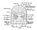
- FIG. 1A conventional light emitting diode, which uses a light emitting element and a phosphor to emit light of a desired color, is schematically shown in FIG. 1 .
- This light emitting diodeincludes a pair of lead frames 102 , 103 .
- the lead frame 102has a concave part in its leading end.
- a light emitting element 101is mounted on the bottom of the concave part.
- the light emitting element 101is covered with a phosphor-mixed resin 104 . Further, the space within of the concave part is filled with the phosphor-mixed resin 104 .
- the phosphor-mixed resin 104is a resin, such as a transparent epoxy resin, into which a phosphor has been mixed. This phosphor absorbs light emitted from the light emitting element 101 , performs wavelength conversion of the absorbed light, and gives off light with a wavelength different from the absorbed light.
- the whole assemblyhas been sealed with a sealing resin
- the light emitting diode having the above constructionassuming that, for example, the light emitting element 101 is a blue light emitting element and the phosphor is one which absorbs blue light emitted from the blue light emitting element, performs wavelength conversion of the blue light and gives off yellow light, the blue light emitted from the blue light emitting element is mixed with the yellow light given off from the phosphor. Therefore, theoretically, white light can be radiated to the outside of the light emitting diode as viewed from an emission observing surface of the light emitting diode.
- This light emitting diodesuffers from a problem that, as viewed from the emission observing surface of the light emitting diode, color of light radiated from the light emitting diode varies from position to position of the emission observing surface of the light emitting diode.
- the above unfavorable phenomenonwill be hereinafter referred to as “lack of uniformity of color of radiated light.”
- This problemis attributable to the following fact.
- a part of lightis radiated from the light emitting element 101 in a direction just above the light emitting element 101 .
- Another part of lightis radiated obliquely from the top surface or side surface of the light emitting element 101 .
- the amount of the phosphor, in the phosphor-mixed resin 104 , through which the light is passed in a period between the emission of the light from the light emitting element and the emergence of the light from the light emitting diodevaries depending upon optical paths through which the light is passed and radiated to the outside of the light emitting diode.
- This variation in the amount of phosphorwill be hereinafter often referred to as “a difference in the amount of light-permeated phosphor among the optical paths.”
- the emission observing surface in its portion just above the light emitting element 101is perceived as emitting white light, and a portion around that portion just above the light emitting element 101 is perceived as emitting yellow light.
- the light radiated from the light emitting diodelacks in uniformity of color.
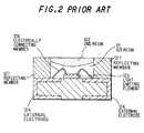
- Japanese Patent No. 3065263proposes a light emitting diode which reduces the lack of uniformity of color of radiated light.
- This light emitting diodeis shown in FIG. 2 .
- the light emitting diodeincludes a reflecting member 127 having a concave part.
- a light emitting element 123is mounted on the bottom of the concave part.
- the light emitting element 123is provided with a pair of electrodes (not shown). These electrodes are bonded respectively to external electrodes 124 through electrically connecting members 126 .
- the light emitting element 123 and the electrically connecting members 126are covered with and are embedded in a first resin 121 .
- the first resin 121is in a concave spherical surface as viewed from an emission observing surface of the light emitting diode.
- the remaining space, on the first resin 121 , of the concave partis filled with a second resin 122 which is a phosphor-mixed resin.
- the claimed advantage of this constructionis to substantially reduce the difference in the amount of light-permeated phosphor among the optical paths, and thus to reduce the lack of uniformity of color of light radiated from the light emitting diode.
- the thickness of the phosphor-containing second resin 122is the largest in a portion just above the light emitting element 123 and gradually decreases toward the side wall of the concave part.
- a part of light emitted from the light emitting element 123is radiated in a direction just above the light emitting element 123 to the outside of the light emitting diode through the second resin 122 in its large thickness portion.
- another part of light emitted from the light emitting element 123advances toward the inner wall of the reflecting member 127 , is reflected from the side wall of the concave part, and advances toward the outside of the light emitting diode through the second resin 122 in its small thickness portion.
- the amount of light-permeated phosphoris smaller than that in the emitted light passed through the other optical paths. That is, a difference in the amount of light-permeated phosphor among optical paths exists, and, thus, the light radiated from the light emitting diode lacks in uniformity of color. In other words, also in the above light emitting diode, light radiated from the light emitting diode disadvantageously lacks in uniformity of color as viewed from the emission observing surface of the light emitting diode.
- the inventionhas been made, and it is an object of the invention to provide a light emitting diode which can eliminate the problem of lack of uniformity of color of radiated light involved in the prior art and can radiate light having a desired uniform color as viewed from an emission observing surface of the light emitting diode.
- a light emitting diodecomprises: a reflecting mirror having a concave part; a light emitting element disposed within the concave part of the reflecting mirror; a light transparent layer formed of a first light transparent material which has been filled into a space within the concave part of the reflecting mirror so as to cover the light emitting element; and a fluorescence emitting layer provided on the light transparent layer on its emission observing surface side, said fluorescence emitting layer being formed of a second light transparent material which is different from the first light transparent material, said second transparent material containing a phosphor material that absorbs light which has been passed through the light transparent layer and emits light with a wavelength different from the absorbed light.
- the first light transparent materialis different from the second light transparent material, light is irregularly reflected from the interface of the first light transparent material and the second light transparent material, because the refractive index of the first light transparent material is different from that of the second transparent material.
- the probability of incidence of light having high optical density, which has been emitted from the light emitting element, directly to the phosphor material contained in the fluorescence emitting layeris lowered, and, instead, the probability of incidence of this light in a dispersed state to the phosphor material contained in the fluorescence emitting layer is increased.
- the lightcan be introduced in various directions from the light transparent layer into the fluorescence emitting layer to enhance the emission efficiency of the whole fluorescence emitting layer, and light having a uniform color can be radiated from the light emitting diode as viewed from the emission observing surface of the light emitting diode.
- a light emitting diodecomprises: a reflecting mirror having a concave part; a light emitting element disposed within the concave part of the reflecting mirror; a first layer formed of a phosphor material-containing light transparent material which has been filled into a space within the concave part of the reflecting mirror to the level of the upper surface of the light emitting element disposed within the concave part of the reflecting mirror; and a second layer formed of a phosphor material-containing light transparent material which is provided on the first layer on its emission observing surface side, said phosphor material contained in the first and second layers being capable of absorbing light emitted from the light emitting element and emitting light with a wavelength different from the absorbed light, the concentration of the phosphor in the second layer being higher than the concentration of the phosphor in the first layer.
- lights emitted in various directions from the light emitting elementare substantially equal to one another in the amount of phosphor through which the lights are passed in a period between the emission from the light emitting element and the radiation from the light emitting diode after passage through the first and the second layers. Therefore, during passage through the first and second layers, light given off from the phosphor after wavelength conversion can be uniformly mixed with light not passed through the phosphor, and, thus, light having a desired color can be uniformly radiated from the light emitting diode as viewed from an emission observing surface of the light emitting diode.
- a light emitting diodecomprises: a reflecting mirror having a concave part; a light emitting element disposed within the concave part of the reflecting mirror; and a phosphor material-containing light transparent material layer which has been filled into a space within the concave part of the reflecting mirror so as to cover the light emitting element, said phosphor material being capable of absorbing light emitted from the light emitting element and emitting light with a wavelength different from the absorbed light, said phosphor material having been distributed in said light transparent material layer so that values obtained by multiplying the length of optical paths, through which lights emitted from the light emitting element are passed and reach the upper surface of the light transparent material layer, by the concentration of the phosphor material are substantially equal to one another.
- lights emitted in various directions from the light emitting elementare substantially equal to one another in the amount of phosphor through which the lights are passed in a period between the emission from the light emitting element and the radiation from the light emitting diode after passage through the light transparent material. Therefore, during passage through the light transparent material, light given off from the phosphor after wavelength conversion can be uniformly mixed with light not passed through the phosphor, and, thus, light having a desired color can be uniformly radiated from the light emitting diode as viewed from an emission observing surface of the light emitting diode.
- a light emitting diodecomprises: a reflecting mirror having a concave part; a light emitting element disposed within the concave part of the reflecting mirror; a transparent light guiding/scattering layer which has been filled into a space within the concave part of the reflecting mirror so as to cover the light emitting element, said transparent light guiding/scattering layer being capable of scattering in various directions light emitted from the light emitting element; and a phosphor material-containing transparent fluorescence emitting layer which is provided on the light guiding/scattering layer in its emission observing surface side, said phosphor material being capable of absorbing light, which has been emitted from the light emitting element and passed through the light guiding/scattering layer, and capable of emitting light with a wavelength different from the absorbed light.
- the probability of incidence of light having high optical density, which has been emitted from the light emitting element, directly to the phosphor material contained in the fluorescence emitting layeris lowered, and, instead, the probability of incidence of this light in a dispersed state to the phosphor material contained in the fluorescence emitting layer is increased. Therefore, the light can be introduced in various directions from the light guiding/scattering layer into the fluorescence emitting layer to enhance the emission efficiency of the whole fluorescence emitting layer, and light having a desired uniform color can be radiated from the light emitting diode as viewed from the emission observing surface of the light emitting diode.
- FIG. 1is a cross-sectional view of an example of a conventional light emitting diode which utilizes a light emitting element and a phosphor to radiate light having a desired color;
- FIG. 2is a cross-sectional view of another example of a conventional light emitting diode which utilizes a light emitting element and a phosphor to radiate light having a desired color;
- FIG. 3Ais a cross-sectional view showing the construction of a light emitting diode in a first preferred embodiment of the invention
- FIG. 3Bis a diagram illustrating optical path lengths of lights emitted from a light emitting element used in the light emitting diode shown in FIG. 3A;
- FIG. 4is a diagram showing the layer construction of a blue light emitting element used in the light emitting diode in the first preferred embodiment of the invention
- FIG. 5is a cross-sectional view showing the construction of a light emitting diode in a second preferred embodiment of the invention.
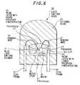
- FIG. 6is a cross-sectional view showing the construction of a light emitting diode in a third preferred embodiment of the invention.
- FIG. 7is a schematic cross-sectional view showing the construction of a light emitting diode in a fourth preferred embodiment of the invention.
- FIG. 8is a schematic cross-sectional view showing the construction of a light emitting diode in a fifth preferred embodiment of the invention.
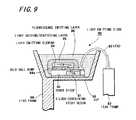
- FIG. 9is a schematic cross-sectional view showing the construction of a light emitting diode in a sixth preferred embodiment of the invention.
- FIG. 3Ais a cross-sectional view showing the construction of a light emitting diode in a first preferred embodiment of the invention.
- a light emitting diode 10 shown in this drawingis of shell type and includes two lead frames 12 , 13 which are electrically insulated from each other.
- a metal stem 14 provided with a concave cup 12 ais provided at the leading end of the lead frame 12 .
- the inner wall surface of the cup 12 afunctions as a reflecting mirror which reflects light.
- a flip chip-type light emitting elementis mounted on the bottom of the cup 12 a .
- the flip chip-type light emitting elementcomprises a blue light emitting element 17 which has been flip chip mounted onto an overvoltage protecting element 16 . More specifically, the overvoltage protecting element 16 is fixed onto the bottom of the cup 12 a through a mount 18 of a conductive paste.
- a blue light emitting element 17which emits blue light with a wavelength of 450 to 550 nm, has been flip chip mounted on the overvoltage protecting element 16 .
- the layer construction of the blue light emitting element 17is shown in FIG. 4 .
- a sapphire substrate 17 ais provided as a transparent substrate.
- a buffer layer 17 ban n-type contact layer 17 c , an n-type cladding layer 17 d , a layer 17 e including a light emitting layer, a p-type cladding layer 17 f , and a p-type contact layer 17 g are formed as nitride semiconductor layers, for example, by MOCVD (metal-organics chemical vapor deposition) in that order on the sapphire substrate 17 a .
- MOCVDmetal-organics chemical vapor deposition
- a light nontransparent and light reflecting electrode 17 his formed on the whole surface of the p-type contact layer 17 g , a p electrode 17 i is formed on a part of the light nontransparent and light reflecting electrode 17 h , and an n electrode 17 j is formed on a part of the n-type contact layer 17 c.
- the flip chip mounting of this blue light emitting element 17is carried out as follows. As shown in FIG. 3A, the lower surface of the sapphire substrate 17 a shown in FIG. 4 is provided as the uppermost surface.
- the p electrode 17 i in the blue light emitting element 17 shown in FIG. 4is connected to an electrode 16 a on an n layer in the overvoltage protecting element 16 through a gold bump 19 .
- the n electrode 17 jis connected to an electrode 16 b on a p layer in the overvoltage protecting element 16 through a gold bump 20 .
- the electrode 16 b in the overvoltage protecting element 16is connected to the lead frame 13 through a bonding wire 22 .
- a resin layer 24 with a lower phosphor concentrationwhich will be explained later, is filled into the space within the cup 12 a to the level of the uppermost surface of the blue light emitting element 17 .
- a resin layer 25 with a higher phosphor concentrationis provided on the resin layer 24 with a lower phosphor concentration to such a level that, in the cross section, the center portion is bulged from the top level of the cup 12 a . More specifically, as viewed from above the top of the blue light emitting element 17 , the resin layer 24 with a lower phosphor concentration is provided in a ring form around the uppermost surface of the blue light emitting element 17 .
- the upper surface of the resin layer 24 with a lower phosphor concentration on both sides of the blue light emitting element 17is in an arcuately concaved form.
- the upper surface of the resin layer 25 with a higher phosphor concentrationis in such a convex form that the portion just above the blue light emitting element 17 is bulged on the highest level.
- the whole assemblyhas been sealed with an external resin 29 to form a shell-shaped light emitting diode 10 .
- the resin layer 24 with a lower phosphor concentrationis formed of a light transparent resin, such as an epoxy resin or a silicone resin, into which a phosphor 27 , which absorbs blue light emitted from the blue light emitting element 17 and emits yellow light, has been mixed in a lower concentration than that in the resin layer 25 .
- the resin layer 25 with a higher phosphor concentrationis formed of a light transparent resin into which the phosphor 27 has been mixed in a higher phosphor concentration than that in the resin layer 24 .
- the phosphor 27may be a Ce:YAG (yttrium-aluminum-garnet) phosphor.
- Examples of additional phosphor materials usable hereininclude rare earth phosphors, such as yttrium (Y), gadolinium (Gd), and cerium (Ce), inorganic phosphors, organic phosphors, fluorescent dyes, and fluorescent pigments.
- rare earth phosphorssuch as yttrium (Y), gadolinium (Gd), and cerium (Ce)
- inorganic phosphorssuch as yttrium (Y), gadolinium (Gd), and cerium (Ce)
- inorganic phosphorssuch as yttrium (Y), gadolinium (Gd), and cerium (Ce)
- organic phosphorssuch as organic phosphors, fluorescent dyes, and fluorescent pigments.
- the concentration of the phosphor 27 in the layers 24 , 25 or the form of the layers 24 , 25has been regulated so that values obtained by multiplying the lengths of optical paths, through which lights emitted from the blue light emitting element 17 reach the interface of the resin layer 25 with a higher phosphor concentration and the external resin 29 , by the concentration of the phosphor 27 are substantially equal to one another.
- FIG. 3Billustrating the length of optical paths of lights emitted from the light emitting element.
- multiplication values A′, B′, and C′are substantially equal to one another, wherein A′ represents the multiplication value obtained by multiplying the length of the optical path A by the concentration of the phosphor 27 , B′ represents the multiplication value obtained by multiplying the length of the optical path B by the concentration of the phosphor 27 , and C′ represents the multiplication value obtained by multiplying the length of the optical path C by the concentration of the phosphor 27 .
- A′represents the multiplication value obtained by multiplying the length of the optical path A by the concentration of the phosphor 27
- B′represents the multiplication value obtained by multiplying the length of the optical path B by the concentration of the phosphor 27
- C′represents the multiplication value obtained by multiplying the length of the optical path C by the concentration of the phosphor 27 .
- l 1 to l 9each represent an optical path length
- d 1represents a high concentration
- d 2represents a low concentration
- C 1represents an arc part
- C 2represents a convex part.
- A′l 1 ⁇ d 1
- B′(l 2 +l 3 )d 2 +l 4 ⁇ d 1 .
- C′(l 5 +l 7 +l 8 )d 2 +(l 6 +l 9 )d 1 .
- the relationship among A′, B′, and C′is A′ ⁇ B′ ⁇ C′.
- the resin, into which the phosphor 27 has been mixedmay be prepared, for example, by mixing a main agent as a light transparent resin and a curing agent together at a predetermined ratio, stirring and defoaming the mixture, mixing the resin with Aerosil and a silane coupling agent together, and thoroughly kneading the mixture.
- a main agentas a light transparent resin and a curing agent together at a predetermined ratio
- stirring and defoaming the mixturemixing the resin with Aerosil and a silane coupling agent together
- thoroughly kneading the mixtureAn embodiment, wherein this resin is used for the formation of the layers 24 , 25 , will be explained.
- the concentration of the phosphor 27 in the resin layer 24 with a lower phosphor concentrationis brought to 20% while the concentration of the phosphor 27 in the resin layer 25 with a higher phosphor concentration is brought to 60%.
- curingis carried out at 120° C. for one hr.
- the blue light emitting element 17upon the application of voltage to the lead frames 12 , 13 , the blue light emitting element 17 emits blue light.
- blue light which is emitted in a direction just above the blue light emitting element 17is different from blue light which is emitted obliquely from the upper surface or side face of the blue light emitting element 17 or blue light which, after emission from the blue light emitting element 17 , is reflected from the inner wall of the cup 12 a , in the length of optical path through the light is passed through the layers 24 , 25 .
- the concentration of the phosphor 27 in the layers 24 , 25 or the form of the layers 24 , 25has been regulated so that values obtained by multiplying the length of optical paths by the concentration of the phosphor 27 are substantially equal to one another. Therefore, lights emitted in the above respective directions from the blue light emitting element 17 are substantially equal to one another in the amount of phosphor 27 through which the light is passed in a period between the emission from the blue light emitting element 17 and the entry of the external resin 29 after the passage through the layers 24 , 25 .
- the optical paths A, B, and Care substantially equal to one another in the amount of light-permeated phosphor 27 .
- the light emitted from the blue light emitting element 17is subjected to wavelength conversion in the phosphor 27 which emits yellow light.
- the yellow lightis mixed with blue light, which is emitted from the blue light emitting element 17 but not passed through the phosphor 27 . Therefore, the radiation of uniform white light from the light emitting diode 10 can be realized as viewed from the emission observing surface of the light emitting diode 10 .
- the light nontransparent and light reflecting electrode 17 hhas been formed on the whole surface of the upper surface of the p-type contact layer 17 g in the blue light emitting element 17 .
- a light transparent electrodemay be used instead of the light nontransparent and light reflecting electrode 17 h.
- FIG. 5is a cross-sectional view showing the construction of a light emitting diode in a second preferred embodiment of the invention.
- FIG. 5 showing the light emitting diode in the second preferred embodiment and FIG. 3A showing the light emitting diode in the first preferred embodimentlike parts are identified with the same reference numerals, and the overlapped explanation thereof will be omitted.
- a light emitting diode 40 shown in FIG. 5is different from the light emitting diode shown in FIG. 3A in that, instead of the flip chip-type light emitting element explained in the first preferred embodiment, a blue light emitting element 42 has been fixed onto the bottom of a cup 12 a through a mount 18 in a face-up manner.
- the blue light emitting element 42is the same as the blue light emitting element 17 shown in FIG. 4, except that a light reflecting film 42 a is additionally provided on the lower surface of the sapphire substrate 17 a .
- the p electrode 17 i of the blue light emitting element 42is connected through a bonding wire 21 to a lead frame 12
- the n electrode 17 j of the blue light emitting element 42is connected through a bonding wire 22 to a lead frame 13 .
- This blue light emitting element 42is configured so that light, which has been emitted in a direction just below the blue light emitting element 42 is reflected from the reflecting film 42 a and is radiated in a direction just above the light emitting element 42 .
- a resin layer 24 with a lower phosphor concentrationis filled into the space within the cup 12 a to the level of the uppermost surface of the blue light emitting element 42 , and a resin layer 25 with a higher phosphor concentration is provided on the resin layer 24 with a lower phosphor concentration so that, as viewed in the cross section, the center portion of the resin layer 25 with a higher phosphor concentration just above the blue light emitting element 42 is bulged from the top level of the cup 12 a .
- the concentration of the phosphor 27 in the layers 24 , 25 and the form of the layers 24 , 25have been regulated so that values obtained by multiplying the lengths of optical paths, through which lights emitted from the blue light emitting element 42 reach the interface of the resin layer 25 with a higher phosphor concentration and the external resin 29 , by the concentration of the phosphor 27 are substantially equal to one another.
- the light emitting diode 40 having the above constructioncan also attain the same effect as in the light emitting diode 10 in the first preferred embodiment.
- FIG. 6is a cross-sectional view showing the construction of a light emitting diode in a third preferred embodiment of the invention.
- FIG. 6showing the light emitting diode in the third preferred embodiment
- FIG. 5showing the light emitting diode in the second preferred embodiment
- like partsare identified with the same reference characters, and the overlapped explanation thereof will be omitted.
- a light emitting diode 50 shown in FIG. 6is different from the light emitting diode shown in FIG. 5 in that, instead of the blue light emitting element 42 explained above in the second preferred embodiment, a blue light emitting element 17 as shown in FIG. 4 has been fixed onto the bottom of a cup 12 a through a mount 18 .
- the mount 18contains a silver (Ag) filler and a phosphor 27 .
- a silver (Ag) fillerand a phosphor 27 .
- blue lightwhich has been emitted in a direction just below the blue light emitting element 17 , is subjected to wavelength conversion by the phosphor 27 , contained in the mount 18 , which emits yellow light.
- the yellow lightis reflected from the bottom of the cup 12 a in a direction just above the mount 18 or in an oblique direction.
- the light emitting diode in conjunction with this preferred embodimentcan attain the same effect as the light emitting diode in the second preferred embodiment and further can attain the following additional effect. Specifically, blue light emitted in a direction just below the blue light emitting element 17 is once subjected to wavelength conversion by the phosphor 27 , contained in the mount 18 , which gives off yellow light. The yellow light is then reflected from the bottom of the cup 12 a in a direction just above the mount 18 or in an oblique direction.
- the necessary quantity of light to be subjected to wavelength conversion in the phosphor contained in the resin layer 25 with a higher phosphor concentrationcan be reduced by the quantity of light subjected to wavelength conversion in the phosphor 27 contained in the mount 18 , and, thus, the thickness of the resin layer 25 with a higher phosphor concentration can be reduced.
- the reduction in the thickness of the resin layer 25 with a higher phosphor concentrationcan realize a further reduction in thickness of light emitting diodes, particularly SMD-type light emitting diodes.
- the incorporation of a reflecting agent, such as spherical glass beads, into the resin layer 24 with a lower phosphor concentrationcauses irregular reflection of light which can maintain uniformity of light.
- the resin layerhas been divided into two layers, the resin layer 24 with a lower phosphor concentration and the resin layer 25 with a higher phosphor concentration.
- a constructionmay be adopted wherein the space within the cup 12 a is filled with a single-layer light transparent resin of which the concentration of the phosphor 27 has been gradually changed so that values obtained by multiplying the length of optical paths by the concentration of the phosphor 27 are substantially equal to one another.
- a blue light emitting elementhas been used as a light emitting element.
- the light emitting elementis not limited to the blue light emitting element and may be any light emitting element including ultraviolet light emitting elements so far as the light emitting element emits light with a wavelength which can excite the phosphor.
- a transparent epoxy resinhas been used as the light transparent material for sealing the light emitting element and the like.
- other materials including transparent silicone resinsmay also be used.
- FIG. 7is a schematic cross-sectional view showing the construction of a light emitting diode in a fourth preferred embodiment of the invention.
- a light emitting diode 60 in this preferred embodimentincludes a lead frame 68 .
- a concave cup 69is provided at the leading end of the lead frame 68 .
- a light emitting element 61is provided within the cup 69 so that light emitted from the light emitting element 61 can be radiated in a direction above the cup 69 .
- the light emitting element 61may be any light emitting element which can emit light with any wavelength in a region from the infrared to the ultraviolet.
- a light emitting elementwhich emits light in an ultraviolet region or in a near-ultraviolet region, is suitable because light emitted from the light emitting element can be efficiently converted to contemplated light without the perception of the light emitted by the light emitting element 61 directly by a viewer.
- the results of experiments conducted by the present inventorsshow that, when a near-ultraviolet light emitting element is used as the light emitting element 61 to emit near-ultraviolet light which excites a phosphor material 65 described later, due to relatively short wavelength, energy can be relatively strongly excited, contributing to enhanced emission efficiency.
- a gallium nitride compound semiconductor material having an emission wavelength band in the range of 360 to 390 nm not harmful to the human bodymay be used in the near-ultraviolet light emitting element 61 .
- the light emitting element 61is electrically connected to the cup 69 through a lead wire (not shown).
- a transparent binderis coated onto the periphery of the light emitting element 61 to form an inner resin layer 62 .
- the inner resin layer 62is formed of a material having high adhesion to the light emitting element 61 , such as an epoxy resin, an acrylic resin, a urea resin, or a silicone resin.
- the thickness of the inner resin layer 62is generally not less than several tens of micrometers. The thickness of the inner resin layer 62 , however, may be properly determined by taking into consideration factors such as the number of layers constituting the inner resin layer and the refractive index of the material constituting the layer.
- an outer resin layer 63is provided on the outer periphery of the inner resin layer 62 .
- the outer resin layer 63is formed of a material having a refractive index different from the inner resin layer 62 .
- the outer resin layer 63is provided within the cup 69 so as to fill up the space defined by the inner wall of the cup 69 and the light emitting element 61 with the inner resin layer 62 formed thereon and to cover the light emitting element 61 with the inner resin layer 62 formed thereon.
- the outer resin layer 63may also be formed of a material such as an epoxy resin, an acrylic resin, a urea resin, or a silicone resin.
- the thickness of the light guiding/scattering layer 64may be 50 to 300 ⁇ m.
- the inner resin layer 62is formed of a material which is different from the outer resin layer 63 .
- the light guiding/scattering layer 64may have a multilayer structure of more than two layers or may be formed of a material having a relatively high refractive index.
- the light emitting diodemay take the form of a shell-shaped light emitting diode in which the periphery of the light emitting element has been molded with a resin to form a lens part in the shell-shaped light emitting diode.
- the whole or a part of the resin used in the formation of the shell-shaped light emitting diodemay constitute the light guiding/scattering layer or one of the layers constituting the light guiding/scattering layer.
- the fluorescence emitting layer 67is formed of a transparent binder 66 containing a phosphor material 65 which gives off light having a desired color.
- Rare earth phosphorssuch as yttrium (Y), gadolinium (Gd), and cerium (Ce) may be used as the phosphor material 65 .
- Examples of other phosphor materials usable hereininclude inorganic phosphors, organic phosphors, fluorescent dyes, and fluorescent pigments.
- the fluorescence emitting layer 67may be formed of a material prepared by mixing and kneading a fine powder of the phosphor material 65 and a transparent binder, such as an epoxy resin, an acrylic resin, a urea resin, or a silicone resin, together.
- the thickness of the fluorescence emitting layer 67may also be 10 to 300 ⁇ m.
- the phosphor material 65may be mixed into the transparent binder 66 to a concentration of 2 to 20% by volume based on the transparent binder 66 .
- the fluorescence emitting layer 67When the concentration of the phosphor material 65 in the transparent binder 66 is low, the fluorescence emitting layer 67 is formed in a large thickness, while when the concentration of the phosphor material 65 in the transparent binder 66 is high, the fluorescence emitting layer 67 is formed in a small thickness.
- the light emitting diode 60 in this preferred embodimentin the light guiding/scattering layer 64 , light, which has been emitted from the light emitting element 61 and has entered the inner resin layer 62 , is reflected from and is scattered at the interfacial boundary between the inner resin layer 62 and the outer resin layer 63 with high probability and is led to the fluorescence emitting layer 67 . Therefore, the probability of incidence of light having high optical density, which has been emitted from the light emitting element 61 , directly to the phosphor material 65 contained in the fluorescence emitting layer 67 is lowered, and the probability of incidence of this light in a dispersed state to the phosphor material 65 contained in the fluorescence emitting layer 67 is increased.
- the lightcan be introduced in various directions from the light guiding/scattering layer 64 into the fluorescence emitting layer 67 to enhance the emission efficiency of the whole fluorescence emitting layer 67 , and light having a desired uniform color can be radiated from the light emitting diode as viewed from the emission observing surface of the light emitting diode.
- the light guiding/scattering layer 64has a two-layer structure.
- the number of layers constituting the light guiding/scattering layer 64may be increased to improve light scattering efficiency. In this case, however, the number of layers constituting the light guiding/scattering layer 64 is preferably two to five from the viewpoint of cost effectiveness.
- any phosphor materialis not contained in the light guiding/scattering layer 64 .
- a suitable amount of a phosphor materialmay also be contained in the light guiding/scattering layer 64 .
- FIG. 8is a schematic cross-sectional view showing the construction of a light emitting diode in a fifth preferred embodiment of the invention.
- FIG. 8showing the light emitting diode in the fifth preferred embodiment of the invention
- FIG. 7showing the light emitting diode in the fourth preferred embodiment of the invention
- like partsare identified with the same reference numerals, and the overlapped explanation thereof will be omitted.
- a light guiding/scattering layer 64 formed of a transparent binder 73 with a light scattering material 72 incorporated thereinis formed on the periphery of the light emitting element 61 as shown in FIG. 7 (fourth preferred embodiment).
- the light scattering material 72 for scattering the incident lightmay be a member selected from the group consisting of aluminum oxide, titanium oxide, barium titanate, and silicon oxide, or a combination of two or more of them.
- a material having high adhesion to the light emitting element 61is selected as the transparent binder 73 .
- materials usable as the transparent binder 73include synthetic resins, such as epoxy resins, acrylic resins, urea resins, and silicone resins, and synthetic rubbers.
- the light guiding/scattering layer 64may be formed by mixing and kneading the transparent binder 73 and the scattering material 72 together and pouring the kneaded mixture into a space around the light emitting element 61 disposed within the cup 69 .
- the thickness of the light guiding/scattering layer 64may be properly determined depending upon the content of the scattering material 72 in the light guiding/scattering layer 64 .
- the light guiding/scattering layer 64is provided, on the light emitting element 61 , in an arc form or a convex lens form, that is, in such a manner that the thickness of the center portion is larger and the thickness of the peripheral portion is smaller.
- the reason for the adoption of this form of the light guiding/scattering layeris as follows.
- the upper surface of the light guiding/scattering layer 64may be made on a level which is parallel to the opening of the cup 69 (horizontal surface).
- the thickness of the light guiding/scattering layer 64may be 50 to 300 ⁇ m.
- a fluorescence emitting layer 67is provided on the upper surface of the light guiding/scattering layer 64 .
- the light scattering material 72 contained in the light guiding/scattering layer 64can irregularly reflect and scatter the incident light in various directions and can guide the scattered light to the fluorescence emitting layer 67 . Therefore, as with the fourth preferred embodiment, by virtue of the provision of the light guiding/scattering layer 64 , the probability of incidence of light having high optical density, which has been emitted from the light emitting element 61 , directly to the phosphor material 65 contained in the fluorescence emitting layer 67 is lowered, and the probability of incidence of this light in a dispersed state to the phosphor material 65 contained in the fluorescence emitting layer 67 is increased.
- the lightcan be introduced in various directions from the light guiding/scattering layer 64 into the fluorescence emitting layer 67 to enhance the emission efficiency of the whole fluorescence emitting layer 67 , and light having a desired uniform color can be radiated from the light emitting diode as viewed from the emission observing surface of the light emitting diode.
- FIG. 9is a schematic cross-sectional view showing the construction of a light emitting diode in a sixth preferred embodiment of the invention.
- FIG. 9showing the light emitting diode in the sixth preferred embodiment of the invention
- FIGS. 7 and 8showing the light emitting diodes in the fourth and fifth preferred embodiments of the invention
- like partsare identified with the same reference numerals, and the overlapped explanation thereof will be omitted.
- a light emitting element 84 having a flip chip structureis used.
- the light emitting element 84is connected in parallel to the upper surface of a Zener diode 80 through a gold ball bump 84 a .
- the Zener diode 80is disposed in the inner surface of a concave cup provided at the leading end of the lead frame 68 through an electrically conductive silver-mixed epoxy resin 81 . Accordingly, the Zener diode 80 is electrically and mechanically connected to the cup 69 in the lead frame 68 .
- the other end of the Zener diode 80is connected to a lead frame 82 through a lead 83 . That is, the light emitting element 84 is disposed within the cup 69 so that light emitted from the light emitting element 84 is radiated on the Zener diode 80 side and in a direction above the cup 69 .
- a light guiding/scattering layer 85 formed of a transparent binder (which is the same as the transparent binder 73 shown in FIG. 8) with a light scattering material (which is the same as the light scattering material 72 shown in FIG. 8) for guiding and scattering lightis provided on the periphery of the light emitting element 84 .
- the light guiding/scattering layer 85is also provided between the Zener diode 80 and the light emitting element 84 .
- a material, which can scatter light in a transparent synthetic resin material or a transparent synthetic rubber material,may also be used as the light scattering material.
- the light scattering materialmay of course be either partially permeable to light or fully reflect light.
- the concentration of the light scattering material in the light guiding/scattering layer 85is suitably in the range of 2 to 20% by volume based on the transparent binder. However, the concentration of the light scattering material in the light guiding/scattering layer 85 as well as the thickness of the light guiding/scattering layer 85 may be properly regulated.
- the thickness of the light guiding/scattering layer 85is preferably 50 to 300 ⁇ m from the viewpoint of the contemplated effect.
- a fluorescence emitting layer 86is provided on the light guiding/scattering layer 85 .
- the fluorescence emitting layer 86is formed of a transparent binder (which is the same as the transparent binder 66 shown in FIG. 8) with a phosphor material (which is the same as the phosphor material 65 shown in FIG. 8) capable of giving off a predetermined color mixed thereinto.
- the phosphor material, the transparent binder, and the fluorescence emitting layermay be the same as those in the fourth and fifth preferred embodiments.
- the light guiding/scattering layer 85can irregularly reflect and scatter the incident light in various directions and can guide the scattered light to the fluorescence emitting layer 86 . Therefore, the probability of incidence of light having high optical density, which has been emitted from the light emitting element 84 , directly to the fluorescence emitting layer 86 is lowered, and light in a dispersed state is incident to the fluorescence emitting layer 86 .
- the light emitting element 84 usedhas a flip chip structure. Therefore, light emitted upward from the light emitting element 84 is radiated directly upward through the substrate. On the other hand, light radiated downward from the light emitting element 84 is reflected from the upper surface of the Zener diode 80 and is guided upward. Therefore, the density of emitted light can be further homogenized in the light guiding/scattering layer 85 , and the light is then radiated upward through the opening of the cup 69 . Therefore, the brightness of light radiated from the light guiding/scattering layer 85 can be further enhanced.
Landscapes
- Led Device Packages (AREA)
Abstract
Description
Claims (15)
Applications Claiming Priority (4)
| Application Number | Priority Date | Filing Date | Title |
|---|---|---|---|
| JP2002128790AJP2003324215A (en) | 2002-04-30 | 2002-04-30 | Light emitting diode lamp |
| JP2002-128790 | 2002-04-30 | ||
| JP2002-276184 | 2002-09-20 | ||
| JP2002276184AJP2004111882A (en) | 2002-09-20 | 2002-09-20 | Light emitting device |
Publications (2)
| Publication Number | Publication Date |
|---|---|
| US20030214233A1 US20030214233A1 (en) | 2003-11-20 |
| US6791116B2true US6791116B2 (en) | 2004-09-14 |
Family
ID=29272389
Family Applications (1)
| Application Number | Title | Priority Date | Filing Date |
|---|---|---|---|
| US10/424,137Expired - LifetimeUS6791116B2 (en) | 2002-04-30 | 2003-04-28 | Light emitting diode |
Country Status (4)
| Country | Link |
|---|---|
| US (1) | US6791116B2 (en) |
| KR (2) | KR100617432B1 (en) |
| CN (1) | CN1455462A (en) |
| TW (1) | TW595018B (en) |
Cited By (73)
| Publication number | Priority date | Publication date | Assignee | Title |
|---|---|---|---|---|
| US20050077535A1 (en)* | 2003-10-08 | 2005-04-14 | Joinscan Electronics Co., Ltd | LED and its manufacturing process |
| US20050221519A1 (en)* | 2004-03-31 | 2005-10-06 | Michael Leung | Semiconductor light emitting devices including a luminescent conversion element and methods for packaging the same |
| US20060061259A1 (en)* | 2004-09-23 | 2006-03-23 | Negley Gerald H | Semiconductor light emitting devices including patternable films comprising transparent silicone and phosphor, and methods of manufacturing same |
| US20060091415A1 (en)* | 2004-10-29 | 2006-05-04 | Ledengin, Inc. (Cayman) | LED package with structure and materials for high heat dissipation |
| US20060091788A1 (en)* | 2004-10-29 | 2006-05-04 | Ledengin, Inc. | Light emitting device with a thermal insulating and refractive index matching material |
| US20060094137A1 (en)* | 2004-10-29 | 2006-05-04 | Ledengin, Inc. (Cayman) | Method of manufacturing ceramic LED packages |
| US20060091416A1 (en)* | 2004-10-29 | 2006-05-04 | Ledengin, Inc. (Cayman) | High power LED package with universal bonding pads and interconnect arrangement |
| US20060208269A1 (en)* | 2005-03-18 | 2006-09-21 | Kim Bum J | Side-emitting LED package having scattering area and backlight apparatus incorporating the LED lens |
| US20070029926A1 (en)* | 2005-08-04 | 2007-02-08 | Taiwan Oasis Technology Co., Ltd. | Multi-wavelength LED construction & manufacturing process |
| US20070069633A1 (en)* | 2005-09-27 | 2007-03-29 | Sanyo Electric Co., Ltd. | Light emitting device and method for manufacturing the same |
| US7297988B2 (en) | 2005-04-15 | 2007-11-20 | Samsung Electro-Mechanics Co., Ltd. | Flip chip type nitride semiconductor light emitting device |
| US20080111147A1 (en)* | 2005-08-12 | 2008-05-15 | Avago Technologies Ecbu Ip (Singapore) Pte. Ltd. | Phosphor-Converted LED Devices Having Improved Light Distribution Uniformity |
| US20080128732A1 (en)* | 2006-10-26 | 2008-06-05 | Toyoda Gosei Co., Ltd. | Light emitting device |
| US20080210961A1 (en)* | 2007-03-03 | 2008-09-04 | Lite-On Technology Corp. | Light emitting device |
| US20080284315A1 (en)* | 2007-04-16 | 2008-11-20 | Toyoda Gosei, Ltd. | Light emitting device and light emitter |
| US20090001390A1 (en)* | 2007-06-29 | 2009-01-01 | Ledengin, Inc. | Matrix material including an embedded dispersion of beads for a light-emitting device |
| US20090039369A1 (en)* | 2007-08-07 | 2009-02-12 | Wakako Niino | Semiconductor light emitting apparatus |
| US20090159918A1 (en)* | 2003-12-09 | 2009-06-25 | Cree, Inc. | Semiconductor light emitting devices and submounts and methods for forming the same |
| US20090256167A1 (en)* | 2006-06-08 | 2009-10-15 | Koninklijke Philips Electronics N.V. | Light-emitting device |
| US20090315068A1 (en)* | 2008-06-18 | 2009-12-24 | Kabushiki Kaisha Toshiba | Light emitting device |
| US20090321770A1 (en)* | 2008-06-25 | 2009-12-31 | Shuichi Ajiki | Semiconductor Light-Emitting Device |
| US20100044735A1 (en)* | 2008-08-25 | 2010-02-25 | Citizen Electronics Co., Ltd. | Light-emitting device |
| US20100081218A1 (en)* | 2008-09-26 | 2010-04-01 | Craig Hardin | Forming Light Emitting Devices Including Custom Wavelength Conversion Structures |
| US20100091499A1 (en)* | 2008-10-14 | 2010-04-15 | Ledengin, Inc. | Total Internal Reflection Lens and Mechanical Retention and Locating Device |
| US20100117106A1 (en)* | 2008-11-07 | 2010-05-13 | Ledengin, Inc. | Led with light-conversion layer |
| US20100155755A1 (en)* | 2008-12-24 | 2010-06-24 | Ledengin, Inc. | Light-emitting diode with light-conversion layer |
| US7772604B2 (en) | 2006-01-05 | 2010-08-10 | Illumitex | Separate optical device for directing light from an LED |
| US20100213487A1 (en)* | 2009-02-24 | 2010-08-26 | Advanced Optoelectronic Technology, Inc. | Side-emitting led package and manufacturing method of the same |
| US7789531B2 (en) | 2006-10-02 | 2010-09-07 | Illumitex, Inc. | LED system and method |
| US20100259924A1 (en)* | 2009-04-08 | 2010-10-14 | Ledengin, Inc. | Lighting Apparatus Having Multiple Light-Emitting Diodes With Individual Light-Conversion Layers |
| US7829358B2 (en) | 2008-02-08 | 2010-11-09 | Illumitex, Inc. | System and method for emitter layer shaping |
| US20100301357A1 (en)* | 2008-01-04 | 2010-12-02 | Wei-An Chen | Light emitting element |
| US20110140142A1 (en)* | 2007-07-06 | 2011-06-16 | Yu Ho Won | Light emitting device package |
| US20110149581A1 (en)* | 2009-12-17 | 2011-06-23 | Ledengin, Inc. | Total internal reflection lens with integrated lamp cover |
| US20110164203A1 (en)* | 2009-06-22 | 2011-07-07 | Panasonic Corporation | Surface light source and liquid crystal display apparatus |
| US20110193118A1 (en)* | 2010-02-09 | 2011-08-11 | Oshima Yukitoyo | Light emitting device and manufacturing method thereof |
| US8044412B2 (en) | 2006-01-20 | 2011-10-25 | Taiwan Semiconductor Manufacturing Company, Ltd | Package for a light emitting element |
| US20110309387A1 (en)* | 2010-06-21 | 2011-12-22 | Hon Hai Precision Industry Co., Ltd. | Light emitting diode and light module having same |
| US8115217B2 (en) | 2008-12-11 | 2012-02-14 | Illumitex, Inc. | Systems and methods for packaging light-emitting diode devices |
| US20120104957A1 (en)* | 2010-11-01 | 2012-05-03 | Citizen Holdings Co., Ltd. | Light-emitting device |
| US20120161181A1 (en)* | 2010-12-24 | 2012-06-28 | Yoo Cheol Jun | Light emitting device package and method of manufacturing the same |
| US20120236529A1 (en)* | 2011-03-15 | 2012-09-20 | Avago Technologies Ecbu Ip(Singapore) Pte. Ltd. | Method And Apparatus For A Light Source |
| US8384097B2 (en) | 2009-04-08 | 2013-02-26 | Ledengin, Inc. | Package for multiple light emitting diodes |
| US8449128B2 (en) | 2009-08-20 | 2013-05-28 | Illumitex, Inc. | System and method for a lens and phosphor layer |
| US8585253B2 (en) | 2009-08-20 | 2013-11-19 | Illumitex, Inc. | System and method for color mixing lens array |
| US8598793B2 (en) | 2011-05-12 | 2013-12-03 | Ledengin, Inc. | Tuning of emitter with multiple LEDs to a single color bin |
| US20140117388A1 (en)* | 2012-10-29 | 2014-05-01 | Advanced Semiconductor Engineering, Inc. | Light-emitting semiconductor packages and related methods |
| US8816369B2 (en) | 2004-10-29 | 2014-08-26 | Led Engin, Inc. | LED packages with mushroom shaped lenses and methods of manufacturing LED light-emitting devices |
| US8858022B2 (en) | 2011-05-05 | 2014-10-14 | Ledengin, Inc. | Spot TIR lens system for small high-power emitter |
| US20140328083A1 (en)* | 2011-11-17 | 2014-11-06 | Lumens Co., Ltd. | Light emitting device package and backlight unit comprising the same |
| US9041046B2 (en) | 2011-03-15 | 2015-05-26 | Avago Technologies General Ip (Singapore) Pte. Ltd. | Method and apparatus for a light source |
| US9080729B2 (en) | 2010-04-08 | 2015-07-14 | Ledengin, Inc. | Multiple-LED emitter for A-19 lamps |
| US20160005722A1 (en)* | 2013-02-22 | 2016-01-07 | Osram Opto Semiconductors Gmbh | Optoelectronic Semiconductor Component and Method for Producing Same |
| US9234801B2 (en) | 2013-03-15 | 2016-01-12 | Ledengin, Inc. | Manufacturing method for LED emitter with high color consistency |
| US9345095B2 (en) | 2010-04-08 | 2016-05-17 | Ledengin, Inc. | Tunable multi-LED emitter module |
| US20160172554A1 (en)* | 2013-07-19 | 2016-06-16 | Koninklijke Philips N.V. | Pc led with optical element and without ssubstrate carrier |
| US9406654B2 (en) | 2014-01-27 | 2016-08-02 | Ledengin, Inc. | Package for high-power LED devices |
| US20160336485A1 (en)* | 2014-02-06 | 2016-11-17 | Koninklijke Philips N.V. | Light emitting diode with structured substrate |
| US9528665B2 (en) | 2011-05-12 | 2016-12-27 | Ledengin, Inc. | Phosphors for warm white emitters |
| US9530943B2 (en) | 2015-02-27 | 2016-12-27 | Ledengin, Inc. | LED emitter packages with high CRI |
| US9642206B2 (en) | 2014-11-26 | 2017-05-02 | Ledengin, Inc. | Compact emitter for warm dimming and color tunable lamp |
| RU2639565C2 (en)* | 2012-03-30 | 2017-12-21 | Люмиледс Холдинг Б.В. | Light-emitting device with wavelength-converting side coating |
| US9897284B2 (en) | 2012-03-28 | 2018-02-20 | Ledengin, Inc. | LED-based MR16 replacement lamp |
| US9929326B2 (en) | 2004-10-29 | 2018-03-27 | Ledengin, Inc. | LED package having mushroom-shaped lens with volume diffuser |
| US10219345B2 (en) | 2016-11-10 | 2019-02-26 | Ledengin, Inc. | Tunable LED emitter with continuous spectrum |
| US10381538B2 (en)* | 2017-01-24 | 2019-08-13 | Nichia Corporation | Light emitting device having fluorescent and light scattering light-transmissive member |
| US10575374B2 (en) | 2018-03-09 | 2020-02-25 | Ledengin, Inc. | Package for flip-chip LEDs with close spacing of LED chips |
| US10593854B1 (en) | 2006-12-11 | 2020-03-17 | The Regents Of The University Of California | Transparent light emitting device with light emitting diodes |
| US11032884B2 (en) | 2012-03-02 | 2021-06-08 | Ledengin, Inc. | Method for making tunable multi-led emitter module |
| US11313671B2 (en) | 2019-05-28 | 2022-04-26 | Mitutoyo Corporation | Chromatic confocal range sensing system with enhanced spectrum light source configuration |
| US11592166B2 (en) | 2020-05-12 | 2023-02-28 | Feit Electric Company, Inc. | Light emitting device having improved illumination and manufacturing flexibility |
| US11876042B2 (en) | 2020-08-03 | 2024-01-16 | Feit Electric Company, Inc. | Omnidirectional flexible light emitting device |
| EP4456159A1 (en)* | 2023-04-25 | 2024-10-30 | Seoul Semiconductor Co., Ltd. | Light emitting device |
Families Citing this family (82)
| Publication number | Priority date | Publication date | Assignee | Title |
|---|---|---|---|---|
| US20070164661A1 (en)* | 1999-07-26 | 2007-07-19 | Idemitsu Kosan Co., Ltd. | Fluorescent conversion medium and color light emitting device |
| US6791116B2 (en)* | 2002-04-30 | 2004-09-14 | Toyoda Gosei Co., Ltd. | Light emitting diode |
| CN100377370C (en)* | 2003-11-22 | 2008-03-26 | 鸿富锦精密工业(深圳)有限公司 | Light-emitting diode and surface light source device |
| DE602005023414D1 (en)* | 2004-02-20 | 2010-10-21 | Lumination Llc | RULES FOR EFFICIENT LIGHT SOURCES WITH MEDIUM-CONV. LED |
| TWI286393B (en)* | 2004-03-24 | 2007-09-01 | Toshiba Lighting & Technology | Lighting apparatus |
| JP4229447B2 (en)* | 2004-03-31 | 2009-02-25 | スタンレー電気株式会社 | Semiconductor light emitting device and manufacturing method |
| US7279346B2 (en)* | 2004-03-31 | 2007-10-09 | Cree, Inc. | Method for packaging a light emitting device by one dispense then cure step followed by another |
| WO2005104247A1 (en)* | 2004-04-19 | 2005-11-03 | Matsushita Electric Industrial Co., Ltd. | Method for fabricating led illumination light source and led illumination light source |
| US7701124B2 (en)* | 2004-04-23 | 2010-04-20 | Harvatek Corporation | White light-emitting device having a cap layer formed from a mixture of silicon and a phosphor blend |
| JP3994094B2 (en)* | 2004-05-27 | 2007-10-17 | ローム株式会社 | Light emitting diode lamp |
| US7737635B2 (en)* | 2004-05-28 | 2010-06-15 | Harvatek Corporation | High efficiency white light emitting diode and method for manufacturing the same |
| US7361938B2 (en)* | 2004-06-03 | 2008-04-22 | Philips Lumileds Lighting Company Llc | Luminescent ceramic for a light emitting device |
| JP4747516B2 (en)* | 2004-06-08 | 2011-08-17 | 富士ゼロックス株式会社 | Vertical cavity surface emitting semiconductor laser device |
| JP4880887B2 (en)* | 2004-09-02 | 2012-02-22 | 株式会社東芝 | Semiconductor light emitting device |
| JP4747726B2 (en)* | 2004-09-09 | 2011-08-17 | 豊田合成株式会社 | Light emitting device |
| KR100668609B1 (en)* | 2004-09-24 | 2007-01-16 | 엘지전자 주식회사 | White light source element |
| JP4756841B2 (en)* | 2004-09-29 | 2011-08-24 | スタンレー電気株式会社 | Manufacturing method of semiconductor light emitting device |
| DE102005046420B4 (en)* | 2004-10-04 | 2019-07-11 | Stanley Electric Co. Ltd. | A method of manufacturing a semiconductor light-emitting device |
| US7344902B2 (en)* | 2004-11-15 | 2008-03-18 | Philips Lumileds Lighting Company, Llc | Overmolded lens over LED die |
| TW200637033A (en)* | 2004-11-22 | 2006-10-16 | Matsushita Electric Industrial Co Ltd | Light-emitting device, light-emitting module, display unit, lighting unit and method for manufacturing light-emitting device |
| US20060171152A1 (en)* | 2005-01-20 | 2006-08-03 | Toyoda Gosei Co., Ltd. | Light emitting device and method of making the same |
| JP2006245020A (en)* | 2005-02-28 | 2006-09-14 | Sharp Corp | Light emitting diode element and manufacturing method thereof |
| JP2006278980A (en)* | 2005-03-30 | 2006-10-12 | Sanyo Electric Co Ltd | Semiconductor light emitting device |
| DE102005019376A1 (en)* | 2005-04-26 | 2006-11-02 | Patent-Treuhand-Gesellschaft für elektrische Glühlampen mbH | Luminescence conversion light emitting diode has conversion unit formed by luminescent substances in which one substance emits red and another substance emits yellow to green, where former substance is alone directly applied on chip |
| TWI389337B (en)* | 2005-05-12 | 2013-03-11 | 松下電器產業股份有限公司 | Light-emitting device, display device and illumination device using same, and method of manufacturing the same |
| JP4557824B2 (en)* | 2005-07-04 | 2010-10-06 | 株式会社東芝 | Light emitting device and manufacturing method thereof |
| EP1908126A4 (en)* | 2005-07-13 | 2010-08-18 | Evident Technologies Inc | SEMICONDUCTOR NANOCRYSTALLINE COMPLEX ELECTROLUMINESCENT DIODE |
| WO2007015732A2 (en)* | 2005-08-01 | 2007-02-08 | Intex Recreation Corp. | A method of varying the color of light emitted by a light-emitting device |
| JP5419452B2 (en)* | 2005-08-15 | 2014-02-19 | コーニンクレッカ フィリップス エヌ ヴェ | Light source and method for generating light of variable color and / or brightness |
| KR100691440B1 (en)* | 2005-11-15 | 2007-03-09 | 삼성전기주식회사 | LED Package |
| US7795625B2 (en)* | 2006-01-16 | 2010-09-14 | Panasonic Corporation | Semiconductor light-emitting device |
| KR100783794B1 (en)* | 2006-03-31 | 2007-12-07 | (주)씨티엘 | Light Emitting Diode Package with Multi-layer Epoxy Resin Structure |
| US8089083B2 (en)* | 2006-04-13 | 2012-01-03 | Avago Technologies General Ip (Singapore) Pte. Ltd. | System and method for enhancing light emissions from light packages by adjusting the index of refraction at the surface of the encapsulation material |
| KR100735311B1 (en)* | 2006-04-21 | 2007-07-04 | 삼성전기주식회사 | Light emitting diode chip |
| WO2007130358A2 (en) | 2006-05-02 | 2007-11-15 | Superbulbs, Inc. | Plastic led bulb |
| WO2007130357A2 (en) | 2006-05-02 | 2007-11-15 | Superbulbs, Inc. | Method of light dispersion and preferential scattering of certain wavelengths of light for light-emitting diodes and bulbs constructed therefrom |
| KR100887068B1 (en)* | 2006-08-04 | 2009-03-04 | 삼성전기주식회사 | Light emitting diode module and method of manufacturing the same |
| JP2010500747A (en)* | 2006-08-08 | 2010-01-07 | コーニンクレッカ フィリップス エレクトロニクス エヌ ヴィ | Nanoparticle-based inorganic binding materials |
| KR100843425B1 (en)* | 2007-02-21 | 2008-07-03 | 삼성전기주식회사 | LED Package |
| US20080283864A1 (en)* | 2007-05-16 | 2008-11-20 | Letoquin Ronan P | Single Crystal Phosphor Light Conversion Structures for Light Emitting Devices |
| TW200926454A (en) | 2007-08-03 | 2009-06-16 | Panasonic Corp | Light-emitting device |
| DE102007059548A1 (en)* | 2007-09-28 | 2009-04-02 | Osram Opto Semiconductors Gmbh | Optoelectronic component and coupling-out lens for an optoelectronic component |
| JP2011501464A (en)* | 2007-10-24 | 2011-01-06 | テオス・インコーポレイテッド | Diffuser for LED light source |
| CN101459163B (en)* | 2007-12-12 | 2011-07-06 | 富士迈半导体精密工业(上海)有限公司 | led |
| KR100974604B1 (en) | 2007-12-13 | 2010-08-06 | (주) 아모엘이디 | Electronic component package and manufacturing method thereof |
| JP2009206459A (en)* | 2008-02-29 | 2009-09-10 | Sharp Corp | Color conversion member and light-emitting apparatus using the same |
| CN101614327A (en)* | 2008-06-27 | 2009-12-30 | 富准精密工业(深圳)有限公司 | Light emitting diode |
| WO2010021676A1 (en) | 2008-08-18 | 2010-02-25 | Superbulbs, Inc. | Anti-reflective coatings for light bulbs |
| CN102265401B (en)* | 2008-09-24 | 2016-11-09 | 发光装置公司 | Light emitting device including independently electrically addressable segments |
| TWI411091B (en)* | 2008-10-13 | 2013-10-01 | Walsin Lihwa Corp | Light emitting diode package structure |
| TWI404189B (en) | 2009-02-06 | 2013-08-01 | Everlight Electronics Co Ltd | Multi-crystal light-emitting diode element and method of manufacturing same |
| CN101872817B (en)* | 2009-04-24 | 2012-07-04 | 财团法人工业技术研究院 | Light emitting diode packaging structure and manufacturing method thereof |
| JP2011181579A (en)* | 2010-02-26 | 2011-09-15 | Panasonic Corp | Light emitting device, and illumination light source, display unit and electronic apparatus including the same |
| US9991427B2 (en) | 2010-03-08 | 2018-06-05 | Cree, Inc. | Photonic crystal phosphor light conversion structures for light emitting devices |
| DE102010021011A1 (en)* | 2010-05-21 | 2011-11-24 | Osram Opto Semiconductors Gmbh | Optoelectronic semiconductor component and method for producing a cover layer |
| WO2012011733A2 (en)* | 2010-07-20 | 2012-01-26 | 섬테크 주식회사 | Led package and method for manufacturing led package |
| TWM407494U (en)* | 2011-02-25 | 2011-07-11 | Unity Opto Technology Co Ltd | LED package structure |
| US20120235188A1 (en)* | 2011-03-15 | 2012-09-20 | Avago Technologies Ecbu Ip (Singapore) Pte. Ltd. | Method and Apparatus for a Flat Top Light Source |
| CN102769089B (en)* | 2011-05-06 | 2015-01-07 | 展晶科技(深圳)有限公司 | Semiconductor packaging structure |
| JP2012248553A (en)* | 2011-05-25 | 2012-12-13 | Panasonic Corp | Light-emitting device and luminaire using the same |
| JP2013004739A (en) | 2011-06-16 | 2013-01-07 | Panasonic Corp | Light-emitting device and lighting equipment using the same |
| GB201116517D0 (en)* | 2011-09-23 | 2011-11-09 | Nanoco Technologies Ltd | Semiconductor nanoparticle based light emitting materials |
| JP5972571B2 (en)* | 2011-12-28 | 2016-08-17 | 日東電工株式会社 | Optical semiconductor device and lighting device |
| JP2013183089A (en)* | 2012-03-02 | 2013-09-12 | Idec Corp | Light emitting device, lighting device, light emitting device aggregate, and manufacturing method of light emitting device |
| DE102012107290A1 (en) | 2012-08-08 | 2014-02-13 | Osram Opto Semiconductors Gmbh | Optoelectronic semiconductor device, conversion agent platelets and method of making a conversion agent platelet |
| JP5994472B2 (en)* | 2012-08-09 | 2016-09-21 | 日亜化学工業株式会社 | Light emitting device |
| DE102012215514A1 (en)* | 2012-08-31 | 2014-03-06 | Osram Gmbh | Method for manufacturing an LED module and LED module |
| JPWO2014083805A1 (en)* | 2012-11-28 | 2017-01-05 | パナソニックIpマネジメント株式会社 | Light emitting device and method for manufacturing light emitting device |
| JP6256026B2 (en)* | 2014-01-17 | 2018-01-10 | 日亜化学工業株式会社 | LIGHT EMITTING DEVICE AND LIGHT EMITTING DEVICE MANUFACTURING METHOD |
| CN103887406B (en)* | 2014-03-14 | 2016-06-15 | 苏州晶品光电科技有限公司 | Multi-level multimedium LED encapsulating structure |
| JP6519311B2 (en)* | 2014-06-27 | 2019-05-29 | 日亜化学工業株式会社 | Light emitting device |
| US9299895B1 (en)* | 2014-09-25 | 2016-03-29 | Prolight Opto Technology Corporation | Package structure of enhanced lumen light emitting diode |
| DE102015101143A1 (en)* | 2015-01-27 | 2016-07-28 | Osram Opto Semiconductors Gmbh | Optoelectronic semiconductor component and method for its production |
| JP6493348B2 (en) | 2016-09-30 | 2019-04-03 | 日亜化学工業株式会社 | Light emitting device |
| US10522728B2 (en) | 2017-01-26 | 2019-12-31 | Maven Optronics Co., Ltd. | Beveled chip reflector for chip-scale packaging light-emitting device and manufacturing method of the same |
| TWI642211B (en)* | 2017-01-26 | 2018-11-21 | 行家光電股份有限公司 | Wafer-level package light-emitting device with inclined wafer reflection structure and manufacturing method thereof |
| CN106784256A (en)* | 2017-02-22 | 2017-05-31 | 广州硅能照明有限公司 | The COB method for packing and its structure of a kind of improving extraction efficiency |
| JP2019168264A (en)* | 2018-03-22 | 2019-10-03 | 豊田合成株式会社 | Near-infrared sensor cover |
| US11139342B2 (en) | 2018-09-26 | 2021-10-05 | Nitride Semiconductors Co., Ltd. | UV-LED and display |
| US11362243B2 (en)* | 2019-10-09 | 2022-06-14 | Lumileds Llc | Optical coupling layer to improve output flux in LEDs |
| CN114843253A (en)* | 2021-02-02 | 2022-08-02 | 光宝科技股份有限公司 | light-emitting device |
| CN115469407A (en)* | 2022-09-19 | 2022-12-13 | 深圳市炬灿微电子科技有限公司 | A transmitter component, photoelectric coupling device and packaging method thereof |
Citations (5)
| Publication number | Priority date | Publication date | Assignee | Title |
|---|---|---|---|---|
| JPH0365263A (en) | 1989-07-31 | 1991-03-20 | Tonen Corp | Supersonic spraying device |
| JP3048368U (en) | 1997-10-27 | 1998-05-06 | 興 陳 | Light emitting diode |
| JPH10190065A (en)* | 1996-12-27 | 1998-07-21 | Nichia Chem Ind Ltd | Light emitting device and LED display using the same |
| US5962971A (en) | 1997-08-29 | 1999-10-05 | Chen; Hsing | LED structure with ultraviolet-light emission chip and multilayered resins to generate various colored lights |
| US20030214233A1 (en)* | 2002-04-30 | 2003-11-20 | Toyoda Gosei Co., Ltd. | Light emitting diode |
- 2003
- 2003-04-28USUS10/424,137patent/US6791116B2/ennot_activeExpired - Lifetime
- 2003-04-29TWTW092110097Apatent/TW595018B/ennot_activeIP Right Cessation
- 2003-04-29KRKR1020030026923Apatent/KR100617432B1/ennot_activeExpired - Fee Related
- 2003-04-30CNCN03123081Apatent/CN1455462A/enactivePending
- 2005
- 2005-09-15KRKR1020050086077Apatent/KR100616053B1/ennot_activeExpired - Fee Related
Patent Citations (6)
| Publication number | Priority date | Publication date | Assignee | Title |
|---|---|---|---|---|
| JPH0365263A (en) | 1989-07-31 | 1991-03-20 | Tonen Corp | Supersonic spraying device |
| JPH10190065A (en)* | 1996-12-27 | 1998-07-21 | Nichia Chem Ind Ltd | Light emitting device and LED display using the same |
| JP3065263B2 (en) | 1996-12-27 | 2000-07-17 | 日亜化学工業株式会社 | Light emitting device and LED display using the same |
| US5962971A (en) | 1997-08-29 | 1999-10-05 | Chen; Hsing | LED structure with ultraviolet-light emission chip and multilayered resins to generate various colored lights |
| JP3048368U (en) | 1997-10-27 | 1998-05-06 | 興 陳 | Light emitting diode |
| US20030214233A1 (en)* | 2002-04-30 | 2003-11-20 | Toyoda Gosei Co., Ltd. | Light emitting diode |
Non-Patent Citations (1)
| Title |
|---|
| English language translation (by computer) of Japanese Kokai 10-190065 (Jul. 1998).* |
Cited By (146)
| Publication number | Priority date | Publication date | Assignee | Title |
|---|---|---|---|---|
| US20050077535A1 (en)* | 2003-10-08 | 2005-04-14 | Joinscan Electronics Co., Ltd | LED and its manufacturing process |
| US8847257B2 (en) | 2003-12-09 | 2014-09-30 | Cree, Inc. | Semiconductor light emitting devices and submounts |
| US20090159918A1 (en)* | 2003-12-09 | 2009-06-25 | Cree, Inc. | Semiconductor light emitting devices and submounts and methods for forming the same |
| US8138000B2 (en)* | 2003-12-09 | 2012-03-20 | Cree, Inc. | Methods for forming semiconductor light emitting devices and submounts |
| US20050221519A1 (en)* | 2004-03-31 | 2005-10-06 | Michael Leung | Semiconductor light emitting devices including a luminescent conversion element and methods for packaging the same |
| US7799586B2 (en) | 2004-03-31 | 2010-09-21 | Cree, Inc. | Semiconductor light emitting devices including a luminescent conversion element and methods for packaging the same |
| US20110006330A1 (en)* | 2004-03-31 | 2011-01-13 | Michael Leung | Semiconductor light emitting devices including an optically transmissive element and methods for packaging the same |
| US20090224277A1 (en)* | 2004-03-31 | 2009-09-10 | Cree, Inc. | Semiconductor light emitting devices including a luminescent conversion element and methods for packaging the same |
| US7517728B2 (en)* | 2004-03-31 | 2009-04-14 | Cree, Inc. | Semiconductor light emitting devices including a luminescent conversion element |
| US8039859B2 (en) | 2004-03-31 | 2011-10-18 | Cree, Inc. | Semiconductor light emitting devices including an optically transmissive element |
| US7591702B2 (en) | 2004-09-23 | 2009-09-22 | Cree, Inc. | Methods of manufacturing semiconductor light emitting devices including patternable films comprising phosphor |
| US20080076316A1 (en)* | 2004-09-23 | 2008-03-27 | Cree, Inc. | Methods of manufacturing semiconductor light emitting devices including patternable films comprising transparent silicone and phosphor |
| US7372198B2 (en)* | 2004-09-23 | 2008-05-13 | Cree, Inc. | Semiconductor light emitting devices including patternable films comprising transparent silicone and phosphor |
| US20060061259A1 (en)* | 2004-09-23 | 2006-03-23 | Negley Gerald H | Semiconductor light emitting devices including patternable films comprising transparent silicone and phosphor, and methods of manufacturing same |
| US9842973B2 (en) | 2004-10-29 | 2017-12-12 | Ledengin, Inc. | Method of manufacturing ceramic LED packages with higher heat dissipation |
| US20060094137A1 (en)* | 2004-10-29 | 2006-05-04 | Ledengin, Inc. (Cayman) | Method of manufacturing ceramic LED packages |
| US8816369B2 (en) | 2004-10-29 | 2014-08-26 | Led Engin, Inc. | LED packages with mushroom shaped lenses and methods of manufacturing LED light-emitting devices |
| US8134292B2 (en) | 2004-10-29 | 2012-03-13 | Ledengin, Inc. | Light emitting device with a thermal insulating and refractive index matching material |
| US7772609B2 (en)* | 2004-10-29 | 2010-08-10 | Ledengin, Inc. (Cayman) | LED package with structure and materials for high heat dissipation |
| US7473933B2 (en) | 2004-10-29 | 2009-01-06 | Ledengin, Inc. (Cayman) | High power LED package with universal bonding pads and interconnect arrangement |
| US9653663B2 (en) | 2004-10-29 | 2017-05-16 | Ledengin, Inc. | Ceramic LED package |
| US7670872B2 (en) | 2004-10-29 | 2010-03-02 | LED Engin, Inc. (Cayman) | Method of manufacturing ceramic LED packages |
| US20060091416A1 (en)* | 2004-10-29 | 2006-05-04 | Ledengin, Inc. (Cayman) | High power LED package with universal bonding pads and interconnect arrangement |
| US20060091415A1 (en)* | 2004-10-29 | 2006-05-04 | Ledengin, Inc. (Cayman) | LED package with structure and materials for high heat dissipation |
| US20060091788A1 (en)* | 2004-10-29 | 2006-05-04 | Ledengin, Inc. | Light emitting device with a thermal insulating and refractive index matching material |
| US9929326B2 (en) | 2004-10-29 | 2018-03-27 | Ledengin, Inc. | LED package having mushroom-shaped lens with volume diffuser |
| US7414270B2 (en)* | 2005-03-18 | 2008-08-19 | Samsung Electro-Mechanics Co., Ltd. | Side-emitting LED package having scattering area and backlight apparatus incorporating the LED lens |
| US20060208269A1 (en)* | 2005-03-18 | 2006-09-21 | Kim Bum J | Side-emitting LED package having scattering area and backlight apparatus incorporating the LED lens |
| US7297988B2 (en) | 2005-04-15 | 2007-11-20 | Samsung Electro-Mechanics Co., Ltd. | Flip chip type nitride semiconductor light emitting device |
| US7598663B2 (en)* | 2005-08-04 | 2009-10-06 | Taiwan Oasis Technology Co., Ltd. | Multi-wavelength LED provided with combined fluorescent materials positioned over and underneath the LED component |
| US20070029926A1 (en)* | 2005-08-04 | 2007-02-08 | Taiwan Oasis Technology Co., Ltd. | Multi-wavelength LED construction & manufacturing process |
| US7667239B2 (en) | 2005-08-12 | 2010-02-23 | Avago Technologies Ecbu Ip (Singapore) Pte. Ltd. | Phosphor-converted LED devices having improved light distribution uniformity |
| US20080111147A1 (en)* | 2005-08-12 | 2008-05-15 | Avago Technologies Ecbu Ip (Singapore) Pte. Ltd. | Phosphor-Converted LED Devices Having Improved Light Distribution Uniformity |
| US7750551B2 (en) | 2005-09-27 | 2010-07-06 | Sanyo Electric Co., Ltd. | Light emitting device and method for manufacturing the same |
| US20070069633A1 (en)* | 2005-09-27 | 2007-03-29 | Sanyo Electric Co., Ltd. | Light emitting device and method for manufacturing the same |
| US8896003B2 (en) | 2006-01-05 | 2014-11-25 | Illumitex, Inc. | Separate optical device for directing light from an LED |
| US9574743B2 (en) | 2006-01-05 | 2017-02-21 | Illumitex, Inc. | Separate optical device for directing light from an LED |
| US7772604B2 (en) | 2006-01-05 | 2010-08-10 | Illumitex | Separate optical device for directing light from an LED |
| US7968896B2 (en) | 2006-01-05 | 2011-06-28 | Illumitex, Inc. | Separate optical device for directing light from an LED |
| US8552460B2 (en) | 2006-01-20 | 2013-10-08 | Tsmc Solid State Lighting Ltd. | Package for a light emitting element |
| US8044412B2 (en) | 2006-01-20 | 2011-10-25 | Taiwan Semiconductor Manufacturing Company, Ltd | Package for a light emitting element |
| US20090256167A1 (en)* | 2006-06-08 | 2009-10-15 | Koninklijke Philips Electronics N.V. | Light-emitting device |
| US7789531B2 (en) | 2006-10-02 | 2010-09-07 | Illumitex, Inc. | LED system and method |
| US8087960B2 (en) | 2006-10-02 | 2012-01-03 | Illumitex, Inc. | LED system and method |
| US20080128732A1 (en)* | 2006-10-26 | 2008-06-05 | Toyoda Gosei Co., Ltd. | Light emitting device |
| US7939843B2 (en)* | 2006-10-26 | 2011-05-10 | Toyoda Gosei Co., Ltd. | Light emitting device and high refractive index layer |
| US10644213B1 (en) | 2006-12-11 | 2020-05-05 | The Regents Of The University Of California | Filament LED light bulb |
| US10593854B1 (en) | 2006-12-11 | 2020-03-17 | The Regents Of The University Of California | Transparent light emitting device with light emitting diodes |
| US10658557B1 (en) | 2006-12-11 | 2020-05-19 | The Regents Of The University Of California | Transparent light emitting device with light emitting diodes |
| US20080210961A1 (en)* | 2007-03-03 | 2008-09-04 | Lite-On Technology Corp. | Light emitting device |
| US7777243B2 (en)* | 2007-03-07 | 2010-08-17 | Lite-On Technology Corp. | Light emitting device |
| US7872410B2 (en) | 2007-04-16 | 2011-01-18 | Toyoda Gosei Co., Ltd. | Light emitting device and light emitter |
| US20080284315A1 (en)* | 2007-04-16 | 2008-11-20 | Toyoda Gosei, Ltd. | Light emitting device and light emitter |
| US8324641B2 (en) | 2007-06-29 | 2012-12-04 | Ledengin, Inc. | Matrix material including an embedded dispersion of beads for a light-emitting device |
| US20090001390A1 (en)* | 2007-06-29 | 2009-01-01 | Ledengin, Inc. | Matrix material including an embedded dispersion of beads for a light-emitting device |
| US8890297B2 (en) | 2007-07-06 | 2014-11-18 | Lg Innotek Co., Ltd. | Light emitting device package |
| US8610255B2 (en) | 2007-07-06 | 2013-12-17 | Lg Innotek Co., Ltd. | Light emitting device package |
| US20110140142A1 (en)* | 2007-07-06 | 2011-06-16 | Yu Ho Won | Light emitting device package |
| US9368697B2 (en) | 2007-07-06 | 2016-06-14 | Lg Innotek Co., Ltd. | Light emitting device package |
| US20090039369A1 (en)* | 2007-08-07 | 2009-02-12 | Wakako Niino | Semiconductor light emitting apparatus |
| US7859001B2 (en)* | 2007-08-07 | 2010-12-28 | Stanley Electric Co., Ltd. | Semiconductor light emitting apparatus |
| US8294173B2 (en)* | 2008-01-04 | 2012-10-23 | Lextar Electronics Corp. | Light emitting element |
| US20100301357A1 (en)* | 2008-01-04 | 2010-12-02 | Wei-An Chen | Light emitting element |
| US7829358B2 (en) | 2008-02-08 | 2010-11-09 | Illumitex, Inc. | System and method for emitter layer shaping |
| US8263993B2 (en) | 2008-02-08 | 2012-09-11 | Illumitex, Inc. | System and method for emitter layer shaping |
| US20090315068A1 (en)* | 2008-06-18 | 2009-12-24 | Kabushiki Kaisha Toshiba | Light emitting device |
| US20090321770A1 (en)* | 2008-06-25 | 2009-12-31 | Shuichi Ajiki | Semiconductor Light-Emitting Device |
| US8258528B2 (en)* | 2008-06-25 | 2012-09-04 | Stanley Electric Co., Ltd. | Semiconductor light-emitting device |
| US9006761B2 (en)* | 2008-08-25 | 2015-04-14 | Citizen Electronics Co., Ltd. | Light-emitting device |
| US20100044735A1 (en)* | 2008-08-25 | 2010-02-25 | Citizen Electronics Co., Ltd. | Light-emitting device |
| US20100081218A1 (en)* | 2008-09-26 | 2010-04-01 | Craig Hardin | Forming Light Emitting Devices Including Custom Wavelength Conversion Structures |
| US7955875B2 (en)* | 2008-09-26 | 2011-06-07 | Cree, Inc. | Forming light emitting devices including custom wavelength conversion structures |
| US20100091491A1 (en)* | 2008-10-14 | 2010-04-15 | Ledengin, Inc. | Total internal reflection lens for color mixing |
| US20100091499A1 (en)* | 2008-10-14 | 2010-04-15 | Ledengin, Inc. | Total Internal Reflection Lens and Mechanical Retention and Locating Device |
| US8246216B2 (en) | 2008-10-14 | 2012-08-21 | Ledengin, Inc. | Total internal reflection lens with pedestals for LED emitter |
| US8075165B2 (en) | 2008-10-14 | 2011-12-13 | Ledengin, Inc. | Total internal reflection lens and mechanical retention and locating device |
| US8430537B2 (en) | 2008-10-14 | 2013-04-30 | Ledengin, Inc. | Total internal reflection lens for color mixing |
| US20100117106A1 (en)* | 2008-11-07 | 2010-05-13 | Ledengin, Inc. | Led with light-conversion layer |
| US8115217B2 (en) | 2008-12-11 | 2012-02-14 | Illumitex, Inc. | Systems and methods for packaging light-emitting diode devices |
| US8507300B2 (en) | 2008-12-24 | 2013-08-13 | Ledengin, Inc. | Light-emitting diode with light-conversion layer |
| US20100155755A1 (en)* | 2008-12-24 | 2010-06-24 | Ledengin, Inc. | Light-emitting diode with light-conversion layer |
| US8089089B2 (en)* | 2009-02-24 | 2012-01-03 | Advanced Optoelectronic Technology, Inc. | Side-emitting LED package and manufacturing method of the same |
| US20100213487A1 (en)* | 2009-02-24 | 2010-08-26 | Advanced Optoelectronic Technology, Inc. | Side-emitting led package and manufacturing method of the same |
| US8716725B2 (en) | 2009-04-08 | 2014-05-06 | Ledengin, Inc. | Package for multiple light emitting diodes |
| US20100259924A1 (en)* | 2009-04-08 | 2010-10-14 | Ledengin, Inc. | Lighting Apparatus Having Multiple Light-Emitting Diodes With Individual Light-Conversion Layers |
| US9554457B2 (en) | 2009-04-08 | 2017-01-24 | Ledengin, Inc. | Package for multiple light emitting diodes |
| US8384097B2 (en) | 2009-04-08 | 2013-02-26 | Ledengin, Inc. | Package for multiple light emitting diodes |
| US7985000B2 (en) | 2009-04-08 | 2011-07-26 | Ledengin, Inc. | Lighting apparatus having multiple light-emitting diodes with individual light-conversion layers |
| US20110164203A1 (en)* | 2009-06-22 | 2011-07-07 | Panasonic Corporation | Surface light source and liquid crystal display apparatus |
| US9086211B2 (en) | 2009-08-20 | 2015-07-21 | Illumitex, Inc. | System and method for color mixing lens array |
| US8585253B2 (en) | 2009-08-20 | 2013-11-19 | Illumitex, Inc. | System and method for color mixing lens array |
| US8449128B2 (en) | 2009-08-20 | 2013-05-28 | Illumitex, Inc. | System and method for a lens and phosphor layer |
| US20110149581A1 (en)* | 2009-12-17 | 2011-06-23 | Ledengin, Inc. | Total internal reflection lens with integrated lamp cover |
| US8303141B2 (en) | 2009-12-17 | 2012-11-06 | Ledengin, Inc. | Total internal reflection lens with integrated lamp cover |
| US20110193118A1 (en)* | 2010-02-09 | 2011-08-11 | Oshima Yukitoyo | Light emitting device and manufacturing method thereof |
| US8975648B2 (en)* | 2010-02-09 | 2015-03-10 | Sony Corporation | Light emitting device and manufacturing method thereof |
| US9482407B2 (en) | 2010-04-08 | 2016-11-01 | Ledengin, Inc. | Spot TIR lens system for small high-power emitter |
| US9080729B2 (en) | 2010-04-08 | 2015-07-14 | Ledengin, Inc. | Multiple-LED emitter for A-19 lamps |
| US9345095B2 (en) | 2010-04-08 | 2016-05-17 | Ledengin, Inc. | Tunable multi-LED emitter module |
| US10149363B2 (en) | 2010-04-08 | 2018-12-04 | Ledengin, Inc. | Method for making tunable multi-LED emitter module |
| US20110309387A1 (en)* | 2010-06-21 | 2011-12-22 | Hon Hai Precision Industry Co., Ltd. | Light emitting diode and light module having same |
| US8436381B2 (en)* | 2010-06-21 | 2013-05-07 | Hon Hai Precision Industry Co., Ltd. | Light emitting diode and light module having same |
| US8633505B2 (en)* | 2010-06-21 | 2014-01-21 | Hon Hai Precision Industry Co., Ltd. | Light source having light emitting diode |
| US20130229825A1 (en)* | 2010-06-21 | 2013-09-05 | Yung-Lun Huang | Light source having light emitting diode |
| US20120104957A1 (en)* | 2010-11-01 | 2012-05-03 | Citizen Holdings Co., Ltd. | Light-emitting device |
| US9357593B2 (en)* | 2010-11-01 | 2016-05-31 | Citizen Electronics Co., Ltd. | Light-emitting device |
| US8722435B2 (en) | 2010-12-24 | 2014-05-13 | Samsung Electronics Co., Ltd. | Light emitting device package and method of manufacturing the same |
| US8587010B2 (en)* | 2010-12-24 | 2013-11-19 | Samsung Electronics Co., Ltd. | Light emitting device package and method of manufacturing the same |
| US20120161181A1 (en)* | 2010-12-24 | 2012-06-28 | Yoo Cheol Jun | Light emitting device package and method of manufacturing the same |
| US9041046B2 (en) | 2011-03-15 | 2015-05-26 | Avago Technologies General Ip (Singapore) Pte. Ltd. | Method and apparatus for a light source |
| US20120236529A1 (en)* | 2011-03-15 | 2012-09-20 | Avago Technologies Ecbu Ip(Singapore) Pte. Ltd. | Method And Apparatus For A Light Source |
| US8858022B2 (en) | 2011-05-05 | 2014-10-14 | Ledengin, Inc. | Spot TIR lens system for small high-power emitter |
| US8773024B2 (en) | 2011-05-12 | 2014-07-08 | Ledengin, Inc. | Tuning of emitter with multiple LEDs to a single color bin |
| US8598793B2 (en) | 2011-05-12 | 2013-12-03 | Ledengin, Inc. | Tuning of emitter with multiple LEDs to a single color bin |
| US9024529B2 (en) | 2011-05-12 | 2015-05-05 | Ledengin, Inc. | Tuning of emitter with multiple LEDs to a single color bin |
| US9528665B2 (en) | 2011-05-12 | 2016-12-27 | Ledengin, Inc. | Phosphors for warm white emitters |
| US9142747B2 (en)* | 2011-11-17 | 2015-09-22 | Lumens Co., Ltd. | Light emitting device package and backlight unit comprising the same |
| USRE47444E1 (en)* | 2011-11-17 | 2019-06-18 | Lumens Co., Ltd. | Light emitting device package and backlight unit comprising the same |
| US20140328083A1 (en)* | 2011-11-17 | 2014-11-06 | Lumens Co., Ltd. | Light emitting device package and backlight unit comprising the same |
| US11032884B2 (en) | 2012-03-02 | 2021-06-08 | Ledengin, Inc. | Method for making tunable multi-led emitter module |
| US9897284B2 (en) | 2012-03-28 | 2018-02-20 | Ledengin, Inc. | LED-based MR16 replacement lamp |
| US10224466B2 (en) | 2012-03-30 | 2019-03-05 | Lumileds Llc | Light emitting device with wavelength converting side coat |
| RU2639565C2 (en)* | 2012-03-30 | 2017-12-21 | Люмиледс Холдинг Б.В. | Light-emitting device with wavelength-converting side coating |
| US10043952B2 (en) | 2012-03-30 | 2018-08-07 | Lumileds Llc | Light emitting device with wavelength converting side coat |
| US20140117388A1 (en)* | 2012-10-29 | 2014-05-01 | Advanced Semiconductor Engineering, Inc. | Light-emitting semiconductor packages and related methods |
| US9059379B2 (en)* | 2012-10-29 | 2015-06-16 | Advanced Semiconductor Engineering, Inc. | Light-emitting semiconductor packages and related methods |
| US9978733B2 (en)* | 2013-02-22 | 2018-05-22 | Osram Opto Semiconductors Gmbh | Optoelectronic semiconductor component and method for producing same |
| US20160005722A1 (en)* | 2013-02-22 | 2016-01-07 | Osram Opto Semiconductors Gmbh | Optoelectronic Semiconductor Component and Method for Producing Same |
| US9234801B2 (en) | 2013-03-15 | 2016-01-12 | Ledengin, Inc. | Manufacturing method for LED emitter with high color consistency |
| US20160172554A1 (en)* | 2013-07-19 | 2016-06-16 | Koninklijke Philips N.V. | Pc led with optical element and without ssubstrate carrier |
| US9406654B2 (en) | 2014-01-27 | 2016-08-02 | Ledengin, Inc. | Package for high-power LED devices |
| US9941444B2 (en)* | 2014-02-06 | 2018-04-10 | Koninklijke Philips N.V. | Light emitting diode with structured substrate |
| US20160336485A1 (en)* | 2014-02-06 | 2016-11-17 | Koninklijke Philips N.V. | Light emitting diode with structured substrate |
| US10172206B2 (en) | 2014-11-26 | 2019-01-01 | Ledengin, Inc. | Compact emitter for warm dimming and color tunable lamp |
| US9642206B2 (en) | 2014-11-26 | 2017-05-02 | Ledengin, Inc. | Compact emitter for warm dimming and color tunable lamp |
| US9530943B2 (en) | 2015-02-27 | 2016-12-27 | Ledengin, Inc. | LED emitter packages with high CRI |
| US10219345B2 (en) | 2016-11-10 | 2019-02-26 | Ledengin, Inc. | Tunable LED emitter with continuous spectrum |
| US10381538B2 (en)* | 2017-01-24 | 2019-08-13 | Nichia Corporation | Light emitting device having fluorescent and light scattering light-transmissive member |
| US10575374B2 (en) | 2018-03-09 | 2020-02-25 | Ledengin, Inc. | Package for flip-chip LEDs with close spacing of LED chips |
| US11313671B2 (en) | 2019-05-28 | 2022-04-26 | Mitutoyo Corporation | Chromatic confocal range sensing system with enhanced spectrum light source configuration |
| US11592166B2 (en) | 2020-05-12 | 2023-02-28 | Feit Electric Company, Inc. | Light emitting device having improved illumination and manufacturing flexibility |
| US11796163B2 (en) | 2020-05-12 | 2023-10-24 | Feit Electric Company, Inc. | Light emitting device having improved illumination and manufacturing flexibility |
| US12066173B2 (en) | 2020-05-12 | 2024-08-20 | Feit Electric Company, Inc. | Light emitting device having improved illumination and manufacturing flexibility |
| US11876042B2 (en) | 2020-08-03 | 2024-01-16 | Feit Electric Company, Inc. | Omnidirectional flexible light emitting device |
| US12293965B2 (en) | 2020-08-03 | 2025-05-06 | Feit Electric Company, Inc. | Omnidirectional flexible light emitting device |
| EP4456159A1 (en)* | 2023-04-25 | 2024-10-30 | Seoul Semiconductor Co., Ltd. | Light emitting device |
Also Published As
| Publication number | Publication date |
|---|---|
| TW200403866A (en) | 2004-03-01 |
| TW595018B (en) | 2004-06-21 |
| KR100617432B1 (en) | 2006-08-31 |
| KR20050094802A (en) | 2005-09-28 |
| KR20030085499A (en) | 2003-11-05 |
| CN1455462A (en) | 2003-11-12 |
| KR100616053B1 (en) | 2006-08-28 |
| US20030214233A1 (en) | 2003-11-20 |
Similar Documents
| Publication | Publication Date | Title |
|---|---|---|
| US6791116B2 (en) | Light emitting diode | |
| US7531845B2 (en) | Semiconductor light emitting device | |
| EP3125310B1 (en) | Light emitting device and method of manufacturing the same | |
| CN100411198C (en) | light emitting device | |
| EP2293354B1 (en) | Light emitting device, planar light source, liquid crystal display device | |
| US7808007B2 (en) | Optical semiconductor device | |
| CN103650183B (en) | Light-emitting device | |
| CN1233045C (en) | Luminescent device | |
| US7304326B2 (en) | Light emitting device and sealing material | |
| US8835951B2 (en) | Light emitting device | |
| CN101800281B (en) | Semiconductor light emitting device | |
| US7157746B2 (en) | Light emitting device having a divalent-europium-activated alkaline earth metal orthosilicate phosphor | |
| JP4590905B2 (en) | Light emitting element and light emitting device | |
| US7227190B2 (en) | White light emitting device | |
| JP4622253B2 (en) | Light emitting device and manufacturing method thereof | |
| US20100140648A1 (en) | Semiconductor light emitting device and method for producing the same | |
| US8723409B2 (en) | Light emitting device | |
| US20030002272A1 (en) | Light-emitting diode | |
| CN1497742A (en) | LED device | |
| KR20090004078A (en) | Light emitting device package | |
| JP2004111882A (en) | Light emitting device | |
| US20170062677A1 (en) | Light-emitting device | |
| JP2011096740A (en) | Light-emitting device | |
| JP2003243724A (en) | Light emitting apparatus | |
| JP2011222743A (en) | Light-emitting device |
Legal Events
| Date | Code | Title | Description |
|---|---|---|---|
| AS | Assignment | Owner name:TOYODA GOSEI CO., LTD., JAPAN Free format text:ASSIGNMENT OF ASSIGNORS INTEREST;ASSIGNORS:TAKAHASHI, YUJI;FUKUMOTO, SHIGERU;ARAKANE, KATSUNORI;AND OTHERS;REEL/FRAME:014271/0042 Effective date:20030416 Owner name:MATSUSHITA ELECTRIC INDUSTRIAL CO., LTD., JAPAN Free format text:ASSIGNMENT OF ASSIGNORS INTEREST;ASSIGNORS:TAKAHASHI, YUJI;FUKUMOTO, SHIGERU;ARAKANE, KATSUNORI;AND OTHERS;REEL/FRAME:014271/0042 Effective date:20030416 | |
| STCF | Information on status: patent grant | Free format text:PATENTED CASE | |
| FEPP | Fee payment procedure | Free format text:PAYOR NUMBER ASSIGNED (ORIGINAL EVENT CODE: ASPN); ENTITY STATUS OF PATENT OWNER: LARGE ENTITY | |
| CC | Certificate of correction | ||
| FPAY | Fee payment | Year of fee payment:4 | |
| FPAY | Fee payment | Year of fee payment:8 | |
| FPAY | Fee payment | Year of fee payment:12 | |
| AS | Assignment | Owner name:PANASONIC CORPORATION, JAPAN Free format text:CHANGE OF NAME;ASSIGNOR:MATSUSHITA ELECTRIC INDUSTRIAL CO., LTD.;REEL/FRAME:052184/0943 Effective date:20081001 | |
| AS | Assignment | Owner name:PANASONIC SEMICONDUCTOR SOLUTIONS CO., LTD., JAPAN Free format text:ASSIGNMENT OF ASSIGNORS INTEREST;ASSIGNOR:PANASONIC CORPORATION;REEL/FRAME:053544/0982 Effective date:20200521 |