US6791076B2 - Image sensor package - Google Patents
Image sensor packageDownload PDFInfo
- Publication number
- US6791076B2 US6791076B2US10/286,589US28658902AUS6791076B2US 6791076 B2US6791076 B2US 6791076B2US 28658902 AUS28658902 AUS 28658902AUS 6791076 B2US6791076 B2US 6791076B2
- Authority
- US
- United States
- Prior art keywords
- image sensor
- coupled
- substrate
- molding
- lens support
- Prior art date
- Legal status (The legal status is an assumption and is not a legal conclusion. Google has not performed a legal analysis and makes no representation as to the accuracy of the status listed.)
- Expired - Lifetime, expires
Links
Images


Classifications
- G—PHYSICS
- G02—OPTICS
- G02B—OPTICAL ELEMENTS, SYSTEMS OR APPARATUS
- G02B7/00—Mountings, adjusting means, or light-tight connections, for optical elements
- G02B7/02—Mountings, adjusting means, or light-tight connections, for optical elements for lenses
- G—PHYSICS
- G02—OPTICS
- G02B—OPTICAL ELEMENTS, SYSTEMS OR APPARATUS
- G02B7/00—Mountings, adjusting means, or light-tight connections, for optical elements
- G02B7/02—Mountings, adjusting means, or light-tight connections, for optical elements for lenses
- G02B7/022—Mountings, adjusting means, or light-tight connections, for optical elements for lenses lens and mount having complementary engagement means, e.g. screw/thread
- H—ELECTRICITY
- H01—ELECTRIC ELEMENTS
- H01L—SEMICONDUCTOR DEVICES NOT COVERED BY CLASS H10
- H01L24/00—Arrangements for connecting or disconnecting semiconductor or solid-state bodies; Methods or apparatus related thereto
- H01L24/93—Batch processes
- H01L24/95—Batch processes at chip-level, i.e. with connecting carried out on a plurality of singulated devices, i.e. on diced chips
- H01L24/97—Batch processes at chip-level, i.e. with connecting carried out on a plurality of singulated devices, i.e. on diced chips the devices being connected to a common substrate, e.g. interposer, said common substrate being separable into individual assemblies after connecting
- H—ELECTRICITY
- H04—ELECTRIC COMMUNICATION TECHNIQUE
- H04N—PICTORIAL COMMUNICATION, e.g. TELEVISION
- H04N23/00—Cameras or camera modules comprising electronic image sensors; Control thereof
- H04N23/50—Constructional details
- H04N23/54—Mounting of pick-up tubes, electronic image sensors, deviation or focusing coils
- H—ELECTRICITY
- H04—ELECTRIC COMMUNICATION TECHNIQUE
- H04N—PICTORIAL COMMUNICATION, e.g. TELEVISION
- H04N23/00—Cameras or camera modules comprising electronic image sensors; Control thereof
- H04N23/50—Constructional details
- H04N23/55—Optical parts specially adapted for electronic image sensors; Mounting thereof
- H—ELECTRICITY
- H04—ELECTRIC COMMUNICATION TECHNIQUE
- H04N—PICTORIAL COMMUNICATION, e.g. TELEVISION
- H04N23/00—Cameras or camera modules comprising electronic image sensors; Control thereof
- H04N23/57—Mechanical or electrical details of cameras or camera modules specially adapted for being embedded in other devices
- H—ELECTRICITY
- H10—SEMICONDUCTOR DEVICES; ELECTRIC SOLID-STATE DEVICES NOT OTHERWISE PROVIDED FOR
- H10F—INORGANIC SEMICONDUCTOR DEVICES SENSITIVE TO INFRARED RADIATION, LIGHT, ELECTROMAGNETIC RADIATION OF SHORTER WAVELENGTH OR CORPUSCULAR RADIATION
- H10F39/00—Integrated devices, or assemblies of multiple devices, comprising at least one element covered by group H10F30/00, e.g. radiation detectors comprising photodiode arrays
- H10F39/011—Manufacture or treatment of image sensors covered by group H10F39/12
- H10F39/024—Manufacture or treatment of image sensors covered by group H10F39/12 of coatings or optical elements
- H—ELECTRICITY
- H10—SEMICONDUCTOR DEVICES; ELECTRIC SOLID-STATE DEVICES NOT OTHERWISE PROVIDED FOR
- H10F—INORGANIC SEMICONDUCTOR DEVICES SENSITIVE TO INFRARED RADIATION, LIGHT, ELECTROMAGNETIC RADIATION OF SHORTER WAVELENGTH OR CORPUSCULAR RADIATION
- H10F39/00—Integrated devices, or assemblies of multiple devices, comprising at least one element covered by group H10F30/00, e.g. radiation detectors comprising photodiode arrays
- H10F39/80—Constructional details of image sensors
- H10F39/804—Containers or encapsulations
- H—ELECTRICITY
- H10—SEMICONDUCTOR DEVICES; ELECTRIC SOLID-STATE DEVICES NOT OTHERWISE PROVIDED FOR
- H10F—INORGANIC SEMICONDUCTOR DEVICES SENSITIVE TO INFRARED RADIATION, LIGHT, ELECTROMAGNETIC RADIATION OF SHORTER WAVELENGTH OR CORPUSCULAR RADIATION
- H10F39/00—Integrated devices, or assemblies of multiple devices, comprising at least one element covered by group H10F30/00, e.g. radiation detectors comprising photodiode arrays
- H10F39/80—Constructional details of image sensors
- H10F39/806—Optical elements or arrangements associated with the image sensors
- H10F39/8063—Microlenses
- H—ELECTRICITY
- H10—SEMICONDUCTOR DEVICES; ELECTRIC SOLID-STATE DEVICES NOT OTHERWISE PROVIDED FOR
- H10F—INORGANIC SEMICONDUCTOR DEVICES SENSITIVE TO INFRARED RADIATION, LIGHT, ELECTROMAGNETIC RADIATION OF SHORTER WAVELENGTH OR CORPUSCULAR RADIATION
- H10F39/00—Integrated devices, or assemblies of multiple devices, comprising at least one element covered by group H10F30/00, e.g. radiation detectors comprising photodiode arrays
- H10F39/80—Constructional details of image sensors
- H10F39/811—Interconnections
- H—ELECTRICITY
- H10—SEMICONDUCTOR DEVICES; ELECTRIC SOLID-STATE DEVICES NOT OTHERWISE PROVIDED FOR
- H10F—INORGANIC SEMICONDUCTOR DEVICES SENSITIVE TO INFRARED RADIATION, LIGHT, ELECTROMAGNETIC RADIATION OF SHORTER WAVELENGTH OR CORPUSCULAR RADIATION
- H10F77/00—Constructional details of devices covered by this subclass
- H10F77/40—Optical elements or arrangements
- H10F77/407—Optical elements or arrangements indirectly associated with the devices
- H—ELECTRICITY
- H10—SEMICONDUCTOR DEVICES; ELECTRIC SOLID-STATE DEVICES NOT OTHERWISE PROVIDED FOR
- H10F—INORGANIC SEMICONDUCTOR DEVICES SENSITIVE TO INFRARED RADIATION, LIGHT, ELECTROMAGNETIC RADIATION OF SHORTER WAVELENGTH OR CORPUSCULAR RADIATION
- H10F77/00—Constructional details of devices covered by this subclass
- H10F77/50—Encapsulations or containers
- H—ELECTRICITY
- H01—ELECTRIC ELEMENTS
- H01L—SEMICONDUCTOR DEVICES NOT COVERED BY CLASS H10
- H01L2224/00—Indexing scheme for arrangements for connecting or disconnecting semiconductor or solid-state bodies and methods related thereto as covered by H01L24/00
- H01L2224/01—Means for bonding being attached to, or being formed on, the surface to be connected, e.g. chip-to-package, die-attach, "first-level" interconnects; Manufacturing methods related thereto
- H01L2224/26—Layer connectors, e.g. plate connectors, solder or adhesive layers; Manufacturing methods related thereto
- H01L2224/31—Structure, shape, material or disposition of the layer connectors after the connecting process
- H01L2224/32—Structure, shape, material or disposition of the layer connectors after the connecting process of an individual layer connector
- H01L2224/3201—Structure
- H01L2224/32012—Structure relative to the bonding area, e.g. bond pad
- H01L2224/32013—Structure relative to the bonding area, e.g. bond pad the layer connector being larger than the bonding area, e.g. bond pad
- H—ELECTRICITY
- H01—ELECTRIC ELEMENTS
- H01L—SEMICONDUCTOR DEVICES NOT COVERED BY CLASS H10
- H01L2224/00—Indexing scheme for arrangements for connecting or disconnecting semiconductor or solid-state bodies and methods related thereto as covered by H01L24/00
- H01L2224/01—Means for bonding being attached to, or being formed on, the surface to be connected, e.g. chip-to-package, die-attach, "first-level" interconnects; Manufacturing methods related thereto
- H01L2224/26—Layer connectors, e.g. plate connectors, solder or adhesive layers; Manufacturing methods related thereto
- H01L2224/31—Structure, shape, material or disposition of the layer connectors after the connecting process
- H01L2224/32—Structure, shape, material or disposition of the layer connectors after the connecting process of an individual layer connector
- H01L2224/321—Disposition
- H01L2224/32151—Disposition the layer connector connecting between a semiconductor or solid-state body and an item not being a semiconductor or solid-state body, e.g. chip-to-substrate, chip-to-passive
- H01L2224/32221—Disposition the layer connector connecting between a semiconductor or solid-state body and an item not being a semiconductor or solid-state body, e.g. chip-to-substrate, chip-to-passive the body and the item being stacked
- H01L2224/32225—Disposition the layer connector connecting between a semiconductor or solid-state body and an item not being a semiconductor or solid-state body, e.g. chip-to-substrate, chip-to-passive the body and the item being stacked the item being non-metallic, e.g. insulating substrate with or without metallisation
- H—ELECTRICITY
- H01—ELECTRIC ELEMENTS
- H01L—SEMICONDUCTOR DEVICES NOT COVERED BY CLASS H10
- H01L2224/00—Indexing scheme for arrangements for connecting or disconnecting semiconductor or solid-state bodies and methods related thereto as covered by H01L24/00
- H01L2224/01—Means for bonding being attached to, or being formed on, the surface to be connected, e.g. chip-to-package, die-attach, "first-level" interconnects; Manufacturing methods related thereto
- H01L2224/42—Wire connectors; Manufacturing methods related thereto
- H01L2224/47—Structure, shape, material or disposition of the wire connectors after the connecting process
- H01L2224/48—Structure, shape, material or disposition of the wire connectors after the connecting process of an individual wire connector
- H01L2224/481—Disposition
- H01L2224/48151—Connecting between a semiconductor or solid-state body and an item not being a semiconductor or solid-state body, e.g. chip-to-substrate, chip-to-passive
- H01L2224/48221—Connecting between a semiconductor or solid-state body and an item not being a semiconductor or solid-state body, e.g. chip-to-substrate, chip-to-passive the body and the item being stacked
- H01L2224/48225—Connecting between a semiconductor or solid-state body and an item not being a semiconductor or solid-state body, e.g. chip-to-substrate, chip-to-passive the body and the item being stacked the item being non-metallic, e.g. insulating substrate with or without metallisation
- H01L2224/48227—Connecting between a semiconductor or solid-state body and an item not being a semiconductor or solid-state body, e.g. chip-to-substrate, chip-to-passive the body and the item being stacked the item being non-metallic, e.g. insulating substrate with or without metallisation connecting the wire to a bond pad of the item
- H—ELECTRICITY
- H01—ELECTRIC ELEMENTS
- H01L—SEMICONDUCTOR DEVICES NOT COVERED BY CLASS H10
- H01L2224/00—Indexing scheme for arrangements for connecting or disconnecting semiconductor or solid-state bodies and methods related thereto as covered by H01L24/00
- H01L2224/73—Means for bonding being of different types provided for in two or more of groups H01L2224/10, H01L2224/18, H01L2224/26, H01L2224/34, H01L2224/42, H01L2224/50, H01L2224/63, H01L2224/71
- H01L2224/732—Location after the connecting process
- H01L2224/73251—Location after the connecting process on different surfaces
- H01L2224/73265—Layer and wire connectors
- H—ELECTRICITY
- H01—ELECTRIC ELEMENTS
- H01L—SEMICONDUCTOR DEVICES NOT COVERED BY CLASS H10
- H01L2224/00—Indexing scheme for arrangements for connecting or disconnecting semiconductor or solid-state bodies and methods related thereto as covered by H01L24/00
- H01L2224/93—Batch processes
- H01L2224/95—Batch processes at chip-level, i.e. with connecting carried out on a plurality of singulated devices, i.e. on diced chips
- H01L2224/97—Batch processes at chip-level, i.e. with connecting carried out on a plurality of singulated devices, i.e. on diced chips the devices being connected to a common substrate, e.g. interposer, said common substrate being separable into individual assemblies after connecting
- H—ELECTRICITY
- H01—ELECTRIC ELEMENTS
- H01L—SEMICONDUCTOR DEVICES NOT COVERED BY CLASS H10
- H01L24/00—Arrangements for connecting or disconnecting semiconductor or solid-state bodies; Methods or apparatus related thereto
- H01L24/73—Means for bonding being of different types provided for in two or more of groups H01L24/10, H01L24/18, H01L24/26, H01L24/34, H01L24/42, H01L24/50, H01L24/63, H01L24/71
- H—ELECTRICITY
- H01—ELECTRIC ELEMENTS
- H01L—SEMICONDUCTOR DEVICES NOT COVERED BY CLASS H10
- H01L2924/00—Indexing scheme for arrangements or methods for connecting or disconnecting semiconductor or solid-state bodies as covered by H01L24/00
- H01L2924/10—Details of semiconductor or other solid state devices to be connected
- H01L2924/11—Device type
- H01L2924/12—Passive devices, e.g. 2 terminal devices
- H01L2924/1204—Optical Diode
- H01L2924/12042—LASER
- H—ELECTRICITY
- H01—ELECTRIC ELEMENTS
- H01L—SEMICONDUCTOR DEVICES NOT COVERED BY CLASS H10
- H01L2924/00—Indexing scheme for arrangements or methods for connecting or disconnecting semiconductor or solid-state bodies as covered by H01L24/00
- H01L2924/15—Details of package parts other than the semiconductor or other solid state devices to be connected
- H01L2924/151—Die mounting substrate
- H01L2924/153—Connection portion
- H01L2924/1531—Connection portion the connection portion being formed only on the surface of the substrate opposite to the die mounting surface
- H01L2924/15311—Connection portion the connection portion being formed only on the surface of the substrate opposite to the die mounting surface being a ball array, e.g. BGA
- H—ELECTRICITY
- H01—ELECTRIC ELEMENTS
- H01L—SEMICONDUCTOR DEVICES NOT COVERED BY CLASS H10
- H01L2924/00—Indexing scheme for arrangements or methods for connecting or disconnecting semiconductor or solid-state bodies as covered by H01L24/00
- H01L2924/15—Details of package parts other than the semiconductor or other solid state devices to be connected
- H01L2924/151—Die mounting substrate
- H01L2924/156—Material
- H01L2924/15786—Material with a principal constituent of the material being a non metallic, non metalloid inorganic material
- H01L2924/15787—Ceramics, e.g. crystalline carbides, nitrides or oxides
- H—ELECTRICITY
- H01—ELECTRIC ELEMENTS
- H01L—SEMICONDUCTOR DEVICES NOT COVERED BY CLASS H10
- H01L2924/00—Indexing scheme for arrangements or methods for connecting or disconnecting semiconductor or solid-state bodies as covered by H01L24/00
- H01L2924/15—Details of package parts other than the semiconductor or other solid state devices to be connected
- H01L2924/181—Encapsulation
- Y—GENERAL TAGGING OF NEW TECHNOLOGICAL DEVELOPMENTS; GENERAL TAGGING OF CROSS-SECTIONAL TECHNOLOGIES SPANNING OVER SEVERAL SECTIONS OF THE IPC; TECHNICAL SUBJECTS COVERED BY FORMER USPC CROSS-REFERENCE ART COLLECTIONS [XRACs] AND DIGESTS
- Y10—TECHNICAL SUBJECTS COVERED BY FORMER USPC
- Y10T—TECHNICAL SUBJECTS COVERED BY FORMER US CLASSIFICATION
- Y10T29/00—Metal working
- Y10T29/49—Method of mechanical manufacture
- Y10T29/49002—Electrical device making
Definitions
- the present inventionrelates generally to the packaging of electronic components. More particularly, the present invention relates to an image sensor package.
- Image sensors and assembliesare well known to those of skill in the art. In these assemblies, an image sensor was located within a housing which supported a window. Radiation passed through the window and struck the image sensor which responded to the radiation. For the image sensor to function properly, the image sensor had to be positionally aligned with the window to within tight positional tolerances.
- Beamanwhich is herein incorporated by reference in its entirety, sets forth a printed circuit board which included a pair of apertures used as alignment features for mounting the image sensor and for mounting the optics which included the window. More particularly, the pair of apertures were used as the mounting reference for the image sensor and then were used as the mounting reference for the optics.
- Formation of the assembly using the pair of apertures in the substrate as the alignment featuresresulted in at least three tolerance accumulations.
- a certain tolerancewas associated with the formation, or patterning, of the metallic traces on the printed circuit board (see reference pads 14 and substrate 10 of Beaman FIG. 1).
- a certain tolerancewas associated with the placement of the image sensor on the substrate (see images sensor 32 and substrate 10 of Beaman FIG. 3).
- a certain tolerancewas associated the placement of the optics on the substrate (see Beaman FIG. 4).
- the lens assemblywas placed over the image sensor assembly.
- the lens assemblywas used to focus light on the image sensor.
- the lens assemblywas attached directly to the substrate after the image sensor assembly was attached to the substrate.
- the lens assemblywas adjusted, for example with adjustment screws, to move the lens assembly until the proper focus was attained. This very rough adjustment was labor intensive. Further, a large tolerance was associated with this very rough adjustment.
- the image sensor assemblyhad to accommodate the tolerances discussed above.
- the acceptable tolerances for image sensor assembliesdiminishes.
- a housingwas used to support the window and to hermetically seal the image sensor (see housing 24 and window 25 of Beaman FIG. 4 for example).
- This housingwas typically formed of ceramic which advantageously had excellent resistance to moisture transmission to protect the image sensor from the ambient environment. Further, the ceramic housing was formed with a shelf which held the window and facilitated proper height positioning of the window (see shelf 29 and window 25 of Beaman FIG. 4 for example).
- ceramicis relatively expensive compared to other conventional packaging materials and it is important to form the image sensor assembly at a low cost.
- a plurality of image sensor packagesare fabricated simultaneously to minimize the cost associated with each individual image sensor package.
- a plurality of windowsare placed in a mold. Molding compound is transferred to the mold to form a plurality of moldings, each of the moldings enclosing a corresponding window.
- the moldingsare integrally connected together by bridge sections. After molding the windows in the molding compound, a molded window array, which includes the windows molded in corresponding moldings, is removed from the mold.
- a substrateincludes a plurality of individual substrates integrally connected together in an array format.
- Image sensorsare attached to corresponding individual substrates. Bond pads of the image sensors are electrically connected to corresponding traces of the individual substrates.
- the molded window arrayis aligned with the substrate such that each molding is precisely positioned with respect to the corresponding image sensor. After alignment, the molded window array is brought into abutting contact with an upper surface of the substrate such that an adhesive layer attaches the molded window array to the substrate. In one embodiment, the moldings are marked and a lower surface of the substrate is populated with interconnection balls. The substrate and attached molded window array are singulated into a plurality of individual image sensor packages.
- One advantageis that it is less labor intensive to handle and process a plurality of image sensor packages simultaneously rather than to handle and process each image sensor package on an individual basis.
- Another advantageis that usage of materials is more efficient when a plurality of image sensor packages are fabricated simultaneously. By reducing labor and using less material, the cost associated with each image sensor package is minimized.
- the molding of the image sensor packageis a low cost molded part.
- the moldingis significantly less expensive than housings of the prior art which were typically ceramic.
- the image sensor package in accordance with the present inventionis significantly less expensive to manufacture than image sensor assemblies of the prior art.
- a distance, sometimes called the Z height, between the window and the image sensoris precisely controlled to within tight tolerance.
- the windowwas placed on a shelf of a housing after the housing was fabricated. Since a significant tolerance was associated with the window placement, the distance between the window and the image sensor had significant variations from assembly to assembly. However, to insure optimum operation of the image sensor, it is important that the distance between the window and the image sensor be precise. Since the tolerance in this distance is reduced in an image sensor package in accordance with the present invention, the performance of an image sensor package in accordance with the present invention is superior to that of the prior art.
- the molding of the image sensor packageincludes a plurality of alignment notches. These alignment notches are used to align a lens to the image sensor.
- alignment notchesfacilitates alignment of the lens to the image sensor.
- the moldingis precisely aligned to the image sensor.
- thisallows the lens to be precisely aligned to the image sensor in a single operation by aligning the lens to the alignment notches.
- alignment of the lens to the image sensor in accordance with the present inventionis relatively simple. This is in contrast to the prior art, which required a first alignment of the image sensor to the larger substrate and a second alignment of the optics to the larger substrate.
- Enviro-hermetically sealing the image sensor in accordance with the present inventionalso reduces complexity and cost in the event the image sensor must be replaced compared to the prior art.
- the term “enviro-hermetically sealed”means sealed sufficiently to prevent environmental degradation, e.g., from dust or moisture, of the image sensor package and, more particularly, of the image sensor.
- the housing which hermetically sealed the image sensorwas mounted directly to the larger substrate.
- removal of the housingnecessarily exposed the image sensor to the ambient environment and to dust.
- the image sensorhad to repaired or replaced in a cleanroom or else there was a risk of damaging or destroying the image sensor.
- the image sensoris enviro-hermetically sealed as part of the image sensor package in accordance with the present invention.
- the image sensor packageis mounted to the larger substrate, for example, by reflowing interconnection balls.
- the image sensor packageis simply removed and a new image sensor package is mounted to the larger substrate.
- this procedurecan be performed in any facility with or without a cleanroom.
- the old image sensor packageis discarded or shipped to a central facility for repair. Since the image sensor package is simple to manufacture and service, the costs associated with the image sensor package are minimized compared to the prior art.
- an image sensor packagein one embodiment, includes a molding having an interior locking feature and an exterior locking feature.
- the moldingis integral, i.e., is one piece and not a plurality of separate pieces connected together.
- the image sensor packagefurther includes a window having an interior surface and an exterior surface. The exterior locking feature of the molding contacts a periphery of the exterior surface of the window and the interior locking feature of the molding contacts a periphery of the interior surface of the window.
- the moldingBy having the molding extend over the peripheries of the exterior and interior surfaces of the window, the distance which moisture must travel along the interface between the molding and the window to reach the image sensor is maximized thus essentially eliminating moisture ingress into the image sensor package.
- an image sensor packagein another embodiment, includes a window and a molding, where the molding includes a lens holder extension portion extending upwards, e.g., in a first direction perpendicular to the exterior surface of the window, from the window.
- the lens holder extension portionincludes a female threaded aperture extending upwards from the window such that the window is exposed through the aperture.
- a lensis supported in a lens support.
- the lens supporthas a threaded exterior surface.
- the lens supportis threaded into the aperture of the lens holder extension portion.
- the lensis readily adjusted relative to the image sensor by rotating the lens support. More particularly, the lens support is rotated around a longitudinal axis of the lens support in a first direction, e.g., clockwise looking down at the lens support, to move the lens support and the lens towards the image sensor. Conversely, the lens support is rotated around the longitudinal axis in a second direction opposite the first direction, e.g., counterclockwise looking down at the lens support, to move the lens support and the lens away from the image sensor. In this manner, the lens support is rotated until radiation passing through the lens is properly focused on an active area of the image sensor. Once proper focus is attained, the lens support is prevented from unintentional rotation. For example, adhesive is applied to secure the lens support to the molding.
- the lens assemblywas typically attached directly to the larger substrate, such as a printed circuit mother board, after the image sensor assembly was attached to the larger substrate.
- a large tolerancewas associated with attachment of the lens assembly in this manner. However, it is important to reduce tolerance buildup to optimize performance of the image sensor assembly.
- the lens assembly of the prior arttypically had to be adjusted by moving the lens assembly relative to the larger substrate, for example with adjustment screws.
- the lens assembly of the prior artwas sometimes inadvertently moved relative to the image sensor which caused defocusing and defective operation of the image sensor.
- the lens assemblywas sometimes bumped during assembly or servicing of the electronic device which used the image sensor assembly.
- the lens assemblymoved due to warpage of the larger substrate.
- the image sensor package in accordance with the present inventioneliminates these problems of the prior art.
- the molding including the lens holder extension portionis precisely positioned with respect to the image sensor, the position of the lens with respect to the image sensor is also precise to within tight tolerance. Reducing tolerance in the position of the lens with respect to the image sensor improves performance of the image sensor package compared to prior art image sensor assemblies.
- the lensis adjusted relative to the image sensor simply by rotating the lens support thus readily allowing focusing of radiation on the active area of the image sensor.
- this focusingis performed during fabrication of the image sensor package before assembly to the larger substrate.
- the prior art requirement of focusing the lens assembly during assembly of the larger substrateis eliminated.
- the costs associated with the image sensor packageis lower than that associated with prior art image sensor assemblies.
- the lens support and the lensare integrated into the image sensor package, there is essentially no possibility of inadvertently moving the lens relative to the image sensor.
- the prior art possibility of bumping the lens assembly or otherwise having the lens assembly move and defocus the radiationis eliminated.
- an image sensor packagein another embodiment, includes a molding having a locking feature.
- the packagefurther includes a snap lid having a tab, where the tab is attached to the locking feature of the molding.
- a windowis placed in a pocket of the molding.
- a shelf of the moldingcontacts and supports a peripheral region of an interior surface of the window.
- the snap lidis secured in place. Once secured, the snap lid presses against a peripheral region of an exterior surface of the window.
- the windowis sandwiched between the molding and the snap lid. In this manner, the window is held in place.
- use of the snap lidallows the window to be kept in a protective wrapper until the window is needed. For example, the window is kept in a protective wrapper to avoid contamination or scratching of the window.
- use of the snap lidallows the window to be easily removed. Once removed, the window is easily cleaned, treated or replaced with a different window.
- a molded window arrayincludes a plurality of moldings integrally connected together and a plurality of windows. Each window of the plurality of windows is support in a corresponding molding of the plurality of moldings.
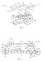
- FIG. 1is an exploded perspective view of an image sensor package in accordance with the present invention.
- FIG. 2is a cross-sectional view of the package taken along the line II—II of FIG. 1 .
- FIG. 3is an upper perspective view of windows in cavities of a lower mold half of a mold in accordance with the present invention.
- FIG. 4is a cross-sectional view along the line IV—IV of FIG. 3 .
- FIG. 5is a cross-sectional view of the mold of FIGS. 3, 4 at a later stage of fabrication.
- FIG. 6is a cross-sectional view of the mold of FIG. 5 at a later stage of fabrication.
- FIG. 7Ais an enlarged cross-sectional view of the region VII of FIG. 6 in accordance with one embodiment of the present invention.
- FIG. 7Bis an enlarged cross-sectional view of the region VII of FIG. 6 in accordance with another embodiment of the present invention.
- FIG. 7Cis an enlarged cross-sectional view of the region VII of FIG. 6 in accordance with yet another embodiment of the present invention.
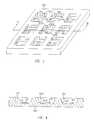
- FIG. 8is a cross-sectional view of an array of image sensor packages during assembly in accordance with the present invention.
- FIG. 9is a cross-sectional view of the array of image sensor packages of FIG. 8 at a later stage of fabrication in accordance with the present invention.
- FIG. 10Ais an enlarged cross-sectional view of the region X of FIG. 6 in accordance with one embodiment of the present invention.
- FIG. 10Bis an enlarged perspective view, partially in cross-section, of the region X of FIG. 6 in accordance with an alternative embodiment of the present invention.
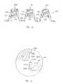
- FIG. 11is a perspective view, partially cutaway and partially exploded, of an image sensor package in accordance with another embodiment of the present invention.
- FIG. 12is a cross-sectional view of the package taken along the line XII—XII of FIG. 11 .
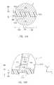
- FIG. 13is a cross-sectional view of a molded window array in accordance with one embodiment of the present invention.
- FIG. 14is an enlarged cross-sectional view of the region XIV of FIG. 13 .
- FIG. 15is an exploded perspective view of an image sensor package in accordance with another embodiment of the present invention.
- FIG. 16is a cross-sectional view of the package taken along the line XVI—XVI of FIG. 15 .
- FIG. 17is a cross-sectional view of the package of FIGS. 15 and 16 illustrating the attachment of a snap lid to a molding.
- FIG. 18Ais an enlarged cross-sectional view of the region XVIII of the package of FIG. 16 in accordance with one embodiment of the present invention.
- FIG. 18Bis an enlarged cross-sectional view of the region XVIII of the package of FIG. 16 in accordance with an alternative embodiment of the present invention.
- a plurality of image sensor packages 100are fabricated simultaneously to minimize the cost associated with each individual package 100 .
- a plurality of windows 122are placed in a mold which includes upper and lower mold halves 300 , 500 (FIG. 5 ). Molding compound is transferred to the mold to form a plurality of moldings 124 (FIG. 6 ), each of moldings 124 enclosing a corresponding window 122 . Moldings 124 are integrally connected together by bridge sections 602 .
- a molded window array 802(FIG. 8 ), which includes windows 122 molded in corresponding moldings 124 , is removed from the mold.
- a substrate 810(FIG. 8) includes a plurality of individual substrates 102 integrally connected together in an array format.
- Image sensors 106are attached to corresponding substrates 102 .
- Bond pads 112 of image sensors 106are electrically connected to corresponding traces 104 of corresponding substrates 102 with corresponding bond wires 114 .
- Molded window array 802is aligned with substrate 810 such that each molding 124 is precisely positioned with respect to a corresponding image sensor 106 . After alignment, molded window array 802 is brought into abutting contact with an upper surface 810 U of substrate 810 such that an adhesive layer 126 attaches molded window array 802 to substrate 810 as shown in FIG. 9 . In one embodiment, moldings 124 are marked and a lower surface 810 L of substrate 810 is populated with interconnection balls 218 . Substrate 810 and attached molded window array 802 are singulated into a plurality of individual packages 100 .
- One advantageis that it is less labor intensive to handle and process a plurality of packages 100 simultaneously rather than to handle and process each package 100 on an individual basis.
- Another advantageis that usage of materials is more efficient when a plurality of packages 100 are fabricated simultaneously. By reducing labor and using less material, the cost associated with each package 100 is minimized.
- molding 124is a low cost molded part.
- molding 124is significantly less expensive than housings of the prior art which were typically ceramic.
- package 100 in accordance with the present inventionis significantly less expensive to manufacture than image sensor assemblies of the prior art.
- a distance ZHsometimes called the Z height, between window 122 and image sensor 106 is precisely controlled to within tight tolerance.
- the windowwas placed on a shelf of a housing after the housing was fabricated. Since a significant tolerance was associated with the window placement, the distance between the window and the image sensor had significant variations from assembly to assembly. However, to insure optimum operation of the image sensor, it is important that the distance between the window and the image sensor be precise. Since the tolerance in this distance is reduced in package 100 , the performance of package 100 is superior to that of the prior art.
- molding 124 of package 100includes a plurality of alignment notches 130 .
- Alignment notches 130are used to align a lens (not shown) to image sensor 106 .
- alignment notches 130facilitates alignment of the lens to image sensor 106 .
- molding 124is precisely aligned to image sensor 106 .
- thisallows the lens to be precisely aligned to image sensor 106 in a single operation by aligning the lens to alignment notches 130 .
- alignment of the lens to image sensor 106is relatively simple. This is in contrast to the prior art, which required a first alignment of the image sensor to the larger substrate and a second alignment of the optics to the larger substrate.
- Enviro-hermetically sealing image sensor 106 in accordance with the present inventionalso reduces complexity and cost in the event image sensor 106 must be repaired or replaced compared to the prior art.
- the housing which hermetically sealed the image sensorwas mounted directly to the larger substrate.
- removal of the housingnecessarily exposed the image sensor to the ambient environment and to dust. For this reason, the image sensor had to be repaired or replaced in a cleanroom or else there was a risk of damaging or destroying the image sensor.
- image sensor 106is enviro-hermetically sealed as part of package 100 .
- Package 100is mounted to the larger substrate, for example, by reflowing interconnection balls 218 .
- package 100is simply removed and a new package 100 is mounted to the larger substrate.
- image sensor 106exposed to the ambient environment during this procedure.
- this procedurecan be performed in any facility with or without a cleanroom.
- the old package 100is discarded or shipped to a central facility for repair. Since package 100 is simple to manufacture and service, the costs associated with package 100 are minimized compared to the prior art.
- molding 124has an interior locking feature 225 I and an exterior locking feature 225 E.
- Molding 124is integral, i.e., is one piece and not a plurality of separate pieces connected together.
- Window 122has an interior surface 122 I and an exterior surface 122 E.
- Exterior locking feature 225 E of molding 124contacts a periphery of exterior surface 122 E of window 122 and interior locking feature 225 I of molding 124 contacts a periphery of interior surface 122 I of window 122 .
- an image sensor package 1100(FIGS. 11, 12 ) includes window 122 and a molding 124 C, where molding 124 C includes a lens holder extension portion 1102 extending upwards, e.g., in a first direction, from window 122 .
- Lens holder extension portion 1102includes a female threaded aperture 1106 extending upwards from window 122 such that window 122 is exposed through aperture 1106 .
- a lens 1210is supported in a lens support 1112 .
- Lens support 1112has a threaded exterior surface 1120 .
- Lens support 1112is threaded into aperture 1106 of lens holder extension portion 1102 .
- lens 1210is readily adjusted relative to image sensor 106 by rotating lens support 1112 . More particularly, lens support 1112 is rotated around a longitudinal axis 1218 of lens support 1112 in a first direction, e.g., clockwise looking down at lens support 1112 , to move lens support 1112 and lens 1210 towards image sensor 106 . Conversely, lens support 1112 is rotated around longitudinal axis 1218 in a second direction opposite the first direction, e.g., counterclockwise looking down at lens support 1112 , to move lens support 1112 and lens 1210 away from image sensor 106 . In this manner, lens support 1112 is rotated until radiation passing through lens 1210 is properly focused on an active area 110 of image sensor 106 . Once proper focus is attained, lens support 1112 is prevented from unintentional rotation. For example, adhesive is applied to secure lens support 1112 to molding 124 C.
- the lens assemblywas typically attached directly to the larger substrate, such as a printed circuit mother board, after the image sensor assembly was attached to the larger substrate.
- a large tolerancewas associated with attachment of the lens assembly in this manner. However, it is important to reduce tolerance to optimize performance of the image sensor assembly.
- the lens assembly of the prior arttypically had to be adjusted by moving the lens assembly relative to the larger substrate, for example with adjustment screws.
- the lens assembly of the prior artwas sometimes inadvertently moved relative to the image sensor which caused defocusing and defective operation of the image sensor.
- the lens assemblywas sometimes bumped during assembly or servicing of the electronic device which used the image sensor assembly.
- the lens assemblymoved due to warpage of the larger substrate.
- package 1100 in accordance with the present inventioneliminates these problems of the prior art.
- molding 124 C including lens holder extension portion 1102is precisely positioned with respect to image sensor 106
- the position of lens 1210 with respect to image sensor 106is also precise to within tight tolerance. Reducing tolerance in the position of lens 1210 with respect to image sensor 106 improves performance of package 1100 compared to prior art image sensor assemblies.
- lens 1210is adjusted relative to image sensor 106 simply by rotating lens support 1112 thus readily allowing focusing of radiation on active area 110 of image sensor 106 .
- this focusingis performed during fabrication of package 1100 before assembly to the larger substrate.
- the prior art requirement of focusing the lens assembly during assembly of the larger substrateis eliminated.
- the costs associated with package 1100are lower than those associated with prior art image sensor assemblies.
- lens support 1112 and lens 1210are integrated into package 1100 , there is essentially no possibility of inadvertently moving lens 1210 relative to image sensor 106 . Thus, the prior art possibility of bumping the lens assembly or otherwise having the lens assembly move and defocus the radiation is eliminated.
- an image sensor package 1500(FIGS. 15, 16 ) includes a molding 124 D having a locking feature 1508 .
- Package 1500further includes a snap lid 1502 having a tab 1612 , where tab 1612 is attached to locking feature 1508 of molding 124 D.
- a window 122 Cis placed in a pocket 1800 (FIG. 18A) of molding 124 D.
- a shelf 1804 of molding 124 Dcontacts and supports a peripheral region 122 IPR of an interior surface 122 I of window 122 C.
- Snap lid 1502is secured in place. Once secured, snap lid 1502 presses against a peripheral region 122 EPR of an exterior surface 122 E of window 122 C.
- window 122 Cis sandwiched between molding 124 D and snap lid 1502 . In this manner, window 122 C is held in place.
- use of snap lid 1502allows window 122 C to be kept in a protective wrapper until window 122 C is needed. For example, window 122 C is kept in a protective wrapper to avoid contamination or scratching of window 122 C.
- window 122 Cis easily removed. Once removed, window 122 C is easily cleaned, treated or replaced with a different window.
- FIG. 1is an exploded perspective view of an image sensor package 100 in accordance with the present invention.
- FIG. 2is a cross-sectional view of package 100 taken along the line II—II of FIG. 1 .
- package 100includes a substrate 102 such as an alumina-based ceramic substrate, a printed circuit board substrate, a plastic glass laminated substrate, or a tape-based substrate.
- Attached to an upper, e.g., first, surface 102 U of substrate 102is an image sensor 106 .
- image sensor 106is a CMOS image sensor device, a charge coupled device (CCD), or a pyroelectric ceramic on CMOS device although other image sensors are used in other embodiments.
- CCDcharge coupled device
- a lower, e.g. first, surface 106 L of image sensor 106is attached by an adhesive layer 108 to upper surface 102 U of substrate 102 although other attachment techniques and/or materials, such as solder, are used in other embodiments.
- a metallization 109 on upper surface 102 Udefines a die attach area of substrate 102 to which image sensor 106 is attached.
- Image sensor 106includes an active area 110 on an upper, e.g., second, surface 106 U of image sensor 106 .
- active area 110is responsive to radiation, e.g., electromagnetic radiation, as is well known to those of skill in the art.
- radiatione.g., electromagnetic radiation
- active area 110is responsive to infrared radiation, ultraviolet light, and/or visible light.
- Image sensor 106further includes a plurality of bond pads 112 on upper surface 106 U of image sensor 106 . Bond pads 112 are connected to internal circuitry of image sensor 106 .
- Substrate 102includes a plurality of electrically conductive traces 104 formed on upper surface 102 U of substrate 102 . Bond pads 112 are electrically connected to corresponding traces 104 by bond wires 114 .
- traces 104are electrically connected to corresponding electrically conductive vias 215 which extend from upper surface 102 U to a lower, e.g., second, surface 102 L of substrate 102 .
- Vias 215are electrically connected to corresponding electrically conductive traces 216 on lower surface 102 L of substrate 102 .
- Formed on traces 216are corresponding electrically conductive pads 217 .
- Formed on pads 217are corresponding electrically conductive interconnection balls 218 such as solder balls. Interconnection balls 218 are used to electrically connect package 100 to a larger substrate (not shown) such as a printed circuit mother board.
- a first bond pad 112 A of the plurality of bond pads 112is electrically connected to a first trace 104 A of the plurality of traces 104 by a first bond wire 114 A of a plurality of bond wires 114 .
- Trace 104 Ais electrically connected to a first via 215 A of the plurality of vias 215 .
- Via 215 Ais electrically connected to a first trace 216 A of the plurality of traces 216 .
- a first conductive pad 217 A of the plurality of conductive pads 217is formed on trace 216 A. Formed on pad 217 A is a first interconnection ball 218 A of the plurality of interconnection balls 218 .
- an electrically conductive pathway between bond pad 112 A and interconnection ball 218 Ais formed by bond wire 114 A, trace 104 A, via 215 A, trace 216 A and pad 217 A.
- the other bond pads 112 , bond wires 114 , traces 104 , vias 215 , traces 216 , pads 217 and interconnection balls 218are electrically connected to one another in a similar fashion so are not discussed further to avoid detracting from the principals of the invention.
- substrate 102is a multi-layered laminated substrate and, instead of straight-through vias 215 , a plurality of electrically conductive traces on various layers in substrate 102 are interconnected by a plurality of electrically conductive vias to form the electrical interconnections between traces 104 and 216 .
- vias 215extend along sides 102 S of substrate 102 and traces 104 and 106 extend to sides 102 S.
- interconnection balls 218are distributed in an array format to form a ball grid array type package.
- interconnection balls 218are not formed, e.g., to form a metal land array type package or a leadless chip carrier (LCC) package.
- LCCleadless chip carrier
- bond pads 112 , traces 104 and bond wires 114are illustrated in FIG. 1, i.e., twenty of each, it is understood that more or less bond pads 112 , traces 104 , bond wires 114 , vias 215 , traces 216 , pads 217 and interconnection balls 218 are typically used depending upon the particular input/output requirements of image sensor 106 .
- Package 100further includes an optical lid 120 , which includes a window 122 and a molding 124 .
- window 122is transparent to the radiation of interest, e.g. to the radiation to which active area 110 of image sensor 106 is responsive.
- window 122is optical glass, germanium or silicon but can be formed of other materials depending upon the application.
- window 122includes one or more filters such as an infrared filter, although in other embodiments window 122 does not include a filter.
- Window 122is typically planar and has no optical power, although in one embodiment, window 122 has optical power, e.g., is a lens.
- Window 122is located above active area 110 of image sensor 106 . It is understood that the term “above” and similar terms are used generally and are not necessarily related to a gravitational reference, e.g., package 100 can be inverted without affecting the operation of package 100 .
- Molding 124is formed of a molding material having excellent adhesion to window 122 .
- molding 124extends inwards beyond sides 122 S of window 122 .
- an exterior locking feature 225 E of molding 124extends over and contacts a periphery of an exterior surface 122 E of window 122
- an interior locking feature 225 I of molding 124extends over and contacts a periphery of an interior surface 122 I of window 122 .
- the periphery of exterior surface 122 E, interior surface 122 Iis the portion of exterior surface 122 E, interior surface 122 I, respectively, directly adjacent sides 122 S of window 122 .
- Sides 122 Sextend between exterior surface 122 E and interior surface 122 I.
- molding 124mechanically locks window 122 in place both top and bottom.
- molding 124extends over the peripheries of exterior and interior surfaces 122 E, 122 I
- molding 124extends over and contacts a periphery of only exterior surface 122 E or, alternatively, only interior surface 122 I.
- molding 124contacts sides 122 S only and does not extend over either interior surface 1221 or exterior surface 122 E.
- Optical lid 120and more particularly, a base 226 of molding 124 is attached to a periphery of upper surface 102 U of substrate 102 by adhesive layer 126 .
- image sensor 106is located and enviro-hermetically sealed in an enclosure formed by substrate 102 , optical lid 120 and adhesive layer 126 .
- the term “enviro-hermetically sealed”means sealed sufficiently to prevent environmental degradation, e.g., from dust or moisture, of package 100 and, more particularly, of image sensor 106 .
- image sensor 106is protected from the ambient environment, e.g., dust and moisture.
- molding 124is formed of a material which is highly resistant to moisture.
- molding 124extend over the peripheries of exterior and interior surfaces 122 E, 122 I of window 122 , the distance which moisture must travel along the interface between molding 124 and window 122 to reach image sensor 106 is maximized thus further preventing moisture ingress into package 100 .
- molding 124is a low cost molded part formed of molding compound.
- molding 124is significantly less expensive than housings of the prior art which were typically ceramic. Accordingly, package 100 is significantly less expensive to manufacture than image sensor assemblies of the prior art.
- a distance ZHis precisely controlled.
- distance ZHis 0.040 inches (1.016 mm) and the tolerance associated with distance ZH is 0.001 inches (0.025 mm).
- the windowwas placed on a shelf of a housing after the housing was fabricated. Since a significant tolerance was associated with the window placement, the distance between the window and the image sensor had significant variations from assembly to assembly. However, to insure optimum operation of the image sensor, it is important that the distance between the window and the image sensor be precise. Since the tolerance in this distance is reduced in package 100 compared to the prior art, the performance of package 100 is superior to that of the prior art.
- molding 124includes a plurality of alignment notches 130 which are used to align an optical axis of a lens (not shown) to the optical center of active area 110 of image sensor 106 .
- This alignmentis generally referred to as aligning a lens to image sensor 106 .
- three alignment notches 130are illustrated, more or less than three alignment notches 130 are used in alternative embodiments.
- alignment notches 130facilitates alignment of the optical axis of the lens to the optical center of active area 110 .
- molding 124is aligned to image sensor 106 and, more particularly, to the optical center of active area 110 , to within tight positional tolerances.
- thisallows the optical axis of the lens to be aligned to within tight positional tolerances, e.g., 0.001 inches (0.025 mm), to the optical center of active area 110 in a single operation by aligning the optical axis of the lens to alignment notches 130 .
- alignment of the optical axis of the lens to the optical center of active area 110is relatively simple compare to the prior art, which required a first alignment of the image sensor to the larger substrate and a second alignment of the optics to the larger substrate.
- Enviro-hermetically sealing image sensor 106also reduces complexity and cost in the event image sensor 106 must be repaired or replaced. Recall that in the prior art, the housing which hermetically sealed the image sensor was mounted directly to the larger substrate. Thus, removal of the housing necessarily exposed the image sensor to the ambient environment and to dust. As a result, the image sensor had to repaired or replaced in a cleanroom or else there was a risk of damaging or destroying the image sensor.
- image sensor 106is enviro-hermetically sealed as part of package 100 .
- Package 100is mounted to the larger substrate, for example, by reflowing interconnection balls 218 as is well known to those of skill in the art.
- To repair or replace image sensor 106package 100 is simply removed and a new package 100 is mounted to the larger substrate. At no time is image sensor 106 exposed to the ambient environment during this procedure.
- this procedurecan be performed in any facility with or without a cleanroom.
- the old package 100is discarded or shipped to a central facility for repair. Since package 100 is simple to manufacture and service, the costs associated with package 100 are minimized compared to the prior art.
- package 100is fabricated simultaneously with a plurality of packages 100 to minimize the cost associated with each individual package 100 .
- FIG. 3is an upper perspective view of a plurality of windows 122 in a plurality of cavities 302 of a lower, e.g., first, mold half 300 of a mold and
- FIG. 4is a cross-sectional view along the line IV—IV of FIG. 3 .
- lower mold half 300defines a three by three (3 ⁇ 3) array of cavities 302 for a total of nine cavities 302 , all of which are similar.
- a mold having a three by three array of cavities 302is set forth, in light of this disclosure, it is understood that a mold having more or less than a three by three array of cavities 302 is used to form more or less, respectively, than nine packages simultaneously.
- first window 122 A of a plurality of windows 122Positioned in a first cavity 302 A of the plurality of cavities 302 is a first window 122 A of a plurality of windows 122 . Each of the other windows 122 is similarly placed in a corresponding cavity 302 so that each of the nine cavities 302 contains one of windows 122 .
- the placement of an article into a mold cavityis well known to those of skill in the art.
- a plurality of tabs 304 Aprotrude from lower mold half 300 into first cavity 302 A.
- three tabs 304 Aexist, but only one tab 304 A is visible in the views of FIGS. 3 and 4.
- a set of tabs 304protrude into each of the other cavities 302 in a similar manner.
- Tabs 304 which include tabs 304 Aresult in the formation of alignment notches 130 (see FIGS. 1, 2 ) as discussed further below.
- FIG. 5is a cross-sectional view of the mold of FIGS. 3, 4 at a later stage of fabrication. After windows 122 are positioned in cavities 302 in lower mold half 300 , an upper, e.g., second, mold half 500 (FIG. 5) is brought down on lower mold half 300 and into the closed position.
- an upper, e.g., second, mold half 500FIG. 5
- upper mold half 500includes a plurality of extensions 502 , all of which are similar, including a first extension 502 A.
- Extension 502 Ais substantially the inverse shape of cavity 302 A and extends downwards from the main body 501 of upper mold half 500 .
- extension 502 Aextends into cavity 302 A and presses against window 122 A.
- a base 504 A of extension 502 Apresses against interior surface 122 I of window 122 A and a base 306 A which defines cavity 302 A of lower mold half 300 presses against exterior surface 122 E of window 122 A.
- the other extensions 502similarly press against the other windows 122 .
- upper mold half 500 and lower mold half 300define a space 506 between upper mold half 500 and lower mold half 300 which is filled with molding compound as shown in FIG. 6 .
- FIG. 6is a cross-sectional view of the mold of FIG. 5 at a later stage of fabrication.
- molding compoundis transferred into space 506 (FIG. 5) to form moldings 124 .
- the transfer of molding compound into a moldis well known to those of skill in the art.
- a molding compoundis heated to a melt and then forced between upper mold half 500 and lower mold half 300 .
- the molding compoundis allowed to cool and solidify.
- the molding compoundshould be mechanically stable over all temperatures to which package 100 may be heated.
- the molding compoundshould be mechanically stable at the temperature which package 100 is heated during attachment to the larger substrate such as the printed circuit mother board.
- the molding compoundis mechanically stable when heated to 220° C. for one minute.
- Suitable molding compoundsare available from Amoco Performance Products, Inc. located in Atlanta, Ga., e.g., A-100, A-200, A-300, R-5000, R-5100, R-5700 resins.
- a first molding 124 A of the plurality of moldings 124encloses window 122 A and surrounds extension 502 A.
- the other moldings 124similarly enclose corresponding windows 122 and surround corresponding extensions 502 .
- windows 122are precisely positioned in moldings 124 to within tight tolerance, e.g., to within 0.001 in. (0.025 mm). As discussed above in reference to FIG. 2, this allows the Z height ZH to be precisely controlled which ensures optimum performance of package 100 . This is in contrast to the prior art where placement of the window on the shelf of the housing after the housing was fabricated resulted in significant variations in the position of the window from assembly to assembly.
- the plurality of moldings 124are integrally connected together. More particularly, bridge sections 602 of molding compound integrally connect adjacent moldings 124 . To illustrate, a first bridge section 602 A of the plurality of bridge sections 602 integrally connects first molding 124 A to an adjacent second molding 124 B of the plurality of moldings 124 .
- FIG. 7Ais an enlarged cross-sectional view of the region VII of FIG. 6 in accordance with one embodiment of the present invention.
- base 504 Apresses directly on interior surface 122 I of window 122 A and base 306 A presses directly on exterior surface 122 E of window 122 A.
- molding compoundis prevented from contacting either interior surface 122 I or exterior surface 122 E of window 122 A.
- molding 124 Acontacts only sides 122 S of window 122 A and does not extend over interior surface 122 I or exterior surface 122 E of window 122 A.
- FIG. 7Bis an enlarged cross-sectional view of the region VII of FIG. 6 in accordance with another embodiment of the present invention. This embodiment is substantially similar with the embodiment illustrated in FIG. 7A with the exception that molding 124 A includes exterior locking feature 225 E and interior locking feature 225 I.
- exterior locking feature 225 Eextends over and contacts a periphery of exterior surface 122 E of window 122 A.
- interior locking feature 225 Iextends over and contacts a periphery of interior surface 122 I of window 122 A.
- Exterior and interior locking features 225 E, 225 Iare flash, i.e., molding compound which is forced between base 306 A and exterior surface 122 E and between base 504 A and interior surface 122 I, respectively, during the transfer of the molding compound to the mold.
- flashi.e., molding compound which is forced between base 306 A and exterior surface 122 E and between base 504 A and interior surface 122 I, respectively, during the transfer of the molding compound to the mold.
- control of flashmay be difficult depending upon the particular application.
- FIG. 7Cis an enlarged cross-sectional view of the region VII of FIG. 6 in accordance with yet another embodiment of the present invention.
- base 504 Aincludes a pad 710 and base 306 A includes a pad 712 .
- Pads 710 , 712are typically a compliant material such a silicone. In one embodiment, pads 710 , 712 are each 0.25 millimeters (mm) thick.
- pad 710contacts a central region 122 ICR of interior surface 122 I of window 122 .
- Central region 122 ICRis surrounded by peripheral region 122 IPR of interior surface 122 I of window 122 A.
- interior surface 122 Iis 8.5 mm square and peripheral region 122 IPR extends inward 1.0 mm from sides 122 S of window 122 A, i.e., central region 122 ICR is located 1.0 mm from sides 122 S of window 122 .
- pad 712contacts a central region 122 ECR of exterior surface 122 E of window 122 A.
- Central region 122 ECRis surrounded by peripheral region 122 EPR of exterior surface 122 E of window 122 A.
- exterior surface 122 Eis 8.5 mm square and peripheral region 122 EPR extends inward 1.0 mm from sides 122 S of window 122 A, i.e., central region 122 ECR is located 1.0 mm from sides 122 S of window 122 .
- pads 710 , 712creates spaces between peripheral regions 122 IPR, 122 EPR and bases 504 A, 306 A, respectively.
- molding compoundfills these spaces during the transfer of the molding compound into the mold.
- interior locking feature 225 Iis formed between peripheral region 122 IPR and base 504 A and exterior locking feature 225 E is formed between peripheral region 122 EPR and base 306 A.
- molding 124 Aincluding interior and exterior locking features 225 I, 225 E, is formed during a single molding step, molding 124 A including interior and exterior locking features 225 I, 225 E is integral, i.e., molding 124 A, interior locking feature 225 I and exterior locking feature 225 E are all the same piece and are not a plurality of separate pieces connected together.
- FIGS. 7B, 7 Cboth interior and exterior locking features 225 I, 225 E are illustrated. However, in an alternative embodiment, only interior locking feature 225 I or exterior locking feature 225 E is formed. As an example, referring to FIG. 7C, only pad 710 or pad 712 is used resulting in the formation of only interior locking feature 225 I or exterior locking feature 225 E, respectively.
- first window 122 A of the plurality of windows 122 in first molding 124 A of the plurality of moldings 124is discussed, in light of this disclosure, it is understood that the other windows 122 are molded in corresponding moldings 124 simultaneously and in a similar manner.
- FIG. 8is a cross-sectional view of an array 800 of image sensor packages 100 during assembly in accordance with the present invention.
- a molded window array 802is removed from the mold, i.e., is removed from lower mold half 300 and upper mold half 500 (see FIG. 6 ).
- Molded window array 802includes windows 122 , which, in this embodiment, are supported by and molded in corresponding moldings 124 .
- first window 122 A of the plurality of windows 122is supported by and molded in first molding 124 A of the plurality of moldings 124 .
- Each of the other windows 122is similarly supported by and molded in a corresponding molding 124 .
- Each of moldings 124include a plurality of alignment notches 130 .
- molding 124 Aincludes three alignment notches 130 A of the plurality of alignment notches 130 although only one alignment notch 130 A is shown in the view of FIG. 8 .
- Alignment notches 130are formed by, and correspond to, tabs 304 of lower mold half 300 (see FIGS. 3 and 4 ).
- array 800includes a substrate 810 .
- Substrate 810includes a plurality of individual substrates 102 integrally connected together in an array format. Each of substrates 102 is delineated and separated by a singulation street 812 which is located between adjacent substrates 102 .
- a first singulation street 812 A of a plurality of singulation streets 812separates a first substrate 102 A of the plurality of substrates 102 from a second substrate 102 B of the plurality of substrates 102 .
- the other substrates 102are similarly separated from adjacent substrates 102 by corresponding singulation streets 812 .
- Substrates 102include traces 104 and metallizations 109 on upper surfaces 102 U of substrates 102 . Substrates 102 also includes vias 215 extending through substrates 102 and traces 216 , pads 217 on lower surfaces 102 L of substrate 102 which are not illustrated in FIG. 8 for purposes of clarity. See vias 215 , traces 216 and pads 217 of FIG. 2 for example. In one embodiment, metalized vias along singulation streets 812 are combined with conductive lands to provide LCC footprints.
- Image sensors 106are attached to corresponding substrates 102 , and more particularly, to corresponding metallizations 109 , by corresponding adhesive layers 108 .
- a first image sensor 106 A of the plurality of image sensors 106is attached to substrate 102 A, and more particularly, to metallization 109 A, by adhesive layer 108 A.
- the other image sensors 106are similarly attached.
- image sensors 106are aligned to substrate 810 using any one of a number of conventional alignment techniques, e.g., are optically or mechanically aligned.
- a pick and place machinesuch as a MRSI 505 by MRSI Corp. of Chelmsford, Mass. is used to align image sensors 106 to substrate 810 .
- MRSI 505by MRSI Corp. of Chelmsford, Mass.
- thisallows image sensors 106 to be precisely aligned to substrate 810 to within tight positional tolerances, e.g., to within 0.001 inches (0.025 mm).
- Bond pads 112 of image sensors 106are electrically connected to corresponding traces 104 by corresponding bond wires 114 .
- a bond pad 112 B of the plurality of bond pads 112is electrically connected to a corresponding trace 104 B of the plurality of traces 104 by a bond wire 114 B of the plurality of bond wires 114 .
- the other bond pads 112are similarly connected.
- Adhesive layer 126is applied to bases 226 of each of moldings 124 and to bridge sections 602 .
- Adhesive layer 126is applied using any one of a number of conventional techniques, e.g., a B stage epoxy is applied by screen printing or needle dispensing or, alternatively, a double sided laminate adhesive tape is applied by pressure.
- adhesive layer 126is applied to selective portions of an upper surface 810 U of substrate 810 , and more particularly, is applied over and extends slightly beyond singulation streets 812 and is applied over a periphery 814 of substrate 810 .
- molded window array 802is aligned with substrate 810 using any one of a number of conventional alignment techniques, e.g., is optically or mechanically aligned. Of importance, molded window array 802 is precisely aligned with substrate 810 , and hence image sensors 106 , to within tight positional tolerance, e.g., to within 0.001 inches (0.025 mm).
- molded window array 802is moved and brought into abutting contact with substrate 810 such that adhesive layer 126 contacts both molded window array 802 and substrate 810 . If necessary, e.g., if adhesive layer 126 is a B staged epoxy, adhesive layer 126 is cured. In this manner, molded window array 802 is attached to substrate 810 by adhesive layer 126 .
- FIG. 9is a cross-sectional view of array 800 of image sensor packages 100 of FIG. 8 at a later stage of fabrication in accordance with the present invention.
- each molding 124 or substrate 102is marked, for example with ink, to identify the part number associated with image sensor package 100 .
- a lower surface 810 L of substrate 810is populated with interconnection balls 218 , e.g., on traces (not shown).
- Array 800is then singulated into a plurality of individual image sensor packages 100 (see FIGS. 1, 2 ) by separating array 800 along singulation streets 812 .
- Singulationcan be accomplished using any one of a number of conventional singulation techniques, e.g. by laser cutting or mechanical sawing through substrate 810 , adhesive layer 126 and bridge sections 602 .
- periphery 814 and the overlying adhesive layer 126 and overlying section of molded window array 802are also trimmed during singulation.
- substrate 810is a snap straight substrate, i.e., is a substrate designed to snap along singulation streets 812 on bending of substrate 810 .
- Snap straight substratestypically ceramic, are well known to those of skill in the art and are not discussed further to avoid detracting from the principles of the invention.
- bridge sections 602 of molded window array 802 and adhesive layer 126are also designed to snap along with substrate 810 along singulation streets 812 .
- Bridge sections 602are formed of a molding compound which is sufficiently brittle to snap. In other embodiments, bridge sections 602 are fabricated to have less strength than the remainder of molded window array 802 to facilitate snapping of bridge sections 602 as discussed in greater detail below with respect to FIGS. 10A, 10 B.
- FIG. 10Ais an enlarged cross-sectional view of the region X of FIG. 6 in accordance with this embodiment of the present invention.
- upper mold half 500includes a tab 1002 which extends from upper mold half 500 downwards towards lower mold half 300 .
- lower mold half 300includes a tab 1004 which extends from lower mold half 300 upwards towards upper mold half 500 .
- Tabs 1002 and 1004are located directly across from one another and define a narrow portion 1006 of bridge section 602 A.
- Narrow portion 1006has a width WNP less than a width WWP of a second wide portion 1008 of bridge section 602 A. Since narrow portion 1006 has less width than wide portion 1008 , narrow portion 1006 has less mechanical strength than wide portion 1008 .
- bridge section 602 Apreferentially snaps apart at narrow portion 1006 when substrate 810 is snapped along a singulation street 812 .
- FIG. 10Bis an enlarged perspective view, partially in cross-section, of the region X of FIG. 6 in accordance with an alternative embodiment of the present invention.
- upper and lower mold halves 500 , 300are not illustrated for purposes of clarity.
- bridge section 602 Aincludes a finger portion 1010 , which is sometimes called webbing.
- Finger portion 1010includes a plurality of fingers 1012 extending between body portions 1014 and 1016 of bridge section 602 A.
- a space 1018exists between each of fingers 1012 along the depth of bridge section 602 A (i.e. along the Z axis of FIG. 10B) and between body portions 1014 , 1016 in the horizontal direction (i.e., along the X axis of FIG. 10 B).
- a first space 1018 A of the plurality of spaces 1018exists between first and second fingers 1012 A, 1012 B of the plurality of fingers 1012 and between body portions 1014 , 1016 .
- each of fingers 1012has a width WFP (along the Y axis of FIG. 10B) less than a width WBP of body portions 1014 , 1016 .
- WFPwidth WBP
- finger portion 1010has less mechanical strength than body portions 1014 , 1016 .
- bridge section 602 Apreferentially snaps apart at finger portion 1010 when substrate 810 is snapped along a singulation street 812 .
- bridge section 602 A of the plurality of bridge sections 602is described and illustrated in each of the embodiments of FIGS. 10A, 10 B, the other bridge sections 602 are similar in structure and function so are not described further.
- One advantageis that it is less labor intensive to handle and process a plurality of packages 100 simultaneously rather than to handle and process each package 100 on an individual basis.
- Another advantageis that usage of materials is more efficient when an array of packages 100 is fabricated. By reducing labor and using less material, the cost associated with each package 100 is minimized.
- packages 100can also be manufactured on an individual basis if desired.
- FIG. 11is a perspective view, partially cutaway and partially exploded, of an image sensor package 1100 in accordance with another embodiment of the present invention.
- FIG. 12is a cross-sectional view of package 1100 taken along the line XII—XII of FIG. 11 .
- package 1100is similar in many respects with package 100 of FIGS. 1 and 2 and the discussion above in reference to package 100 is incorporated herein. To avoid detracting from the principals of the invention, only the relevant differences between packages 1100 and 100 are discussed below.
- Molding 124 C of package 1100includes a lens holder extension portion 1102 .
- Molding 124 C including lens holder extension portion 1102is integral, i.e., is one piece and not a plurality of separate pieces connected together.
- Lens holder extension portion 1102extends upwards, e.g. in a first direction perpendicular to exterior surface 122 E of window 122 , from window 122 .
- Lens holder extension portion 1102includes an interior cylindrical surface 1104 which defines an aperture 1106 .
- a longitudinal axis 1208 of aperture 110 . 6is perpendicular to a plane parallel to window 122 and, more particularly, is perpendicular to exterior and interior surfaces 122 E, 122 I of window 122 in this embodiment.
- Aperture 1106extends upward from window 122 such that window 122 is exposed through aperture 1106 .
- interior cylindrical surfaced 1104is threaded.
- aperture 1106is a female threaded aperture.
- Lens 1210is supported in a support 1112 , hereinafter lens support 1112 .
- Lens support 1112is a cylindrical annulus having an interior cylindrical surface 1214 which defines an aperture 1216 .
- Lens 1210is positioned in aperture 1216 such that lens 1210 and lens support 1112 have a common longitudinal axis 1218 .
- Lens support 1112has an exterior cylindrical surface 1120 , which is threaded. Stated another way, lens support 1112 is male threaded. Of importance, the threading of exterior cylindrical surface 1120 corresponds with the threading of interior cylindrical surface 1104 allowing threaded attachment of lens support 1112 to molding 124 C.
- lens support 1112is positioned above molding 124 C such that longitudinal axes 1208 , 1218 are substantially aligned as best shown in FIG. 12 .
- Lens support 1112is threaded into aperture 1106 so that exterior cylindrical surface 1120 is threadedly attached to interior cylindrical surface 1104 of molding 124 C.
- lens 1210is readily adjusted relative to image sensor 106 by rotating lens support 1112 . More particularly, lens support 1112 is rotated around longitudinal axis 1218 in a first direction, e.g., clockwise looking down at lens support 1112 , to move lens support 1112 and lens 1210 towards image sensor 106 . Conversely, lens support 1112 is rotated around longitudinal axis 1218 in a second direction opposite the first direction, e.g., counterclockwise looking down at lens support 1112 , to move lens support 1112 and lens 1210 away from image sensor 106 . In this manner, lens support 1112 is rotated until radiation passing through lens 1210 is properly focused on active area 110 of image sensor 106 . Once proper focus is attained, lens support 1112 is prevented from unintentional rotation. For example, adhesive is applied to secure lens support 1112 to molding 124 C.
- the lens assemblywas typically attached directly to the larger substrate, such as a printed circuit mother board, after the image sensor assembly was attached to the larger substrate.
- a large tolerancewas associated with attachment of the lens assembly in this manner. However, it is important to reduce tolerances to optimize performance of the image sensor assembly.
- the lens assembly of the prior arttypically had to be adjusted by moving the lens assembly relative to the larger substrate, for example with adjustment screws.
- the lens assembly of the prior artwas sometimes inadvertently moved relative to the image sensor which caused defocusing and defective operation of the image sensor.
- the lens assemblywas sometimes bumped during assembly or servicing of the electronic device which used the image sensor assembly.
- the lens assemblymoved due to warpage of the substrate.
- package 1100 in accordance with the present inventioneliminates these problems of the prior art.
- molding 124 Cis precisely positioned to within tight tolerance of image sensor 106
- the position both horizontally and vertically in the view of FIG. 12 of lens 1210 with respect to image sensor 106is also precise to within tight tolerance, e.g., to within 0.001 in. (0.025 mm).
- the optical axis of lens 1210is precisely aligned with the optical center of active area 110 of image sensor 106 . Reducing tolerance in the position of lens 1210 with respect to image sensor 106 improves performance of package 1100 compared to prior art image sensor assemblies.
- lens 1210is adjusted relative to image sensor 106 simply by rotating lens support 1112 thus readily allowing focusing of radiation on active area 110 of image sensor 106 .
- this focusingis performed during fabrication of package 1100 before assembly to the larger substrate.
- the prior art requirement of focusing the lens assembly during assembly of the larger substrateis eliminated.
- the costs associated with package 1100are lower than those associated with prior art image sensor assemblies.
- lens support 1112 and lens 1210are integrated into package 1100 , there is essentially no possibility of inadvertently moving lens 1210 relative to image sensor 106 . Thus, the prior art possibility of bumping the lens assembly or otherwise having the lens assembly move and defocus the radiation is eliminated.
- Fabrication of package 1100is similar in many respects with fabrication of package 100 of FIGS. 1 and 2 and the discussion above regarding the fabrication of package 100 is incorporated herein. To avoid detracting from the principals of the invention, only the relevant differences between the fabrication of package 1100 and the fabrication of package 100 are discussed below.
- FIG. 13is a cross-sectional view of a molded window array 1300 in accordance with one embodiment of the present invention.
- Molded window array 1300is formed using a multi-piece mold, e.g., a three or four piece mold.
- apertures 1106are formed by molding around threaded plugs, which are then unscrewed from molded window array 1300 .
- Molded window array 1300 of FIG. 13is substantially similar to molded window array 802 of FIG. 8 except that each molding 124 C of molded window array 1300 includes a lens holder extension portion 1102 and a pocket 1302 for supporting a window 122 .
- a first molding 124 C 1 of the plurality of moldings 124 Cincludes a first lens holder extension portion 1102 A of the plurality of lens holder extension portions 1102 and a first pocket 1302 A of the plurality of pockets 1302 .
- the other moldings 124 Chave similar corresponding lens holder extension portions 1102 and pockets 1302 so are not discussed further.
- FIG. 14is an enlarged cross-sectional view of the region XIV of FIG. 13 in accordance with this embodiment of the present invention.
- pocket 1302 Ais shaped to fit and support a window 122 B 1 (window 122 B 1 is not illustrated in FIG. 13 for purposes of clarity). More particularly, pocket 1302 A is essentially the same size and shape as window 122 B 1 .
- Pocket 1302 Ais defined by sides 1404 of molding 124 C 1 which correspond to sides 122 S of window 122 B 1 .
- Pocket 1302 Ais further defined by a shelf 1406 of molding 124 C 1 , which is perpendicular to sides 1404 and extends inwards from sides 1404 . Shelf 1406 corresponds to a peripheral region 122 EPR of an exterior surface 122 E of window 122 B 1 .
- window 122 B 1is secured in pocket 1302 A.
- window 122 B 1is placed into pocket 1302 A and an adhesive is applied to secure window 122 B 1 in place.
- thisallows window 122 B 1 to be kept in a protective wrapper until just before the assembly of molded window array 1300 to the substrate, for example, to substrate 810 of FIG. 8 .
- first window 122 B 1 of a plurality of windows 122to first pocket 1302 A of the plurality of pockets 1302 is discussed above, in light of this disclosure, it is understood that the other windows 122 are secured in corresponding pockets 1302 in a similar manner.
- windows 122are molded into molded window array 1300 during the fabrication of molded window array 1300 . Molding of windows 122 in accordance with this embodiment is substantially similar to molding of windows 122 as discussed in reference to the embodiments of FIGS. 7A, 7 B and 7 C, the discussion of which is incorporated herein.
- FIG. 15is an exploded perspective view of an image sensor package 1500 in accordance with another embodiment of the present invention.
- FIG. 16is a cross-sectional view of package 1500 taken along the line XVI—XVI of FIG. 15 .
- package 1500is similar in many respects with package 100 of FIGS. 1 and 2 and the discussion above in reference to package 100 is incorporated herein. To avoid detracting from the principals of the invention, only the relevant differences between packages 1500 and 100 are discussed below.
- Package 1500includes a snap lid 1502 which snaps onto a molding 124 D of package 1500 to hold a window 122 C in place.
- snap lid 1502is a low cost molded part.
- Snap lid 1502includes a plurality of alignment notches 130 used to align the lens (not shown) to image sensor 106 .
- Snap lid 1502includes a compression ring section 1504 which presses against window 122 C to hold window 122 C in place as discussed further below. Snap lid 1502 further includes a snap 1506 extending downwards from compression ring section 1504 . Snap 1506 snaps onto a corresponding locking feature 1508 of molding 124 D to attach snap lid 1502 to molding 124 D.
- compression ring section 1504is rectangular and includes a rectangular central aperture 1510 .
- a central region of window 122 C(see central region 122 CR of FIGS. 18A and 18B for example) is exposed to the ambient environment through aperture 1510 .
- radiationpasses through aperture 1510 , though window 122 C and strikes active area 110 of image sensor 106 .
- Snap 1506extends downwards from edges of compression ring section 1504 towards molding 124 D, perpendicular to a plane defined by compression ring section 1504 . As shown in FIG. 16, snap 1506 includes an inwardly extending tab 1612 , e.g., a hook-like feature, which is attached to locking feature 1508 of molding 124 D.
- locking feature 1508 of molding 124 Dis shaped as a rectangular bar extending outward in a plane parallel to compression ring section 1504 from molding 124 D along all four sides of molding 124 D.
- Locking feature 1508includes a lip 1614 .
- Tab 1612is in abutting contact with lip 1614 such that snap 1506 encompasses and holds locking feature 1508 thus securing snap lid 1502 to molding 124 D.
- FIG. 17is a cross-sectional view of package 1500 illustrating the attachment of snap lid 1502 to molding 124 D in accordance with this embodiment of the present invention.
- snap lid 1502is aligned with molding 124 D. Once aligned, snap lid 1502 is at a position 1700 .
- snap 1506is laterally aligned to extend around locking feature 1508 . Further, at position 1700 , snap lid 1502 is in its relaxed state, i.e., is not stressed.
- snap lid 1502is snapped onto molding 124 D. To facilitate this snapping, snap lid 1502 is pressed towards molding 124 D. This causes snap 1506 to slide against locking feature 1508 . To facilitate this sliding, snap 1506 includes a taper 1702 which slides against locking feature 1508 .
- snap 1506is distorted and bent away from compression ring section 1504 . This produces stress in snap lid 1502 which causes tab 1612 to press inward against locking feature 1508 .
- snap 1506is distorted and bent and tab 1612 is pressing inward against locking feature 1508 .
- Snap lid 1502is pressed towards molding 124 D until tab 1612 reaches lip 1614 of locking feature 1508 .
- stress in snap lid 1502causes snap 1506 to snap inwards such that tab 1612 engages lip 1614 as shown in FIG. 16 .
- stress created in snap lid 1502 during attachmentfirmly presses snap 1506 around locking feature 1508 so that snap lid 1502 is securely attached to molding 124 D.
- snap lid 1502holds window 122 in place as discussed in reference to FIGS. 18A and 18B.
- FIG. 18Ais an enlarged cross-sectional view of the region XVIII of FIG. 16 in accordance with this embodiment of the present invention.
- window 122 Cis supported in a pocket 1800 defined by sides 1802 and a shelf 1804 of molding 124 D.
- Sides 1802 of molding 124 Dare substantially the same width (in the vertical direction of the view of FIG. 18A) as sides 122 S of window 122 C.
- Shelf 1804is perpendicular to sides 1802 and extends inward from sides 1802 .
- window 122 Cis placed in pocket 1800 .
- shelf 1804contacts and supports a peripheral region 122 IPR of interior surface 122 I of window 122 C.
- Snap lid 1502is secured in place as described in reference to FIG. 17 . Once secured, snap lid 1502 , and more particularly compression ring section 1504 , contacts and presses against a peripheral region 122 EPR of exterior surface 122 E of window 122 C.
- window 122 Cis sandwiched between molding 124 D and snap lid 1502 . In this manner, window 122 C is held in place.
- use of snap lid 1502allows window 122 C to be kept in a protective wrapper until window 122 C is needed. For example, window 122 C is kept in a protective wrapper to avoid contamination or scratching of window 122 C.
- window 122 Callows window 122 C to be easily removed.
- snap 1506FIG. 16
- window 122 C in FIG. 18Aincludes a first layer 1810 such as planar glass and a second layer 1812 such as an infrared filter.
- window 122 Cis a single layer such a single piece of planar glass.
- window 122 Cmay be desirable to prevent window 122 C from being removable.
- window 122 Cis permanently secured to molding 124 D.
- adhesiveis applied to adhere window 122 C in pocket 1800 before snap lid 1502 is secured.
- molding 124 Dis fabricated simultaneously with a plurality of moldings 124 D as part of a molded window array similar to molded window array 802 of FIG. 8 .
- Windows 122 C and snap lids 1502are attached to moldings 124 D while moldings 124 D are still part of the molded window array.
- This attachmentoccurs while the molded window array is separate from a substrate, e.g., substrate 810 of FIG. 8 .
- this attachmentoccurs after the molded window array is attached to a substrate, e.g., substrate 810 of FIG. 9 .
- molding 124 Dis singulated from the other moldings 124 D of the molded window array, window 122 and snap lid 1502 attached, and molding 124 D attached to the individual substrate, e.g. substrate 102 of FIG. 15 .
- FIG. 18Bis an enlarged cross-sectional view of the region XVIII of package 1500 of FIG. 16 in accordance with an alternative embodiment of the present invention.
- the embodiment of FIG. 18Bis substantially similar to the embodiment of FIG. 18A with the exception that sides 1802 A of molding 124 D 1 are shorter than sides 122 S of window 122 C and compression ring section 1504 A of snap lid 1502 A includes a pocket 1820 .
- Pocket 1820 of snap lid 1502 Ais symmetric with pocket 1800 A of molding 124 D 1 .
- Pocket 1820is defined by sides 1822 A and a shelf 1824 of snap lid 1502 A.
- Shelf 1824is perpendicular to sides 1822 A and extends inward from sides 1822 A.
- Sides 1802 A and 1822 Alie on a common plane and the combined width (in the vertical direction in the view of FIG. 18B) of sides 1802 A and 1822 A is substantially equal to the width of sides 122 S of window 122 C.
- Shelfs 1824 , 1804press on peripheral regions 122 EPR, 122 IPR of exterior and interior surfaces 122 E, 122 I, respectively, of window 122 . In this manner, window 122 C is supported in pockets 1800 A and 1820 and held in place.
Landscapes
- Physics & Mathematics (AREA)
- Engineering & Computer Science (AREA)
- Multimedia (AREA)
- Signal Processing (AREA)
- General Physics & Mathematics (AREA)
- Optics & Photonics (AREA)
- Microelectronics & Electronic Packaging (AREA)
- Computer Hardware Design (AREA)
- Power Engineering (AREA)
- Solid State Image Pick-Up Elements (AREA)
- Lens Barrels (AREA)
Abstract
Description
Claims (20)
Priority Applications (10)
| Application Number | Priority Date | Filing Date | Title |
|---|---|---|---|
| US10/286,589US6791076B2 (en) | 1999-12-08 | 2002-10-31 | Image sensor package |
| US10/928,475US6956201B2 (en) | 1999-12-08 | 2004-08-26 | Image sensor package fabrication method |
| US11/119,234US7126111B2 (en) | 1999-12-08 | 2005-04-28 | Camera module having a threaded lens barrel and a ball grid array connecting device |
| US11/526,168US7199359B2 (en) | 1999-12-08 | 2006-09-21 | Camera module fabrication method including singulating a substrate |
| US11/706,726US7332712B2 (en) | 1999-12-08 | 2007-02-14 | Camera module fabrication method including the step of removing a lens mount and window from the mold |
| US12/005,081US20080106624A1 (en) | 1999-12-08 | 2007-12-21 | Method of using a camera module |
| US12/930,884US20110115918A1 (en) | 1999-12-08 | 2011-01-18 | Camera module having lens mount with ir filter |
| US13/350,619US8994860B2 (en) | 1999-12-08 | 2012-01-13 | Molded image sensor package and method |
| US13/837,283US9332164B2 (en) | 1999-12-08 | 2013-03-15 | Molded semiconductor package with snap lid |
| US15/143,682US9735191B2 (en) | 1999-12-08 | 2016-05-02 | Molded semiconductor package |
Applications Claiming Priority (2)
| Application Number | Priority Date | Filing Date | Title |
|---|---|---|---|
| US09/457,513US6483101B1 (en) | 1999-12-08 | 1999-12-08 | Molded image sensor package having lens holder |
| US10/286,589US6791076B2 (en) | 1999-12-08 | 2002-10-31 | Image sensor package |
Related Parent Applications (1)
| Application Number | Title | Priority Date | Filing Date |
|---|---|---|---|
| US09/457,513ContinuationUS6483101B1 (en) | 1999-12-08 | 1999-12-08 | Molded image sensor package having lens holder |
Related Child Applications (1)
| Application Number | Title | Priority Date | Filing Date |
|---|---|---|---|
| US10/928,475ContinuationUS6956201B2 (en) | 1999-12-08 | 2004-08-26 | Image sensor package fabrication method |
Publications (2)
| Publication Number | Publication Date |
|---|---|
| US20030057359A1 US20030057359A1 (en) | 2003-03-27 |
| US6791076B2true US6791076B2 (en) | 2004-09-14 |
Family
ID=23817029
Family Applications (11)
| Application Number | Title | Priority Date | Filing Date |
|---|---|---|---|
| US09/457,513Expired - LifetimeUS6483101B1 (en) | 1999-12-08 | 1999-12-08 | Molded image sensor package having lens holder |
| US10/286,589Expired - LifetimeUS6791076B2 (en) | 1999-12-08 | 2002-10-31 | Image sensor package |
| US10/928,475Expired - LifetimeUS6956201B2 (en) | 1999-12-08 | 2004-08-26 | Image sensor package fabrication method |
| US11/119,234Expired - LifetimeUS7126111B2 (en) | 1999-12-08 | 2005-04-28 | Camera module having a threaded lens barrel and a ball grid array connecting device |
| US11/526,168Expired - LifetimeUS7199359B2 (en) | 1999-12-08 | 2006-09-21 | Camera module fabrication method including singulating a substrate |
| US11/706,726Expired - LifetimeUS7332712B2 (en) | 1999-12-08 | 2007-02-14 | Camera module fabrication method including the step of removing a lens mount and window from the mold |
| US12/005,081AbandonedUS20080106624A1 (en) | 1999-12-08 | 2007-12-21 | Method of using a camera module |
| US12/930,884AbandonedUS20110115918A1 (en) | 1999-12-08 | 2011-01-18 | Camera module having lens mount with ir filter |
| US13/350,619Expired - Fee RelatedUS8994860B2 (en) | 1999-12-08 | 2012-01-13 | Molded image sensor package and method |
| US13/837,283Expired - Fee RelatedUS9332164B2 (en) | 1999-12-08 | 2013-03-15 | Molded semiconductor package with snap lid |
| US15/143,682Expired - Fee RelatedUS9735191B2 (en) | 1999-12-08 | 2016-05-02 | Molded semiconductor package |
Family Applications Before (1)
| Application Number | Title | Priority Date | Filing Date |
|---|---|---|---|
| US09/457,513Expired - LifetimeUS6483101B1 (en) | 1999-12-08 | 1999-12-08 | Molded image sensor package having lens holder |
Family Applications After (9)
| Application Number | Title | Priority Date | Filing Date |
|---|---|---|---|
| US10/928,475Expired - LifetimeUS6956201B2 (en) | 1999-12-08 | 2004-08-26 | Image sensor package fabrication method |
| US11/119,234Expired - LifetimeUS7126111B2 (en) | 1999-12-08 | 2005-04-28 | Camera module having a threaded lens barrel and a ball grid array connecting device |
| US11/526,168Expired - LifetimeUS7199359B2 (en) | 1999-12-08 | 2006-09-21 | Camera module fabrication method including singulating a substrate |
| US11/706,726Expired - LifetimeUS7332712B2 (en) | 1999-12-08 | 2007-02-14 | Camera module fabrication method including the step of removing a lens mount and window from the mold |
| US12/005,081AbandonedUS20080106624A1 (en) | 1999-12-08 | 2007-12-21 | Method of using a camera module |
| US12/930,884AbandonedUS20110115918A1 (en) | 1999-12-08 | 2011-01-18 | Camera module having lens mount with ir filter |
| US13/350,619Expired - Fee RelatedUS8994860B2 (en) | 1999-12-08 | 2012-01-13 | Molded image sensor package and method |
| US13/837,283Expired - Fee RelatedUS9332164B2 (en) | 1999-12-08 | 2013-03-15 | Molded semiconductor package with snap lid |
| US15/143,682Expired - Fee RelatedUS9735191B2 (en) | 1999-12-08 | 2016-05-02 | Molded semiconductor package |
Country Status (4)
| Country | Link |
|---|---|
| US (11) | US6483101B1 (en) |
| AU (1) | AU4134301A (en) |
| TW (1) | TW472369B (en) |
| WO (1) | WO2001043202A2 (en) |
Cited By (67)
| Publication number | Priority date | Publication date | Assignee | Title |
|---|---|---|---|---|
| US20040212078A1 (en)* | 2003-04-28 | 2004-10-28 | Smattech, Inc. | Package structure and sensor module using the same |
| US20040266051A1 (en)* | 2003-06-30 | 2004-12-30 | Sanyo Electric Co., Ltd. | Method for manufacturing a solid-state image sensing device, such as a CCD |
| US20050041123A1 (en)* | 2003-08-20 | 2005-02-24 | Sbc Knowledge Ventures, L.P. | Digital image capturing system and method |
| US20050046973A1 (en)* | 2003-07-17 | 2005-03-03 | Stmicroelectronics Sa | Method for fixing a lens of an optic group with respect to an optical sensor inside an electronic device able to acquire images and corresponding device |
| US20050103987A1 (en)* | 2003-10-06 | 2005-05-19 | Stmicroelectronics S.A. | Semiconductor component, wafer and package having an optical sensor |
| US20050110889A1 (en)* | 2003-11-26 | 2005-05-26 | Tuttle Mark E. | Packaged microelectronic imagers and methods of packaging microelectronic imagers |
| US6934065B2 (en)* | 2003-09-18 | 2005-08-23 | Micron Technology, Inc. | Microelectronic devices and methods for packaging microelectronic devices |
| US20050184219A1 (en)* | 2004-02-23 | 2005-08-25 | Kirby Kyle K. | Packaged microelectronic imagers and methods of packaging microelectronic imagers |
| US20050237637A1 (en)* | 2004-04-23 | 2005-10-27 | Premier Image Technology Corporation | Lens module and assembling method thereof |
| US20050254133A1 (en)* | 2004-05-13 | 2005-11-17 | Salman Akram | Integrated optics units and methods of manufacturing integrated optics units for use with microelectronic imagers |
| US20050253213A1 (en)* | 2004-05-13 | 2005-11-17 | Tongbi Jiang | Covers for microelectronic imagers and methods for wafer-level packaging of microelectronics imagers |
| US20050275049A1 (en)* | 2004-06-10 | 2005-12-15 | Kirby Kyle K | Packaged microelectronic imagers and methods of packging microelectronic imagers |
| US20050275048A1 (en)* | 2004-06-14 | 2005-12-15 | Farnworth Warren M | Microelectronic imagers and methods of packaging microelectronic imagers |
| US20050275750A1 (en)* | 2004-06-09 | 2005-12-15 | Salman Akram | Wafer-level packaged microelectronic imagers and processes for wafer-level packaging |
| US20050275051A1 (en)* | 2004-06-14 | 2005-12-15 | Farnworth Warren M | Prefabricated housings for microelectronic imagers and methods for packaging microelectronic imagers |
| US20050285154A1 (en)* | 2004-06-29 | 2005-12-29 | Salman Akram | Packaged microelectronic imagers and methods of packaging microelectronic imagers |
| US20050287783A1 (en)* | 2004-06-29 | 2005-12-29 | Kirby Kyle K | Microelectronic devices and methods for forming interconnects in microelectronic devices |
| US20060011809A1 (en)* | 2004-07-19 | 2006-01-19 | Farnworth Warren M | Microelectronic imagers with optical devices and methods of manufacturing such microelectronic imagers |
| US20060014313A1 (en)* | 2004-07-16 | 2006-01-19 | Hall Frank L | Microelectronic imaging units and methods of manufacturing microelectronic imaging units |
| US20060024856A1 (en)* | 2004-07-28 | 2006-02-02 | Derderian James M | Microelectronic imaging units and methods of manufacturing microelectronic imaging units |
| US20060027740A1 (en)* | 1999-12-08 | 2006-02-09 | Amkor Technology, Inc. | Snap lid camera module |
| US20060040421A1 (en)* | 2004-08-19 | 2006-02-23 | Farnworth Warren M | Spacers for packaged microelectronic imagers and methods of making and using spacers for wafer-level packaging of imagers |
| US20060038183A1 (en)* | 2004-08-19 | 2006-02-23 | Oliver Steven D | Microelectronic imagers with curved image sensors and methods for manufacturing microelectronic imagers |
| US20060043599A1 (en)* | 2004-09-02 | 2006-03-02 | Salman Akram | Through-wafer interconnects for photoimager and memory wafers |
| US20060043262A1 (en)* | 2004-08-30 | 2006-03-02 | Micron Technology, Inc. | Microelectronic imagers with integrated optical devices and methods for manufacturing such microelectronic imagers |
| US20060046332A1 (en)* | 2004-08-26 | 2006-03-02 | Derderian James M | Microelectronic Imaging units and methods of manufacturing microelectronic imaging units |
| US20060043509A1 (en)* | 2004-08-24 | 2006-03-02 | Watkins Charles M | Packaged microelectronic imaging devices and methods of packaging microelectronic imaging devices |
| US20060044433A1 (en)* | 2004-08-31 | 2006-03-02 | Micron Technology, Inc. | Microelectronic imagers having front side contacts and methods of packaging such microelectronic imagers |
| US20060043512A1 (en)* | 2004-08-24 | 2006-03-02 | Oliver Steven D | Microelectronic imagers with optical devices having integral reference features and methods for manufacturing such microelectronic imagers |
| US7056811B2 (en) | 2003-06-10 | 2006-06-06 | Sanyo Electric Co., Ltd. | Method for manufacturing semiconductor device |
| US20060148250A1 (en)* | 2004-12-30 | 2006-07-06 | Micron Technology, Inc. | Methods for forming interconnects in microelectronic workpieces and microelectronic workpieces formed using such methods |
| US20060175532A1 (en)* | 2005-02-08 | 2006-08-10 | Micron Technology, Inc. | Microelectronic imaging units and methods of manufacturing microelectronic imaging units |
| US20060177959A1 (en)* | 2005-02-10 | 2006-08-10 | Micron Technology, Inc. | Microfeature workpieces having microlenses and methods of forming microlenses on microfeature workpieces |
| US20060186492A1 (en)* | 2005-02-18 | 2006-08-24 | Micron Technology, Inc. | Microelectronic imagers with shaped image sensors and methods for manufacturing microelectronic imagers |
| US20060216850A1 (en)* | 2004-08-10 | 2006-09-28 | Street Bret K | Microelectronic imaging units and methods of manufacturing microelectronic imaging units |
| US20060221225A1 (en)* | 2005-03-29 | 2006-10-05 | Sharp Kabushiki Kaisha | Optical device module, optical path fixing device, and method for manufacturing optical device module |
| US20060219884A1 (en)* | 2005-03-29 | 2006-10-05 | Sharp Kabushiki Kaisha | Optical device module, and method of fabricating the optical device module |
| US20060289968A1 (en)* | 2005-06-28 | 2006-12-28 | Micron Technology, Inc. | Conductive interconnect structures and formation methods using supercritical fluids |
| US20070025715A1 (en)* | 2005-07-29 | 2007-02-01 | Hon Hai Precision Industry Co., Ltd. | Camera module with a position detecting mechanism |
| US20070045858A1 (en)* | 2005-09-01 | 2007-03-01 | Micron Technology, Inc. | Microfeature workpieces and methods for forming interconnects in microfeature workpieces |
| US20070045515A1 (en)* | 2005-09-01 | 2007-03-01 | Micron Technology, Inc. | Microelectronic imaging devices and associated methods for attaching transmissive elements |
| US20070047879A1 (en)* | 2005-08-29 | 2007-03-01 | Samsung Electro-Mechanics Co., Ltd. | Optical modulator module package |
| US20070064317A1 (en)* | 2005-09-22 | 2007-03-22 | Po-Hung Chen | Image sensor package structure |
| US20070125632A1 (en)* | 2005-12-07 | 2007-06-07 | Taiwan Ic Packaging Corporation | Contact sensor and method for making the same |
| US20070148807A1 (en)* | 2005-08-22 | 2007-06-28 | Salman Akram | Microelectronic imagers with integrated optical devices and methods for manufacturing such microelectronic imagers |
| US20070166867A1 (en)* | 2006-01-04 | 2007-07-19 | Chow Seng G | Integrated circuit package system with image sensor system |
| US20070177266A1 (en)* | 2006-02-01 | 2007-08-02 | Seiko Epson Corporation | Optical module and method for manufacturing the same |
| US20080106624A1 (en)* | 1999-12-08 | 2008-05-08 | Amkor Technology, Inc. | Method of using a camera module |
| US20080174684A1 (en)* | 2007-01-23 | 2008-07-24 | Nec Electronics Corporation | Solid-state imaging device |
| US7425499B2 (en) | 2004-08-24 | 2008-09-16 | Micron Technology, Inc. | Methods for forming interconnects in vias and microelectronic workpieces including such interconnects |
| US20080251705A1 (en)* | 2007-04-10 | 2008-10-16 | Hon Hai Precision Industry Co., Ltd. | Image sensor chip package |
| US20090046184A1 (en)* | 2007-08-14 | 2009-02-19 | Hon Hai Precision Industry Co., Ltd. | Image sensor |
| US20090102004A1 (en)* | 2007-10-18 | 2009-04-23 | Hon Hai Precision Industry Co., Ltd. | Sensor package |
| US20090109327A1 (en)* | 2007-10-24 | 2009-04-30 | Hon Hai Precision Industry Co., Ltd. | Camera module |
| US7622377B2 (en) | 2005-09-01 | 2009-11-24 | Micron Technology, Inc. | Microfeature workpiece substrates having through-substrate vias, and associated methods of formation |
| US7652376B2 (en) | 2006-01-04 | 2010-01-26 | Stats Chippac Ltd. | Integrated circuit package system including stacked die |
| US20100032830A1 (en)* | 2008-08-06 | 2010-02-11 | Industrial Technology Research Institute | Three-dimensional conducting structure and method of fabricating the same |
| US7687315B2 (en) | 2005-04-29 | 2010-03-30 | Stats Chippac Ltd. | Stacked integrated circuit package system and method of manufacture therefor |
| US7750482B2 (en) | 2006-02-09 | 2010-07-06 | Stats Chippac Ltd. | Integrated circuit package system including zero fillet resin |
| US7768125B2 (en) | 2006-01-04 | 2010-08-03 | Stats Chippac Ltd. | Multi-chip package system |
| US20100194465A1 (en)* | 2009-02-02 | 2010-08-05 | Ali Salih | Temperature compensated current source and method therefor |
| US7855100B2 (en) | 2005-03-31 | 2010-12-21 | Stats Chippac Ltd. | Integrated circuit package system with an encapsulant cavity and method of fabrication thereof |
| US7936033B2 (en) | 2008-12-29 | 2011-05-03 | Texas Instruments Incorporated | Micro-optical device packaging system |
| US20110204508A1 (en)* | 2010-02-22 | 2011-08-25 | In Sang Yoon | Semiconductor packaging system with an aligned interconnect and method of manufacture thereof |
| TWI387087B (en)* | 2008-08-06 | 2013-02-21 | Ind Tech Res Inst | Three-dimensional conducting structure and method of fabricating the same |
| US8704349B2 (en) | 2006-02-14 | 2014-04-22 | Stats Chippac Ltd. | Integrated circuit package system with exposed interconnects |
| US20140233115A1 (en)* | 2011-09-30 | 2014-08-21 | Konica Minolta Advanced Layers, Inc. | Image Pickup Lens Unit And Method For Manufacturing Image Pickup Lens Unit |
Families Citing this family (180)
| Publication number | Priority date | Publication date | Assignee | Title |
|---|---|---|---|---|
| US20080128844A1 (en)* | 2002-11-18 | 2008-06-05 | Tessera North America | Integrated micro-optical systems and cameras including the same |
| US20010007475A1 (en)* | 2000-01-06 | 2001-07-12 | Asahi Kogaku Kogyo Kabushiki Kaisha | Image pickup device and its mounting structure for an optical low-pass filter |
| CN1225111C (en)* | 2000-03-02 | 2005-10-26 | 奥林巴斯光学工业株式会社 | small camera module |
| JP4405062B2 (en)* | 2000-06-16 | 2010-01-27 | 株式会社ルネサステクノロジ | Solid-state imaging device |
| US6684034B2 (en)* | 2000-12-15 | 2004-01-27 | Chi Wang Tseng | Optical signal receiving device |
| US6624954B2 (en)* | 2001-06-15 | 2003-09-23 | Logitech Europe S.A. | Lens mounting apparatus |
| US6654187B2 (en)* | 2001-07-16 | 2003-11-25 | Alex Ning | Camera lens carrier for circuit board mounting |
| US6717126B1 (en)* | 2001-07-16 | 2004-04-06 | Amkor Technology, Inc. | Method of fabricating and using an image sensor package with reflector |
| US6686580B1 (en) | 2001-07-16 | 2004-02-03 | Amkor Technology, Inc. | Image sensor package with reflector |
| KR100431260B1 (en)* | 2001-08-29 | 2004-05-12 | 삼성전기주식회사 | Image module |
| JP2003163378A (en)* | 2001-11-26 | 2003-06-06 | Citizen Electronics Co Ltd | Surface mount type light emitting diode and method of manufacturing the same |
| JP4033669B2 (en)* | 2001-12-04 | 2008-01-16 | シャープ株式会社 | The camera module |
| JP4096588B2 (en)* | 2002-03-22 | 2008-06-04 | コニカミノルタホールディングス株式会社 | Imaging device |
| US7074638B2 (en) | 2002-04-22 | 2006-07-11 | Fuji Photo Film Co., Ltd. | Solid-state imaging device and method of manufacturing said solid-state imaging device |
| DE10226135B4 (en)* | 2002-06-12 | 2004-08-05 | Siemens Ag | Optical module and optical system |
| US6977187B2 (en) | 2002-06-19 | 2005-12-20 | Foster-Miller, Inc. | Chip package sealing method |
| US20040012708A1 (en)* | 2002-07-18 | 2004-01-22 | Matherson Kevin James | Optical prefilter system that provides variable blur |
| EP1686619A3 (en)* | 2002-07-29 | 2007-01-03 | Fuji Photo Film Co., Ltd. | Solid-state imaging device and method of manufacturing the same |
| US7473218B2 (en)* | 2002-08-06 | 2009-01-06 | Olympus Corporation | Assembling method of capsule medical apparatus |
| US7564496B2 (en)* | 2002-09-17 | 2009-07-21 | Anteryon B.V. | Camera device, method of manufacturing a camera device, wafer scale package |
| US7038288B2 (en)* | 2002-09-25 | 2006-05-02 | Microsemi Corporation | Front side illuminated photodiode with backside bump |
| WO2004047421A2 (en) | 2002-11-14 | 2004-06-03 | Donnelly Corporation | Imaging system for vehicle |
| SG111092A1 (en) | 2002-11-15 | 2005-05-30 | St Microelectronics Pte Ltd | Semiconductor device package and method of manufacture |
| US20040113048A1 (en)* | 2002-12-16 | 2004-06-17 | Tu Hsiu Wen | Image sensor module |
| US20040113047A1 (en)* | 2002-12-16 | 2004-06-17 | Hsiu Wen Tu | Image sensor module |
| FR2849275B1 (en)* | 2002-12-24 | 2005-04-15 | St Microelectronics Sa | METHOD FOR ASSEMBLING AN OPTICAL SYSTEM IN FRONT OF AN OPTICAL HOUSING |
| US7215374B2 (en)* | 2003-01-03 | 2007-05-08 | Micron Technology, Inc. | Camera module having geared lens barrel |
| US20040150740A1 (en)* | 2003-01-30 | 2004-08-05 | Hsin Chung Hsien | Miniaturized image sensor module |
| JP4223851B2 (en)* | 2003-03-31 | 2009-02-12 | ミツミ電機株式会社 | Small camera module |
| FR2854498B1 (en)* | 2003-04-29 | 2005-09-16 | St Microelectronics Sa | OPTICAL SENSOR SEMICONDUCTOR HOUSING INSERTING INSIDE AN OBJECT. |
| JP4510403B2 (en)* | 2003-05-08 | 2010-07-21 | 富士フイルム株式会社 | Camera module and method for manufacturing camera module |
| WO2004107437A1 (en)* | 2003-05-30 | 2004-12-09 | Valen Technologies (S) Pte Ltd | Image sensing module and method for constructing the same |
| TWI237358B (en)* | 2003-06-27 | 2005-08-01 | Hon Hai Prec Ind Co Ltd | Packaging structure of imaging sensor |
| US7330211B2 (en)* | 2003-07-08 | 2008-02-12 | Micron Technology, Inc. | Camera module with focus adjustment structure and systems and methods of making the same |
| US7329861B2 (en)* | 2003-10-14 | 2008-02-12 | Micron Technology, Inc. | Integrally packaged imaging module |
| TWI229777B (en)* | 2003-11-28 | 2005-03-21 | United Microelectronics Corp | Camera module and packaging method |
| US7091571B1 (en) | 2003-12-11 | 2006-08-15 | Amkor Technology, Inc. | Image sensor package and method for manufacture thereof |
| TWI244174B (en)* | 2003-12-31 | 2005-11-21 | Siliconware Precision Industries Co Ltd | Photosensitive semiconductor package and method for fabricating the same |
| US7872686B2 (en)* | 2004-02-20 | 2011-01-18 | Flextronics International Usa, Inc. | Integrated lens and chip assembly for a digital camera |
| JP2005286888A (en)* | 2004-03-30 | 2005-10-13 | Fuji Photo Film Co Ltd | Solid-state imaging apparatus |
| DE102004018222A1 (en)* | 2004-04-15 | 2005-11-10 | Robert Bosch Gmbh | Opto-electronic module |
| US7061106B2 (en)* | 2004-04-28 | 2006-06-13 | Advanced Chip Engineering Technology Inc. | Structure of image sensor module and a method for manufacturing of wafer level package |
| WO2005109861A1 (en)* | 2004-05-04 | 2005-11-17 | Tessera, Inc. | Compact lens turret assembly |
| US20060109366A1 (en)* | 2004-05-04 | 2006-05-25 | Tessera, Inc. | Compact lens turret assembly |
| JP2005347416A (en)* | 2004-06-01 | 2005-12-15 | Sharp Corp | Solid-state imaging device, semiconductor wafer, and camera module |
| JP5252770B2 (en)* | 2004-06-10 | 2013-07-31 | 三星電子株式会社 | Image sensor package assembly method |
| TWM267483U (en)* | 2004-07-16 | 2005-06-11 | Kingpak Tech Inc | Image sensor module |
| DE102004051379A1 (en)* | 2004-08-23 | 2006-03-23 | Osram Opto Semiconductors Gmbh | Device for an optoelectronic component and component with an optoelectronic component and a device |
| US7205532B2 (en)* | 2004-08-24 | 2007-04-17 | Avago Technologies Ecbu Ip (Singapore) Pte. Ltd. | Integrated ball grid array optical mouse sensor packaging |
| TWI333249B (en)* | 2004-08-24 | 2010-11-11 | Himax Tech Inc | Sensor package |
| FR2875055B1 (en)* | 2004-09-06 | 2006-12-01 | Kingpak Tech Inc | IMAGE SENSOR MODULE STRUCTURE |
| GB2417826B (en)* | 2004-09-16 | 2006-08-09 | Kingpak Tech Inc | Image sensor module structure |
| US7196322B1 (en)* | 2004-10-08 | 2007-03-27 | Kingpak Technology Inc. | Image sensor package |
| KR100608420B1 (en)* | 2004-11-01 | 2006-08-02 | 동부일렉트로닉스 주식회사 | Image sensor chip package and manufacturing method thereof |
| KR20060087273A (en)* | 2005-01-28 | 2006-08-02 | 삼성전기주식회사 | Semiconductor package and manufacturing method |
| KR100724885B1 (en)* | 2005-03-23 | 2007-06-04 | 삼성전자주식회사 | Camera lens module |
| US7519291B2 (en)* | 2005-03-24 | 2009-04-14 | Fujifilm Corporation | Digital camera, lens unit, and camera system having the same |
| KR100691157B1 (en)* | 2005-04-07 | 2007-03-09 | 삼성전기주식회사 | Focusing Adjustable Camera Module |
| US7227236B1 (en) | 2005-04-26 | 2007-06-05 | Amkor Technology, Inc. | Image sensor package and its manufacturing method |
| US20070272827A1 (en)* | 2005-04-27 | 2007-11-29 | Amkor Technology, Inc. | Image sensor package having mount holder attached to image sensor die |
| TWI254389B (en)* | 2005-04-29 | 2006-05-01 | Sigurd Microelectronics Corp | Package structure of photo sensor and manufacturing method thereof |
| US7710496B2 (en)* | 2005-06-16 | 2010-05-04 | Basler Ag | Carrier for a circuit board on which a sensor component is held in a defined position |
| US7576401B1 (en) | 2005-07-07 | 2009-08-18 | Amkor Technology, Inc. | Direct glass attached on die optical module |
| JP4864364B2 (en)* | 2005-07-11 | 2012-02-01 | Hoya株式会社 | Imaging unit for electronic endoscope |
| KR100809682B1 (en)* | 2005-07-11 | 2008-03-06 | 삼성전자주식회사 | Method for manufacturing optical device with transparent cover and method for manufacturing optical device module using same |
| JP4585409B2 (en)* | 2005-08-24 | 2010-11-24 | 株式会社東芝 | Small camera module |
| US20070057169A1 (en)* | 2005-09-14 | 2007-03-15 | Chung-Chi Hsiao | Package structure for an optical sensor |
| FR2891088A1 (en)* | 2005-09-20 | 2007-03-23 | St Microelectronics Sa | STRUCTURE FOR MOUNTING A MOBILE OBJECTIVE ABOVE AN OPTICAL SENSOR |
| US20070075235A1 (en)* | 2005-09-30 | 2007-04-05 | Po-Hung Chen | Packaging structure of a light-sensing element with reduced packaging area |
| US7960767B2 (en)* | 2005-10-15 | 2011-06-14 | Aptina Imaging Corporation | System for programmable gate array with sensor array |
| CN101816008A (en)* | 2005-10-28 | 2010-08-25 | 马格纳电子系统公司 | Camera module for vehicle vision system |
| US20070108544A1 (en)* | 2005-11-17 | 2007-05-17 | Tu Hsiu W | Image sensor with a compound structure |
| GB2433665B (en)* | 2005-12-20 | 2009-09-23 | Kingpak Tech Inc | An image sensor module structure |
| KR100744925B1 (en)* | 2005-12-27 | 2007-08-01 | 삼성전기주식회사 | Camera module package |
| US20070145254A1 (en)* | 2005-12-28 | 2007-06-28 | Feng Chen | Packaging method for an assembly of image-sensing chip and circuit board |
| KR100741619B1 (en)* | 2006-01-03 | 2007-07-23 | 킹팍 테크놀로지 인코포레이티드 | Image sensor module structure manufacturing method |
| JP2007184801A (en)* | 2006-01-10 | 2007-07-19 | Alps Electric Co Ltd | The camera module |
| TWI267208B (en)* | 2006-01-18 | 2006-11-21 | Visera Technologies Co Ltd | Image sensor module |
| TWI274441B (en)* | 2006-01-27 | 2007-02-21 | Sunplus Technology Co Ltd | Solderable CCM |
| TWM299861U (en)* | 2006-04-03 | 2006-10-21 | Largan Precision Co Ltd | Screw thread structure of optical lens |
| JP2007288755A (en)* | 2006-04-14 | 2007-11-01 | Optopac Co Ltd | The camera module |
| JP2007300488A (en)* | 2006-05-01 | 2007-11-15 | Alps Electric Co Ltd | Camera module |
| US7498646B2 (en)* | 2006-07-19 | 2009-03-03 | Advanced Chip Engineering Technology Inc. | Structure of image sensor module and a method for manufacturing of wafer level package |
| US8013289B2 (en) | 2006-11-15 | 2011-09-06 | Ether Precision, Inc. | Lens array block for image capturing unit and methods of fabrication |
| CN101191884A (en)* | 2006-11-22 | 2008-06-04 | 鸿富锦精密工业(深圳)有限公司 | Lens module and its debugging method |
| US7566854B2 (en)* | 2006-12-08 | 2009-07-28 | Advanced Chip Engineering Technology Inc. | Image sensor module |
| CN101285921A (en)* | 2007-04-13 | 2008-10-15 | 鸿富锦精密工业(深圳)有限公司 | Imaging module |
| US7671326B2 (en)* | 2007-04-27 | 2010-03-02 | Casio Computer Co., Ltd. | Image inputting apparatus |
| KR100833312B1 (en)* | 2007-05-10 | 2008-05-28 | 삼성전기주식회사 | Camera module |
| CN101320119A (en)* | 2007-06-04 | 2008-12-10 | 鸿富锦精密工业(深圳)有限公司 | Camera module group |
| JP4344760B2 (en)* | 2007-06-15 | 2009-10-14 | シャープ株式会社 | Solid-state imaging device and electronic apparatus including the same |
| JP4344761B2 (en)* | 2007-06-15 | 2009-10-14 | シャープ株式会社 | Solid-state imaging device and electronic apparatus including the same |
| US20090046201A1 (en)* | 2007-08-14 | 2009-02-19 | Shoppertrak Rct Corporation | Holding apparatus for a camera lens |
| JP2009055554A (en)* | 2007-08-29 | 2009-03-12 | Fujifilm Corp | Flexible imaging device equipped with multiple imaging elements |
| CN101442061B (en)* | 2007-11-20 | 2011-11-09 | 鸿富锦精密工业(深圳)有限公司 | Camera component |
| US9350976B2 (en) | 2007-11-26 | 2016-05-24 | First Sensor Mobility Gmbh | Imaging unit of a camera for recording the surroundings with optics uncoupled from a circuit board |
| DE102007057172B4 (en)* | 2007-11-26 | 2009-07-02 | Silicon Micro Sensors Gmbh | Stereo camera for environmental detection |
| US20090235984A1 (en)* | 2008-03-21 | 2009-09-24 | Atomic Energy Council - Institute Of Nuclear Energy Research | Solar cell module |
| KR100956380B1 (en)* | 2008-08-06 | 2010-05-07 | 삼성전기주식회사 | Camera module and manufacturing method thereof |
| KR100950917B1 (en)* | 2008-08-06 | 2010-04-01 | 삼성전기주식회사 | Camera module and manufacturing method thereof |
| US20100038519A1 (en)* | 2008-08-12 | 2010-02-18 | Cho-Yi Lin | Image Sensing Module |
| US7813043B2 (en) | 2008-08-15 | 2010-10-12 | Ether Precision, Inc. | Lens assembly and method of manufacture |
| US8482664B2 (en) | 2008-10-16 | 2013-07-09 | Magna Electronics Inc. | Compact camera and cable system for vehicular applications |
| KR20100058345A (en)* | 2008-11-24 | 2010-06-03 | 삼성전자주식회사 | Methods of forming camera modules |
| WO2010091347A1 (en) | 2009-02-06 | 2010-08-12 | Magna Electronics Inc. | Improvements to camera for vehicle |
| US12328491B1 (en) | 2009-03-25 | 2025-06-10 | Magna Electronics Inc. | Vehicular camera and lens assembly |
| ES2693455T3 (en) | 2009-03-25 | 2018-12-11 | Magna Electronics Inc. | Camera assembly and vehicular lens |
| JP4391585B1 (en)* | 2009-06-08 | 2009-12-24 | 新光電気工業株式会社 | Camera module and manufacturing method thereof |
| US8090250B2 (en)* | 2009-06-23 | 2012-01-03 | Ether Precision, Inc. | Imaging device with focus offset compensation |
| US20110062571A1 (en)* | 2009-09-11 | 2011-03-17 | St-Ericsson Sa | Optical device, integrated circuit device and system |
| TWI406562B (en)* | 2009-10-30 | 2013-08-21 | Ability Entpr Co Ltd | Image detecting module and camera module |
| DE102009056658B4 (en)* | 2009-12-02 | 2018-10-25 | Conti Temic Microelectronic Gmbh | Lens for a semiconductor camera and method for focusing a semiconductor camera |
| US8830389B2 (en) | 2010-02-12 | 2014-09-09 | Ability Enterprise Co., Ltd. | Image detecting module and lens module |
| KR101984632B1 (en)* | 2010-04-01 | 2019-05-31 | 콘티 테믹 마이크로일렉트로닉 게엠베하 | Device comprising an optical module and support plate |
| KR101123159B1 (en)* | 2010-07-06 | 2012-03-20 | 엘지이노텍 주식회사 | Camera module |
| US8299589B2 (en)* | 2010-07-26 | 2012-10-30 | TDK Taiwan, Corp. | Packaging device of image sensor |
| KR101128931B1 (en)* | 2010-08-11 | 2012-03-27 | 삼성전기주식회사 | Camera module |
| WO2012036626A1 (en)* | 2010-09-16 | 2012-03-22 | Medha Dharmatilleke | Methods and camera systems for recording and creation of 3-dimension (3-d) capable videos and 3-dimension (3-d) still photos |
| US8982269B2 (en)* | 2010-09-27 | 2015-03-17 | Omnivision Technologies, Inc. | Mechanical assembly for fine focus of a wafer-level camera module, and associated methods |
| EP2487480B1 (en)* | 2011-02-09 | 2014-01-15 | ABB Technology AG | Optical sensor element and optical sample analysing apparatus |
| US9380219B2 (en) | 2011-04-20 | 2016-06-28 | Magna Electronics Inc. | Angular filter for vehicle mounted cameras |
| KR101853827B1 (en) | 2011-04-29 | 2018-05-02 | 엘지이노텍 주식회사 | Camera module |
| CN102231383B (en)* | 2011-06-17 | 2013-02-20 | 瑞声声学科技(深圳)有限公司 | Ceramic packing device and method of image sensor |
| WO2013015929A1 (en)* | 2011-07-22 | 2013-01-31 | Alex Ning | Lens mount |
| CN103858425B (en) | 2011-08-02 | 2018-03-30 | 马格纳电子系统公司 | Vehicle camera system |
| US9871971B2 (en) | 2011-08-02 | 2018-01-16 | Magma Electronics Inc. | Vehicle vision system with light baffling system |
| JP2013038628A (en)* | 2011-08-09 | 2013-02-21 | Sony Corp | Camera module, manufacturing apparatus, and manufacturing method |
| US8388793B1 (en)* | 2011-08-29 | 2013-03-05 | Visera Technologies Company Limited | Method for fabricating camera module |
| US20130215253A1 (en)* | 2012-02-16 | 2013-08-22 | Pawel Achtel | Underwater lens mount system for underwater motion picture cameras |
| US9661235B2 (en)* | 2012-04-13 | 2017-05-23 | Blackmagic Design Pty Ltd. | Camera having a separate image capture module and a method of assembling the camera |
| US9307128B2 (en) | 2012-06-26 | 2016-04-05 | Alex Ning | Lens mount |
| US9609754B2 (en)* | 2013-01-22 | 2017-03-28 | Kyocera Corporation | Package for mounting electronic element, electronic device, and imaging module |
| CN104349079B (en)* | 2013-07-29 | 2018-07-24 | 光宝科技股份有限公司 | Image sensing module |
| US9204025B1 (en) | 2013-08-30 | 2015-12-01 | Amazon Technologies, Inc. | Camera module with a molded enclosure contained in a flexible substrate |
| US9241097B1 (en) | 2013-09-27 | 2016-01-19 | Amazon Technologies, Inc. | Camera module including image sensor die in molded cavity substrate |
| JP6214337B2 (en)* | 2013-10-25 | 2017-10-18 | キヤノン株式会社 | Electronic parts, electronic devices, and methods for manufacturing electronic parts. |
| US9161449B2 (en)* | 2013-10-29 | 2015-10-13 | Lite-On Technology Corporation | Image sensor module having flat material between circuit board and image sensing chip |
| US9451138B2 (en) | 2013-11-07 | 2016-09-20 | Magna Electronics Inc. | Camera for vehicle vision system |
| JP6444029B2 (en)* | 2013-12-26 | 2018-12-26 | キヤノン株式会社 | Detection device and imaging device including the same |
| US9749509B2 (en) | 2014-03-13 | 2017-08-29 | Magna Electronics Inc. | Camera with lens for vehicle vision system |
| TWI503589B (en)* | 2014-04-23 | 2015-10-11 | Image capturing module for increasing assembly flatness and decreasing focusing time and method of assembling the same | |
| EP2942938B1 (en)* | 2014-05-07 | 2021-01-27 | Veoneer Sweden AB | Camera module for a motor vehicle and method of pre-focusing a lens objective in a lens holder |
| US20160062073A1 (en)* | 2014-08-28 | 2016-03-03 | Himax Technologies Limited | Image sensor module and method for adjusting focus of image sensor module |
| US10729001B2 (en) | 2014-08-31 | 2020-07-28 | Skyworks Solutions, Inc. | Devices and methods related to metallization of ceramic substrates for shielding applications |
| US9276140B1 (en)* | 2014-09-16 | 2016-03-01 | Amazon Technologies, Inc. | Imager module with interposer chip |
| US9634053B2 (en)* | 2014-12-09 | 2017-04-25 | Taiwan Semiconductor Manufacturing Co., Ltd. | Image sensor chip sidewall interconnection |
| US9525002B2 (en) | 2015-01-05 | 2016-12-20 | Stmicroelectronics Pte Ltd | Image sensor device with sensing surface cavity and related methods |
| US9955054B2 (en) | 2015-02-05 | 2018-04-24 | Robert Bosch Gmbh | Camera and method for assembling with fixed final alignment |
| US20160282175A1 (en)* | 2015-03-24 | 2016-09-29 | Semiconductor Components Industries, Llc | Removable protective cap for an image sensor |
| US9728510B2 (en) | 2015-04-10 | 2017-08-08 | Analog Devices, Inc. | Cavity package with composite substrate |
| US9977250B2 (en) | 2015-09-25 | 2018-05-22 | Microsoft Technology Licensing, Llc | Self-registering lenses |
| US10250004B2 (en) | 2015-11-05 | 2019-04-02 | Magna Electronics Inc. | Method of forming a connector for an electrical cable for electrically connecting to a camera of a vehicle |
| US10351072B2 (en) | 2015-11-05 | 2019-07-16 | Magna Electronics Inc. | Vehicle camera with modular construction |
| US10230875B2 (en) | 2016-04-14 | 2019-03-12 | Magna Electronics Inc. | Camera for vehicle vision system |
| US10560613B2 (en) | 2015-11-05 | 2020-02-11 | Magna Electronics Inc. | Vehicle camera with modular construction |
| CN105633108B (en)* | 2015-12-10 | 2024-04-12 | 格科微电子(上海)有限公司 | Multi-camera module and assembly method thereof |
| US10192914B2 (en)* | 2016-03-20 | 2019-01-29 | Ningbo Sunny Opotech Co., Ltd. | Camera module and array camera module with circuit board unit and photosensitive unit and manufacturing method thereof |
| US10142532B2 (en) | 2016-04-08 | 2018-11-27 | Magna Electronics Inc. | Camera for vehicle vision system |
| WO2017181668A1 (en)* | 2016-04-21 | 2017-10-26 | 宁波舜宇光电信息有限公司 | Camera module and array camera module based on integration packaging process |
| US10718922B2 (en)* | 2016-06-01 | 2020-07-21 | Ams Sensors Singapore Pte. Ltd. | Optoelectronic module including lens barrel comprising flanges and adhesive thereon and resting directly on a cover glass |
| US10925160B1 (en) | 2016-06-28 | 2021-02-16 | Amazon Technologies, Inc. | Electronic device with a display assembly and silicon circuit board substrate |
| US10237456B2 (en) | 2016-08-22 | 2019-03-19 | Magna Electronics Inc. | Vehicle camera assembly process |
| TWI600321B (en) | 2016-12-13 | 2017-09-21 | 財團法人工業技術研究院 | Composite array camera lens module |
| US11049898B2 (en) | 2017-04-01 | 2021-06-29 | Ningbo Sunny Opotech Co., Ltd. | Systems and methods for manufacturing semiconductor modules |
| JP7075415B2 (en)* | 2017-04-12 | 2022-05-25 | ▲寧▼波舜宇光▲電▼信息有限公司 | Imaging module and its molded photosensitive assembly, manufacturing method and electronic equipment |
| US20190027531A1 (en)* | 2017-07-19 | 2019-01-24 | Omnivision Technologies, Inc. | Image sensor module having protective structure |
| JP2019041172A (en)* | 2017-08-23 | 2019-03-14 | 住友電気工業株式会社 | Image sensor device and imaging device |
| US10694085B2 (en) | 2017-09-01 | 2020-06-23 | Mtd Products Inc | Optical sensor housing |
| CN109510925A (en)* | 2017-09-15 | 2019-03-22 | 南昌欧菲光电技术有限公司 | Camera module |
| FR3073356A1 (en)* | 2017-11-06 | 2019-05-10 | Stmicroelectronics (Grenoble 2) Sas | ENCAPSULATION COVER FOR ELECTRONIC HOUSING AND METHOD OF MANUFACTURE |
| FR3073980A1 (en)* | 2017-11-23 | 2019-05-24 | Stmicroelectronics (Grenoble 2) Sas | ENCAPSULATION COVER FOR ELECTRONIC HOUSING AND METHOD OF MANUFACTURE |
| EP3502775A1 (en)* | 2017-12-19 | 2019-06-26 | DURA Operating, LLC | A visual recognition system of a vehicle, and a method for implementing such system |
| US20210321025A1 (en) | 2018-08-21 | 2021-10-14 | Ningbo Sunny Opotech Co., Ltd. | Camera module and molded photosensitive assembly and manufacturing methods thereof, and electronic device |
| US11683911B2 (en) | 2018-10-26 | 2023-06-20 | Magna Electronics Inc. | Vehicular sensing device with cooling feature |
| US11438487B2 (en) | 2019-03-07 | 2022-09-06 | Magna Electronics Inc. | Vehicular camera with thermal interface material |
| CN112243074A (en)* | 2019-07-18 | 2021-01-19 | 三赢科技(深圳)有限公司 | Lens module |
| CN112751993B (en)* | 2019-10-29 | 2025-02-11 | 晋城三赢精密电子有限公司 | Base, camera module and electronic device |
| DE102020209779A1 (en) | 2020-08-04 | 2022-02-10 | Robert Bosch Gesellschaft mit beschränkter Haftung | Image capture device and a method for manufacturing an image capture device |
| TWI804052B (en)* | 2021-06-04 | 2023-06-01 | 同欣電子工業股份有限公司 | Non-soldering type sensor lens |
| US12088902B2 (en) | 2022-08-23 | 2024-09-10 | Changxin Memory Technologies, Inc. | Camera module and electronic device |
Citations (48)
| Publication number | Priority date | Publication date | Assignee | Title |
|---|---|---|---|---|
| US3018689A (en) | 1959-05-28 | 1962-01-30 | Bausch & Lomb | Optical system for electro-optical switching apparatus |
| GB1022329A (en) | 1963-07-26 | 1966-03-09 | Texas Instruments Inc | Semiconductor device container |
| US3880529A (en) | 1966-04-25 | 1975-04-29 | Hughes Aircraft Co | Sighting device |
| US4055761A (en) | 1975-03-14 | 1977-10-25 | Nippon Kogaku K.K. | Light receiving device for photoelectric conversion element |
| US4210922A (en) | 1975-11-28 | 1980-07-01 | U.S. Philips Corporation | Charge coupled imaging device having selective wavelength sensitivity |
| US4293190A (en) | 1978-05-31 | 1981-10-06 | Oakeridge Management Services B.V. | Transparency viewers |
| US4390220A (en) | 1981-04-02 | 1983-06-28 | Burroughs Corporation | Electrical connector assembly for an integrated circuit package |
| US4433886A (en) | 1981-12-17 | 1984-02-28 | Elco Corporation | Connector mounting for integrated circuit chip packages |
| US4582350A (en) | 1983-10-13 | 1986-04-15 | Canon Kabushiki Kaisha | Helically threaded mechanism |
| US4744009A (en) | 1986-10-31 | 1988-05-10 | Amp Incorporated | Protective carrier and securing means therefor |
| US4801998A (en) | 1984-08-20 | 1989-01-31 | Oki Electric Industry Co., Ltd. | EPROM device |
| US4843313A (en) | 1984-12-26 | 1989-06-27 | Hughes Aircraft Company | Integrated circuit package carrier and test device |
| US4936784A (en) | 1988-07-18 | 1990-06-26 | Hirose Electric Co., Ltd. | Electronic component socket |
| US4971930A (en) | 1985-12-20 | 1990-11-20 | Sgs Microelectronics S.P.A. | EPROM semiconductor device erasable with ultraviolet rays and manufacturing process thereof |
| US4980635A (en) | 1984-12-26 | 1990-12-25 | Hughes Aircraft Company | Integrated circuit package carrier |
| US4999142A (en) | 1988-06-07 | 1991-03-12 | Matsushita Electric Industrial Co., Ltd. | Method of molding a lens array |
| US5001315A (en) | 1988-07-08 | 1991-03-19 | Square D Company | Circuit breaker auxiliary device snap-on package and method of assembling same |
| US5037187A (en)* | 1988-08-12 | 1991-08-06 | Kyocera Corporation | Zoom lens mount assembly |
| US5191481A (en) | 1990-09-17 | 1993-03-02 | Asahi Kogaku Kogyo Kabushiki Kaisha | Lens installation in an optical device |
| WO1993022787A1 (en) | 1992-04-28 | 1993-11-11 | Lsi Logic Corporation | Arrangement for mounting a lens to a solid state image sensor |
| US5424531A (en) | 1992-12-31 | 1995-06-13 | Apple Computer, Inc. | Method and apparatus for coupling an optical lens to an imaging electronics array |
| US5444520A (en) | 1993-05-17 | 1995-08-22 | Kyocera Corporation | Image devices |
| US5579164A (en) | 1993-11-12 | 1996-11-26 | Pharos Technology Corporation | Spatially multiplexed image display system |
| US5590787A (en) | 1995-01-04 | 1997-01-07 | Micron Technology, Inc. | UV light sensitive die-pac for securing semiconductor dies during transport |
| US5615052A (en) | 1993-04-16 | 1997-03-25 | Bruce W. McCaul | Laser diode/lens assembly |
| US5617131A (en) | 1993-10-28 | 1997-04-01 | Kyocera Corporation | Image device having a spacer with image arrays disposed in holes thereof |
| US5692083A (en) | 1996-03-13 | 1997-11-25 | The Whitaker Corporation | In-line unitary optical device mount and package therefor |
| US5764424A (en) | 1996-10-02 | 1998-06-09 | Mcdonnell Douglas Corporation | Precision extender lens for stereo vision systems |
| US5801374A (en) | 1996-11-04 | 1998-09-01 | Rockwell International | Precision optical sensor packaging |
| US5811799A (en)* | 1997-07-31 | 1998-09-22 | Wu; Liang-Chung | Image sensor package having a wall with a sealed cover |
| US5818634A (en)* | 1996-08-05 | 1998-10-06 | Motorola, Inc. | Dual mode optical Magnifier system |
| US5821532A (en) | 1997-06-16 | 1998-10-13 | Eastman Kodak Company | Imager package substrate |
| US5825033A (en)* | 1996-10-31 | 1998-10-20 | The Arizona Board Of Regents On Behalf Of The University Of Arizona | Signal processing method for gamma-ray semiconductor sensor |
| US5825954A (en)* | 1996-10-18 | 1998-10-20 | American Products, Inc. | Submersible fiber optics lens assembly |
| US5867368A (en) | 1997-09-09 | 1999-02-02 | Amkor Technology, Inc. | Mounting for a semiconductor integrated circuit device |
| US5949655A (en) | 1997-09-09 | 1999-09-07 | Amkor Technology, Inc. | Mounting having an aperture cover with adhesive locking feature for flip chip optical integrated circuit device |
| US6011661A (en) | 1998-04-07 | 2000-01-04 | Weng; Leo | Optical holder for an optical apparatus |
| US6037655A (en) | 1998-01-12 | 2000-03-14 | Eastman Kodak Company | Linear image sensor package assembly |
| US6134057A (en)* | 1997-09-17 | 2000-10-17 | Minolta Co., Ltd. | Drive and guide mechanism and apparatus using the mechanism |
| US6188841B1 (en) | 1998-05-27 | 2001-02-13 | Fuji Photo Film Co., Ltd. | Lens-fitted film unit with plastic taking lens |
| US6236046B1 (en)* | 1997-10-28 | 2001-05-22 | Matsushita Electric Works, Ltd. | Infrared sensor |
| US6243540B1 (en)* | 1998-11-24 | 2001-06-05 | Olympus Optical Co., Ltd. | Lens barrel assembly |
| US6266197B1 (en) | 1999-12-08 | 2001-07-24 | Amkor Technology, Inc. | Molded window array for image sensor packages |
| US6270222B1 (en) | 1995-10-06 | 2001-08-07 | Robert D. Herpst | Protective window assembly and method of using the same for a laser beam generating apparatus |
| US6384472B1 (en) | 2000-03-24 | 2002-05-07 | Siliconware Precision Industries Co., Ltd | Leadless image sensor package structure and method for making the same |
| US6389687B1 (en) | 1999-12-08 | 2002-05-21 | Amkor Technology, Inc. | Method of fabricating image sensor packages in an array |
| US6455774B1 (en) | 1999-12-08 | 2002-09-24 | Amkor Technology, Inc. | Molded image sensor package |
| US6483101B1 (en)* | 1999-12-08 | 2002-11-19 | Amkor Technology, Inc. | Molded image sensor package having lens holder |
Family Cites Families (84)
| Publication number | Priority date | Publication date | Assignee | Title |
|---|---|---|---|---|
| US499142A (en)* | 1893-06-06 | John wesley neff | ||
| US3170588A (en)* | 1963-05-17 | 1965-02-23 | Jr Joe M Lyon | Snap release container |
| US3853237A (en)* | 1972-11-16 | 1974-12-10 | Ethyl Dev Corp | Vial or container with safety closure |
| US3880528A (en)* | 1973-07-02 | 1975-04-29 | Tektronix Inc | Light probe |
| US3971841A (en)* | 1974-06-20 | 1976-07-27 | Polaroid Corporation | Molding devices and process for making a molded plastic lens mount |
| US4491865A (en)* | 1982-09-29 | 1985-01-01 | Welch Allyn, Inc. | Image sensor assembly |
| JPS59228755A (en) | 1983-06-09 | 1984-12-22 | Toshiba Corp | Solid state image sensor |
| GB2146504A (en) | 1983-09-09 | 1985-04-17 | Electronic Automation Ltd | Image recording device |
| JPS6288345A (en)* | 1985-10-15 | 1987-04-22 | Seiko Epson Corp | Plastic encapsulated solid image sensor |
| JPH0422528Y2 (en) | 1985-11-22 | 1992-05-22 | ||
| JPS62224047A (en) | 1986-03-26 | 1987-10-02 | Hitachi Ltd | Solid-state image pickup device |
| JPS63308375A (en)* | 1987-06-10 | 1988-12-15 | Hitachi Ltd | solid-state imaging device |
| JP2569053B2 (en)* | 1987-06-26 | 1997-01-08 | キヤノン株式会社 | Image sensor |
| US5274456A (en)* | 1987-12-28 | 1993-12-28 | Hitachi, Ltd. | Semiconductor device and video camera unit using it and their manufacturing method |
| US5023442A (en)* | 1988-06-21 | 1991-06-11 | Rohm Co., Ltd. | Apparatus for optically writing information |
| EP0355522B1 (en)* | 1988-08-18 | 1993-12-15 | Seiko Epson Corporation | Solid state image pickup device |
| US5122861A (en)* | 1988-11-25 | 1992-06-16 | Fuji Photo Film Co., Ltd. | Solid state image pickup device having particular package structure |
| US5400072A (en)* | 1988-12-23 | 1995-03-21 | Hitachi, Ltd. | Video camera unit having an airtight mounting arrangement for an image sensor chip |
| JP3216650B2 (en)* | 1990-08-27 | 2001-10-09 | オリンパス光学工業株式会社 | Solid-state imaging device |
| US5412229A (en)* | 1990-08-31 | 1995-05-02 | Sumitomo Electric Industries, Ltd. | Semiconductor light detecting device making use of a photodiode chip |
| JPH04111479A (en)* | 1990-08-31 | 1992-04-13 | Sumitomo Electric Ind Ltd | Light-receiving element |
| US5113290A (en)* | 1990-12-13 | 1992-05-12 | Honeywell Inc. | Sealed focusing assembly for an industrial vision system |
| JP3096171B2 (en)* | 1991-09-30 | 2000-10-10 | ローム株式会社 | Image sensor and electronic device incorporating the same |
| JP2954760B2 (en)* | 1991-09-30 | 1999-09-27 | ローム株式会社 | Image sensor |
| DE69324406T2 (en)* | 1992-06-11 | 1999-11-11 | Canon K.K., Tokio/Tokyo | Contact image sensor, method for its production and information processing device |
| TW332348B (en)* | 1992-06-23 | 1998-05-21 | Sony Co Ltd | Manufacturing method for solid state motion picture device provides a highly accurate and low cost solid state motion picture device by use of empty package made of resin. |
| US5302778A (en)* | 1992-08-28 | 1994-04-12 | Eastman Kodak Company | Semiconductor insulation for optical devices |
| JP2843464B2 (en)* | 1992-09-01 | 1999-01-06 | シャープ株式会社 | Solid-state imaging device |
| US5902993A (en)* | 1992-12-28 | 1999-05-11 | Kyocera Corporation | Image scanner for image inputting in computers, facsimiles word processor, and the like |
| DE69421434T2 (en)* | 1993-04-07 | 2000-06-08 | Mitsui Chemicals, Inc. | PCB for optical elements |
| US5355283A (en)* | 1993-04-14 | 1994-10-11 | Amkor Electronics, Inc. | Ball grid array with via interconnection |
| JPH07142761A (en)* | 1993-11-18 | 1995-06-02 | Mitsubishi Electric Corp | Photoreceptor element and its array, device and method for sensing picture |
| JP3202856B2 (en)* | 1993-12-28 | 2001-08-27 | 株式会社リコー | Image reading device |
| DE69527473T2 (en) | 1994-05-09 | 2003-03-20 | Nec Corp., Tokio/Tokyo | Semiconductor arrangement consisting of a semiconductor chip, which is connected by means of contact bumps on the printed circuit board, and assembly method |
| US5655189A (en)* | 1994-05-27 | 1997-08-05 | Kyocera Corporation | Image device having thermally stable light emitting/receiving arrays and opposing lenses |
| KR0146262B1 (en)* | 1994-07-05 | 1998-09-15 | 김광호 | Image overlay image processor |
| US5608262A (en)* | 1995-02-24 | 1997-03-04 | Lucent Technologies Inc. | Packaging multi-chip modules without wire-bond interconnection |
| US6498624B1 (en)* | 1995-02-28 | 2002-12-24 | Canon Kabushiki Kaisha | Optical apparatus and image sensing apparatus mounted on the same surface of a board |
| US6392703B1 (en)* | 1995-02-28 | 2002-05-21 | Canon Kabushiki Kaisha | Optical apparatus for forming an object image on a sensing element |
| US5825560A (en)* | 1995-02-28 | 1998-10-20 | Canon Kabushiki Xaisha | Optical apparatus |
| US5651493A (en)* | 1995-04-24 | 1997-07-29 | International Business Machines Corporation | Method of performing solder joint analysis of semi-conductor components |
| US5604362A (en)* | 1995-04-24 | 1997-02-18 | Xerox Corporation | Filter architecture for a photosensitive chip |
| JP3004578B2 (en)* | 1995-05-12 | 2000-01-31 | 財団法人工業技術研究院 | Integrated Circuit Package Consisting of Multi-Heat Conductors for Enhanced Heat Dissipation and Caps Around the Edge for Improved Package Integrity and Reliability |
| US6060722A (en)* | 1995-05-15 | 2000-05-09 | Havens; William H. | Optical reader having illumination assembly including improved aiming pattern generator |
| KR20040004472A (en)* | 1995-05-31 | 2004-01-13 | 소니 가부시끼 가이샤 | Image pickup apparatus, fabrication method thereof, image pickup adaptor apparatus, signal processing apparatus, signal processing method thereof, information processing apparatus, and information processing method |
| JPH0921938A (en) | 1995-07-05 | 1997-01-21 | Nisshin Koki Kk | Mounting structure for lens frame |
| US5861654A (en)* | 1995-11-28 | 1999-01-19 | Eastman Kodak Company | Image sensor assembly |
| DE69632228T2 (en)* | 1995-07-13 | 2005-04-14 | Eastman Kodak Co. | Image sensor with a carrier housing |
| JPH09181287A (en)* | 1995-10-24 | 1997-07-11 | Sony Corp | Light receiving device and manufacturing method thereof |
| US5804827A (en)* | 1995-10-27 | 1998-09-08 | Nikon Corporation | Infrared ray detection device and solid-state imaging apparatus |
| KR100201380B1 (en)* | 1995-11-15 | 1999-06-15 | 김규현 | Heat Dissipation Structure of BGA Semiconductor Package |
| JPH09232548A (en) | 1996-02-20 | 1997-09-05 | Sony Corp | Solid state image device |
| US6011294A (en)* | 1996-04-08 | 2000-01-04 | Eastman Kodak Company | Low cost CCD packaging |
| US5838703A (en) | 1996-09-30 | 1998-11-17 | Motorola, Inc. | Semiconductor laser package with power monitoring system and optical element |
| US6034429A (en)* | 1997-04-18 | 2000-03-07 | Amkor Technology, Inc. | Integrated circuit package |
| JPH10302587A (en) | 1997-04-30 | 1998-11-13 | Stanley Electric Co Ltd | Optical sensor |
| JPH10321827A (en) | 1997-05-16 | 1998-12-04 | Sony Corp | Imaging device and camera |
| US5834839A (en) | 1997-05-22 | 1998-11-10 | Lsi Logic Corporation | Preserving clearance between encapsulant and PCB for cavity-down single-tier package assembly |
| US5808873A (en)* | 1997-05-30 | 1998-09-15 | Motorola, Inc. | Electronic component assembly having an encapsulation material and method of forming the same |
| US5932875A (en)* | 1997-07-07 | 1999-08-03 | Rockwell Science Center, Inc. | Single piece integrated package and optical lid |
| US6982742B2 (en) | 1997-10-06 | 2006-01-03 | Adair Edwin L | Hand-held computers incorporating reduced area imaging devices |
| JP3988239B2 (en)* | 1998-03-19 | 2007-10-10 | ソニー株式会社 | Solid-state imaging device and manufacturing method thereof |
| US6020582A (en)* | 1998-03-31 | 2000-02-01 | Intel Corporation | Light selective element for imaging applications |
| US6157085A (en) | 1998-04-07 | 2000-12-05 | Citizen Watch Co., Ltd. | Semiconductor device for preventing exfoliation from occurring between a semiconductor chip and a resin substrate |
| US6762796B1 (en)* | 1998-08-10 | 2004-07-13 | Olympus Optical Co., Ltd. | Image pickup module having integrated lens and semiconductor chip |
| US6130448A (en)* | 1998-08-21 | 2000-10-10 | Gentex Corporation | Optical sensor package and method of making same |
| US6042412A (en)* | 1998-08-28 | 2000-03-28 | The Whitaker Corporation | Land grid array connector assembly |
| US6753922B1 (en)* | 1998-10-13 | 2004-06-22 | Intel Corporation | Image sensor mounted by mass reflow |
| US6191359B1 (en)* | 1998-10-13 | 2001-02-20 | Intel Corporation | Mass reflowable windowed package |
| DE19958229B4 (en)* | 1998-12-09 | 2007-05-31 | Fuji Electric Co., Ltd., Kawasaki | Optical semiconductor sensor device |
| US6184514B1 (en)* | 1998-12-18 | 2001-02-06 | Eastman Kodak Company | Plastic cover for image sensors |
| US6303924B1 (en) | 1998-12-21 | 2001-10-16 | Microsoft Corporation | Image sensing operator input device |
| US6147389A (en)* | 1999-06-04 | 2000-11-14 | Silicon Film Technologies, Inc. | Image sensor package with image plane reference |
| US6490166B1 (en) | 1999-06-11 | 2002-12-03 | Intel Corporation | Integrated circuit package having a substrate vent hole |
| US6153927A (en)* | 1999-09-30 | 2000-11-28 | Intel Corporation | Packaged integrated processor and spatial light modulator |
| JP2001119006A (en)* | 1999-10-19 | 2001-04-27 | Sony Corp | Imaging device and method of manufacturing the same |
| US6627864B1 (en)* | 1999-11-22 | 2003-09-30 | Amkor Technology, Inc. | Thin image sensor package |
| US6483030B1 (en)* | 1999-12-08 | 2002-11-19 | Amkor Technology, Inc. | Snap lid image sensor package |
| US6526653B1 (en) | 1999-12-08 | 2003-03-04 | Amkor Technology, Inc. | Method of assembling a snap lid image sensor package |
| US6384397B1 (en)* | 2000-05-10 | 2002-05-07 | National Semiconductor Corporation | Low cost die sized module for imaging application having a lens housing assembly |
| US6686588B1 (en)* | 2001-01-16 | 2004-02-03 | Amkor Technology, Inc. | Optical module with lens integral holder |
| TW473951B (en) | 2001-01-17 | 2002-01-21 | Siliconware Precision Industries Co Ltd | Non-leaded quad flat image sensor package |
| DE10217383A1 (en)* | 2002-04-18 | 2003-11-13 | Siemens Ag | Cylinder head-integrated diesel injection system with oil sensor |
| US7005310B2 (en)* | 2002-08-14 | 2006-02-28 | Renesas Technology Corporation | Manufacturing method of solid-state image sensing device |
- 1999
- 1999-12-08USUS09/457,513patent/US6483101B1/ennot_activeExpired - Lifetime
- 2000
- 2000-10-24WOPCT/US2000/041468patent/WO2001043202A2/enactiveApplication Filing
- 2000-10-24AUAU41343/01Apatent/AU4134301A/ennot_activeAbandoned
- 2000-10-26TWTW089121136Apatent/TW472369B/ennot_activeIP Right Cessation
- 2002
- 2002-10-31USUS10/286,589patent/US6791076B2/ennot_activeExpired - Lifetime
- 2004
- 2004-08-26USUS10/928,475patent/US6956201B2/ennot_activeExpired - Lifetime
- 2005
- 2005-04-28USUS11/119,234patent/US7126111B2/ennot_activeExpired - Lifetime
- 2006
- 2006-09-21USUS11/526,168patent/US7199359B2/ennot_activeExpired - Lifetime
- 2007
- 2007-02-14USUS11/706,726patent/US7332712B2/ennot_activeExpired - Lifetime
- 2007-12-21USUS12/005,081patent/US20080106624A1/ennot_activeAbandoned
- 2011
- 2011-01-18USUS12/930,884patent/US20110115918A1/ennot_activeAbandoned
- 2012
- 2012-01-13USUS13/350,619patent/US8994860B2/ennot_activeExpired - Fee Related
- 2013
- 2013-03-15USUS13/837,283patent/US9332164B2/ennot_activeExpired - Fee Related
- 2016
- 2016-05-02USUS15/143,682patent/US9735191B2/ennot_activeExpired - Fee Related
Patent Citations (49)
| Publication number | Priority date | Publication date | Assignee | Title |
|---|---|---|---|---|
| US3018689A (en) | 1959-05-28 | 1962-01-30 | Bausch & Lomb | Optical system for electro-optical switching apparatus |
| GB1022329A (en) | 1963-07-26 | 1966-03-09 | Texas Instruments Inc | Semiconductor device container |
| US3880529A (en) | 1966-04-25 | 1975-04-29 | Hughes Aircraft Co | Sighting device |
| US4055761A (en) | 1975-03-14 | 1977-10-25 | Nippon Kogaku K.K. | Light receiving device for photoelectric conversion element |
| US4210922A (en) | 1975-11-28 | 1980-07-01 | U.S. Philips Corporation | Charge coupled imaging device having selective wavelength sensitivity |
| US4293190A (en) | 1978-05-31 | 1981-10-06 | Oakeridge Management Services B.V. | Transparency viewers |
| US4390220A (en) | 1981-04-02 | 1983-06-28 | Burroughs Corporation | Electrical connector assembly for an integrated circuit package |
| US4433886A (en) | 1981-12-17 | 1984-02-28 | Elco Corporation | Connector mounting for integrated circuit chip packages |
| US4582350A (en) | 1983-10-13 | 1986-04-15 | Canon Kabushiki Kaisha | Helically threaded mechanism |
| US4801998A (en) | 1984-08-20 | 1989-01-31 | Oki Electric Industry Co., Ltd. | EPROM device |
| US4843313A (en) | 1984-12-26 | 1989-06-27 | Hughes Aircraft Company | Integrated circuit package carrier and test device |
| US4980635A (en) | 1984-12-26 | 1990-12-25 | Hughes Aircraft Company | Integrated circuit package carrier |
| US4971930A (en) | 1985-12-20 | 1990-11-20 | Sgs Microelectronics S.P.A. | EPROM semiconductor device erasable with ultraviolet rays and manufacturing process thereof |
| US4744009A (en) | 1986-10-31 | 1988-05-10 | Amp Incorporated | Protective carrier and securing means therefor |
| US4999142A (en) | 1988-06-07 | 1991-03-12 | Matsushita Electric Industrial Co., Ltd. | Method of molding a lens array |
| US5001315A (en) | 1988-07-08 | 1991-03-19 | Square D Company | Circuit breaker auxiliary device snap-on package and method of assembling same |
| US4936784A (en) | 1988-07-18 | 1990-06-26 | Hirose Electric Co., Ltd. | Electronic component socket |
| US5037187A (en)* | 1988-08-12 | 1991-08-06 | Kyocera Corporation | Zoom lens mount assembly |
| US5191481A (en) | 1990-09-17 | 1993-03-02 | Asahi Kogaku Kogyo Kabushiki Kaisha | Lens installation in an optical device |
| WO1993022787A1 (en) | 1992-04-28 | 1993-11-11 | Lsi Logic Corporation | Arrangement for mounting a lens to a solid state image sensor |
| US5424531A (en) | 1992-12-31 | 1995-06-13 | Apple Computer, Inc. | Method and apparatus for coupling an optical lens to an imaging electronics array |
| US5615052A (en) | 1993-04-16 | 1997-03-25 | Bruce W. McCaul | Laser diode/lens assembly |
| US5444520A (en) | 1993-05-17 | 1995-08-22 | Kyocera Corporation | Image devices |
| US5617131A (en) | 1993-10-28 | 1997-04-01 | Kyocera Corporation | Image device having a spacer with image arrays disposed in holes thereof |
| US5579164A (en) | 1993-11-12 | 1996-11-26 | Pharos Technology Corporation | Spatially multiplexed image display system |
| US5590787A (en) | 1995-01-04 | 1997-01-07 | Micron Technology, Inc. | UV light sensitive die-pac for securing semiconductor dies during transport |
| US6270222B1 (en) | 1995-10-06 | 2001-08-07 | Robert D. Herpst | Protective window assembly and method of using the same for a laser beam generating apparatus |
| US5692083A (en) | 1996-03-13 | 1997-11-25 | The Whitaker Corporation | In-line unitary optical device mount and package therefor |
| US5818634A (en)* | 1996-08-05 | 1998-10-06 | Motorola, Inc. | Dual mode optical Magnifier system |
| US5764424A (en) | 1996-10-02 | 1998-06-09 | Mcdonnell Douglas Corporation | Precision extender lens for stereo vision systems |
| US5825954A (en)* | 1996-10-18 | 1998-10-20 | American Products, Inc. | Submersible fiber optics lens assembly |
| US5825033A (en)* | 1996-10-31 | 1998-10-20 | The Arizona Board Of Regents On Behalf Of The University Of Arizona | Signal processing method for gamma-ray semiconductor sensor |
| US5801374A (en) | 1996-11-04 | 1998-09-01 | Rockwell International | Precision optical sensor packaging |
| US5821532A (en) | 1997-06-16 | 1998-10-13 | Eastman Kodak Company | Imager package substrate |
| US5811799A (en)* | 1997-07-31 | 1998-09-22 | Wu; Liang-Chung | Image sensor package having a wall with a sealed cover |
| US5867368A (en) | 1997-09-09 | 1999-02-02 | Amkor Technology, Inc. | Mounting for a semiconductor integrated circuit device |
| US5949655A (en) | 1997-09-09 | 1999-09-07 | Amkor Technology, Inc. | Mounting having an aperture cover with adhesive locking feature for flip chip optical integrated circuit device |
| US6134057A (en)* | 1997-09-17 | 2000-10-17 | Minolta Co., Ltd. | Drive and guide mechanism and apparatus using the mechanism |
| US6392827B1 (en)* | 1997-09-17 | 2002-05-21 | Minolta Co., Ltd. | Drive and guide mechanism and apparatus using the mechanism |
| US6236046B1 (en)* | 1997-10-28 | 2001-05-22 | Matsushita Electric Works, Ltd. | Infrared sensor |
| US6037655A (en) | 1998-01-12 | 2000-03-14 | Eastman Kodak Company | Linear image sensor package assembly |
| US6011661A (en) | 1998-04-07 | 2000-01-04 | Weng; Leo | Optical holder for an optical apparatus |
| US6188841B1 (en) | 1998-05-27 | 2001-02-13 | Fuji Photo Film Co., Ltd. | Lens-fitted film unit with plastic taking lens |
| US6243540B1 (en)* | 1998-11-24 | 2001-06-05 | Olympus Optical Co., Ltd. | Lens barrel assembly |
| US6266197B1 (en) | 1999-12-08 | 2001-07-24 | Amkor Technology, Inc. | Molded window array for image sensor packages |
| US6389687B1 (en) | 1999-12-08 | 2002-05-21 | Amkor Technology, Inc. | Method of fabricating image sensor packages in an array |
| US6455774B1 (en) | 1999-12-08 | 2002-09-24 | Amkor Technology, Inc. | Molded image sensor package |
| US6483101B1 (en)* | 1999-12-08 | 2002-11-19 | Amkor Technology, Inc. | Molded image sensor package having lens holder |
| US6384472B1 (en) | 2000-03-24 | 2002-05-07 | Siliconware Precision Industries Co., Ltd | Leadless image sensor package structure and method for making the same |
Cited By (190)
| Publication number | Priority date | Publication date | Assignee | Title |
|---|---|---|---|---|
| US9735191B2 (en) | 1999-12-08 | 2017-08-15 | Amkor Technology, Inc. | Molded semiconductor package |
| US7786429B2 (en) | 1999-12-08 | 2010-08-31 | Amkor Technology, Inc. | Camera module with window mechanical attachment |
| US20080308717A1 (en)* | 1999-12-08 | 2008-12-18 | Amkor Technology, Inc. | Camera module with window mechanical attachment |
| US20110115918A1 (en)* | 1999-12-08 | 2011-05-19 | Amkor Technology, Inc. | Camera module having lens mount with ir filter |
| US8994860B2 (en) | 1999-12-08 | 2015-03-31 | Amkor, Technology, Inc. | Molded image sensor package and method |
| US9332164B2 (en) | 1999-12-08 | 2016-05-03 | Amkor Technology, Inc. | Molded semiconductor package with snap lid |
| US20060027740A1 (en)* | 1999-12-08 | 2006-02-09 | Amkor Technology, Inc. | Snap lid camera module |
| US7425750B2 (en) | 1999-12-08 | 2008-09-16 | Amkor Technology, Inc. | Snap lid camera module |
| US20080106624A1 (en)* | 1999-12-08 | 2008-05-08 | Amkor Technology, Inc. | Method of using a camera module |
| US20040212078A1 (en)* | 2003-04-28 | 2004-10-28 | Smattech, Inc. | Package structure and sensor module using the same |
| US7056811B2 (en) | 2003-06-10 | 2006-06-06 | Sanyo Electric Co., Ltd. | Method for manufacturing semiconductor device |
| US20040266051A1 (en)* | 2003-06-30 | 2004-12-30 | Sanyo Electric Co., Ltd. | Method for manufacturing a solid-state image sensing device, such as a CCD |
| US7316937B2 (en)* | 2003-06-30 | 2008-01-08 | Sanyo Electric Co., Ltd. | Method for manufacturing a solid-state image sensing device, such as a CCD |
| US7061697B2 (en)* | 2003-07-17 | 2006-06-13 | Stmicroelectronics Sa | Method for fixing a lens of an optic group with respect to an optical sensor inside an electronic device able to acquire images and corresponding device |
| US20050046973A1 (en)* | 2003-07-17 | 2005-03-03 | Stmicroelectronics Sa | Method for fixing a lens of an optic group with respect to an optical sensor inside an electronic device able to acquire images and corresponding device |
| US20050041123A1 (en)* | 2003-08-20 | 2005-02-24 | Sbc Knowledge Ventures, L.P. | Digital image capturing system and method |
| US8553113B2 (en)* | 2003-08-20 | 2013-10-08 | At&T Intellectual Property I, L.P. | Digital image capturing system and method |
| US7321455B2 (en) | 2003-09-18 | 2008-01-22 | Micron Technology, Inc. | Microelectronic devices and methods for packaging microelectronic devices |
| US6934065B2 (en)* | 2003-09-18 | 2005-08-23 | Micron Technology, Inc. | Microelectronic devices and methods for packaging microelectronic devices |
| US20050255628A1 (en)* | 2003-09-18 | 2005-11-17 | Micron Technology, Inc. | Microelectronic devices and methods for packaging microelectronic devices |
| US20050103987A1 (en)* | 2003-10-06 | 2005-05-19 | Stmicroelectronics S.A. | Semiconductor component, wafer and package having an optical sensor |
| US20050231626A1 (en)* | 2003-11-26 | 2005-10-20 | Micron Technology, Inc. | Packaged microelectronic imagers and methods of packaging microelectronic imagers |
| US7583862B2 (en) | 2003-11-26 | 2009-09-01 | Aptina Imaging Corporation | Packaged microelectronic imagers and methods of packaging microelectronic imagers |
| US20050110889A1 (en)* | 2003-11-26 | 2005-05-26 | Tuttle Mark E. | Packaged microelectronic imagers and methods of packaging microelectronic imagers |
| US7253397B2 (en) | 2004-02-23 | 2007-08-07 | Micron Technology, Inc. | Packaged microelectronic imagers and methods of packaging microelectronic imagers |
| US20050184219A1 (en)* | 2004-02-23 | 2005-08-25 | Kirby Kyle K. | Packaged microelectronic imagers and methods of packaging microelectronic imagers |
| US20050237637A1 (en)* | 2004-04-23 | 2005-10-27 | Premier Image Technology Corporation | Lens module and assembling method thereof |
| US6977783B2 (en)* | 2004-04-23 | 2005-12-20 | Premier Image Technology Corporation | Lens module and assembling method thereof |
| US8092734B2 (en) | 2004-05-13 | 2012-01-10 | Aptina Imaging Corporation | Covers for microelectronic imagers and methods for wafer-level packaging of microelectronics imagers |
| US7253957B2 (en) | 2004-05-13 | 2007-08-07 | Micron Technology, Inc. | Integrated optics units and methods of manufacturing integrated optics units for use with microelectronic imagers |
| US20050254133A1 (en)* | 2004-05-13 | 2005-11-17 | Salman Akram | Integrated optics units and methods of manufacturing integrated optics units for use with microelectronic imagers |
| US20050253213A1 (en)* | 2004-05-13 | 2005-11-17 | Tongbi Jiang | Covers for microelectronic imagers and methods for wafer-level packaging of microelectronics imagers |
| US20050275750A1 (en)* | 2004-06-09 | 2005-12-15 | Salman Akram | Wafer-level packaged microelectronic imagers and processes for wafer-level packaging |
| US8816463B2 (en) | 2004-06-09 | 2014-08-26 | Round Rock Research, Llc | Wafer-level packaged microelectronic imagers having interconnects formed through terminals |
| US8703518B2 (en) | 2004-06-10 | 2014-04-22 | Micron Technology, Inc. | Packaged microelectronic imagers and methods of packaging microelectronic imagers |
| US8035179B2 (en) | 2004-06-10 | 2011-10-11 | Micron Technology, Inc. | Packaged microelectronic imagers and methods of packaging microelectronic imagers |
| US20050275049A1 (en)* | 2004-06-10 | 2005-12-15 | Kirby Kyle K | Packaged microelectronic imagers and methods of packging microelectronic imagers |
| US7498647B2 (en) | 2004-06-10 | 2009-03-03 | Micron Technology, Inc. | Packaged microelectronic imagers and methods of packaging microelectronic imagers |
| US20050275048A1 (en)* | 2004-06-14 | 2005-12-15 | Farnworth Warren M | Microelectronic imagers and methods of packaging microelectronic imagers |
| US20060186317A1 (en)* | 2004-06-14 | 2006-08-24 | Farnworth Warren M | Methods for packaging microelectronic imagers |
| US7253390B2 (en) | 2004-06-14 | 2007-08-07 | Micron Technology, Inc. | Methods for packaging microelectronic imagers |
| US7419841B2 (en) | 2004-06-14 | 2008-09-02 | Micron Technology, Inc. | Microelectronic imagers and methods of packaging microelectronic imagers |
| US7199439B2 (en) | 2004-06-14 | 2007-04-03 | Micron Technology, Inc. | Microelectronic imagers and methods of packaging microelectronic imagers |
| US20050275051A1 (en)* | 2004-06-14 | 2005-12-15 | Farnworth Warren M | Prefabricated housings for microelectronic imagers and methods for packaging microelectronic imagers |
| US7262405B2 (en) | 2004-06-14 | 2007-08-28 | Micron Technology, Inc. | Prefabricated housings for microelectronic imagers |
| US7232754B2 (en) | 2004-06-29 | 2007-06-19 | Micron Technology, Inc. | Microelectronic devices and methods for forming interconnects in microelectronic devices |
| US7829976B2 (en) | 2004-06-29 | 2010-11-09 | Micron Technology, Inc. | Microelectronic devices and methods for forming interconnects in microelectronic devices |
| US20080020505A1 (en)* | 2004-06-29 | 2008-01-24 | Salman Akram | Packaged microelectronic imagers and methods of packaging microelectronic imagers |
| US20050285154A1 (en)* | 2004-06-29 | 2005-12-29 | Salman Akram | Packaged microelectronic imagers and methods of packaging microelectronic imagers |
| US20050287783A1 (en)* | 2004-06-29 | 2005-12-29 | Kirby Kyle K | Microelectronic devices and methods for forming interconnects in microelectronic devices |
| US7294897B2 (en) | 2004-06-29 | 2007-11-13 | Micron Technology, Inc. | Packaged microelectronic imagers and methods of packaging microelectronic imagers |
| US7329943B2 (en) | 2004-06-29 | 2008-02-12 | Micron Technology, Inc. | Microelectronic devices and methods for forming interconnects in microelectronic devices |
| US7858429B2 (en) | 2004-06-29 | 2010-12-28 | Round Rock Research, Llc | Packaged microelectronic imagers and methods of packaging microelectronic imagers |
| US20110089539A1 (en)* | 2004-06-29 | 2011-04-21 | Round Rock Research, Llc | Packaged microelectronic imagers and methods of packaging microelectronic imagers |
| US8053857B2 (en) | 2004-06-29 | 2011-11-08 | Round Rock Research, Llc | Packaged microelectronic imagers and methods of packaging microelectronic imagers |
| US7531453B2 (en) | 2004-06-29 | 2009-05-12 | Micron Technology, Inc. | Microelectronic devices and methods for forming interconnects in microelectronic devices |
| US20060014313A1 (en)* | 2004-07-16 | 2006-01-19 | Hall Frank L | Microelectronic imaging units and methods of manufacturing microelectronic imaging units |
| US7417294B2 (en) | 2004-07-16 | 2008-08-26 | Micron Technology, Inc. | Microelectronic imaging units and methods of manufacturing microelectronic imaging units |
| US7416913B2 (en) | 2004-07-16 | 2008-08-26 | Micron Technology, Inc. | Methods of manufacturing microelectronic imaging units with discrete standoffs |
| US20070117249A1 (en)* | 2004-07-16 | 2007-05-24 | Hall Frank L | Microelectronic imaging units and methods of manufacturing microelectronic imaging units |
| US7504615B2 (en) | 2004-07-19 | 2009-03-17 | Aptina Imaging Corporation | Microelectronic imagers with optical devices and methods of manufacturing such microelectronic imagers |
| US20070170350A1 (en)* | 2004-07-19 | 2007-07-26 | Farnworth Warren M | Microelectronic imagers with optical devices and methods of manufacturing such microelectronic imagers |
| US7709776B2 (en) | 2004-07-19 | 2010-05-04 | Aptina Imaging Corporation | Microelectronic imagers with optical devices and methods of manufacturing such microelectronic imagers |
| US20060011809A1 (en)* | 2004-07-19 | 2006-01-19 | Farnworth Warren M | Microelectronic imagers with optical devices and methods of manufacturing such microelectronic imagers |
| US20090155949A1 (en)* | 2004-07-19 | 2009-06-18 | Farnworth Warren M | Microelectronic imagers with optical devices and methods of manufacturing such microelectronic imagers |
| US7189954B2 (en) | 2004-07-19 | 2007-03-13 | Micron Technology, Inc. | Microelectronic imagers with optical devices and methods of manufacturing such microelectronic imagers |
| US7265330B2 (en) | 2004-07-19 | 2007-09-04 | Micron Technology, Inc. | Microelectronic imagers with optical devices and methods of manufacturing such microelectronic imagers |
| US20060024856A1 (en)* | 2004-07-28 | 2006-02-02 | Derderian James M | Microelectronic imaging units and methods of manufacturing microelectronic imaging units |
| US20070034979A1 (en)* | 2004-07-28 | 2007-02-15 | Derderian James M | Microelectronic imaging units and methods of manufacturing microelectronic imaging units |
| US7858420B2 (en) | 2004-07-28 | 2010-12-28 | Micron Technology, Inc. | Microelectronic imaging units and methods of manufacturing microelectronic imaging units |
| US20080241985A1 (en)* | 2004-07-28 | 2008-10-02 | Derderian James M | Microelectronic imaging units and methods of manufacturing microelectronic imaging units |
| US7402453B2 (en) | 2004-07-28 | 2008-07-22 | Micron Technology, Inc. | Microelectronic imaging units and methods of manufacturing microelectronic imaging units |
| US7439598B2 (en) | 2004-07-28 | 2008-10-21 | Micron Technology, Inc. | Microelectronic imaging units |
| US20080268563A1 (en)* | 2004-07-28 | 2008-10-30 | Derderian James M | Microelectronic Imaging Units and Methods of Manufacturing Microelectronic Imaging Units |
| US7655507B2 (en) | 2004-07-28 | 2010-02-02 | Micron Technology Inc. | Microelectronic imaging units and methods of manufacturing microelectronic imaging units |
| US7364934B2 (en) | 2004-08-10 | 2008-04-29 | Micron Technology, Inc. | Microelectronic imaging units and methods of manufacturing microelectronic imaging units |
| US20060216850A1 (en)* | 2004-08-10 | 2006-09-28 | Street Bret K | Microelectronic imaging units and methods of manufacturing microelectronic imaging units |
| US7498606B2 (en) | 2004-08-10 | 2009-03-03 | Micron Technology, Inc. | Microelectronic imaging units and methods of manufacturing microelectronic imaging units |
| US20060040421A1 (en)* | 2004-08-19 | 2006-02-23 | Farnworth Warren M | Spacers for packaged microelectronic imagers and methods of making and using spacers for wafer-level packaging of imagers |
| US20080237443A1 (en)* | 2004-08-19 | 2008-10-02 | Oliver Steven D | Microelectronic imagers with curved image sensors and methods for manufacturing microelectronic imagers |
| US7397066B2 (en) | 2004-08-19 | 2008-07-08 | Micron Technology, Inc. | Microelectronic imagers with curved image sensors and methods for manufacturing microelectronic imagers |
| US7223626B2 (en) | 2004-08-19 | 2007-05-29 | Micron Technology, Inc. | Spacers for packaged microelectronic imagers and methods of making and using spacers for wafer-level packaging of imagers |
| US20060038183A1 (en)* | 2004-08-19 | 2006-02-23 | Oliver Steven D | Microelectronic imagers with curved image sensors and methods for manufacturing microelectronic imagers |
| US7723741B2 (en) | 2004-08-19 | 2010-05-25 | Aptina Imaging Corporation | Spacers for packaged microelectronic imagers and methods of making and using spacers for wafer-level packaging of imagers |
| US20060275941A1 (en)* | 2004-08-19 | 2006-12-07 | Oliver Steven D | Methods for manufacturing microelectronic imagers |
| US20060234422A1 (en)* | 2004-08-19 | 2006-10-19 | Farnworth Warren M | Spacers for packaged microelectronic imagers and methods of making and using spacers for wafer-level packaging of imagers |
| US20060255418A1 (en)* | 2004-08-24 | 2006-11-16 | Watkins Charles M | Packaged microelectronic imaging devices and methods of packaging microelectronic imaging device |
| US20060043509A1 (en)* | 2004-08-24 | 2006-03-02 | Watkins Charles M | Packaged microelectronic imaging devices and methods of packaging microelectronic imaging devices |
| US7425499B2 (en) | 2004-08-24 | 2008-09-16 | Micron Technology, Inc. | Methods for forming interconnects in vias and microelectronic workpieces including such interconnects |
| US20060043512A1 (en)* | 2004-08-24 | 2006-03-02 | Oliver Steven D | Microelectronic imagers with optical devices having integral reference features and methods for manufacturing such microelectronic imagers |
| US7429494B2 (en) | 2004-08-24 | 2008-09-30 | Micron Technology, Inc. | Microelectronic imagers with optical devices having integral reference features and methods for manufacturing such microelectronic imagers |
| US7993944B2 (en) | 2004-08-24 | 2011-08-09 | Micron Technology, Inc. | Microelectronic imagers with optical devices having integral reference features and methods for manufacturing such microelectronic imagers |
| US7115961B2 (en) | 2004-08-24 | 2006-10-03 | Micron Technology, Inc. | Packaged microelectronic imaging devices and methods of packaging microelectronic imaging devices |
| US7341881B2 (en) | 2004-08-24 | 2008-03-11 | Micron Technology, Inc. | Methods of packaging and testing microelectronic imaging devices |
| US7786574B2 (en) | 2004-08-26 | 2010-08-31 | Aptina Imaging Corp. | Microelectronic imaging units |
| US20060223207A1 (en)* | 2004-08-26 | 2006-10-05 | Derderian James M | Microelectronic imaging units and methods of manufacturing microelectronic imaging units |
| US7276393B2 (en) | 2004-08-26 | 2007-10-02 | Micron Technology, Inc. | Microelectronic imaging units and methods of manufacturing microelectronic imaging units |
| US20060046332A1 (en)* | 2004-08-26 | 2006-03-02 | Derderian James M | Microelectronic Imaging units and methods of manufacturing microelectronic imaging units |
| US7511374B2 (en) | 2004-08-26 | 2009-03-31 | Aptina Imaging Corporation | Microelectronic imaging units having covered image sensors |
| US7691660B2 (en) | 2004-08-26 | 2010-04-06 | Aptina Imaging Corporation | Methods of manufacturing microelectronic imaging units on a microfeature workpiece |
| US20090148969A1 (en)* | 2004-08-26 | 2009-06-11 | Derderian James M | Microelectronic imaging units |
| US7511262B2 (en) | 2004-08-30 | 2009-03-31 | Micron Technology, Inc. | Optical device and assembly for use with imaging dies, and wafer-label imager assembly |
| US20080293179A1 (en)* | 2004-08-30 | 2008-11-27 | Salman Akram | Microelectronic imagers with integrated optical devices and methods for manufacturing such microelectronic imagers |
| US7547877B2 (en) | 2004-08-30 | 2009-06-16 | Micron Technology, Inc. | Microelectronic imagers with integrated optical devices and methods for manufacturing such microelectronic imagers |
| US20060043262A1 (en)* | 2004-08-30 | 2006-03-02 | Micron Technology, Inc. | Microelectronic imagers with integrated optical devices and methods for manufacturing such microelectronic imagers |
| US7842915B2 (en) | 2004-08-30 | 2010-11-30 | Micron Technology, Inc. | Microelectronic imagers with integrated optical devices and methods for manufacturing such microelectronic imagers |
| US7646075B2 (en) | 2004-08-31 | 2010-01-12 | Micron Technology, Inc. | Microelectronic imagers having front side contacts |
| US20060044433A1 (en)* | 2004-08-31 | 2006-03-02 | Micron Technology, Inc. | Microelectronic imagers having front side contacts and methods of packaging such microelectronic imagers |
| US7956443B2 (en) | 2004-09-02 | 2011-06-07 | Micron Technology, Inc. | Through-wafer interconnects for photoimager and memory wafers |
| US20060043599A1 (en)* | 2004-09-02 | 2006-03-02 | Salman Akram | Through-wafer interconnects for photoimager and memory wafers |
| US7683458B2 (en) | 2004-09-02 | 2010-03-23 | Micron Technology, Inc. | Through-wafer interconnects for photoimager and memory wafers |
| US8502353B2 (en) | 2004-09-02 | 2013-08-06 | Micron Technology, Inc. | Through-wafer interconnects for photoimager and memory wafers |
| US7300857B2 (en) | 2004-09-02 | 2007-11-27 | Micron Technology, Inc. | Through-wafer interconnects for photoimager and memory wafers |
| US8669179B2 (en) | 2004-09-02 | 2014-03-11 | Micron Technology, Inc. | Through-wafer interconnects for photoimager and memory wafers |
| US7589008B2 (en) | 2004-12-30 | 2009-09-15 | Micron Technology, Inc. | Methods for forming interconnects in microelectronic workpieces and microelectronic workpieces formed using such methods |
| US20060205211A1 (en)* | 2004-12-30 | 2006-09-14 | Micron Technology, Inc. | Methods for forming interconnects in microelectronic workpieces and microelectronic workpieces formed using such methods |
| US7271482B2 (en) | 2004-12-30 | 2007-09-18 | Micron Technology, Inc. | Methods for forming interconnects in microelectronic workpieces and microelectronic workpieces formed using such methods |
| US20060148250A1 (en)* | 2004-12-30 | 2006-07-06 | Micron Technology, Inc. | Methods for forming interconnects in microelectronic workpieces and microelectronic workpieces formed using such methods |
| US20060175532A1 (en)* | 2005-02-08 | 2006-08-10 | Micron Technology, Inc. | Microelectronic imaging units and methods of manufacturing microelectronic imaging units |
| US7303931B2 (en) | 2005-02-10 | 2007-12-04 | Micron Technology, Inc. | Microfeature workpieces having microlenses and methods of forming microlenses on microfeature workpieces |
| US7795649B2 (en) | 2005-02-10 | 2010-09-14 | Aptina Imaging Corporation | Microfeature workpieces having microlenses and methods of forming microlenses on microfeature workpieces |
| US20060177959A1 (en)* | 2005-02-10 | 2006-08-10 | Micron Technology, Inc. | Microfeature workpieces having microlenses and methods of forming microlenses on microfeature workpieces |
| US20080017943A1 (en)* | 2005-02-10 | 2008-01-24 | Boettiger Ulrich C | Microfeature workpieces having microlenses and methods of forming microlenses on microfeature workpieces |
| US20070096235A1 (en)* | 2005-02-18 | 2007-05-03 | Boettiger Ulrich C | Microelectronic imagers with shaped image sensors and methods for manufacturing microelectronic imagers |
| US7190039B2 (en) | 2005-02-18 | 2007-03-13 | Micron Technology, Inc. | Microelectronic imagers with shaped image sensors and methods for manufacturing microelectronic imagers |
| US20060186492A1 (en)* | 2005-02-18 | 2006-08-24 | Micron Technology, Inc. | Microelectronic imagers with shaped image sensors and methods for manufacturing microelectronic imagers |
| US20070120212A1 (en)* | 2005-02-18 | 2007-05-31 | Boettiger Ulrich C | Microelectronic imagers with shaped image sensors and methods for manufacturing microelectronic imagers |
| US7390687B2 (en) | 2005-02-18 | 2008-06-24 | Micron Technology, Inc. | Microelectronic imagers with shaped image sensors and methods for manufacturing microelectronic imagers |
| US7696588B2 (en) | 2005-02-18 | 2010-04-13 | Aptina Imaging Corporation | Microelectronic imagers with shaped image sensors and methods for manufacturing microelectronic imagers |
| US7733408B2 (en) | 2005-03-29 | 2010-06-08 | Sharp Kabushiki Kaisha | Optical device module, optical path fixing device, and method for manufacturing optical device module |
| US20060221225A1 (en)* | 2005-03-29 | 2006-10-05 | Sharp Kabushiki Kaisha | Optical device module, optical path fixing device, and method for manufacturing optical device module |
| US20060219884A1 (en)* | 2005-03-29 | 2006-10-05 | Sharp Kabushiki Kaisha | Optical device module, and method of fabricating the optical device module |
| CN100420275C (en)* | 2005-03-29 | 2008-09-17 | 夏普株式会社 | Optical device module and method for manufacturing optical device module |
| US7397023B2 (en) | 2005-03-29 | 2008-07-08 | Sharp Kabushiki Kaisha | Image sensor module with optical path delimiter and accurate alignment |
| US7855100B2 (en) | 2005-03-31 | 2010-12-21 | Stats Chippac Ltd. | Integrated circuit package system with an encapsulant cavity and method of fabrication thereof |
| US8309397B2 (en) | 2005-03-31 | 2012-11-13 | Stats Chippac Ltd. | Integrated circuit packaging system with a component in an encapsulant cavity and method of fabrication thereof |
| US8021924B2 (en) | 2005-03-31 | 2011-09-20 | Stats Chippac Ltd. | Encapsulant cavity integrated circuit package system and method of fabrication thereof |
| US7687315B2 (en) | 2005-04-29 | 2010-03-30 | Stats Chippac Ltd. | Stacked integrated circuit package system and method of manufacture therefor |
| US7795134B2 (en) | 2005-06-28 | 2010-09-14 | Micron Technology, Inc. | Conductive interconnect structures and formation methods using supercritical fluids |
| US9293367B2 (en) | 2005-06-28 | 2016-03-22 | Micron Technology, Inc. | Conductive interconnect structures and formation methods using supercritical fluids |
| US20060289968A1 (en)* | 2005-06-28 | 2006-12-28 | Micron Technology, Inc. | Conductive interconnect structures and formation methods using supercritical fluids |
| US8008192B2 (en) | 2005-06-28 | 2011-08-30 | Micron Technology, Inc. | Conductive interconnect structures and formation methods using supercritical fluids |
| US20070025715A1 (en)* | 2005-07-29 | 2007-02-01 | Hon Hai Precision Industry Co., Ltd. | Camera module with a position detecting mechanism |
| US7639936B2 (en)* | 2005-07-29 | 2009-12-29 | Hon Hai Precision Industry Co., Ltd. | Camera module with a position detecting mechanism |
| US20070148807A1 (en)* | 2005-08-22 | 2007-06-28 | Salman Akram | Microelectronic imagers with integrated optical devices and methods for manufacturing such microelectronic imagers |
| US7529013B2 (en)* | 2005-08-29 | 2009-05-05 | Samsung Electro-Mechanics Co., Ltd. | Optical modulator module package |
| US20070047879A1 (en)* | 2005-08-29 | 2007-03-01 | Samsung Electro-Mechanics Co., Ltd. | Optical modulator module package |
| US20080001068A1 (en)* | 2005-09-01 | 2008-01-03 | Farnworth Warren M | Microelectronic imaging devices and associated methods for attaching transmissive elements |
| US20070045858A1 (en)* | 2005-09-01 | 2007-03-01 | Micron Technology, Inc. | Microfeature workpieces and methods for forming interconnects in microfeature workpieces |
| US7288757B2 (en) | 2005-09-01 | 2007-10-30 | Micron Technology, Inc. | Microelectronic imaging devices and associated methods for attaching transmissive elements |
| US7262134B2 (en) | 2005-09-01 | 2007-08-28 | Micron Technology, Inc. | Microfeature workpieces and methods for forming interconnects in microfeature workpieces |
| US7663096B2 (en) | 2005-09-01 | 2010-02-16 | Aptina Imaging Corporation | Microelectronic imaging devices and associated methods for attaching transmissive elements |
| US7622377B2 (en) | 2005-09-01 | 2009-11-24 | Micron Technology, Inc. | Microfeature workpiece substrates having through-substrate vias, and associated methods of formation |
| US20070045515A1 (en)* | 2005-09-01 | 2007-03-01 | Micron Technology, Inc. | Microelectronic imaging devices and associated methods for attaching transmissive elements |
| US7915736B2 (en) | 2005-09-01 | 2011-03-29 | Micron Technology, Inc. | Microfeature workpieces and methods for forming interconnects in microfeature workpieces |
| US20070064317A1 (en)* | 2005-09-22 | 2007-03-22 | Po-Hung Chen | Image sensor package structure |
| US20070125632A1 (en)* | 2005-12-07 | 2007-06-07 | Taiwan Ic Packaging Corporation | Contact sensor and method for making the same |
| US7238897B2 (en)* | 2005-12-07 | 2007-07-03 | Taiwan Ic Packaging Corporation | Contact sensor and method for making the same |
| US20110037136A1 (en)* | 2006-01-04 | 2011-02-17 | Seng Guan Chow | Integrated circuit package system with image sensor system |
| US20070166867A1 (en)* | 2006-01-04 | 2007-07-19 | Chow Seng G | Integrated circuit package system with image sensor system |
| US7652376B2 (en) | 2006-01-04 | 2010-01-26 | Stats Chippac Ltd. | Integrated circuit package system including stacked die |
| US8378502B2 (en) | 2006-01-04 | 2013-02-19 | Stats Chippac Ltd. | Integrated circuit package system with image sensor system |
| US7838899B2 (en) | 2006-01-04 | 2010-11-23 | Stats Chippac Ltd. | Integrated circuit package system with image sensor system |
| US20100065936A1 (en)* | 2006-01-04 | 2010-03-18 | Seng Guan Chow | Integrated circuit package system with image sensor system |
| US7723146B2 (en) | 2006-01-04 | 2010-05-25 | Stats Chippac Ltd. | Integrated circuit package system with image sensor system |
| US7768125B2 (en) | 2006-01-04 | 2010-08-03 | Stats Chippac Ltd. | Multi-chip package system |
| US7420754B2 (en)* | 2006-02-01 | 2008-09-02 | Seiko Epson Corporation | Optical module and method for manufacturing the same |
| US20070177266A1 (en)* | 2006-02-01 | 2007-08-02 | Seiko Epson Corporation | Optical module and method for manufacturing the same |
| US7750482B2 (en) | 2006-02-09 | 2010-07-06 | Stats Chippac Ltd. | Integrated circuit package system including zero fillet resin |
| US8704349B2 (en) | 2006-02-14 | 2014-04-22 | Stats Chippac Ltd. | Integrated circuit package system with exposed interconnects |
| US8031244B2 (en)* | 2007-01-23 | 2011-10-04 | Renesas Electronics Corporation | Device for releasing heat generated in the amplifier unit of a solid-state image sensing element |
| US20080174684A1 (en)* | 2007-01-23 | 2008-07-24 | Nec Electronics Corporation | Solid-state imaging device |
| US20080251705A1 (en)* | 2007-04-10 | 2008-10-16 | Hon Hai Precision Industry Co., Ltd. | Image sensor chip package |
| US7821554B2 (en) | 2007-08-14 | 2010-10-26 | Hon Hai Precision Industry Co., Ltd. | Image sensor with cooling element |
| US20090046184A1 (en)* | 2007-08-14 | 2009-02-19 | Hon Hai Precision Industry Co., Ltd. | Image sensor |
| US20090102004A1 (en)* | 2007-10-18 | 2009-04-23 | Hon Hai Precision Industry Co., Ltd. | Sensor package |
| US7638865B2 (en) | 2007-10-18 | 2009-12-29 | Hon Hai Precision Industry Co., Ltd. | Sensor package |
| US7929052B2 (en) | 2007-10-24 | 2011-04-19 | Hon Hai Precision Industry Co., Ltd. | Camera module |
| US20090109327A1 (en)* | 2007-10-24 | 2009-04-30 | Hon Hai Precision Industry Co., Ltd. | Camera module |
| TWI387087B (en)* | 2008-08-06 | 2013-02-21 | Ind Tech Res Inst | Three-dimensional conducting structure and method of fabricating the same |
| US20100032830A1 (en)* | 2008-08-06 | 2010-02-11 | Industrial Technology Research Institute | Three-dimensional conducting structure and method of fabricating the same |
| US8193632B2 (en) | 2008-08-06 | 2012-06-05 | Industrial Technology Research Institute | Three-dimensional conducting structure and method of fabricating the same |
| US20110204464A1 (en)* | 2008-12-29 | 2011-08-25 | Texas Instruments Incorporated | Micro-Optical Device Packaging System |
| US8445984B2 (en) | 2008-12-29 | 2013-05-21 | Texas Instruments Incorporated | Micro-optical device packaging system |
| US7936033B2 (en) | 2008-12-29 | 2011-05-03 | Texas Instruments Incorporated | Micro-optical device packaging system |
| US20100194465A1 (en)* | 2009-02-02 | 2010-08-05 | Ali Salih | Temperature compensated current source and method therefor |
| US20110204508A1 (en)* | 2010-02-22 | 2011-08-25 | In Sang Yoon | Semiconductor packaging system with an aligned interconnect and method of manufacture thereof |
| US8497575B2 (en)* | 2010-02-22 | 2013-07-30 | Stats Chippac Ltd. | Semiconductor packaging system with an aligned interconnect and method of manufacture thereof |
| US20140233115A1 (en)* | 2011-09-30 | 2014-08-21 | Konica Minolta Advanced Layers, Inc. | Image Pickup Lens Unit And Method For Manufacturing Image Pickup Lens Unit |
| US9151925B2 (en)* | 2011-09-30 | 2015-10-06 | Konica Minolta, Inc. | Image pickup lens unit and method for manufacturing image pickup lens unit |
Also Published As
| Publication number | Publication date |
|---|---|
| US6956201B2 (en) | 2005-10-18 |
| US20070012864A1 (en) | 2007-01-18 |
| US20120112042A1 (en) | 2012-05-10 |
| US20070152147A1 (en) | 2007-07-05 |
| US9735191B2 (en) | 2017-08-15 |
| US20030057359A1 (en) | 2003-03-27 |
| US7332712B2 (en) | 2008-02-19 |
| US9332164B2 (en) | 2016-05-03 |
| US20080106624A1 (en) | 2008-05-08 |
| US20160380015A1 (en) | 2016-12-29 |
| US7126111B2 (en) | 2006-10-24 |
| TW472369B (en) | 2002-01-11 |
| US20130265486A1 (en) | 2013-10-10 |
| US6483101B1 (en) | 2002-11-19 |
| US20050242274A1 (en) | 2005-11-03 |
| US20050024752A1 (en) | 2005-02-03 |
| US8994860B2 (en) | 2015-03-31 |
| AU4134301A (en) | 2001-06-18 |
| US20110115918A1 (en) | 2011-05-19 |
| US7199359B2 (en) | 2007-04-03 |
| WO2001043202A2 (en) | 2001-06-14 |
| WO2001043202A3 (en) | 2002-07-11 |
Similar Documents
| Publication | Publication Date | Title |
|---|---|---|
| US9735191B2 (en) | Molded semiconductor package | |
| US6483030B1 (en) | Snap lid image sensor package | |
| US6266197B1 (en) | Molded window array for image sensor packages | |
| US6455774B1 (en) | Molded image sensor package | |
| US6389687B1 (en) | Method of fabricating image sensor packages in an array | |
| US6526653B1 (en) | Method of assembling a snap lid image sensor package | |
| US5998862A (en) | Air-packed CCD images package and a mold for manufacturing thereof | |
| US7863702B2 (en) | Image sensor package and method of manufacturing the same | |
| US6396043B1 (en) | Thin image sensor package fabrication method | |
| US7911017B1 (en) | Direct glass attached on die optical module | |
| US6627864B1 (en) | Thin image sensor package | |
| US6686588B1 (en) | Optical module with lens integral holder | |
| CN105847645B (en) | Camera module based on integrated packaging process, integrated base assembly and manufacturing method thereof | |
| US7329861B2 (en) | Integrally packaged imaging module | |
| US7609461B1 (en) | Optical module having cavity substrate | |
| CN102577644A (en) | Wafer level camera module with molded housing and method of manufacture | |
| WO2004107738A1 (en) | Imaging device and its manufacturing method | |
| EP1683344A1 (en) | Camera module and manufacturing method for such a camera module | |
| KR20070041572A (en) | How to manufacture a camera module at the wafer level | |
| US20070210246A1 (en) | Stacked image sensor optical module and fabrication method | |
| WO1993022788A1 (en) | Mounting and grounding lenses to solid state image sensor |
Legal Events
| Date | Code | Title | Description |
|---|---|---|---|
| STCF | Information on status: patent grant | Free format text:PATENTED CASE | |
| AS | Assignment | Owner name:CITICORP NORTH AMERICA, INC. AS AGENT, PENNSYLVANI Free format text:SECURITY AGREEMENT;ASSIGNORS:AMKOR TECHNOLOGY, INC.;GUARDIAN ASSETS, INC.;REEL/FRAME:015320/0005 Effective date:20041027 Owner name:CITICORP NORTH AMERICA, INC. AS "AGENT", NEW YORK Free format text:SECURITY AGREEMENT;ASSIGNORS:AMKOR TECHNOLOGY, INC.;GUARDIAN ASSETS, INC.;REEL/FRAME:015942/0521 Effective date:20041027 | |
| AS | Assignment | Owner name:BANK OF AMERICA, N.A., TEXAS Free format text:SECURITY AGREEMENT;ASSIGNOR:AMKOR TECHNOLOGY, INC.;REEL/FRAME:017379/0630 Effective date:20051123 | |
| REFU | Refund | Free format text:REFUND - SURCHARGE FOR LATE PAYMENT, LARGE ENTITY (ORIGINAL EVENT CODE: R1554); ENTITY STATUS OF PATENT OWNER: LARGE ENTITY Free format text:REFUND - PAYMENT OF MAINTENANCE FEE, 4TH YEAR, LARGE ENTITY (ORIGINAL EVENT CODE: R1551); ENTITY STATUS OF PATENT OWNER: LARGE ENTITY | |
| FPAY | Fee payment | Year of fee payment:4 | |
| REMI | Maintenance fee reminder mailed | ||
| FPAY | Fee payment | Year of fee payment:8 | |
| FPAY | Fee payment | Year of fee payment:12 | |
| AS | Assignment | Owner name:BANK OF AMERICA, N.A., AS AGENT, CALIFORNIA Free format text:SECURITY INTEREST;ASSIGNOR:AMKOR TECHNOLOGY, INC.;REEL/FRAME:046683/0139 Effective date:20180713 | |
| AS | Assignment | Owner name:AMKOR TECHNOLOGY SINGAPORE HOLDING PTE.LTD., SINGAPORE Free format text:ASSIGNMENT OF ASSIGNORS INTEREST;ASSIGNOR:AMKOR TECHNOLOGY, INC.;REEL/FRAME:054067/0135 Effective date:20191119 | |
| AS | Assignment | Owner name:AMKOR TECHNOLOGY, INC., ARIZONA Free format text:ASSIGNMENT OF ASSIGNORS INTEREST;ASSIGNOR:WEBSTER, STEVEN;REEL/FRAME:066061/0189 Effective date:19991203 |