US6790698B2 - Process for integrating dielectric optical coatings into micro-electromechanical devices - Google Patents
Process for integrating dielectric optical coatings into micro-electromechanical devicesDownload PDFInfo
- Publication number
- US6790698B2 US6790698B2US09/954,861US95486101AUS6790698B2US 6790698 B2US6790698 B2US 6790698B2US 95486101 AUS95486101 AUS 95486101AUS 6790698 B2US6790698 B2US 6790698B2
- Authority
- US
- United States
- Prior art keywords
- mask layer
- layer
- dielectric
- depositing
- coating
- Prior art date
- Legal status (The legal status is an assumption and is not a legal conclusion. Google has not performed a legal analysis and makes no representation as to the accuracy of the status listed.)
- Expired - Lifetime
Links
Images


Classifications
- B—PERFORMING OPERATIONS; TRANSPORTING
- B81—MICROSTRUCTURAL TECHNOLOGY
- B81B—MICROSTRUCTURAL DEVICES OR SYSTEMS, e.g. MICROMECHANICAL DEVICES
- B81B3/00—Devices comprising flexible or deformable elements, e.g. comprising elastic tongues or membranes
- B81B3/0064—Constitution or structural means for improving or controlling the physical properties of a device
- B81B3/0083—Optical properties
- B—PERFORMING OPERATIONS; TRANSPORTING
- B81—MICROSTRUCTURAL TECHNOLOGY
- B81C—PROCESSES OR APPARATUS SPECIALLY ADAPTED FOR THE MANUFACTURE OR TREATMENT OF MICROSTRUCTURAL DEVICES OR SYSTEMS
- B81C1/00—Manufacture or treatment of devices or systems in or on a substrate
- B81C1/00349—Creating layers of material on a substrate
- B81C1/0038—Processes for creating layers of materials not provided for in groups B81C1/00357 - B81C1/00373
- G—PHYSICS
- G02—OPTICS
- G02B—OPTICAL ELEMENTS, SYSTEMS OR APPARATUS
- G02B26/00—Optical devices or arrangements for the control of light using movable or deformable optical elements
- G02B26/001—Optical devices or arrangements for the control of light using movable or deformable optical elements based on interference in an adjustable optical cavity
- B—PERFORMING OPERATIONS; TRANSPORTING
- B81—MICROSTRUCTURAL TECHNOLOGY
- B81B—MICROSTRUCTURAL DEVICES OR SYSTEMS, e.g. MICROMECHANICAL DEVICES
- B81B2201/00—Specific applications of microelectromechanical systems
- B81B2201/04—Optical MEMS
- B81B2201/042—Micromirrors, not used as optical switches
- B—PERFORMING OPERATIONS; TRANSPORTING
- B81—MICROSTRUCTURAL TECHNOLOGY
- B81B—MICROSTRUCTURAL DEVICES OR SYSTEMS, e.g. MICROMECHANICAL DEVICES
- B81B2201/00—Specific applications of microelectromechanical systems
- B81B2201/04—Optical MEMS
- B81B2201/047—Optical MEMS not provided for in B81B2201/042 - B81B2201/045
- B—PERFORMING OPERATIONS; TRANSPORTING
- B81—MICROSTRUCTURAL TECHNOLOGY
- B81C—PROCESSES OR APPARATUS SPECIALLY ADAPTED FOR THE MANUFACTURE OR TREATMENT OF MICROSTRUCTURAL DEVICES OR SYSTEMS
- B81C2201/00—Manufacture or treatment of microstructural devices or systems
- B81C2201/01—Manufacture or treatment of microstructural devices or systems in or on a substrate
- B81C2201/0101—Shaping material; Structuring the bulk substrate or layers on the substrate; Film patterning
- B81C2201/0156—Lithographic techniques
- B81C2201/0159—Lithographic techniques not provided for in B81C2201/0157
- B—PERFORMING OPERATIONS; TRANSPORTING
- B81—MICROSTRUCTURAL TECHNOLOGY
- B81C—PROCESSES OR APPARATUS SPECIALLY ADAPTED FOR THE MANUFACTURE OR TREATMENT OF MICROSTRUCTURAL DEVICES OR SYSTEMS
- B81C2201/00—Manufacture or treatment of microstructural devices or systems
- B81C2201/05—Temporary protection of devices or parts of the devices during manufacturing
- B81C2201/053—Depositing a protective layers
- B—PERFORMING OPERATIONS; TRANSPORTING
- B81—MICROSTRUCTURAL TECHNOLOGY
- B81C—PROCESSES OR APPARATUS SPECIALLY ADAPTED FOR THE MANUFACTURE OR TREATMENT OF MICROSTRUCTURAL DEVICES OR SYSTEMS
- B81C2201/00—Manufacture or treatment of microstructural devices or systems
- B81C2201/05—Temporary protection of devices or parts of the devices during manufacturing
- B81C2201/056—Releasing structures at the end of the manufacturing process
Definitions
- Microelectromechanical system (MEMS) deflectable structuressuch as cantilevers and membranes are used in a number of different optical applications. For example, they can be coated to be reflective to highly reflective and then paired with a stationary mirror to form a tunable Fabry-Perot (FP) filter. They can also be used to define the end of a laser cavity. By deflecting the structure, the spectral location of the cavity modes can be controlled. They can also be used to produce movable lenses or movable dichroic filter material.
- MEMSMicroelectromechanical system
- the MEMS structureis typically produced by etching features into a device layer to form the structure's pattern.
- An underlying sacrificial layeris subsequently etched away or otherwise removed to produce a suspended structure in a release process.
- the structural layeris a silicon or silicon compound and the sacrificial layer is silicon dioxide or polyimide.
- the silicon dioxidecan be preferentially etched relative to silicon in hydrofluoric acid, for example.
- deflection of the structureis achieved by applying a voltage between the structure and a fixed electrode. Electrostatic attraction deflects the membrane in the direction of the fixed electrode as a function of the applied voltage. This effect changes the reflector separation in the FP filter or cavity length in the case of a laser. Movement can also be provided by thermal or other actuation mechanism.
- High reflectivity coatings(R>98%), coatings requiring some reflectivity and low loss, and/or coatings in which the reflectivity varies as a function of wavelength (e.g., dichroism) require thin film dielectric optical coatings. These coatings typically include alternating layers of high and low index material.
- the optics industryhas developed techniques to produce these high performance coatings and has identified a family of materials with well-characterized optical and mechanical properties.
- Candidate materialsinclude silicon dioxide, titanium dioxide and tantalum pentoxide, for example.
- a challenge in the production of optical MEMS devices requiring dielectric optical coatingsis to develop a device design and corresponding fabrication sequence that contemplates the integration of the MEMS release structure and the optical coatings.
- the present inventionconcerns a process for patterning dielectric layers of the type typically found in optical coatings in the context of MEMS manufacturing. More specifically, a dielectric coating is deposited over a device layer, which has or will be released, and patterned using a mask layer. In one example, the coating is etched using the mask layer as a protection layer. In another example, a lift-off process is used.
- the primary advantage of photolithographic patterning of the dielectric layers in optical MEMS devicesis that higher levels of consistency can be achieved in fabrication, such as size, location, and residual material stress. Competing techniques such as shadow masking yield lower quality features and are difficult to align. Further, the minimum feature size that can be obtained with shadow masks is limited to ⁇ 100 ⁇ m, depending on the coating system geometry, and they can require hard contact with the surface of the wafer, which can lead to damage and/or particulate contamination.
- the coatingcan be applied conformally over the surface of the wafer.
- the deposition systems used for optical coatingsgenerally do not conform to the same standards of cleanliness as semiconductor processing tools. Applying a conformal coating to the surface of a plain wafer allows the material to undergo standard clean processes (RCA, piranha, etc.) prior to being processed in other tools. Thus, the risk of contamination can be managed effectively. These cleaning steps can be repeated after the etching of the dielectric film to form the patterned features.
- the dielectric coatingmay not be able to survive exposure to the etchants used to remove the sacrificial layer during the release process.
- the dielectric layeris encapsulated by a protection layer or deposited on the released or partially released device layer.
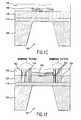
- FIGS. 1A through 1Gare schematic cross-sectional views illustrating one embodiment of a MEMS membrane fabrication sequence according to the present invention
- FIG. 2is a perspective view of a singulated MEMS membrane device that has been fabricated according to the present invention
- FIG. 3is a schematic cross-sectional view illustrating use of the MEMS membrane in a Fabry-Perot tunable filter
- FIGS. 4A and 4Bare schematic cross-sectional views illustrating another embodiment of a MEMS membrane fabrication sequence according to the present invention.
- FIGS. 5A through 5Care schematic cross-sectional views illustrating still another embodiment of a MEMS membrane fabrication sequence according to the present invention.
- FIGS. 6A and 6Bare schematic cross-sectional views illustrating a fourth embodiment of a MEMS membrane fabrication sequence according to the present invention.
- FIGS. 7A and 7Bare schematic cross-sectional views illustrating a fifth embodiment of a MEMS membrane fabrication sequence according to the present invention.
- FIG. 8is schematic cross-sectional view illustrating a sixth embodiment of a MEMS membrane fabrication sequence according to the present invention.
- FIGS. 1A through 1Gillustrate a process for fabricating a MEMS deflectable structure, such as a membrane, with an optical coating, which utilizes principles of the present invention.
- the processbegins with a support such as a handle wafer 100 , which in one embodiment is a standard n-type doped silicon wafer.
- the handle wafer 100is 75 mm to 150 mm in diameter and is 400 to 500 microns thick in one implementation.
- a sacrificial layer 110is formed on the wafer 100 through oxidization, for example.
- This sacrificial layer 110has a depth of typically less than 10 micrometers ( ⁇ m), 2 to 5 ⁇ m in one example.
- the device layer 125is deposited or installed on the sacrificial layer 110 .
- the device layer 125is typically greater than 5 ⁇ m. Currently, it is between 6 to 10 ⁇ m in thickness.
- the device layeris a polysilicon layer that is deposited in a low-pressure chemical vapor deposition process.
- a dopant, such as n-type,is preferably added to improve conductivity while controlling the crystallinity and density of the polysilicon.
- silicon wafer materialis used as the device layer. In a wafer bonding process, a silicon device layer 125 is bonded to the oxide layer 110 using elevated temperature and pressure.
- the device layer 125is annealed and polished back to the desired membrane thickness, if required.
- an optical port 101is patterned and etched into the backside of the handle or support wafer 100 , preferably using a combination of isotropic and anisotropic etching.
- the sacrificial oxide layer 110is used as an etch stop.
- the optical port etch stepcan be omitted, as silicon is partially transparent at infrared wavelengths, in which case an anti-reflective (AR) coating is applied to the outer surface of handle wafer 100 to minimize reflection from the air-silicon interface.
- ARanti-reflective
- a depression 130is formed in the front side of the device layer 125 . This depression is used to form a curved mirror structure.
- FIG. 1Cshows the deposition of a multi layer, thin film dielectric coating 140 .
- the coatingis highly reflective (HR), i.e., has a reflectivity of greater than 98%. In another example, the coating has a lower reflectivity of 30% to 98% for example.
- the dielectric coatingis chosen, however, over gold, aluminum, or other metals, for example because of its low loss characteristics.
- the dielectric coatingfunctions as a dichroic filter, such as a WDM filter, that selectively transmits and reflects specific wavelength bands.
- the dielectric coating 140is an HR coating having preferably 4 or more quarterwave layers, preferably 8 or more, with a 16 dielectric layer mirror being used in some implementations.
- a mask layer 145is deposited over the dielectric coating 140 .
- FIG. 1Dshows the patterning of the mask layer 145 .
- a positive or negative photoresistis used, which is developed so that the remainder of the mask layer 145 resides in an optical port region that surrounds an optical axis 2 of the device. This is located over the optical port 101 , if present.
- the remainder of the mask layer 145is used as an etch protection layer during a subsequent etch of the dielectric coating 140 , thus yielding the patterned dielectric coating 140 of the figure.
- the preferred method for etching the dielectric coatings 140is to use a dry etch process, such as reactive ion etching and reactive ion milling. Films with a thickness of 3 to 4 ⁇ m have been etched with a photoresist mask, provided adequate backside cooling is employed.
- the etch chemistrycan be based on CHF3/CF4/Ar. Ion beam milling is an alternative, but the etch times for this process are typically much longer.
- FIG. 1Eshows the deposition of membrane mask/patterned dielectric protection layer 150 , which is used in the patterning of the device layer 125 .
- FIG. 1Fshows development of the membrane mask/patterned dielectric protection layer 150 with the membrane and tether patterns. These patterns are transferred into the device layer 125 . Voids 152 and 154 are formed in the device layer 125 to define the tethers 158 of the membrane, along with release holes 232 .
- the membrane mask layer 125functions to protect the dielectric coating 140 from the etchants used to attack the exposed regions of the device layer.
- FIG. 1Gshows the device after the release process.
- a portion of the sacrificial layer 110is removed by a wet oxide etch process to “release” the membrane and tether structure from the sacrificial oxide layer 110 and handle wafer 100 .
- a buffered HF etch, followed by methanol, followed by a drying step using supercritical carbon dioxideis used.
- the etchantattacks the release layer from the backside through the optical port 101 and the front side through the voids 152 , 154 and release holes 232 .
- the dielectric coating 140is entirely encapsulated between the protection layer 150 and the device layer 125 . Protection of the dielectric coating 140 during release is required since materials such as silicon dioxide, titanium dioxide and tantalum pentoxide are etched by hydrofluoric acid. Preferably, a buffered etch is also used to preserve the protection layer 150 , especially if a photoresist material is used.
- Another protection schemeis to deposit a mask layer that functions as a protection mask as well as be incorporated into the overall optical function of the coating, eliminating the need to remove the mask layer after release.
- two candidate materialsare amorphous silicon or silicon nitride.
- the dielectric filmis deposited conformally over the surface; but the coating design is adjusted in anticipation of an additional layer.
- the featuresare etched using the dry etch process as before.
- An additional conformal layeris then deposited over the entire surface of the wafer.
- Sputtering or a plasma enhanced chemical vapor deposition (PECVD) systemsprovide the best conformal coverage.
- PECVDplasma enhanced chemical vapor deposition
- an e-beam evaporator with a planetary systemis an alternative.
- the optical design of the coatingis tailored so that its performance was not sensitive to the thickness of this last layer, eliminating the need for precise control of the deposition rate.
- This final mask layeris patterned using a dry or wet etch process if it were desirable to reduce the area over which it extended. For example, it may be necessary to reduce the area to that immediately surrounding the dielectric coating so that it does not influence the mechanical properties of the MEMS structure.
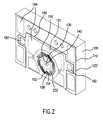
- FIG. 2shows the completed MEMS device.
- An exemplary membrane-tether configurationis shown.
- the patterned membrane layer 125 ′comprises a center body portion 156 that is aligned over the optical port 101 (shown in phantom) and tethers 158 formed by the removal of the device layer from voids or regions 152 , 154 .
- An isolation trench 186 through at least the device layer 125 ′prevents shorting of the handle and device layers due to edge damage.
- FIG. 3shows the deployment of the MEMS device in Fabry-Perot filter 10 . Specifically, it is paired with a mirror to form a FP cavity 18 .
- the filter 10includes mirror device 16 and a spacer layer 17 that separates the mirror device from the MEMS membrane.
- the mirror device 16includes a dielectric mirror coating 19 that is preferably matched to the membrane's dielectric coating 140 in reflectivity.
- These functional layersare held together and operated as a tunable FP filter by modulating voltage between the handle wafer 100 and the membrane 125 ′.
- An anti-reflection (AR) coating 105is preferably deposited through the optical port 101 onto the exterior surface of the membrane layer 125 ′.
- the curved mirroris located on the membrane.
- the curved surfaceis located on the mirror device.
- the advantage to the placement on the membraneconcerns the ability to manufacture the mirror device integrated with the spacer using SOI material, for example.
- both mirrorsare flat to form a flat—flat cavity.
- FIGS. 4A and 4Billustrate an alternative process for protecting the dielectric coating 140 during the release process, specifically after the membrane layer 125 ′ has been patterned and the dielectric coating 140 has been patterned.
- This alternative processbegins with the device illustrated in FIG. 1F, with resist 150 stripped.
- a resist smoothing layer 168is deposited to cover and encapsulate the patterned dielectric coating 140 .
- a lift-off resist 160 and possibly a second resist 164are deposited to cover the topography of the patterned membrane layer 125 ′, the topography being for example, the etch holes 232 and voids 152 , 154 defining the tethers 158 .
- this protection layer 162is a metal, such as nickel or gold, for example.
- a sputtering systemis preferred.
- the smoothing layer 168may not be needed, depending on the profile of coating 140 and sputtering coverage.
- the lift-off resistis removed, leaving the protection layer 162 encapsulating the dielectric coating 140 .
- a non-buffered HF acid release processcan be performed to remove the portion of the sacrificial layer underneath the membrane 156 in the release process.
- the protection layer 162is stripped after release using, for example, a wet etch step.
- FIGS. 5A-5Bshow another process flow.
- a first smoothing layer 168such as a resist, is used to cover and smooth the sensitive topography of the dielectric coating 140 and also provide an ancillary barrier to the HF acid or other release etchant.
- a membrane mask/patterned dielectric protection layer 162is applied that is both impervious to the release acid and is also a good masking material for the membrane topography.
- a metalsuch as gold or nickel, is used in one implementation.
- the protection masking layer 162is then patterned with the membrane pattern as illustrated in FIG. 5 B. The pattern is transferred to yield the patterned membrane layer 125 ′.
- the release processis performed with the protection layer 162 preserving the coating 140 , after which the masking protection layer 162 and the photoresist layer 168 are removed.
- FIGS. 6A and 6Billustrate a modification in which the protection masking layer 162 is etched back prior to membrane release.
- a protection layer patterning photoresist 170is deposited and the metal protection layer 162 is removed from the membrane topography, specifically, uncovering the areas where the release etchant must be allowed to reach the sacrificial layer 110 .
- the release processis performed.
- FIGS. 7A and 7Billustrate a process flow in which the release of the MEMS structure is partially or completely performed prior to the deposition and patterning of the dielectric coating.
- a membrane topography protection layer 160is deposited outside of the optical port region of a released or partially released membrane structure 156 .
- a thick lift-off resistis preferably used.
- the voids or regions 152 , 154 and the etchant holes 232are covered.
- a second photoresist layer 164can be applied and patterned.
- the dielectric coating 140is deposited over the front side followed by a resist mask layer 145 that is patterned to reside in the optical port region.
- the exposed dielectric coating 140is then etched back to form the illustrated structure.
- the resist mask 145is then removed.
- FIG. 8illustrates still another option in which the lift-off resist topography protection layer 160 is used to as a mask to pattern the dielectric coating 140 . Specifically, the dielectric coating is deposited into optical port region and on top of the lift-off resist 160 . The excess dielectric is removed with resist 160 .
- a difficulty with these embodimentsis resist survival in the elevated temperatures required in the dielectric coating process.
- the optical portis patterned into the backside of the wafer prior to the deposition of the dielectric film on the front side, in some cases. Executing this step prior to depositing the optical coatings is not necessary.
- the dielectriccould be applied to a plain SOI wafer and patterned prior to etching the optical port. The protection methods would be essentially unchanged.
- the point at which the dielectric film is patternedcould be adjusted to optimize the overall process flow.
Landscapes
- Physics & Mathematics (AREA)
- Engineering & Computer Science (AREA)
- Microelectronics & Electronic Packaging (AREA)
- Spectroscopy & Molecular Physics (AREA)
- General Physics & Mathematics (AREA)
- Optics & Photonics (AREA)
- Manufacturing & Machinery (AREA)
- Computer Hardware Design (AREA)
- Mechanical Light Control Or Optical Switches (AREA)
- Micromachines (AREA)
- Optical Integrated Circuits (AREA)
Abstract
Description
Claims (26)
Priority Applications (3)
| Application Number | Priority Date | Filing Date | Title |
|---|---|---|---|
| US09/954,861US6790698B2 (en) | 2000-10-19 | 2001-09-18 | Process for integrating dielectric optical coatings into micro-electromechanical devices |
| PCT/US2001/032512WO2002033458A2 (en) | 2000-10-19 | 2001-10-17 | Process for integrating dielectric optical coatings into microelectromechanical devices |
| AU2002224426AAU2002224426A1 (en) | 2000-10-19 | 2001-10-17 | Process for integrating dielectric optical coatings into microelectromechanical devices |
Applications Claiming Priority (3)
| Application Number | Priority Date | Filing Date | Title |
|---|---|---|---|
| US09/692,639US6271052B1 (en) | 2000-10-19 | 2000-10-19 | Process for integrating dielectric optical coatings into micro-electromechanical devices |
| US90785601A | 2001-07-18 | 2001-07-18 | |
| US09/954,861US6790698B2 (en) | 2000-10-19 | 2001-09-18 | Process for integrating dielectric optical coatings into micro-electromechanical devices |
Related Parent Applications (1)
| Application Number | Title | Priority Date | Filing Date |
|---|---|---|---|
| US90785601AContinuation | 2000-10-19 | 2001-07-18 |
Publications (2)
| Publication Number | Publication Date |
|---|---|
| US20020048839A1 US20020048839A1 (en) | 2002-04-25 |
| US6790698B2true US6790698B2 (en) | 2004-09-14 |
Family
ID=27418563
Family Applications (1)
| Application Number | Title | Priority Date | Filing Date |
|---|---|---|---|
| US09/954,861Expired - LifetimeUS6790698B2 (en) | 2000-10-19 | 2001-09-18 | Process for integrating dielectric optical coatings into micro-electromechanical devices |
Country Status (3)
| Country | Link |
|---|---|
| US (1) | US6790698B2 (en) |
| AU (1) | AU2002224426A1 (en) |
| WO (1) | WO2002033458A2 (en) |
Cited By (7)
| Publication number | Priority date | Publication date | Assignee | Title |
|---|---|---|---|---|
| US20030178075A1 (en)* | 2002-02-12 | 2003-09-25 | Kionix, Inc. | Fabrication of ultra-shallow channels for microfluidic devices and systems |
| US20040075364A1 (en)* | 2002-10-21 | 2004-04-22 | Hrl Laboratories, Llc | Piezoelectric actuator for tunable electronic components |
| US20050127792A1 (en)* | 2002-10-21 | 2005-06-16 | Hrl Laboratories, Llc | Piezoelectric switch for tunable electronic components |
| US20050155851A1 (en)* | 2002-10-21 | 2005-07-21 | Hrl Laboratories, Llc. | Variable capacitance membrane actuator for wide band tuning of microstrip resonators and filters |
| US20060228869A1 (en)* | 2005-04-11 | 2006-10-12 | Hewlett-Packard Development Company, L.P. Intellectual Property Administration | MEMS packaging structure and methods |
| US20060234412A1 (en)* | 2005-04-19 | 2006-10-19 | Hewlett-Packard Development Company, L.P. Intellectual Property Administration | MEMS release methods |
| US7209657B1 (en)* | 2001-12-03 | 2007-04-24 | Cheetah Omni, Llc | Optical routing using a star switching fabric |
Families Citing this family (12)
| Publication number | Priority date | Publication date | Assignee | Title |
|---|---|---|---|---|
| US6891655B2 (en)* | 2003-01-02 | 2005-05-10 | Micronic Laser Systems Ab | High energy, low energy density, radiation-resistant optics used with micro-electromechanical devices |
| US7851333B2 (en)* | 2007-03-15 | 2010-12-14 | Infineon Technologies Ag | Apparatus comprising a device and method for producing it |
| US8334984B2 (en)* | 2008-08-22 | 2012-12-18 | The Regents Of The University Of California | Single wafer fabrication process for wavelength dependent reflectance for linear optical serialization of accelerometers |
| US9078063B2 (en) | 2012-08-10 | 2015-07-07 | Knowles Electronics, Llc | Microphone assembly with barrier to prevent contaminant infiltration |
| US9291740B2 (en)* | 2013-06-12 | 2016-03-22 | Halliburton Energy Services, Inc. | Systems and methods for downhole electric field measurement |
| EP3367082A1 (en) | 2013-11-06 | 2018-08-29 | Invensense, Inc. | Pressure sensor |
| EP2871455B1 (en) | 2013-11-06 | 2020-03-04 | Invensense, Inc. | Pressure sensor |
| EP3614115B1 (en) | 2015-04-02 | 2024-09-11 | InvenSense, Inc. | Pressure sensor |
| US11225409B2 (en) | 2018-09-17 | 2022-01-18 | Invensense, Inc. | Sensor with integrated heater |
| US11326972B2 (en) | 2019-05-17 | 2022-05-10 | Invensense, Inc. | Pressure sensor with improve hermeticity |
| NL2023917B1 (en)* | 2019-09-30 | 2021-05-27 | Univ Delft Tech | High-selectivity dry release of dielectric structures |
| NL2036143B1 (en) | 2023-10-27 | 2025-05-12 | Univ Delft Tech | Broadband, low-mass, and high-reflectivity metasurface-enhanced photonic crystal reflector |
Citations (11)
| Publication number | Priority date | Publication date | Assignee | Title |
|---|---|---|---|---|
| EP0689078A1 (en) | 1994-06-21 | 1995-12-27 | Matsushita Electric Industrial Co., Ltd. | Diffractive optical modulator and method for producing the same |
| EP0788005A2 (en) | 1996-02-01 | 1997-08-06 | AT&T Corp. | Micromechanical optical modulator and method for making the same |
| WO1999034484A2 (en) | 1997-12-29 | 1999-07-08 | Coretek, Inc. | Microelectromechanically, tunable, confocal, vcsel and fabry-perot filter |
| US5949571A (en) | 1998-07-30 | 1999-09-07 | Lucent Technologies | Mars optical modulators |
| US5959516A (en)* | 1998-01-08 | 1999-09-28 | Rockwell Science Center, Llc | Tunable-trimmable micro electro mechanical system (MEMS) capacitor |
| US5963788A (en) | 1995-09-06 | 1999-10-05 | Sandia Corporation | Method for integrating microelectromechanical devices with electronic circuitry |
| US6174820B1 (en) | 1999-02-16 | 2001-01-16 | Sandia Corporation | Use of silicon oxynitride as a sacrificial material for microelectromechanical devices |
| US6178284B1 (en) | 1998-09-30 | 2001-01-23 | Lucent Technologies, Inc. | Variable single-mode attenuators by spatial interference |
| US6271052B1 (en)* | 2000-10-19 | 2001-08-07 | Axsun Technologies, Inc. | Process for integrating dielectric optical coatings into micro-electromechanical devices |
| US6351577B1 (en)* | 1998-12-14 | 2002-02-26 | Lucent Technologies Inc. | Surface-micromachined out-of-plane tunable optical filters |
| US6379989B1 (en)* | 1998-12-23 | 2002-04-30 | Xerox Corporation | Process for manufacture of microoptomechanical structures |
- 2001
- 2001-09-18USUS09/954,861patent/US6790698B2/ennot_activeExpired - Lifetime
- 2001-10-17WOPCT/US2001/032512patent/WO2002033458A2/enactiveApplication Filing
- 2001-10-17AUAU2002224426Apatent/AU2002224426A1/ennot_activeAbandoned
Patent Citations (11)
| Publication number | Priority date | Publication date | Assignee | Title |
|---|---|---|---|---|
| EP0689078A1 (en) | 1994-06-21 | 1995-12-27 | Matsushita Electric Industrial Co., Ltd. | Diffractive optical modulator and method for producing the same |
| US5963788A (en) | 1995-09-06 | 1999-10-05 | Sandia Corporation | Method for integrating microelectromechanical devices with electronic circuitry |
| EP0788005A2 (en) | 1996-02-01 | 1997-08-06 | AT&T Corp. | Micromechanical optical modulator and method for making the same |
| WO1999034484A2 (en) | 1997-12-29 | 1999-07-08 | Coretek, Inc. | Microelectromechanically, tunable, confocal, vcsel and fabry-perot filter |
| US5959516A (en)* | 1998-01-08 | 1999-09-28 | Rockwell Science Center, Llc | Tunable-trimmable micro electro mechanical system (MEMS) capacitor |
| US5949571A (en) | 1998-07-30 | 1999-09-07 | Lucent Technologies | Mars optical modulators |
| US6178284B1 (en) | 1998-09-30 | 2001-01-23 | Lucent Technologies, Inc. | Variable single-mode attenuators by spatial interference |
| US6351577B1 (en)* | 1998-12-14 | 2002-02-26 | Lucent Technologies Inc. | Surface-micromachined out-of-plane tunable optical filters |
| US6379989B1 (en)* | 1998-12-23 | 2002-04-30 | Xerox Corporation | Process for manufacture of microoptomechanical structures |
| US6174820B1 (en) | 1999-02-16 | 2001-01-16 | Sandia Corporation | Use of silicon oxynitride as a sacrificial material for microelectromechanical devices |
| US6271052B1 (en)* | 2000-10-19 | 2001-08-07 | Axsun Technologies, Inc. | Process for integrating dielectric optical coatings into micro-electromechanical devices |
Non-Patent Citations (5)
| Title |
|---|
| Aratani, K., et al., "Surface micromachined tuneable interferometer array." XP-000454081. pp. 17-23. |
| Ayazi, Farrokh; Najafi, Khalil, "High Aspect-Ratio Combined Poly and Single-Crystal Silicon (HARPSS) MEMS Technology," Journal of Microelectromechanical Systems, vol. 9, No. 3 Sep. 3, 2000, pp. 288-294. |
| Dichroic Filter Array(TM) Patent Patterned Coatings Technology, Ocean Optics, Inc., http://www.oceanotics.com/products/dfa.asp. |
| Dichroic Filter Array™ Patent Patterned Coatings Technology, Ocean Optics, Inc., http://www.oceanotics.com/products/dfa.asp. |
| Jerman, J.II., et al., "A Miniature Fabry-Perot Interferometer Fabricated Using Silicon Micromachining Techniques." XP-10079190A. pp. 16-18. |
Cited By (17)
| Publication number | Priority date | Publication date | Assignee | Title |
|---|---|---|---|---|
| US7209657B1 (en)* | 2001-12-03 | 2007-04-24 | Cheetah Omni, Llc | Optical routing using a star switching fabric |
| US20030178075A1 (en)* | 2002-02-12 | 2003-09-25 | Kionix, Inc. | Fabrication of ultra-shallow channels for microfluidic devices and systems |
| US7171975B2 (en)* | 2002-02-12 | 2007-02-06 | Kionix, Inc. | Fabrication of ultra-shallow channels for microfluidic devices and systems |
| US20050155851A1 (en)* | 2002-10-21 | 2005-07-21 | Hrl Laboratories, Llc. | Variable capacitance membrane actuator for wide band tuning of microstrip resonators and filters |
| US7215064B2 (en) | 2002-10-21 | 2007-05-08 | Hrl Laboratories, Llc | Piezoelectric switch for tunable electronic components |
| US7992271B2 (en) | 2002-10-21 | 2011-08-09 | Hrl Laboratories, Llc | Process of manufacturing a piezoelectric actuator for tunable electronic components on a carrier substrate |
| US20100064493A1 (en)* | 2002-10-21 | 2010-03-18 | Hrl Laboratories, Llc | Piezoelectric actuator for tunable electronic components |
| US7161791B2 (en)* | 2002-10-21 | 2007-01-09 | Hrl Laboratories, Llc | Variable capacitance membrane actuator for wide band tuning of microstrip resonators and filters |
| US20050127792A1 (en)* | 2002-10-21 | 2005-06-16 | Hrl Laboratories, Llc | Piezoelectric switch for tunable electronic components |
| US20040075364A1 (en)* | 2002-10-21 | 2004-04-22 | Hrl Laboratories, Llc | Piezoelectric actuator for tunable electronic components |
| US20050151444A1 (en)* | 2002-10-21 | 2005-07-14 | Hrl Laboratories, Llc | Piezoelectric switch for tunable electronic components |
| US7656071B2 (en) | 2002-10-21 | 2010-02-02 | Hrl Laboratories, Llc | Piezoelectric actuator for tunable electronic components |
| US7343655B2 (en) | 2002-10-21 | 2008-03-18 | Hrl Laboratories, Llc | Manufacturing methods of micro electromechanical switch |
| US7400488B2 (en) | 2002-10-21 | 2008-07-15 | Hrl Laboratories, Llc | Variable capacitance membrane actuator for wide band tuning of microstrip resonators and filters |
| US7288464B2 (en) | 2005-04-11 | 2007-10-30 | Hewlett-Packard Development Company, L.P. | MEMS packaging structure and methods |
| US20060228869A1 (en)* | 2005-04-11 | 2006-10-12 | Hewlett-Packard Development Company, L.P. Intellectual Property Administration | MEMS packaging structure and methods |
| US20060234412A1 (en)* | 2005-04-19 | 2006-10-19 | Hewlett-Packard Development Company, L.P. Intellectual Property Administration | MEMS release methods |
Also Published As
| Publication number | Publication date |
|---|---|
| AU2002224426A1 (en) | 2002-04-29 |
| US20020048839A1 (en) | 2002-04-25 |
| WO2002033458A2 (en) | 2002-04-25 |
| WO2002033458A3 (en) | 2003-08-14 |
Similar Documents
| Publication | Publication Date | Title |
|---|---|---|
| US6790698B2 (en) | Process for integrating dielectric optical coatings into micro-electromechanical devices | |
| US6271052B1 (en) | Process for integrating dielectric optical coatings into micro-electromechanical devices | |
| US6768756B2 (en) | MEMS membrane with integral mirror/lens | |
| US7968986B2 (en) | Lid structure for microdevice and method of manufacture | |
| US6608711B2 (en) | Silicon on insulator optical membrane structure for fabry-perot MOEMS filter | |
| US7268081B2 (en) | Wafer-level transfer of membranes with gas-phase etching and wet etching methods | |
| US6808276B2 (en) | Suspended high reflectivity coating on release structure and fabrication process therefor | |
| EP0683921B1 (en) | Microstructures and single mask, single-crystal process for fabrication thereof | |
| US20060196843A1 (en) | Process for fabricating monolithic membrane substrate structures with well-controlled air gaps | |
| US6538798B2 (en) | Process for fabricating stiction control bumps on optical membrane via conformal coating of etch holes | |
| CN103262207A (en) | Multi-layer substrate structure and manufacturing method for the same | |
| EP1213259B1 (en) | Process for manufacturing micromechanical and microoptomechanical structures with single crystal silicon exposure step | |
| US6721098B2 (en) | Triple electrode MOEMS tunable filter and fabrication process therefor | |
| US7567375B2 (en) | Hidden hinge MEMS device | |
| US6777258B1 (en) | Conductive etch stop for etching a sacrificial layer | |
| US6707593B2 (en) | System and process for actuation voltage discharge to prevent stiction attachment in MEMS device | |
| US6765710B2 (en) | Interference tabs for avoiding snapdown of optical membrane and fabrication process | |
| WO2002033469A2 (en) | Fabrication process for polysilicon deflectable membrane | |
| US20020028394A1 (en) | Method for manufacturing a membrane mask | |
| TW202430467A (en) | Mems tensioning structures and methods of manufacture |
Legal Events
| Date | Code | Title | Description |
|---|---|---|---|
| AS | Assignment | Owner name:AXSUN TECHNOLOGIES, INC., MASSACHUSETTS Free format text:ASSIGNMENT OF ASSIGNORS INTEREST;ASSIGNORS:MILLER, MICHAEL F.;LE, MINH VAN;COOK, CHRISTOPHER C.;AND OTHERS;REEL/FRAME:012182/0479;SIGNING DATES FROM 20010827 TO 20010910 | |
| STCF | Information on status: patent grant | Free format text:PATENTED CASE | |
| FPAY | Fee payment | Year of fee payment:4 | |
| FEPP | Fee payment procedure | Free format text:PAT HOLDER NO LONGER CLAIMS SMALL ENTITY STATUS, ENTITY STATUS SET TO UNDISCOUNTED (ORIGINAL EVENT CODE: STOL); ENTITY STATUS OF PATENT OWNER: SMALL ENTITY | |
| FPAY | Fee payment | Year of fee payment:8 | |
| FEPP | Fee payment procedure | Free format text:PAT HOLDER CLAIMS SMALL ENTITY STATUS, ENTITY STATUS SET TO SMALL (ORIGINAL EVENT CODE: LTOS); ENTITY STATUS OF PATENT OWNER: SMALL ENTITY | |
| AS | Assignment | Owner name:AXSUN TECHNOLOGIES LLC, MASSACHUSETTS Free format text:CHANGE OF NAME;ASSIGNOR:AXSUN TECHNOLOGIES, INC.;REEL/FRAME:037901/0152 Effective date:20151015 | |
| FPAY | Fee payment | Year of fee payment:12 | |
| AS | Assignment | Owner name:AXSUN TECHNOLOGIES, INC., MASSACHUSETTS Free format text:CHANGE OF NAME;ASSIGNOR:AXSUN TECHNOLOGIES, LLC;REEL/FRAME:043733/0195 Effective date:20160329 | |
| AS | Assignment | Owner name:ROYAL BANK OF CANADA, AS COLLATERAL AGENT, NEW YORK Free format text:SECOND LIEN INTELLECTUAL PROPERTY SECURITY AGREEMENT;ASSIGNOR:AXSUN TECHNOLOGIES, INC.;REEL/FRAME:048000/0711 Effective date:20190102 Owner name:JPMORGAN CHASE BANK, N.A., NEW YORK Free format text:FIRST LIEN INTELLECTUAL PROPERTY SECURITY AGREEMENT;ASSIGNOR:AXSUN TECHNOLOGIES, INC.;REEL/FRAME:048000/0692 Effective date:20190102 Owner name:ROYAL BANK OF CANADA, AS COLLATERAL AGENT, NEW YOR Free format text:SECOND LIEN INTELLECTUAL PROPERTY SECURITY AGREEMENT;ASSIGNOR:AXSUN TECHNOLOGIES, INC.;REEL/FRAME:048000/0711 Effective date:20190102 | |
| AS | Assignment | Owner name:AXSUN TECHNOLOGIES, INC., MASSACHUSETTS Free format text:RELEASE OF SECOND LIEN SECURITY INTEREST IN INTELLECTUAL PROPERTY;ASSIGNOR:ROYAL BANK OF CANADA, AS COLLATERAL AGENT;REEL/FRAME:061161/0942 Effective date:20220811 Owner name:AXSUN TECHNOLOGIES, INC., MASSACHUSETTS Free format text:RELEASE OF FIRST LIEN SECURITY INTEREST IN INTELLECTUAL PROPERTY;ASSIGNOR:JPMORGAN CHASE BANK, N.A., AS COLLATERAL AGENT;REEL/FRAME:061161/0854 Effective date:20220811 |