US6788335B2 - Pulsed illumination signal modulation control & adjustment method and system - Google Patents
Pulsed illumination signal modulation control & adjustment method and systemDownload PDFInfo
- Publication number
- US6788335B2 US6788335B2US09/746,859US74685900AUS6788335B2US 6788335 B2US6788335 B2US 6788335B2US 74685900 AUS74685900 AUS 74685900AUS 6788335 B2US6788335 B2US 6788335B2
- Authority
- US
- United States
- Prior art keywords
- light source
- sensor
- film
- output
- response
- Prior art date
- Legal status (The legal status is an assumption and is not a legal conclusion. Google has not performed a legal analysis and makes no representation as to the accuracy of the status listed.)
- Expired - Fee Related, expires
Links
Images


Classifications
- H—ELECTRICITY
- H04—ELECTRIC COMMUNICATION TECHNIQUE
- H04N—PICTORIAL COMMUNICATION, e.g. TELEVISION
- H04N1/00—Scanning, transmission or reproduction of documents or the like, e.g. facsimile transmission; Details thereof
- H04N1/00127—Connection or combination of a still picture apparatus with another apparatus, e.g. for storage, processing or transmission of still picture signals or of information associated with a still picture
- H04N1/00249—Connection or combination of a still picture apparatus with another apparatus, e.g. for storage, processing or transmission of still picture signals or of information associated with a still picture with a photographic apparatus, e.g. a photographic printer or a projector
- H04N1/00267—Connection or combination of a still picture apparatus with another apparatus, e.g. for storage, processing or transmission of still picture signals or of information associated with a still picture with a photographic apparatus, e.g. a photographic printer or a projector with a viewing or projecting apparatus, e.g. for reading image information from a film
- H—ELECTRICITY
- H04—ELECTRIC COMMUNICATION TECHNIQUE
- H04N—PICTORIAL COMMUNICATION, e.g. TELEVISION
- H04N1/00—Scanning, transmission or reproduction of documents or the like, e.g. facsimile transmission; Details thereof
- H04N1/00795—Reading arrangements
- H—ELECTRICITY
- H04—ELECTRIC COMMUNICATION TECHNIQUE
- H04N—PICTORIAL COMMUNICATION, e.g. TELEVISION
- H04N1/00—Scanning, transmission or reproduction of documents or the like, e.g. facsimile transmission; Details thereof
- H04N1/00795—Reading arrangements
- H04N1/00798—Circuits or arrangements for the control thereof, e.g. using a programmed control device or according to a measured quantity
- H04N1/00816—Determining the reading area, e.g. eliminating reading of margins
- H—ELECTRICITY
- H04—ELECTRIC COMMUNICATION TECHNIQUE
- H04N—PICTORIAL COMMUNICATION, e.g. TELEVISION
- H04N1/00—Scanning, transmission or reproduction of documents or the like, e.g. facsimile transmission; Details thereof
- H04N1/40—Picture signal circuits
- H04N1/40056—Circuits for driving or energising particular reading heads or original illumination means
- H—ELECTRICITY
- H04—ELECTRIC COMMUNICATION TECHNIQUE
- H04N—PICTORIAL COMMUNICATION, e.g. TELEVISION
- H04N1/00—Scanning, transmission or reproduction of documents or the like, e.g. facsimile transmission; Details thereof
- H04N1/40—Picture signal circuits
- H04N1/407—Control or modification of tonal gradation or of extreme levels, e.g. background level
- H04N1/4076—Control or modification of tonal gradation or of extreme levels, e.g. background level dependent on references outside the picture
- H—ELECTRICITY
- H04—ELECTRIC COMMUNICATION TECHNIQUE
- H04N—PICTORIAL COMMUNICATION, e.g. TELEVISION
- H04N2201/00—Indexing scheme relating to scanning, transmission or reproduction of documents or the like, and to details thereof
- H04N2201/04—Scanning arrangements
- H04N2201/0402—Arrangements not specific to a particular one of the scanning methods covered by groups H04N1/04 - H04N1/207
- H04N2201/0404—Scanning transparent media, e.g. photographic film
- H04N2201/0408—Scanning film strips or rolls
Definitions
- This inventionrelates generally to image processing and more particularly to a pulsed illumination signal modulation control and adjustment method and system.
- processing images from filmtypically includes capturing digital data from the film with a sensor as the film is illuminated with a light source. Because the illumination levels captured by the sensor represent the image data, any sensor or illumination non-uniformities introduce undesirable errors into the data measurements.
- sensor and illumination characteristicstypically vary individually and can drift over time due to factors such as heating and/or transient responses in the devices when they are activated and deactivated. Where the film is scanned while being developed, variances in film and chemical developer characteristics often arise due to changes that take place during the development process. Signal levels captured by the sensors may also vary due to factors such as aging of the sensors or light sources.
- a light sourcemay emit one pulse of illumination, during which a sensor may capture data. Any differences in illuminated power between pulses are captured by the sensor, including sensor or illumination characteristics that change during the development process. These differences may be erroneously interpreted as differences in data content captured from the film.
- the present inventionsubstantially reduces or eliminates disadvantages and problems of existing systems.
- One aspect of the inventionis a method for signal modulation adjustment.
- the methodcomprises illuminating a reference target and a region of film with a first light source for a first time interval.
- the methodfurther comprises capturing image data from the film in response to a first amount of light reflected from the film with a first sensor for a first integration time.
- the methodalso comprises approximately simultaneously producing a first reference output in response to a first amount of light reflected from the reference target in a field of view of a reference sensor. More particularly, the method further comprises adjusting the data in response to the reference output.
- the methodcomprises adjusting an output illumination level of the first light source in response to the first reference output before a next time interval.
- the inventionprovides several important advantages. Various embodiments of the invention may have none, some, or all of these advantages.
- the inventionmay improve the accuracy of image data. For example, the invention may compensate for drift or other variations in sensor or illumination source characteristics between image capture sampling times.
- the inventionmay automatically adjust illumination levels and/or sensor integration time using a reference or sensing detector. Signal modulation can be stabilized between illumination pulses, to reduce signal noise.
- the inventionmay also prevent saturation of sensors in varying film, developer, and illumination conditions.
- the inventionmay adjust the captured image data to compensate for such variations.
- sensor and illumination non-uniformities in the image datamay be normalized and various gains for the image data may be adjusted using the measured data.
- FIG. 1illustrates an example of a digital film processing system that may be used in accordance with the invention
- FIG. 1Aillustrates an example of a cross section of film from which image data may be captured
- FIG. 2Aillustrates an example of an image capture engine that comprises an embodiment of the present invention
- FIG. 2Billustrates another example of an image capture engine that comprises another embodiment of the present invention
- FIG. 2Cillustrates another example of an image capture engine that comprises another embodiment of the present invention
- FIG. 3illustrates an example of a method for capturing and adjusting image data in accordance with the present invention.
- FIG. 4illustrates an example of a method for monitoring and adjusting illumination of an image capture system utilizing the teachings of the present invention.
- FIGS. 1-4 of the drawingslike numerals being used for like and corresponding parts of the various drawings.
- Opportunitiesmay be created to detect and/or adjust for sensor and/or illumination variations due to temperature fluctuations and/or other nonuniformities during digital film processing.
- the non-uniformities within a generally linear array of detectorsmay be assumed to drift up or down together between capture of data columns along film while data from the film is being captured.
- a reference targetmay be used to monitor illumination levels as image data is obtained along the film between each imaging window, continually or as desired.
- measured illumination levelsare likely to drift rapidly enough to affect the quality of the image data, they may be monitored. Then, image data may be adjusted in response to these levels as they change between data columns. This information may also be used to adjust signal modulation before a selected imaging window. This may desirably allow digital film processing to be performed independently of content and/or unexposed regions within the film. It may also ensure that illumination is generally uniform or varies within a small range between each imaging window. The accuracy of captured image data may be desirably improved by compensating for these variations over time. In addition, these adjustments may also accommodate variations in the elevation and density of developing chemicals applied to the film as the film develops.
- FIG. 1illustrates an example of a digital film processing system 10 that comprises an embodiment of the present invention.
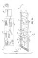
- Digital film processing system 10comprises a film dispenser 22 , at least one transport mechanism 23 , a developer station 24 , a processor 36 and at least one input/output device 25 , and at least one sensor station 40 .
- Digital film processing system 10is operable to capture and/or adjust data captured from a film 60 that is disposed proximate to and/or may move at a scan rate relative to sensor station 40 .
- Digital film processing system 10may desirably improve the accuracy of captured image data by compensating for fluctuations in a variety of parameters over time.
- sensor station 40may be disposed in a z direction proximate to, and may be moved at a scan rate relative to, a film 60 operable to store latent image data, such as film.
- Film 60may be disposed, for example, in an x-y plane and have a width W in the y direction.
- film 60may be disposed in a generally vertical orientation, and/or may not be disposed within any single plane, but rather move through a plurality of orientations as sensor station 40 captures image data therefrom.
- film 60may be disposed in a mobius strip configuration so that sensor station 40 may capture image data from both portions 64 and 66 .
- Sensor station 40may also be disposed proximate to and oriented in various angles relative to film 60 .
- At least one sensor station 40is operable to obtain image data from film 60 , even while the film may have developing chemicals applied thereto.
- the filmmay be developing, or may be completely developed.
- Developer station 24may be used to apply a thin layer of a developing chemical to film 60 .
- developer station 24may be a slot coater or vibrating dispenser that sprays or otherwise applies the developing chemical to film 60 .
- Transport mechanism 23may be used to move film 60 at a desired scan rate relative to sensor station 40 .
- Film dispenser 22may be used to retain film 60 and to guide the film onto transport mechanism 23 .
- Sensor station 40may be used to capture image data from film 60 and transfers the image data to an input/output device 25 such as a storage medium.
- Sensor station 40comprises optics 46 , light source 50 , sensor 52 , sensor control 42 , and illumination control 43 .
- Sensor 52operates in concert with light source 50 and optics 46 to capture or obtain image data from a film 60 such as film.
- any suitable light source 50 and compatible sensor 52such as those typically used in image processing applications involving photographic images may be used to capture image data for this aspect of sensor station 40 .
- sensor 52may be any detector whose quantum efficiency, or responsivity, is compatible with a spectrum utilized by light source 50 .
- light source 50comprises mostly infrared or near-infrared energy, or energy outside the visible spectrum
- sensor 52is responsively operational to such wavelengths.
- Such an embodimentmay be advantageous when digital film processing system 10 is used to capture image data from developing film because, for example, unexposed film is typically very reflective when illuminated with infrared energy. Such an advantage may facilitate location of unexposed regions of the film during which updating of estimates may be performed.
- Other combinations of light source and sensorsmay also be used.
- Other examplesmay include, but are not limited to, a light source comprising a single column point source coupled to a scan mirror that may be operated in conjunction with a sensor comprising a point detector coupled to the scan mirror.
- sensor 52may comprise a plurality of charge-coupled devices (CCDs), photo diodes, or CMOS sensors.
- CCDscharge-coupled devices
- sensor 52may comprise a digital camera comprising a two-dimensional array of CCDs operable to capture data from a two-dimensional field of view in film 60 .
- Sensor 52may also comprise a generally linear one-dimensional array, where the array comprises a plurality of detectors such as CCDs.
- Sensor 52may also comprise a generally linear array of 4,096 (or any other number) detectors that may be, for example, staggered or linearly aligned within the array.
- the generally linear arraymay be operable to capture a data or image column over a generally linear field of view that spans width W (in the y direction) of film 60 , or a portion thereof.
- Each detector within sensor 52typically varies in thickness of coating, photoemissive characteristics, optics, etc., and thus typically varies in responsivity to a given amount of illumination.
- the responsivity of each detectoralso varies due to noise, age, and temperature. Such variation in responsivity to illumination within each sensor typically results in spatial non-uniformities in the image data.
- sensor 52comprises a generally linear CCD array
- variations in the efficiency of each detector in converting photons to electronsresults in variations in illumination levels measured by each detector, regardless of variations in the film 60 and/or content therein.
- a system signal-to-noise ratiomay be measured by a combination of sensor responsivity and illumination characteristics of each sensor station. This signal-to-noise ratio may be improved by selecting sensor 52 for its sensitivity to intensity and wavelength illumination. Further improvements to the accuracy of captured data, and thus to image quality, may also be obtained by matching captured electron levels in sensor 52 to a full dynamic range for each latent image within film 60 . For example, the capacity of wells for each detector, that is, the number of photons it may convert to electrons affects the range of discrete digital levels measurable by each detector, regardless of data content within film 60 . Wells within sensor 52 may be desirably sized to be sufficiently large to accommodate desired image signal to noise ratios. In addition, digital film processing system 10 may adjust integration time for sensor 52 and/or adjust the illumination power of light source 50 in order to maximize usage of the capacity of each detector well within sensor 52 .
- light source 50may be arranged in a wave guide.
- Each wave guidemay comprise a plurality of illuminators, such as light emitting diodes (LEDs).
- Lightmay be directed through wave guide 50 to film 60 and then diffusely reflected to sensor 52 .
- Any suitable optics 46 for use with light source 50 and sensor 52may be used to produce desired optical effects in the image captured by sensor 52 .
- optics 46may be used to focus, magnify or enlarge data in film 60 to a desired image resolution for an application, such as 12 ⁇ m per pixel.
- Optics 46 and light source 50may be manually or automatically controlled by, for example, processor 36 .
- Processor 36may be used for image data processing and adjustment in accordance with the present invention. Processor 36 may also control the operation of sensor station 40 by using sensor control 42 and/or illumination control 43 . Alternatively or in addition, processor 36 may control sensor station 40 by, for example, executing software that may be stored in an input/output device 25 such as a storage medium. Although a single input/output device 25 has been illustrated for simplicity, input/output device 25 may comprise multiple storage media as well as comprising storage media of different types. Moreover, although illustrated as separate units, processor 36 may perform some, none, or all of the logic functions described as being performed within illumination control 43 and/or sensor control 42 .
- processor 36may be used to execute applications comprising image data processing and adjustment software. Image data processing and adjustment may be performed using special purpose digital circuitry contained either in processor 36 , or in a separate device. Such dedicated digital circuitry may include, for example, application-specific integrated circuitry (ASIC), state machines, fuzzy logic, etc.
- Processor 36may also comprise a portion of a computer adapted to execute any of the well known MS-DOS, PC-DOS, OS2, UNIX, MAC-OS and Windows operating systems or other operating systems, including nonconventional operating systems.
- Processor 36may comprise random access memory (RAM) 36 a and read only memory (ROM) 36 b , and may be coupled to one or more input/output devices 25 . These devices may include, but are not limited to, printers, disk drives, displays and a communications link.
- Disk drivesmay include a variety of types of storage media such as, for example, floppy disk drives, hard disk drives, CD ROM drives, or magnetic tape drives.
- Input/output device 25comprising a communication link may be connected to a computer network, a telephone line, an antenna, a gateway, or any other type of communication link.
- Image data captured from other than digital film processing system 10may also be adjusted in accordance with the invention.
- processor 36may be coupled to an external network that may be used to obtain image data, such as a scanner or camera system. Captured image data may then be provided to processor 36 from a computer network over the communication link.
- the present inventionincludes programs that may be stored in RAM 36 a , ROM 36 b , or input/output device 25 such as one or more disk drives, and may be executed by processor 36 .
- image data adjustmentmay be performed by software stored and executed by processor 36 with the results stored in an input/output device 25 comprising any suitable storage medium.
- Image datamay be processed as it is obtained, after all data has been captured, or a combination thereof.
- Illumination control 43may be used to control the amount of optical energy given off by light source 50 , both in time and in amplitude. For example, it may be desirable to adjust the output optical energy from light source 50 if sensor 52 is saturating, or if illumination levels are otherwise determined to be too high or too low. Illumination control 43 may also include additional circuitry used to interface the logic with light source 50 .
- Sensor control 42may be used for data transfer and/or processing and to control activation and deactivation of sensor 50 .
- sensor control 42may convert an analog signal to a digital pixel value, or transfer pixel data stored in sensor 52 where sensor 52 has an internal memory.
- sensor 52may also comprise logic, such as a programmable processor, that may adjust or process pixel data as desired, before the pixel data is transferred into a memory or storage medium. Such a processor may perform the functions of sensor control 42 .
- sensor control 42may also include a bias control to improve system dynamic range. For example, sensors may retain residual charge that decreases the amount of usable sensor capacity, for example, in shift registers, a phenomenon known as image lag. Sensor control 42 may desirably increase the system dynamic range by applying a bias to sensor 52 to reduce the effect of this residual scene content on newly captured image data.
- Sensor control 42may comprise software, hardware, or a combination thereof.
- Sensor control 42may also be used to control activation and deactivation of sensor 52 , independently of or in conjunction with light source 50 .
- sensor 52may comprise a mechanical or electronic shutter mechanism for controlling a dwell or integration time in which the sensor may convert a number of photons received into electrons.
- sensor 52integrates over an interval of time signals reflected from film 60 .
- digital film processing system 10may adjust an amount of illumination measurable by sensor 52 and thus system dynamic range as desired.
- Digital film processing system 10may obtain data from many kinds of images, such as color photographic images (either negative print or transparency), black and white images (either negative print or transparency and including black and white images derived from photographic film with multiple layers), other monochromatic images, x-rays, or any other type of image stored on film 60 .
- Digital film processing system 10may capture data from any tangible film 60 that may both reflect back and pass through illumination from a light source.
- One example of film 60is discussed in conjunction with FIG. 1 A.
- FIG. 1Aillustrates an example of a cross-section of film from which image data may be captured.
- Color film 60typically comprises three color emulsion layers—e.g., a blue layer 27 , a green layer 28 and a red layer 29 —that are stacked on an antihalation layer 30 . These four layers are typically stacked on a transparent base substrate layer 31 . Each of these layers and their density affect the incident angle of light transmitted through the film and thus the illumination levels measured by sensor 52 . In some applications, a developing chemical layer 26 may be applied to film 60 .
- Film typesvary with respect to the density of the antihalation layer, layer configuration, and thickness of the base layer.
- the density of filmmay also vary with respect to image content therein.
- photographic filmcontains grains held on a substrate, such as silver-halide, as part of its physical makeup. These grains are a function of the latent image on the film, as well as the type and format of the film, with faster-speed and smaller-format film exhibiting more graininess.
- Developing chemical layer 26may vary in thickness in the z direction between different points on the film, and may also affect the apparent density of the film.
- grains within the film that were exposed to the most lightare the first to develop, and other grains develop as the development process continues. Those areas in which the most grains develop for a given layer will have the greatest density and lowest resultant pixel values. For example, images may contain areas of low-light shadows that contain many more grain traces than areas of bright sky.
- film developsit increases in density as silver is formed from compounds within the film, thus permitting latent images to be obtained by sensor 42 .
- Sensor 52is operable to measure light intensity within a spatial location of an image in film 60 , even while film 60 is developing, or still has developing chemical applied thereto. These measurements may be obtained from silver formed from compounds within film 60 , rather than from dyes within each of layers 27 - 29 after the developing chemical has been removed.
- Each intensity value associated with the intensity of light at that spatial location in the original image in film 60corresponds to one of a series of pixels within an image as captured and/or stored by image capture engine 34 .
- the intensityrefers generally to a pixel's brightness. For example, a white pixel has greater intensity values than a gray or black pixel.
- a black pixeltypically has an intensity value of close to zero, whereas a white pixel has an intensity value of close to 255.
- the range of light intensities within an image on filmmay be referred to as a dynamic range of the image.
- white and dark pixelsas used in this specification is not meant to impart any meaning to the content of image data. For example, white and dark pixels within a film negative would have the opposite meanings for a positive image print.
- FIG. 2Aillustrates an example of an image capture engine that comprises an embodiment of the present invention.
- Image capture engine 34may be a portion of digital film processing system 10 and comprises processor 36 , storage medium 38 and sensor station 40 .
- Image capture engine 34may also capture data from film 60 , including a reference targets 62 and/or 70 and/or a leader 73 .
- Image capture engine 34may utilize reference target 62 to monitor variations in illumination as image data is captured, and/or may adjust signal modulation to respond to such variations.
- Reference target 62is desirably disposed near film 60 and may be imaged with one or more suitably located detectors whose field of view is limited to a portion thereof (reference detectors (not explicitly shown)).
- reference target 70may be disposed so that it blocks or obstructs the field of view of film 60 to detectors within sensor 52 .
- reference target 62may be disposed adjacent to each side of film 60 , or at any sprocket holes therein.
- reference targets 62 and/or 70may be moved into and out of the field of view of the one or more reference sensors at selected times as desired.
- reference target 70 as illustratedmay be moved in a generally y direction into and out of this field of view.
- Any suitable reference targetmay be used that is desirably reasonably and uniformly reflective and/or transmissive of the wavelength of light source 50 , and whose dynamic range is within the expected range of weakest to strongest signals expected from the range in film types.
- Such a reference target 62may desirably reduce the possibility of sensor saturation that may result from gain adjustments of the weakest and/or strongest signals.
- Each of these reference detectors within sensor 52may be used to image reference target 62 and/or 70 through one or more sprocket holes of film 60 or may be moved relative to reference target 62 and/or 70 . Because these reference detectors are subject to similar heating and noise characteristics of image capture engine 34 , they are desirably similar in responsivity and characteristics such as noise, dynamic range, etc. to the detectors within sensor 52 . Such reference detectors also desirably provide a generally true estimate of the energy levels measurable by sensor 52 . One or more of these reference detectors may be included within sensor 52 , or be disposed proximate to sensor 52 . For example, where reference target 62 as illustrated in FIGS.
- 2A-2Cmay be disposed adjacent to each side of film 60 , one or more reference detectors in a generally linear array sensor 52 may be used to capture image data from reference target 62 .
- sensor 52comprises 4096 detectors
- a first plurality of reference detectors representing pixel zero through 128may be used to image a first portion of reference target 62 .
- Detectors 129 through 3966may be used to capture data from film 60
- reference detectors 3967 through 4095may be used to capture data from second portion of reference target 62 .
- Other configurations for reference detectorsmay also be utilized.
- sensor 52may comprise a generally linear array operable to capture a data or image column over a generally linear field of view that spans width W (in the y direction) of film 60 , or a portion thereof.
- Film 60is illustrated with a width W in the y direction measured between a top edge 72 and a bottom edge 74 .
- Film 60may comprise a single image frame I 1 , or a plurality of image frames I 1 -I n disposed along the film in the x direction.
- Each image frame I 1 -I nmay be the same or a different size.
- image frame I 1may be an image represented by a ⁇ b pixels, where a and b are any integer. That is, image I 1 includes a plurality of pixels or columns in the x direction, and b pixels or rows in the y direction.
- a plurality of image frames I 1 -I nis illustrated to discuss one aspect of the invention.
- each of these image frames I 1 -I nmay be separated by an unexposed region R u .
- Some films 60may also include one or more sprocket holes 76 .
- sensor station 40obtains image data from film 60 and transfers the image data to a storage medium such as storage medium 38 .
- Image capture engine 34may create opportunities for monitoring and adjusting signal modulation to accommodate for variations over time and/or due to changes in temperature.
- film 60may comprise an area of unexposed film—the leader 73 —which precedes or trails a plurality of image frames I 1 -I n , in addition to an unexposed region or gutter R u between each image frame I 1 -I n .
- Image capture engine 34may also use some or all of these unexposed regions in the film to provide initial estimates for film characteristics, measurable illumination levels, and/or drift rates.
- image capture engine 34may adjust signal modulation as desired by controlling a combination of illuminated power and sensor integration.
- Signal modulationmay be adjusted by adjusting the pulse width and/or the output amplitude of light source 50 , and/or the integration time of sensor 52 .
- sensor integration timemay be combined, and traded off, with a level of illumination power to obtain an effective illumination time or illumination level that may be captured by a sensor. For example, an increased effective illumination time may be obtained by either increasing sensor integration time at a given illumination power, or increasing the power of illumination at a given sensor integration time. Effective illumination time may be similarly decreased by decreasing sensor integration time or decreasing illuminated power under similar conditions.
- At least one sensing detector 61may be used to measure illumination levels of light source 50 .
- Sensing detector 61may be, for example, a photodiode, and have a field of view restricted to illumination from light source 50 . Any suitable configuration for a sensing detector 61 may be used that provides a reasonably true estimate for the optical power output levels for an integration time during a pulse from light source 50 without capturing additional ambient or reflected light.
- sensing detector 61may be mounted on light source 50 .
- Image capture engine 34may then utilize the sensor, camera and/or illumination drift data measured from the sensing detector 61 and/or reference detectors to adjust image data.
- Illumination control 43may be used to control the amount of optical energy given off by light source 50 , both in time and in amplitude. Illumination control 43 may also comprise logic suitable to respond to readings from sensor 52 or sensing detector 61 , prior readings such as amplitude and/or pulse width from light source 50 , and/or film characteristics. This logic may be software, hardware, or a combination thereof, and may be utilized to, for example, adjust an input current to light source 50 that accordingly adjusts an output optical energy, or illumination level. Illumination control 43 may also comprise additional logic that is operable to accept pulse width control signals from processor 36 as desired. Alternatively or in addition, illumination control 43 may comprise amplitude control logic, which may be software, hardware, or a combination thereof.
- the amplitude control logicmay be responsive to a film type or an operating point, that may be input to or stored in a memory of illumination control 43 , and/or to signal amplitudes of sensors 52 and/or 53 , respectively.
- Illumination control 43may also include additional circuitry used to interface the logic with light source 50 .
- Sensor control 42may also control the dwell or integration time of sensor 52 .
- image capture engine 34may desirably monitor illumination levels and/or adjust signal modulation for expected data within film 60 before capturing image data for each image.
- Image capture engine 34may apply a gain in response to these illumination levels to desirably maximize the dynamic range of the image by mapping intensity values of each location to all usable pixel values (for eight-bit data, there are 256).
- image capture engine 34may utilize one or more of these regions of unexposed film, which comprise a relatively uniform region of the highest light intensities. The adjustment can be made with or without developer on the film. Image capture engine 34 may also use some or all of these unexposed regions to adjust signal modulation and/or to adjust the image data.
- Image capture engine 34may also adjust image data after it has been captured to correct or compensate for these variations that may have been present while the image was captured. Such an advantage may avoid sensor saturation and/or overflow in calculations used to produce the digital image, and improve the quality of the resultant digital image.
- One method for utilizing such an external reference 62 and adjusting signal modulation to achieve desired illumination levelsis illustrated and described in further conjunction with FIG. 4 .
- FIG. 2Billustrates another example of an image capture engine that comprises an embodiment of the present invention.
- Image capture engine 34may also be a portion of digital film processing system 10 and comprises processor 36 , storage medium 38 and sensor stations 40 and 41 .
- Sensor stations 40 and 41may be used to capture image data from film 60 and may be similarly configured, operated and/or controlled.
- sensor station 41may be disposed in a z direction proximate to, and may be moved at a scan rate relative to, film 60 .
- Film 60may also move through a plurality of orientations as both sensor stations 40 and 41 capture image data therefrom.
- Sensor stations 40 and 41may also be disposed proximate to and oriented in various angles relative to film 60 .
- Sensor station 41comprises optics 47 , light source 51 , and sensor 53 , and may also comprise its own sensor and illumination control 48 and 49 . Alternatively, sensor station 41 may share sensor and illumination controls 42 and 43 with sensor station 40 . In this embodiment, sensor station 40 may be located proximate to the top surface 64 of film 60 , and sensor station 41 may be located proximate to bottom surface 66 of film 60 . Sensors 52 and 53 operate in concert with light sources 50 and 51 and optics 46 and 47 to capture or obtain image data from film 60 . Light sources 50 and 51 may utilize the same or different frequencies.
- Sensor station 40 and sensor station 41measure illumination levels through various incident angles of light reflected from and/or passed through film 60 to generate a resultant image.
- sensor 52may be used to capture light from light source 50 reflected from film 60 and/or light from light source 51 illuminated through film 60 .
- sensor 53may be used to capture light from light source 51 reflected from film 60 and/or light from light source 50 illuminated through film 60 .
- Image capture engine 34may later adjust and combine the image data captured from one or more views by sensor stations 40 and/or 41 into various representations of one or more single images.
- Processor 36may control the operation of sensor stations 40 and 41 by using sensor controls 42 and 48 and/or illumination control 43 and 49 .
- processor 36may control sensor stations 40 and/or 41 by, for example, executing software that may be stored in storage medium 38 .
- processor 36may comprise two individual processors. Each of these processors may control a respective sensor station.
- illumination control 49may be used to control the amount of optical energy given off by light source 51 , both in time and in amplitude.
- Sensor controls 42 and 43may be used to control activation and deactivation of sensors 52 and 53 respectively, independently of or in conjunction with light sources 50 and 51 .
- Sensors 52 and 53may integrate over a different intervals of time signals reflected from and transmitted through film 60 from light sources 50 and 51 . Where a given illumination level may be desirable, each sensor 52 and 53 may integrate over a unique interval of time that may vary to capture varying amounts of illuminated power, depending on parameters such as dynamic range or a desired imaging window time.
- Image capture engine 34may thus control a combination of illuminated power and sensor integration time as desired.
- Image capture engine 34is also operable to monitor illumination levels and/or adjust signal modulation as described above.
- an additional sensing detector 61as described in FIG. 2A, may be coupled to or mounted on light source 50 and/or 51 .
- reference detectors, as described in FIG. 2A, associated with sensor stations 40 and 41are each operable to capture energy levels reflected and/or illuminated through reference target 62 and/or 70 from light sources 50 and 51 .
- FIG. 2Cillustrates another example of an image capture engine that comprises an embodiment of the present invention.
- image capture engine 34may also be a portion of digital film processing system 10 and comprises additional sensor stations 40 a and 41 a to monitor the reaction of developing film at one of a plurality of development times for the film. These additional sensor stations may provide additional information with respect to variances in film characteristics as film 60 develops. Any number of additional sensor stations 40 a and 41 a may be used within the scope of the invention.
- sensor stations 40 a and/or 41 amay be disposed proximate to and at various intervals along the x direction of top portion 64 and bottom portion 66 .
- Film 60may move relative to these sensor stations at one or more scan rates where, for example, more than one transport mechanism 23 may be used.
- Each sensor stationmay be controlled with a common processor 36 , or may be controlled with its own processor (not explicitly shown).
- Image capture engine 34may later adjust and combine the image data captured from the plurality of sensor stations 40 and/or 41 into various representations of one or more single images.
- Image capture engine 34is also operable to monitor and/or adjust illumination levels as described above. Additional sensing detectors 61 and/or reference detectors as described in FIGS. 2A and 2B are associated with sensor stations 40 , 40 a , 41 , and 41 b.
- the reflectivity of reference target 62may remain the same or may change from sensor station to station.
- reflectivity for reference target 62 for a last sensor station disposed in the x directionmay desirably be decreased relative to a first sensor station where film 60 comprises developing film. As film develops, its density increases and it captures more light as the density of silver increases. Therefore, reference target 62 may approximate the varying levels of illumination received by a sensor reflected from a developing film whose density changes.
- Image capture engine 34may also utilize information provided by these other additional sensor stations to adjust illumination levels accordingly at various development times.
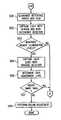
- FIG. 3illustrates an example of a method for capturing and adjusting image data in accordance with the present invention. While sensor station 40 is used to illustrate this aspect of the invention, the method discussed in conjunction with this FIG. 3 may be used with any number of sensor stations and/or views. Image capture engine 34 may also selectively perform the method using some or all of these sensor stations and/or views as desired.
- Steps 300 - 316comprise one embodiment of a method for obtaining and adjusting image data by image capture engine 34 .
- steps 300 - 316are illustrated as separate steps, various steps may be ordered in other logical or functional configurations, or may comprise single steps. It may be helpful to describe generally the method before describing each particular step.
- Image capture engine 34may first optionally determine drift rates for sensor 52 and/or light source 50 , and determine in response to the drift rates whether illumination levels need to be monitored.
- Image capture engine 34may then be optionally initialized with a set of parameters suitable for adjusting data captured from film 60 .
- Image capture engine 34may then obtain initial estimates for sensor, film and illumination parameters.
- Image capture engine 34may monitor illumination levels and adjust signal modulation during the various steps within the method while it is capturing data from film 60 , and/or may adjust image data after the data is captured.
- image capture engine 34may be designed to be operable using sensor 52 and light source 50 whose drift rates may be determined or estimated in optional step 300 . For example, these drift rates may be empirically measured. Image capture engine 34 may utilize these drift rates before or during data capture to determine whether, or how often, to monitor illumination levels so that the dynamic range for image capture engine 34 is closer to the dynamic range for image data to be captured. Such an advantage may improve the signal integrity obtained by image capture engine 34 and thus the signal integrity of each processed image. This determination may be performed in step 300 , or at any suitable place in the method. In the embodiment illustrated in this FIG. 3, this determination is performed in step 310 .
- Image capture engine 34may also dynamically vary the frequency for monitoring the illumination levels as desired. Image capture engine 34 may adjust image data after all data has been captured from film 60 , or after each pixel, column, or two-dimensional region has been captured, as desired. Image capture engine 34 may also control integration time for sensor 52 and/or illumination levels for light source 50 before a region of data is captured. One example of a method for such a priori control is discussed in conjunction with FIG. 4 .
- each sensor station within image capture engine 34may be optionally calibrated with some initial operating characteristics.
- Initializing sensor station 40 in image capture engine 34may reduce variations in optical power over a period of time and/or due to temperature.
- diodes within light source 50 , and/or detectors within sensor 52generally produce thermal transients that follow an impulse upon activation, or turn-on, and decline approximately exponentially over a short period of time. Therefore, it may be desirable to establish a stable operating point or level for light source 50 and sensor 52 to reduce fluctuations in output power and sensitivity.
- Establishing an input operating point for light source 50in turn may stabilize the available signal strength that may be received by sensor 52 , and may reduce the possibility that excess illumination may saturate sensor 52 .
- image capture engine 34may be stabilized by waiting a short period of time, for example, sixty seconds, in order for light source 50 and sensor 52 to reach a nominal operating level. Such levels may be set automatically or manually.
- light source 50may be adjusted to compensate for illumination along a thermal transient output power decay curve while, for example, LED and/or CCD devices warm up.
- an input current to light source 50may be increased/decreased to stabilize its optical output power thereby keeping the image capture engine in a linear operating region.
- Sensor 52may then be used to capture image data from film 60 while its responsivity is in a linear range with respect to light source 50 .
- image capture engine 34initializes sensor 52 and light source 50 .
- image capture engine 34may optionally adjust and/or set sensor and illumination levels for a film type.
- image capture engine 34may adjust and/or set an integration time of sensor 52 and/or an illumination power of light source 50 for an expected density of the film type and expected signal strength. These adjustments may desirably prevent saturation of sensor 52 during capture of image data in image regions within film 60 .
- an initialization set point for such parametersmay be automatically chosen if variation in film types is large.
- Such set pointsmay be stored in, for example, tables, variables, files, or in any other suitable arrangement in RAM 36 a , ROM 36 b , and/or storage medium 38 , or may be manually chosen. On the other hand, if variation between film types is small then some nominal set point may be chosen.
- image capture engine 34may in step 306 use leader 73 to obtain initial estimates of the density of film 60 and determine initial illumination levels. These estimates may be established by obtaining a plurality of readings within a region, such as a column, from leader 73 , or obtaining substantially all data therefrom, whether or not a chemical developer has been applied.
- image capture engine 34begins capturing data from film 60 , by illuminating film 60 using light source 50 and capturing data with sensor 52 . Details for storing and processing captured image data are discussed in conjunction with step 316 .
- image capture engine 34may capture two-dimensional image data from film 60 by utilizing a two-dimensional sensor 52 , such as a staring array.
- a generally linear array sensor 52may obtain a data or image column along the y direction of film 60 as illustrated in FIGS. 2A-2C.
- Film 60may be moved at a scan rate relative to sensor 52 in the x direction as illustrated in FIGS. 2A-2C to obtain a two-dimensional plurality of columns for each latent image in film 60 .
- Image capture engine 34may use an imaging window during which one or more sensors and/or light sources may be used to obtain image data from film 60 .
- the duration of such an imaging windowmay be a length of time sufficient to obtain a desired resolution, such as 12 ⁇ m per square pixel.
- a desired resolutionsuch as 12 ⁇ m per square pixel.
- optics 46 and a generally linear sensor 52may be suitably adjusted to obtain data in the y direction of 12 ⁇ m.
- image capture engine 34may adjust the scan rate to obtain the desired resolution of 12 ⁇ m in the x direction.
- sensor 52may capture a next column of data from film 60 , and repeat this process until all image data from film 60 has been captured.
- a two-dimensional sensor 52may be used to obtain image data for a two-dimensional region from film 60 by using a similar process.
- image capture engine 34determines whether to monitor illumination levels and/or to adjust signal modulation. Where sensor and illumination drift rates are slow relative to the time to capture data from film 60 (total data capture time), image capture engine 34 may determine that no monitoring or adjustment need be performed. Image capture engine 34 may then proceed to step 314 . Alternatively, image capture engine 34 may determine when to perform and/or measure for adjustments as desired, in step 312 . This step may be omitted in some embodiments of the invention, or performed at other stages, such as before each image frame. The invention may include measuring reference and sensed illumination levels, adjusting image data, and/or signal modulation adjustment, after which image capture engine proceeds to step 314 and back to step 308 to capture a next set of image data.
- image capture engine 34may create opportunities to monitor and/or adjust illumination levels.
- Image capture engine 34may also optionally use the captured data to control sensor 52 and/or light source 50 before the next column or region of data is captured by, for example, adjusting illumination power (such as pulse width and/or amplitude) and sensor integration time.
- illumination powersuch as pulse width and/or amplitude
- sensor integration timeOne method for utilizing such an external reference 62 and adjusting signal modulation to achieve desired illumination levels is illustrated and described in further conjunction with FIG. 4 .
- image capture engine 34optionally determines whether all image data from film 60 has been captured. For example, the invention also contemplates on-the-fly image data adjustment, where image capture engine 34 may adjust image data after some or all of the image data has been captured from film 60 . In this example, if all image data has not been captured, image capture engine 34 returns to step 308 to continue the method. If so, image capture engine 34 proceeds to step 316 to adjust the captured image data.
- Image capture engine 34may perform adjustments in step 316 to image data captured using information obtained during steps 304 - 312 .
- Image capture engine 34may determine a gain using data captured by reference detectors to apply to image data captured by sensor 52 . Normalizing the gains of captured image data may also avoid overflow in calculations. Image capture engine 34 then applies these adjustments to the captured image data to reduce the effects of spatial non-uniformities in the captured image data. Because the method may adjust image data captured at a plurality of times, the integrity of the image data may be improved notwithstanding any changes in film density as film 60 develops.
- Image capture engine 34may perform adjustments as frequently as desired as discussed above, on data captured or received by any digital film processing system 10 . Although a plurality of embodiments of an exemplary image capture engine 34 that may be used for image adjustment in connection with the invention have been illustrated, other image capture engines may be used without departing from the scope of the invention.
- Processingmay be performed as desired, including, but not limited to, a pixel, array (such as a data column), or image frame basis. Processing may also be performed in parallel or pipelined. Any or all non-uniformities need not be completely removed during adjustment to fall within the scope of the invention. Accordingly, adjustment includes, but is not limited to, reduction of non-uniformities or errors, or other alterations of pixel data in the captured image. To illustrate this aspect of the invention, adjustment is performed on image data captured in data columns by a generally linear sensor that comprises a plurality of detectors.
- Captured and/ or adjusted image data, as well as data captured from monitoring illumination levels,may be stored as pixel values representing the measured sensor illumination levels. These data may be stored in non-volatile memory such as storage medium 38 for subsequent processing, and/or stored in RAM 36 a , ROM 36 b , or in other storage media within image capture engine 34 for near-simultaneous processing.
- Image capture engine 34may also optionally ensure that image data captured in the x direction is spatially uniform, by using one of many methods to normalize these estimates. For example, image capture engine 34 may determine a new gain factor, or gain level, from the data captured from the unexposed region to achieve the effect of an approximately uniform instantaneous scan across an image frame, and/or the roll of film. This reduces or removes the effects of spatial illumination non-uniformities from subsequent data captured within the image frame.
- This illumination gain factormay be calculated for illumination measurements by a method such as the one described in conjunction with FIG. 4 . Adjustment may be performed here or in step 506 , and on a column-by-column basis.
- Image capture engine 34may then apply this new gain level to each pixel of image data captured from one or more subsequent image frames.
- the new gain levelmay be represented as a gain factor.
- adjustmentmay be performed by, for example, multiplying the gain factor by the captured image data.
- the desired pixel valuemay be a predetermined value, or an averaged value.
- the desired pixel valuemay be an average of a plurality of reference and/or sensing detector values within a plurality of captured data columns in the x-direction.
- image data captured by each sensor stationmay be normalized independently. Such independent processing may be desirable, for example, where image capture engine 34 may utilize different parameters for each sensor station such as light sources using various wavelengths, and/or sensors with varying integration times.
- image capture engine 34may utilize different parameters for each sensor station such as light sources using various wavelengths, and/or sensors with varying integration times.
- each representation of an image captured by a sensor stationmay be recombined and/or undergo other processing to form a single representation of the image.
- FIG. 4illustrates an example of a method for monitoring and adjusting illumination of an image capture system utilizing the teachings of the present invention. While sensor station 40 is used to illustrate this aspect of the invention, the method discussed in conjunction with this FIG. 3 may be used with any number of sensor stations and/or views. Image capture engine 34 may also selectively perform the method using some or all of these sensor stations and/or views as desired. Although steps 500 - 508 are illustrated as separate steps, various steps may be ordered in other logical or functional configurations, or may comprise single steps.
- image capture engine 34uses a reference target 62 or 70 to monitor illumination levels as image data is obtained in the x direction continually or as desired.
- Image capture engine 34may capture reference energy levels from reference detectors and/or sensed energy levels from one or more sensing detectors 61 . Image data may be adjusted in response to these levels as they change between data columns. These adjustments may be desirable, because image capture engine 34 may, for example, maintain a stable input current to light source 50 , the optical output power of light source 50 still typically drifts.
- image capture engine 34may adjust signal modulation by measuring one or more prior pulses of light source 50 and adjusting its signal modulation to a desirable level. This may desirably allow image capture engine 34 to operate independently of content and/or unexposed regions within film 60 , and may also ensure that illumination is generally uniform or varies within a small range.
- step 500the method begins in step 500 , where light source 50 illuminates film 60 and reference target 62 or 70 as illustrated in FIGS. 2A-2C.
- image capture engine 34may utilize sensor 52 to capture data from film 60 , and one or more reference detectors to capture reference energy levels from reference target 62 . Because reflective and transmissive properties of reference target 62 typically do not vary appreciably, image capture engine 34 may use data captured by each reference detector as a reference level. Image capture engine 34 may utilize this reference level to apply gain to subsequent latent image data captured to compensate for slight variations in illumination levels or drifts within the detectors. Such an advantage may minimize the presence of signal noise and may stabilize image capture engine 34 to the extent that detector response variations caused by spectral bandwidth shifts of illumination combined with detector responsivity are relatively constant as a function of wavelength.
- image capture engine 34may average data captured by each plurality of reference detectors to estimate a drift in illumination. Alternatively or in addition, image capture engine 34 may also perform filtering of several prior estimates to correct for illuminator drift and its effects on image data in the x direction, as discussed earlier in conjunction with FIG. 3, at step 316 . For example, image capture engine 34 may use a weighted average from prior data columns.
- image capture engine 34may optionally determine whether to adjust signal modulation in steps 504 - 508 . This may be desirable where signal modulation of light source 50 drifts within a tolerance that may be less than some noise threshold, such as total system noise, or desired noise floor, etc. For example, image capture engine 34 may determine these drifts from initial estimates and/or prior reference and/or sensed energy levels. In some applications, such as where drifts are larger than this tolerance, image capture engine 34 may adjust image data in step 316 as discussed previously. In steps 504 - 508 , image capture engine 34 may optionally adjust light sensor 50 to output relatively uniform illumination levels within some tolerance before image capture engine 34 captures additional data.
- some noise thresholdsuch as total system noise, or desired noise floor, etc.
- image capture engine 34may determine these drifts from initial estimates and/or prior reference and/or sensed energy levels. In some applications, such as where drifts are larger than this tolerance, image capture engine 34 may adjust image data in step 316 as discussed previously.
- image capture engine 34may optionally adjust light sensor 50 to output
- image capture engine 34may capture the current illumination level of a light pulse using sensing detector 61 as a sensed energy level. For example, as a data column is captured, nominal energy levels for detectors within sensor 52 are typically modulated with detector variances. That is, although the energy level values may be the same, detector variances may not be separable from illumination variances. Thus, normalization of both detector variances within sensor 52 as well as illumination variances for light source 50 may be desirable. Image capture engine 34 may utilize and/or create one or more correction factors to correlate energy level values from each sensing detector 61 to those from light source 50 . Image capture engine 34 may then utilize the sensor, camera and/or illumination drift data measured from the sensing detector 61 and/or reference detectors to adjust image data. Alternatively or in addition, image capture engine 34 may adjust sensor integration times, and/or light source amplitude or pulse width levels before the next pulse from light source 50 in response to this data.
- step 506image capture engine 34 calculates the drift in the illumination level of this pulse from a prior light pulse level, and determines an appropriate gain that, if desired in step 507 , may be used to adjust image data in step 316 as discussed previously.
- Image capture engine 34may then apply this new gain level to each pixel of image data captured from one or more subsequent data columns to correct for the drift in illumination.
- the new gainmay be represented as a gain factor.
- adjustmentmay be performed by, for example, multiplying the gain factor by the captured image data or logarithmically subtracting the gain factor from the captured image data.
- the new gain levelmay be calculated by a variety of known methods, using pixel values, illumination levels, or a combination thereof.
- image capture engine 34may measure a desired light level as a pixel value of 2233 (where each pixel comprises twelve (12) bits of resolution).
- the desired pixel valuemay be a predetermined value, or an averaged value.
- the desired pixel valuemay be an average of all prior reference detector values measured in the x-direction.
- the new gain levelmay be obtained by calculating the ratio of the desired value over the measured value. This gain is then multiplied by the actual measurement of each detector to produce a constant referenced value and normalize the entire column to the reference.
- reference detectorsmeasure a lower light level such as 2230
- the new gain valuewill be 2233/2230.
- reference detectors measure a higher light level such as 2235the new gain value will be 2233/2235.
- image capture engine 34may utilize discrete feedback from one or more prior pulses to determine an operating point for a next pulse.
- illumination control 43 , processor 36 , or a combination of the twomay be used to deliver an input signal to light source 50 .
- Image capture engine 34may desirably average measured illumination levels for prior pulses to establish a desired illumination level for the next pulse.
- Image capture engine 34may utilize many types of averaging algorithms or filters, including but not limited to, weighted averages, and infinite or finite impulse response algorithms.
Landscapes
- Engineering & Computer Science (AREA)
- Multimedia (AREA)
- Signal Processing (AREA)
- Facsimile Scanning Arrangements (AREA)
- Investigating Or Analysing Materials By Optical Means (AREA)
Abstract
Description
Claims (10)
Priority Applications (1)
| Application Number | Priority Date | Filing Date | Title |
|---|---|---|---|
| US09/746,859US6788335B2 (en) | 1999-12-30 | 2000-12-21 | Pulsed illumination signal modulation control & adjustment method and system |
Applications Claiming Priority (6)
| Application Number | Priority Date | Filing Date | Title |
|---|---|---|---|
| US17378799P | 1999-12-30 | 1999-12-30 | |
| US17378199P | 1999-12-30 | 1999-12-30 | |
| US17407499P | 1999-12-30 | 1999-12-30 | |
| US17378099P | 1999-12-30 | 1999-12-30 | |
| US17407399P | 1999-12-30 | 1999-12-30 | |
| US09/746,859US6788335B2 (en) | 1999-12-30 | 2000-12-21 | Pulsed illumination signal modulation control & adjustment method and system |
Publications (2)
| Publication Number | Publication Date |
|---|---|
| US20010030686A1 US20010030686A1 (en) | 2001-10-18 |
| US6788335B2true US6788335B2 (en) | 2004-09-07 |
Family
ID=27558628
Family Applications (1)
| Application Number | Title | Priority Date | Filing Date |
|---|---|---|---|
| US09/746,859Expired - Fee RelatedUS6788335B2 (en) | 1999-12-30 | 2000-12-21 | Pulsed illumination signal modulation control & adjustment method and system |
Country Status (1)
| Country | Link |
|---|---|
| US (1) | US6788335B2 (en) |
Cited By (3)
| Publication number | Priority date | Publication date | Assignee | Title |
|---|---|---|---|---|
| US20010052932A1 (en)* | 1999-12-30 | 2001-12-20 | Young Robert S. | Digital film processing method and system |
| US20080002029A1 (en)* | 2006-06-29 | 2008-01-03 | Fan He | Liquid Crystal Testing Apparatus and Method for Image Capture Devices |
| US20090086192A1 (en)* | 2007-09-28 | 2009-04-02 | Fan He | Spectrum Verification Imaging System and Method |
Families Citing this family (3)
| Publication number | Priority date | Publication date | Assignee | Title |
|---|---|---|---|---|
| US10271778B2 (en)* | 2008-06-03 | 2019-04-30 | Nonin Medical, Inc. | LED control utilizing ambient light or signal quality |
| GB201505350D0 (en)* | 2015-03-27 | 2015-05-13 | Imetafilm Ltd | Calibration and validation of motion pictures scans |
| PL3760008T3 (en)* | 2018-02-27 | 2022-01-17 | Signify Holding B.V. | Rendering a dynamic light scene based on one or more light settings |
Citations (154)
| Publication number | Priority date | Publication date | Assignee | Title |
|---|---|---|---|---|
| US2404138A (en) | 1941-10-06 | 1946-07-16 | Alvin L Mayer | Apparatus for developing exposed photographic prints |
| US3520690A (en) | 1965-06-25 | 1970-07-14 | Fuji Photo Film Co Ltd | Process for controlling dye gradation in color photographic element |
| US3520689A (en) | 1965-06-16 | 1970-07-14 | Fuji Photo Film Co Ltd | Color developing process utilizing pyridinium salts |
| US3587435A (en) | 1969-04-24 | 1971-06-28 | Pat P Chioffe | Film processing machine |
| US3615498A (en) | 1967-07-29 | 1971-10-26 | Fuji Photo Film Co Ltd | Color developers containing substituted nbenzyl-p-aminophenol competing developing agents |
| US3615479A (en) | 1968-05-27 | 1971-10-26 | Itek Corp | Automatic film processing method and apparatus therefor |
| US3617282A (en) | 1970-05-18 | 1971-11-02 | Eastman Kodak Co | Nucleating agents for photographic reversal processes |
| US3747120A (en) | 1971-01-11 | 1973-07-17 | N Stemme | Arrangement of writing mechanisms for writing on paper with a coloredliquid |
| US3833161A (en) | 1972-02-08 | 1974-09-03 | Bosch Photokino Gmbh | Apparatus for intercepting and threading the leader of convoluted motion picture film or the like |
| US3903541A (en) | 1971-07-27 | 1975-09-02 | Meister Frederick W Von | Apparatus for processing printing plates precoated on one side only |
| US3946398A (en) | 1970-06-29 | 1976-03-23 | Silonics, Inc. | Method and apparatus for recording with writing fluids and drop projection means therefor |
| US3959048A (en) | 1974-11-29 | 1976-05-25 | Stanfield James S | Apparatus and method for repairing elongated flexible strips having damaged sprocket feed holes along the edge thereof |
| US4026756A (en) | 1976-03-19 | 1977-05-31 | Stanfield James S | Apparatus for repairing elongated flexible strips having damaged sprocket feed holes along the edge thereof |
| US4081577A (en) | 1973-12-26 | 1978-03-28 | American Hoechst Corporation | Pulsed spray of fluids |
| US4142107A (en) | 1977-06-30 | 1979-02-27 | International Business Machines Corporation | Resist development control system |
| US4215927A (en) | 1979-04-13 | 1980-08-05 | Scott Paper Company | Lithographic plate processing apparatus |
| US4249985A (en) | 1979-03-05 | 1981-02-10 | Stanfield James S | Pressure roller for apparatus useful in repairing sprocket holes on strip material |
| US4265545A (en) | 1979-07-27 | 1981-05-05 | Intec Corporation | Multiple source laser scanning inspection system |
| US4301469A (en) | 1980-04-30 | 1981-11-17 | United Technologies Corporation | Run length encoder for color raster scanner |
| US4490729A (en) | 1982-09-15 | 1984-12-25 | The Mead Corporation | Ink jet printer |
| US4501480A (en) | 1981-10-16 | 1985-02-26 | Pioneer Electronic Corporation | System for developing a photo-resist material used as a recording medium |
| US4564280A (en) | 1982-10-28 | 1986-01-14 | Fujitsu Limited | Method and apparatus for developing resist film including a movable nozzle arm |
| US4594598A (en) | 1982-10-26 | 1986-06-10 | Sharp Kabushiki Kaisha | Printer head mounting assembly in an ink jet system printer |
| US4621037A (en) | 1984-07-09 | 1986-11-04 | Sigma Corporation | Method for detecting endpoint of development |
| US4623236A (en) | 1985-10-31 | 1986-11-18 | Polaroid Corporation | Photographic processing composition applicator |
| US4633300A (en) | 1983-10-21 | 1986-12-30 | Canon Kabushiki Kaisha | Color information detecting device |
| US4636808A (en) | 1985-09-09 | 1987-01-13 | Eastman Kodak Company | Continuous ink jet printer |
| US4666307A (en) | 1984-01-19 | 1987-05-19 | Fuji Photo Film Co., Ltd. | Method for calibrating photographic image information |
| US4670779A (en) | 1984-01-10 | 1987-06-02 | Sharp Kabushiki Kaisha | Color-picture analyzing apparatus with red-purpose and green-purpose filters |
| US4688099A (en)* | 1985-06-07 | 1987-08-18 | Eastman Kodak Company | Illumination control circuitry for a film video player electronic strobe light |
| EP0261782A2 (en) | 1986-08-15 | 1988-03-30 | Konica Corporation | A color image processing apparatus |
| US4736221A (en) | 1985-10-18 | 1988-04-05 | Fuji Photo Film Co., Ltd. | Method and device for processing photographic film using atomized liquid processing agents |
| US4741621A (en) | 1986-08-18 | 1988-05-03 | Westinghouse Electric Corp. | Geometric surface inspection system with dual overlap light stripe generator |
| US4745040A (en) | 1976-08-27 | 1988-05-17 | Levine Alfred B | Method for destructive electronic development of photo film |
| US4755844A (en) | 1985-04-30 | 1988-07-05 | Kabushiki Kaisha Toshiba | Automatic developing device |
| US4777102A (en) | 1976-08-27 | 1988-10-11 | Levine Alfred B | Method and apparatus for electronic development of color photographic film |
| US4796061A (en) | 1985-11-16 | 1989-01-03 | Dainippon Screen Mfg. Co., Ltd. | Device for detachably attaching a film onto a drum in a drum type picture scanning recording apparatus |
| US4814630A (en) | 1987-06-29 | 1989-03-21 | Ncr Corporation | Document illuminating apparatus using light sources A, B, and C in periodic arrays |
| US4821114A (en) | 1986-05-02 | 1989-04-11 | Dr. Ing. Rudolf Hell Gmbh | Opto-electronic scanning arrangement |
| US4845551A (en) | 1985-05-31 | 1989-07-04 | Fuji Photo Film Co., Ltd. | Method for correcting color photographic image data on the basis of calibration data read from a reference film |
| US4851311A (en) | 1987-12-17 | 1989-07-25 | Texas Instruments Incorporated | Process for determining photoresist develop time by optical transmission |
| US4857430A (en) | 1987-12-17 | 1989-08-15 | Texas Instruments Incorporated | Process and system for determining photoresist development endpoint by effluent analysis |
| US4875067A (en) | 1987-07-23 | 1989-10-17 | Fuji Photo Film Co., Ltd. | Processing apparatus |
| US4969045A (en) | 1988-05-20 | 1990-11-06 | Sanyo Electric Co., Ltd. | Image sensing apparatus having automatic iris function of automatically adjusting exposure in response to video signal |
| US4994918A (en) | 1989-04-28 | 1991-02-19 | Bts Broadcast Television Systems Gmbh | Method and circuit for the automatic correction of errors in image steadiness during film scanning |
| EP0422220A1 (en) | 1989-03-28 | 1991-04-17 | Yokogawa Medical Systems, Ltd | Image processing apparatus |
| US5027146A (en) | 1989-08-31 | 1991-06-25 | Eastman Kodak Company | Processing apparatus |
| US5034767A (en) | 1987-08-28 | 1991-07-23 | Hanetz International Inc. | Development system |
| US5101286A (en) | 1990-03-21 | 1992-03-31 | Eastman Kodak Company | Scanning film during the film process for output to a video monitor |
| US5124216A (en) | 1990-07-31 | 1992-06-23 | At&T Bell Laboratories | Method for monitoring photoresist latent images |
| US5155596A (en) | 1990-12-03 | 1992-10-13 | Eastman Kodak Company | Film scanner illumination system having an automatic light control |
| US5196285A (en) | 1990-05-18 | 1993-03-23 | Xinix, Inc. | Method for control of photoresist develop processes |
| US5200817A (en) | 1991-08-29 | 1993-04-06 | Xerox Corporation | Conversion of an RGB color scanner into a colorimetric scanner |
| EP0525886A3 (en) | 1991-07-25 | 1993-05-12 | Eastman Kodak Company | Coater for low flowrate coating |
| US5212512A (en) | 1990-11-30 | 1993-05-18 | Fuji Photo Film Co., Ltd. | Photofinishing system |
| US5231439A (en) | 1990-08-03 | 1993-07-27 | Fuji Photo Film Co., Ltd. | Photographic film handling method |
| US5235352A (en) | 1991-08-16 | 1993-08-10 | Compaq Computer Corporation | High density ink jet printhead |
| US5255408A (en) | 1992-02-11 | 1993-10-26 | Eastman Kodak Company | Photographic film cleaner |
| US5267030A (en) | 1989-12-22 | 1993-11-30 | Eastman Kodak Company | Method and associated apparatus for forming image data metrics which achieve media compatibility for subsequent imaging application |
| US5266805A (en) | 1992-05-05 | 1993-11-30 | International Business Machines Corporation | System and method for image recovery |
| EP0580293A1 (en) | 1992-07-17 | 1994-01-26 | International Business Machines Corporation | Scanning film during the film process |
| US5296923A (en) | 1991-01-09 | 1994-03-22 | Konica Corporation | Color image reproducing device and method |
| EP0601364A1 (en) | 1992-11-30 | 1994-06-15 | Konica Corporation | Film image editing apparatus |
| US5350651A (en) | 1993-02-12 | 1994-09-27 | Eastman Kodak Company | Methods for the retrieval and differentiation of blue, green and red exposure records of the same hue from photographic elements containing absorbing interlayers |
| US5350664A (en) | 1993-02-12 | 1994-09-27 | Eastman Kodak Company | Photographic elements for producing blue, green, and red exposure records of the same hue and methods for the retrieval and differentiation of the exposure records |
| US5357307A (en) | 1992-11-25 | 1994-10-18 | Eastman Kodak Company | Apparatus for processing photosensitive material |
| US5360701A (en) | 1991-01-05 | 1994-11-01 | Ilford Limited | Antistatic backing for photographic roll film |
| US5371542A (en) | 1992-06-23 | 1994-12-06 | The United States Of America As Represented By The Secretary Of The Navy | Dual waveband signal processing system |
| US5391443A (en) | 1991-07-19 | 1995-02-21 | Eastman Kodak Company | Process for the extraction of spectral image records from dye image forming photographic elements |
| US5414779A (en) | 1993-06-14 | 1995-05-09 | Eastman Kodak Company | Image frame detection |
| US5416550A (en) | 1990-09-14 | 1995-05-16 | Eastman Kodak Company | Photographic processing apparatus |
| US5418597A (en) | 1992-09-14 | 1995-05-23 | Eastman Kodak Company | Clamping arrangement for film scanning apparatus |
| US5418119A (en) | 1993-07-16 | 1995-05-23 | Eastman Kodak Company | Photographic elements for producing blue, green and red exposure records of the same hue |
| US5432579A (en) | 1991-10-03 | 1995-07-11 | Fuji Photo Film Co., Ltd. | Photograph printing system |
| US5436738A (en) | 1992-01-22 | 1995-07-25 | Eastman Kodak Company | Three dimensional thermal internegative photographic printing apparatus and method |
| US5440365A (en) | 1993-10-14 | 1995-08-08 | Eastman Kodak Company | Photosensitive material processor |
| EP0669753A2 (en) | 1994-02-28 | 1995-08-30 | Minolta Co., Ltd. | An apparatus for reproducing images |
| US5447811A (en) | 1992-09-24 | 1995-09-05 | Eastman Kodak Company | Color image reproduction of scenes with preferential tone mapping |
| US5448380A (en) | 1993-07-31 | 1995-09-05 | Samsung Electronics Co., Ltd. | color image processing method and apparatus for correcting a color signal from an input image device |
| US5452018A (en) | 1991-04-19 | 1995-09-19 | Sony Electronics Inc. | Digital color correction system having gross and fine adjustment modes |
| US5465155A (en) | 1992-07-17 | 1995-11-07 | International Business Machines Corporation | Duplex film scanning |
| US5477345A (en) | 1993-12-15 | 1995-12-19 | Xerox Corporation | Apparatus for subsampling chrominance |
| EP0482790B1 (en) | 1990-10-23 | 1996-01-03 | Crosfield Electronics Limited | Method and apparatus for generating representation of an image |
| US5496669A (en) | 1992-07-01 | 1996-03-05 | Interuniversitair Micro-Elektronica Centrum Vzw | System for detecting a latent image using an alignment apparatus |
| US5516608A (en) | 1994-02-28 | 1996-05-14 | International Business Machines Corporation | Method for controlling a line dimension arising in photolithographic processes |
| US5519510A (en) | 1992-07-17 | 1996-05-21 | International Business Machines Corporation | Electronic film development |
| US5528288A (en)* | 1993-06-08 | 1996-06-18 | Eastman Kodak Company | Illumination control system for a film scanner |
| US5546477A (en) | 1993-03-30 | 1996-08-13 | Klics, Inc. | Data compression and decompression |
| US5550566A (en) | 1993-07-15 | 1996-08-27 | Media Vision, Inc. | Video capture expansion card |
| US5552904A (en) | 1994-01-31 | 1996-09-03 | Samsung Electronics Co., Ltd. | Color correction method and apparatus using adaptive region separation |
| US5563717A (en) | 1995-02-03 | 1996-10-08 | Eastman Kodak Company | Method and means for calibration of photographic media using pre-exposed miniature images |
| US5568270A (en) | 1992-12-09 | 1996-10-22 | Fuji Photo Film Co., Ltd. | Image reading apparatus which varies reading time according to image density |
| US5576836A (en) | 1993-10-29 | 1996-11-19 | Minolta Co., Ltd. | Multi-picture image printing system |
| US5581376A (en) | 1994-08-29 | 1996-12-03 | Xerox Corporation | System for correcting color images using tetrahedral interpolation over a hexagonal lattice |
| US5587752A (en) | 1995-06-05 | 1996-12-24 | Eastman Kodak Company | Camera, system and method for producing composite photographic image |
| US5596415A (en) | 1993-06-14 | 1997-01-21 | Eastman Kodak Company | Iterative predictor-based detection of image frame locations |
| EP0768571A2 (en) | 1995-09-18 | 1997-04-16 | Noritsu Koki Co., Ltd. | Film connecting device |
| US5627016A (en) | 1996-02-29 | 1997-05-06 | Eastman Kodak Company | Method and apparatus for photofinishing photosensitive film |
| US5649260A (en) | 1995-06-26 | 1997-07-15 | Eastman Kodak Company | Automated photofinishing apparatus |
| US5664255A (en) | 1996-05-29 | 1997-09-02 | Eastman Kodak Company | Photographic printing and processing apparatus |
| US5664253A (en) | 1995-09-12 | 1997-09-02 | Eastman Kodak Company | Stand alone photofinishing apparatus |
| EP0794454A2 (en) | 1996-03-04 | 1997-09-10 | Fuji Photo Film Co., Ltd. | Film scanner |
| US5667944A (en) | 1995-10-25 | 1997-09-16 | Eastman Kodak Company | Digital process sensitivity correction |
| US5678116A (en) | 1994-04-06 | 1997-10-14 | Dainippon Screen Mfg. Co., Ltd. | Method and apparatus for drying a substrate having a resist film with a miniaturized pattern |
| EP0806861A1 (en) | 1996-05-10 | 1997-11-12 | Noritsu Koki Co., Ltd. | Electronic image printing apparatus attachable to a photographic processing apparatus |
| US5691118A (en) | 1996-10-10 | 1997-11-25 | Eastman Kodak Company | Color paper processing using two acidic stop solutions before and after bleaching |
| US5695914A (en) | 1995-09-15 | 1997-12-09 | Eastman Kodak Company | Process of forming a dye image |
| US5698382A (en) | 1995-09-25 | 1997-12-16 | Konica Corporation | Processing method for silver halide color photographic light-sensitive material |
| US5726773A (en) | 1994-11-29 | 1998-03-10 | Carl-Zeiss-Stiftung | Apparatus for scanning and digitizing photographic image objects and method of operating said apparatus |
| US5739897A (en) | 1994-08-16 | 1998-04-14 | Gretag Imaging Ag | Method and system for creating index prints on and/or with a photographic printer |
| WO1998025399A1 (en) | 1996-12-05 | 1998-06-11 | Applied Science Fiction, Inc. | Method and apparatus for reducing noise in electronic film development |
| US5771107A (en) | 1995-01-11 | 1998-06-23 | Mita Industrial Co., Ltd. | Image processor with image edge emphasizing capability |
| US5784529A (en)* | 1994-10-18 | 1998-07-21 | Rank Cintel Limited | Method and apparatus for correcting noise in a film scanner |
| US5790277A (en) | 1994-06-08 | 1998-08-04 | International Business Machines Corporation | Duplex film scanning |
| WO1998034157A2 (en) | 1997-01-30 | 1998-08-06 | Applied Science Fiction, Inc. | System and method for latent film recovery in electronic film development |
| US5835795A (en) | 1996-06-25 | 1998-11-10 | Photo Dimensions | Blended photographic composite images |
| US5835811A (en) | 1995-08-31 | 1998-11-10 | Noritsu Koki Co., Ltd. | Photosensitive material processing apparatus |
| EP0878777A2 (en) | 1997-05-09 | 1998-11-18 | Xerox Corporation | Method for enhancement of reduced color set images |
| US5870172A (en) | 1996-03-29 | 1999-02-09 | Blume; Stephen T. | Apparatus for producing a video and digital image directly from dental x-ray film |
| US5880819A (en) | 1995-06-29 | 1999-03-09 | Fuji Photo Film Co., Ltd. | Photographic film loading method, photographic film conveying apparatus, and image reading apparatus |
| US5892595A (en) | 1996-01-26 | 1999-04-06 | Ricoh Company, Ltd. | Image reading apparatus for correct positioning of color component values of each picture element |
| EP0930498A2 (en) | 1997-12-26 | 1999-07-21 | Nidek Co., Ltd. | Inspection apparatus and method for detecting defects |
| US5930388A (en) | 1996-10-24 | 1999-07-27 | Sharp Kabuskiki Kaisha | Color image processing apparatus |
| WO1999043149A1 (en) | 1998-02-23 | 1999-08-26 | Applied Science Fiction, Inc. | Progressive area scan in electronic film development |
| US5959720A (en) | 1996-03-22 | 1999-09-28 | Eastman Kodak Company | Method for color balance determination |
| US5963662A (en) | 1996-08-07 | 1999-10-05 | Georgia Tech Research Corporation | Inspection system and method for bond detection and validation of surface mount devices |
| US5966465A (en) | 1994-09-21 | 1999-10-12 | Ricoh Corporation | Compression/decompression using reversible embedded wavelets |
| US5982936A (en) | 1995-04-18 | 1999-11-09 | Advanced Micro Devices, Inc. | Performance of video decompression by using block oriented data structures |
| US5982937A (en) | 1996-12-24 | 1999-11-09 | Electronics For Imaging, Inc. | Apparatus and method for hybrid compression of raster data |
| US5982951A (en) | 1996-05-28 | 1999-11-09 | Canon Kabushiki Kaisha | Apparatus and method for combining a plurality of images |
| US5979011A (en) | 1995-04-07 | 1999-11-09 | Noritsu Koki Co., Ltd | Dust removing apparatus |
| US5982941A (en) | 1997-02-07 | 1999-11-09 | Eastman Kodak Company | Method of producing digital image with improved performance characteristic |
| US5982427A (en)* | 1995-02-10 | 1999-11-09 | Innovation Tk Ltd. | Digital image processing |
| US5991444A (en) | 1994-11-14 | 1999-11-23 | Sarnoff Corporation | Method and apparatus for performing mosaic based image compression |
| US5988896A (en) | 1996-10-26 | 1999-11-23 | Applied Science Fiction, Inc. | Method and apparatus for electronic film development |
| US5998109A (en) | 1997-12-24 | 1999-12-07 | Konica Corporation | Method for a silver halide light-sensitive photographic material and development reading method |
| US6000284A (en) | 1997-04-02 | 1999-12-14 | Board Of Trustees Operating Michigan State University | Method and apparatus for determining and quantifying resistance to scuff damage of a film adhered on a panel |
| US6005987A (en) | 1996-10-17 | 1999-12-21 | Sharp Kabushiki Kaisha | Picture image forming apparatus |
| US6034719A (en)* | 1996-04-19 | 2000-03-07 | Nikon Corporation | Image input apparatus |
| US6065824A (en) | 1994-12-22 | 2000-05-23 | Hewlett-Packard Company | Method and apparatus for storing information on a replaceable ink container |
| US6088084A (en) | 1997-10-17 | 2000-07-11 | Fuji Photo Film Co., Ltd. | Original carrier and image reader |
| US6089687A (en) | 1998-03-09 | 2000-07-18 | Hewlett-Packard Company | Method and apparatus for specifying ink volume in an ink container |
| US6101273A (en) | 1995-10-31 | 2000-08-08 | Fuji Photo Film Co., Ltd. | Image reproducing method and apparatus |
| US6102508A (en) | 1996-09-27 | 2000-08-15 | Hewlett-Packard Company | Method and apparatus for selecting printer consumables |
| US6137965A (en) | 1998-12-22 | 2000-10-24 | Gid Gmbh | Container for developing equipment |
| WO2001013174A1 (en) | 1999-08-17 | 2001-02-22 | Applied Science Fiction, Inc. | Method and system for using calibration patches in electronic film processing |
| US6200738B1 (en) | 1998-10-29 | 2001-03-13 | Konica Corporation | Image forming method |
| WO2001045042A1 (en) | 1999-12-17 | 2001-06-21 | Applied Science Fiction, Inc. | Method and system for selective enhancement of image data |
| WO2001050197A1 (en) | 1999-12-30 | 2001-07-12 | Applied Science Fiction, Inc. | System and method for digital color dye film processing |
| WO2001050194A1 (en) | 1999-12-30 | 2001-07-12 | Applied Science Fiction, Inc. | System and method for digital film development using visible light |
| WO2001050193A1 (en) | 1999-12-30 | 2001-07-12 | Applied Science Fiction, Inc. | Improved system and method for digital film development using visible light |
| WO2001050192A1 (en) | 1999-12-31 | 2001-07-12 | Applied Science Fiction, Inc. | Digital film processing method |
| WO2001052556A2 (en) | 1999-12-30 | 2001-07-19 | Applied Science Fiction, Inc. | Methods and apparatus for transporting and positioning film in a digital film processing system |
| US6542179B1 (en)* | 1998-09-30 | 2003-04-01 | Eastman Kodak Company | Light integrating system with reduced dynamic shading |
- 2000
- 2000-12-21USUS09/746,859patent/US6788335B2/ennot_activeExpired - Fee Related
Patent Citations (157)
| Publication number | Priority date | Publication date | Assignee | Title |
|---|---|---|---|---|
| US2404138A (en) | 1941-10-06 | 1946-07-16 | Alvin L Mayer | Apparatus for developing exposed photographic prints |
| US3520689A (en) | 1965-06-16 | 1970-07-14 | Fuji Photo Film Co Ltd | Color developing process utilizing pyridinium salts |
| US3520690A (en) | 1965-06-25 | 1970-07-14 | Fuji Photo Film Co Ltd | Process for controlling dye gradation in color photographic element |
| US3615498A (en) | 1967-07-29 | 1971-10-26 | Fuji Photo Film Co Ltd | Color developers containing substituted nbenzyl-p-aminophenol competing developing agents |
| US3615479A (en) | 1968-05-27 | 1971-10-26 | Itek Corp | Automatic film processing method and apparatus therefor |
| US3587435A (en) | 1969-04-24 | 1971-06-28 | Pat P Chioffe | Film processing machine |
| US3617282A (en) | 1970-05-18 | 1971-11-02 | Eastman Kodak Co | Nucleating agents for photographic reversal processes |
| US3946398A (en) | 1970-06-29 | 1976-03-23 | Silonics, Inc. | Method and apparatus for recording with writing fluids and drop projection means therefor |
| US3747120A (en) | 1971-01-11 | 1973-07-17 | N Stemme | Arrangement of writing mechanisms for writing on paper with a coloredliquid |
| US3903541A (en) | 1971-07-27 | 1975-09-02 | Meister Frederick W Von | Apparatus for processing printing plates precoated on one side only |
| US3833161A (en) | 1972-02-08 | 1974-09-03 | Bosch Photokino Gmbh | Apparatus for intercepting and threading the leader of convoluted motion picture film or the like |
| US4081577A (en) | 1973-12-26 | 1978-03-28 | American Hoechst Corporation | Pulsed spray of fluids |
| US3959048A (en) | 1974-11-29 | 1976-05-25 | Stanfield James S | Apparatus and method for repairing elongated flexible strips having damaged sprocket feed holes along the edge thereof |
| US4026756A (en) | 1976-03-19 | 1977-05-31 | Stanfield James S | Apparatus for repairing elongated flexible strips having damaged sprocket feed holes along the edge thereof |
| US4745040A (en) | 1976-08-27 | 1988-05-17 | Levine Alfred B | Method for destructive electronic development of photo film |
| US4777102A (en) | 1976-08-27 | 1988-10-11 | Levine Alfred B | Method and apparatus for electronic development of color photographic film |
| US4142107A (en) | 1977-06-30 | 1979-02-27 | International Business Machines Corporation | Resist development control system |
| US4249985A (en) | 1979-03-05 | 1981-02-10 | Stanfield James S | Pressure roller for apparatus useful in repairing sprocket holes on strip material |
| US4215927A (en) | 1979-04-13 | 1980-08-05 | Scott Paper Company | Lithographic plate processing apparatus |
| US4265545A (en) | 1979-07-27 | 1981-05-05 | Intec Corporation | Multiple source laser scanning inspection system |
| US4301469A (en) | 1980-04-30 | 1981-11-17 | United Technologies Corporation | Run length encoder for color raster scanner |
| US4501480A (en) | 1981-10-16 | 1985-02-26 | Pioneer Electronic Corporation | System for developing a photo-resist material used as a recording medium |
| US4490729A (en) | 1982-09-15 | 1984-12-25 | The Mead Corporation | Ink jet printer |
| US4594598A (en) | 1982-10-26 | 1986-06-10 | Sharp Kabushiki Kaisha | Printer head mounting assembly in an ink jet system printer |
| US4564280A (en) | 1982-10-28 | 1986-01-14 | Fujitsu Limited | Method and apparatus for developing resist film including a movable nozzle arm |
| US4633300A (en) | 1983-10-21 | 1986-12-30 | Canon Kabushiki Kaisha | Color information detecting device |
| US4670779A (en) | 1984-01-10 | 1987-06-02 | Sharp Kabushiki Kaisha | Color-picture analyzing apparatus with red-purpose and green-purpose filters |
| US4666307A (en) | 1984-01-19 | 1987-05-19 | Fuji Photo Film Co., Ltd. | Method for calibrating photographic image information |
| US4621037A (en) | 1984-07-09 | 1986-11-04 | Sigma Corporation | Method for detecting endpoint of development |
| US4755844A (en) | 1985-04-30 | 1988-07-05 | Kabushiki Kaisha Toshiba | Automatic developing device |
| US4845551A (en) | 1985-05-31 | 1989-07-04 | Fuji Photo Film Co., Ltd. | Method for correcting color photographic image data on the basis of calibration data read from a reference film |
| US4688099A (en)* | 1985-06-07 | 1987-08-18 | Eastman Kodak Company | Illumination control circuitry for a film video player electronic strobe light |
| US4636808A (en) | 1985-09-09 | 1987-01-13 | Eastman Kodak Company | Continuous ink jet printer |
| US4736221A (en) | 1985-10-18 | 1988-04-05 | Fuji Photo Film Co., Ltd. | Method and device for processing photographic film using atomized liquid processing agents |
| US4623236A (en) | 1985-10-31 | 1986-11-18 | Polaroid Corporation | Photographic processing composition applicator |
| US4796061A (en) | 1985-11-16 | 1989-01-03 | Dainippon Screen Mfg. Co., Ltd. | Device for detachably attaching a film onto a drum in a drum type picture scanning recording apparatus |
| US4821114A (en) | 1986-05-02 | 1989-04-11 | Dr. Ing. Rudolf Hell Gmbh | Opto-electronic scanning arrangement |
| EP0261782A2 (en) | 1986-08-15 | 1988-03-30 | Konica Corporation | A color image processing apparatus |
| US4741621A (en) | 1986-08-18 | 1988-05-03 | Westinghouse Electric Corp. | Geometric surface inspection system with dual overlap light stripe generator |
| US4814630A (en) | 1987-06-29 | 1989-03-21 | Ncr Corporation | Document illuminating apparatus using light sources A, B, and C in periodic arrays |
| US4875067A (en) | 1987-07-23 | 1989-10-17 | Fuji Photo Film Co., Ltd. | Processing apparatus |
| US5034767A (en) | 1987-08-28 | 1991-07-23 | Hanetz International Inc. | Development system |
| US4851311A (en) | 1987-12-17 | 1989-07-25 | Texas Instruments Incorporated | Process for determining photoresist develop time by optical transmission |
| US4857430A (en) | 1987-12-17 | 1989-08-15 | Texas Instruments Incorporated | Process and system for determining photoresist development endpoint by effluent analysis |
| US4969045A (en) | 1988-05-20 | 1990-11-06 | Sanyo Electric Co., Ltd. | Image sensing apparatus having automatic iris function of automatically adjusting exposure in response to video signal |
| EP0422220A1 (en) | 1989-03-28 | 1991-04-17 | Yokogawa Medical Systems, Ltd | Image processing apparatus |
| US4994918A (en) | 1989-04-28 | 1991-02-19 | Bts Broadcast Television Systems Gmbh | Method and circuit for the automatic correction of errors in image steadiness during film scanning |
| US5027146A (en) | 1989-08-31 | 1991-06-25 | Eastman Kodak Company | Processing apparatus |
| US5267030A (en) | 1989-12-22 | 1993-11-30 | Eastman Kodak Company | Method and associated apparatus for forming image data metrics which achieve media compatibility for subsequent imaging application |
| US5101286A (en) | 1990-03-21 | 1992-03-31 | Eastman Kodak Company | Scanning film during the film process for output to a video monitor |
| US5292605A (en) | 1990-05-18 | 1994-03-08 | Xinix, Inc. | Method for control of photoresist develop processes |
| US5196285A (en) | 1990-05-18 | 1993-03-23 | Xinix, Inc. | Method for control of photoresist develop processes |
| US5124216A (en) | 1990-07-31 | 1992-06-23 | At&T Bell Laboratories | Method for monitoring photoresist latent images |
| US5231439A (en) | 1990-08-03 | 1993-07-27 | Fuji Photo Film Co., Ltd. | Photographic film handling method |
| US5416550A (en) | 1990-09-14 | 1995-05-16 | Eastman Kodak Company | Photographic processing apparatus |
| EP0482790B1 (en) | 1990-10-23 | 1996-01-03 | Crosfield Electronics Limited | Method and apparatus for generating representation of an image |
| US5212512A (en) | 1990-11-30 | 1993-05-18 | Fuji Photo Film Co., Ltd. | Photofinishing system |
| US5155596A (en) | 1990-12-03 | 1992-10-13 | Eastman Kodak Company | Film scanner illumination system having an automatic light control |
| US5360701A (en) | 1991-01-05 | 1994-11-01 | Ilford Limited | Antistatic backing for photographic roll film |
| US5296923A (en) | 1991-01-09 | 1994-03-22 | Konica Corporation | Color image reproducing device and method |
| US5452018A (en) | 1991-04-19 | 1995-09-19 | Sony Electronics Inc. | Digital color correction system having gross and fine adjustment modes |
| US5391443A (en) | 1991-07-19 | 1995-02-21 | Eastman Kodak Company | Process for the extraction of spectral image records from dye image forming photographic elements |
| US5334247A (en) | 1991-07-25 | 1994-08-02 | Eastman Kodak Company | Coater design for low flowrate coating applications |
| EP0525886A3 (en) | 1991-07-25 | 1993-05-12 | Eastman Kodak Company | Coater for low flowrate coating |
| US5235352A (en) | 1991-08-16 | 1993-08-10 | Compaq Computer Corporation | High density ink jet printhead |
| US5200817A (en) | 1991-08-29 | 1993-04-06 | Xerox Corporation | Conversion of an RGB color scanner into a colorimetric scanner |
| US5432579A (en) | 1991-10-03 | 1995-07-11 | Fuji Photo Film Co., Ltd. | Photograph printing system |
| US5436738A (en) | 1992-01-22 | 1995-07-25 | Eastman Kodak Company | Three dimensional thermal internegative photographic printing apparatus and method |
| US5255408A (en) | 1992-02-11 | 1993-10-26 | Eastman Kodak Company | Photographic film cleaner |
| US5266805A (en) | 1992-05-05 | 1993-11-30 | International Business Machines Corporation | System and method for image recovery |
| US5371542A (en) | 1992-06-23 | 1994-12-06 | The United States Of America As Represented By The Secretary Of The Navy | Dual waveband signal processing system |
| US5496669A (en) | 1992-07-01 | 1996-03-05 | Interuniversitair Micro-Elektronica Centrum Vzw | System for detecting a latent image using an alignment apparatus |
| US5519510A (en) | 1992-07-17 | 1996-05-21 | International Business Machines Corporation | Electronic film development |
| US5465155A (en) | 1992-07-17 | 1995-11-07 | International Business Machines Corporation | Duplex film scanning |
| EP0580293A1 (en) | 1992-07-17 | 1994-01-26 | International Business Machines Corporation | Scanning film during the film process |
| US5418597A (en) | 1992-09-14 | 1995-05-23 | Eastman Kodak Company | Clamping arrangement for film scanning apparatus |
| US5447811A (en) | 1992-09-24 | 1995-09-05 | Eastman Kodak Company | Color image reproduction of scenes with preferential tone mapping |
| US5357307A (en) | 1992-11-25 | 1994-10-18 | Eastman Kodak Company | Apparatus for processing photosensitive material |
| EP0601364A1 (en) | 1992-11-30 | 1994-06-15 | Konica Corporation | Film image editing apparatus |
| US5568270A (en) | 1992-12-09 | 1996-10-22 | Fuji Photo Film Co., Ltd. | Image reading apparatus which varies reading time according to image density |
| US5350651A (en) | 1993-02-12 | 1994-09-27 | Eastman Kodak Company | Methods for the retrieval and differentiation of blue, green and red exposure records of the same hue from photographic elements containing absorbing interlayers |
| US5350664A (en) | 1993-02-12 | 1994-09-27 | Eastman Kodak Company | Photographic elements for producing blue, green, and red exposure records of the same hue and methods for the retrieval and differentiation of the exposure records |
| US5546477A (en) | 1993-03-30 | 1996-08-13 | Klics, Inc. | Data compression and decompression |
| US5528288A (en)* | 1993-06-08 | 1996-06-18 | Eastman Kodak Company | Illumination control system for a film scanner |
| US5596415A (en) | 1993-06-14 | 1997-01-21 | Eastman Kodak Company | Iterative predictor-based detection of image frame locations |
| US5414779A (en) | 1993-06-14 | 1995-05-09 | Eastman Kodak Company | Image frame detection |
| US5550566A (en) | 1993-07-15 | 1996-08-27 | Media Vision, Inc. | Video capture expansion card |
| US5418119A (en) | 1993-07-16 | 1995-05-23 | Eastman Kodak Company | Photographic elements for producing blue, green and red exposure records of the same hue |
| US5448380A (en) | 1993-07-31 | 1995-09-05 | Samsung Electronics Co., Ltd. | color image processing method and apparatus for correcting a color signal from an input image device |
| US5440365A (en) | 1993-10-14 | 1995-08-08 | Eastman Kodak Company | Photosensitive material processor |
| US5576836A (en) | 1993-10-29 | 1996-11-19 | Minolta Co., Ltd. | Multi-picture image printing system |
| US5477345A (en) | 1993-12-15 | 1995-12-19 | Xerox Corporation | Apparatus for subsampling chrominance |
| US5552904A (en) | 1994-01-31 | 1996-09-03 | Samsung Electronics Co., Ltd. | Color correction method and apparatus using adaptive region separation |
| EP0669753A2 (en) | 1994-02-28 | 1995-08-30 | Minolta Co., Ltd. | An apparatus for reproducing images |
| US5516608A (en) | 1994-02-28 | 1996-05-14 | International Business Machines Corporation | Method for controlling a line dimension arising in photolithographic processes |
| US5678116A (en) | 1994-04-06 | 1997-10-14 | Dainippon Screen Mfg. Co., Ltd. | Method and apparatus for drying a substrate having a resist film with a miniaturized pattern |
| US5790277A (en) | 1994-06-08 | 1998-08-04 | International Business Machines Corporation | Duplex film scanning |
| US5739897A (en) | 1994-08-16 | 1998-04-14 | Gretag Imaging Ag | Method and system for creating index prints on and/or with a photographic printer |
| US5581376A (en) | 1994-08-29 | 1996-12-03 | Xerox Corporation | System for correcting color images using tetrahedral interpolation over a hexagonal lattice |
| US5966465A (en) | 1994-09-21 | 1999-10-12 | Ricoh Corporation | Compression/decompression using reversible embedded wavelets |
| US5784529A (en)* | 1994-10-18 | 1998-07-21 | Rank Cintel Limited | Method and apparatus for correcting noise in a film scanner |
| US5991444A (en) | 1994-11-14 | 1999-11-23 | Sarnoff Corporation | Method and apparatus for performing mosaic based image compression |
| US5726773A (en) | 1994-11-29 | 1998-03-10 | Carl-Zeiss-Stiftung | Apparatus for scanning and digitizing photographic image objects and method of operating said apparatus |
| US6065824A (en) | 1994-12-22 | 2000-05-23 | Hewlett-Packard Company | Method and apparatus for storing information on a replaceable ink container |
| US5771107A (en) | 1995-01-11 | 1998-06-23 | Mita Industrial Co., Ltd. | Image processor with image edge emphasizing capability |
| US5563717A (en) | 1995-02-03 | 1996-10-08 | Eastman Kodak Company | Method and means for calibration of photographic media using pre-exposed miniature images |
| US5982427A (en)* | 1995-02-10 | 1999-11-09 | Innovation Tk Ltd. | Digital image processing |
| US5979011A (en) | 1995-04-07 | 1999-11-09 | Noritsu Koki Co., Ltd | Dust removing apparatus |
| US5982936A (en) | 1995-04-18 | 1999-11-09 | Advanced Micro Devices, Inc. | Performance of video decompression by using block oriented data structures |
| US5587752A (en) | 1995-06-05 | 1996-12-24 | Eastman Kodak Company | Camera, system and method for producing composite photographic image |
| US5649260A (en) | 1995-06-26 | 1997-07-15 | Eastman Kodak Company | Automated photofinishing apparatus |
| US5880819A (en) | 1995-06-29 | 1999-03-09 | Fuji Photo Film Co., Ltd. | Photographic film loading method, photographic film conveying apparatus, and image reading apparatus |
| US5835811A (en) | 1995-08-31 | 1998-11-10 | Noritsu Koki Co., Ltd. | Photosensitive material processing apparatus |
| US5664253A (en) | 1995-09-12 | 1997-09-02 | Eastman Kodak Company | Stand alone photofinishing apparatus |
| US5695914A (en) | 1995-09-15 | 1997-12-09 | Eastman Kodak Company | Process of forming a dye image |
| EP0768571A2 (en) | 1995-09-18 | 1997-04-16 | Noritsu Koki Co., Ltd. | Film connecting device |
| US5698382A (en) | 1995-09-25 | 1997-12-16 | Konica Corporation | Processing method for silver halide color photographic light-sensitive material |
| US5667944A (en) | 1995-10-25 | 1997-09-16 | Eastman Kodak Company | Digital process sensitivity correction |
| US6101273A (en) | 1995-10-31 | 2000-08-08 | Fuji Photo Film Co., Ltd. | Image reproducing method and apparatus |
| US5892595A (en) | 1996-01-26 | 1999-04-06 | Ricoh Company, Ltd. | Image reading apparatus for correct positioning of color component values of each picture element |
| US5627016A (en) | 1996-02-29 | 1997-05-06 | Eastman Kodak Company | Method and apparatus for photofinishing photosensitive film |
| EP0794454A2 (en) | 1996-03-04 | 1997-09-10 | Fuji Photo Film Co., Ltd. | Film scanner |
| US5959720A (en) | 1996-03-22 | 1999-09-28 | Eastman Kodak Company | Method for color balance determination |
| US5870172A (en) | 1996-03-29 | 1999-02-09 | Blume; Stephen T. | Apparatus for producing a video and digital image directly from dental x-ray film |
| US6034719A (en)* | 1996-04-19 | 2000-03-07 | Nikon Corporation | Image input apparatus |
| EP0806861A1 (en) | 1996-05-10 | 1997-11-12 | Noritsu Koki Co., Ltd. | Electronic image printing apparatus attachable to a photographic processing apparatus |
| US5982951A (en) | 1996-05-28 | 1999-11-09 | Canon Kabushiki Kaisha | Apparatus and method for combining a plurality of images |
| US5664255A (en) | 1996-05-29 | 1997-09-02 | Eastman Kodak Company | Photographic printing and processing apparatus |
| US5835795A (en) | 1996-06-25 | 1998-11-10 | Photo Dimensions | Blended photographic composite images |
| US5963662A (en) | 1996-08-07 | 1999-10-05 | Georgia Tech Research Corporation | Inspection system and method for bond detection and validation of surface mount devices |
| US6102508A (en) | 1996-09-27 | 2000-08-15 | Hewlett-Packard Company | Method and apparatus for selecting printer consumables |
| US5691118A (en) | 1996-10-10 | 1997-11-25 | Eastman Kodak Company | Color paper processing using two acidic stop solutions before and after bleaching |
| US6005987A (en) | 1996-10-17 | 1999-12-21 | Sharp Kabushiki Kaisha | Picture image forming apparatus |
| US5930388A (en) | 1996-10-24 | 1999-07-27 | Sharp Kabuskiki Kaisha | Color image processing apparatus |
| US5988896A (en) | 1996-10-26 | 1999-11-23 | Applied Science Fiction, Inc. | Method and apparatus for electronic film development |
| US6069714A (en) | 1996-12-05 | 2000-05-30 | Applied Science Fiction, Inc. | Method and apparatus for reducing noise in electronic film development |
| WO1998025399A1 (en) | 1996-12-05 | 1998-06-11 | Applied Science Fiction, Inc. | Method and apparatus for reducing noise in electronic film development |
| US5982937A (en) | 1996-12-24 | 1999-11-09 | Electronics For Imaging, Inc. | Apparatus and method for hybrid compression of raster data |
| WO1998034157A2 (en) | 1997-01-30 | 1998-08-06 | Applied Science Fiction, Inc. | System and method for latent film recovery in electronic film development |
| US5982941A (en) | 1997-02-07 | 1999-11-09 | Eastman Kodak Company | Method of producing digital image with improved performance characteristic |
| US6000284A (en) | 1997-04-02 | 1999-12-14 | Board Of Trustees Operating Michigan State University | Method and apparatus for determining and quantifying resistance to scuff damage of a film adhered on a panel |
| EP0878777A2 (en) | 1997-05-09 | 1998-11-18 | Xerox Corporation | Method for enhancement of reduced color set images |
| US6088084A (en) | 1997-10-17 | 2000-07-11 | Fuji Photo Film Co., Ltd. | Original carrier and image reader |
| US5998109A (en) | 1997-12-24 | 1999-12-07 | Konica Corporation | Method for a silver halide light-sensitive photographic material and development reading method |
| EP0930498A2 (en) | 1997-12-26 | 1999-07-21 | Nidek Co., Ltd. | Inspection apparatus and method for detecting defects |
| WO1999043149A1 (en) | 1998-02-23 | 1999-08-26 | Applied Science Fiction, Inc. | Progressive area scan in electronic film development |
| US6089687A (en) | 1998-03-09 | 2000-07-18 | Hewlett-Packard Company | Method and apparatus for specifying ink volume in an ink container |
| US6542179B1 (en)* | 1998-09-30 | 2003-04-01 | Eastman Kodak Company | Light integrating system with reduced dynamic shading |
| US6200738B1 (en) | 1998-10-29 | 2001-03-13 | Konica Corporation | Image forming method |
| US6137965A (en) | 1998-12-22 | 2000-10-24 | Gid Gmbh | Container for developing equipment |
| WO2001013174A1 (en) | 1999-08-17 | 2001-02-22 | Applied Science Fiction, Inc. | Method and system for using calibration patches in electronic film processing |
| WO2001045042A1 (en) | 1999-12-17 | 2001-06-21 | Applied Science Fiction, Inc. | Method and system for selective enhancement of image data |
| WO2001050197A1 (en) | 1999-12-30 | 2001-07-12 | Applied Science Fiction, Inc. | System and method for digital color dye film processing |
| WO2001050194A1 (en) | 1999-12-30 | 2001-07-12 | Applied Science Fiction, Inc. | System and method for digital film development using visible light |
| WO2001050193A1 (en) | 1999-12-30 | 2001-07-12 | Applied Science Fiction, Inc. | Improved system and method for digital film development using visible light |
| WO2001052556A2 (en) | 1999-12-30 | 2001-07-19 | Applied Science Fiction, Inc. | Methods and apparatus for transporting and positioning film in a digital film processing system |
| WO2001050192A1 (en) | 1999-12-31 | 2001-07-12 | Applied Science Fiction, Inc. | Digital film processing method |
Non-Patent Citations (11)
| Title |
|---|
| "A Method of Characteristics Model of a Drop-on-Demand Ink-Jet Device Using an Integral Method Drop Formation Model", D. Wallace, MicroFab Technologies, Inc., The American Society of Mechanical Engineers, Winter Annual Meeting, pp. 1-9, Dec. 10-15, 1989. |
| "Adaptive Fourier Threshold Filtering: A Method to Reduce Noise and Incoherent Artifacts in High Resolution Cardiac Images", Doyle, M., et al., 8306 Magnetic Resonance in Medicine 31, No. 5, Baltimore, MD, May, 1994, pp. 546-550. |
| "Adaptive-neighborhood filtering of images corrupted by signal-dependent noise", R. Rangayyan, et al., Applied Optics, vol. 37, No. 20, pp. 4477-4487, Jul. 10, 1998. |
| "Anisotropic Spectral Magnitude Estimation Filters for Noise Reduction and Image Enhancement", T. Aach, et al., Philips GmbH Research Laboratories, IEEE, pp. 335-338, 1996. |
| "Digital Imaging Equipment White Papers", Putting Damaged Film on ICE, www.nikonusa.com/reference/whitepapers/imaging, Nikon Corporation, Nov. 28, 2000. |
| "Grayscale Characteristics", The Nature of Color Images, Photographic Negatives, pp. 163-168. |
| "Ink-Jet Based Fluid Microdispensing in Biochemical Applications", D. Wallace, MicroFab Technologies, Inc., Laboratory Automation News, vol. 1, No. 5, pp. 3, 6-9, Nov., 1996. |
| "Low-Cost Display Assembly and Interconnect Using Ink-Jet Printing Technology", D. Hayes, et al., Display Works '99, MicroFab Technologies, Inc., pp. 1-4, 1999. |
| "MicroJet Printing of Solder and Polymers for Multi-Chip Modules and Chip-Scale Package", D. Hayes, et al., MicroFab Technologies, Inc. (6 pages). |
| "Parallel Production of Oligonucleotide Arrays Using Membranes and Reagent Jet Printing", D. Stimpson, et al., Research Reports, BioTechniques, vol. 25, No. 5, pp. 886-890, 1998. |
| "Photorealistic Ink-Jet Printing Through Dynamic Spot Size Control", D. Wallace, et al., Journal of Imaging Science and Technology, vol. 40, No. 5, pp. 390-395, Sep./Oct. 1996. |
Cited By (5)
| Publication number | Priority date | Publication date | Assignee | Title |
|---|---|---|---|---|
| US20010052932A1 (en)* | 1999-12-30 | 2001-12-20 | Young Robert S. | Digital film processing method and system |
| US20080002029A1 (en)* | 2006-06-29 | 2008-01-03 | Fan He | Liquid Crystal Testing Apparatus and Method for Image Capture Devices |
| US7764322B2 (en)* | 2006-06-29 | 2010-07-27 | Motorola, Inc. | Liquid crystal testing apparatus and method for image capture devices |
| US20090086192A1 (en)* | 2007-09-28 | 2009-04-02 | Fan He | Spectrum Verification Imaging System and Method |
| US7773224B2 (en) | 2007-09-28 | 2010-08-10 | Motorola, Inc. | Spectrum verification imaging system and method |
Also Published As
| Publication number | Publication date |
|---|---|
| US20010030686A1 (en) | 2001-10-18 |
Similar Documents
| Publication | Publication Date | Title |
|---|---|---|
| US6707557B2 (en) | Method and system for estimating sensor dark current drift and sensor/illumination non-uniformities | |
| JP4478358B2 (en) | Digital image processing method and apparatus for brightness adjustment of digital image | |
| US6751349B2 (en) | Image processing system | |
| US7489396B1 (en) | Spectrophotometric camera | |
| EP1455523B1 (en) | Scanning device calibration system and method | |
| BE1008076A3 (en) | COLOR NEGATIVE SCANNING AND TRANSFORMATION IN COLORS OF ORIGINAL scene. | |
| JP2011030261A (en) | Apparatus and method for high dynamic range imaging using spatially varying exposures | |
| US7433097B2 (en) | Optical image scanner with moveable calibration target | |
| EP2710340B1 (en) | Camera arrangement for a vehicle and method for calibrating a camera and for operating a camera arrangement | |
| US20230392986A1 (en) | Nonlinearity correction and range fitting for stereoscopy through illumination and approaches to using the same for noncontact color determination | |
| US6788335B2 (en) | Pulsed illumination signal modulation control & adjustment method and system | |
| US7599559B2 (en) | Method for collecting data for color measurements from a digital electronic image capturing device or system | |
| US20020140996A1 (en) | Optical image scanner using pre-scan and post-scan compensation for illumination nonuniformity | |
| US20020100863A1 (en) | Optical image scanner with color and intensity compensation during lamp warmup | |
| US20010033702A1 (en) | Method and apparatus for aligning multiple scans of the same area of a medium using mathematical correlation | |
| US6816604B2 (en) | Digital film processing feature location method and system | |
| US20010052932A1 (en) | Digital film processing method and system | |
| CN100543572C (en) | Imaging system, imaging device analysis system, imaging device analysis method, and beam emitting method | |
| US7268925B1 (en) | Image sensor optimization | |
| Mizoguchi | Evaluation of image sensors | |
| JPH1188898A (en) | Image reader | |
| CN105590941A (en) | Method for improving photoelectric sensor and light-sensitive material weak light detection ability | |
| US7773805B2 (en) | Method and apparatus for flare cancellation for image contrast restoration | |
| US20010048766A1 (en) | Time invariant feature location method and system | |
| CA2330433A1 (en) | Smart exposure determination for imagers |
Legal Events
| Date | Code | Title | Description |
|---|---|---|---|
| AS | Assignment | Owner name:APPLIED SCIENCE FICTION, INC., TEXAS Free format text:ASSIGNMENT OF ASSIGNORS INTEREST;ASSIGNORS:YOUNG, ROBERT S. JR.;DIGBY, MARC C.;HANSEN, CHRISTOPHER P.;AND OTHERS;REEL/FRAME:011707/0959;SIGNING DATES FROM 20010404 TO 20010409 | |
| AS | Assignment | Owner name:CENTERPOINT VENTURE PARTNERS, L.P., TEXAS Free format text:SECURITY AGREEMENT;ASSIGNOR:APPLIED SCIENCE FICTION, INC.;REEL/FRAME:012997/0211 Effective date:20020723 Owner name:CENTERPOINT VENTURE PARTNERS, L.P., TEXAS Free format text:SECURITY INTEREST;ASSIGNOR:APPLIED SCIENCE FICTION, INC.;REEL/FRAME:012997/0113 Effective date:20020723 Owner name:RHO VENTURES (QP), L.P., NEW YORK Free format text:SECURITY AGREEMENT;ASSIGNOR:APPLIED SCIENCE FICTION, INC.;REEL/FRAME:012997/0211 Effective date:20020723 Owner name:RHO VENTURES (QP), L.P., NEW YORK Free format text:SECURITY INTEREST;ASSIGNOR:APPLIED SCIENCE FICTION, INC.;REEL/FRAME:012997/0113 Effective date:20020723 | |
| AS | Assignment | Owner name:CENTERPOINT VENTURE PARTNERS, L.P., TEXAS Free format text:SECURITY AGREEMENT;ASSIGNOR:APPLIED SCIENCE FICTION, INC.;REEL/FRAME:013506/0065 Effective date:20030213 Owner name:RHO VENTURES (QP), L.P., NEW YORK Free format text:SECURITY AGREEMENT;ASSIGNOR:APPLIED SCIENCE FICTION, INC.;REEL/FRAME:013506/0065 Effective date:20030213 | |
| AS | Assignment | Owner name:EASTMAN KODAK COMPANY, NEW YORK Free format text:ASSIGNMENT OF ASSIGNORS INTEREST;ASSIGNOR:APPLIED SCIENCE FICTION, INC.;REEL/FRAME:014293/0774 Effective date:20030521 | |
| FEPP | Fee payment procedure | Free format text:PAYOR NUMBER ASSIGNED (ORIGINAL EVENT CODE: ASPN); ENTITY STATUS OF PATENT OWNER: LARGE ENTITY | |
| FPAY | Fee payment | Year of fee payment:4 | |
| AS | Assignment | Owner name:APPLIED SCIENCE FICTION, INC., TEXAS Free format text:RELEASE BY SECURED PARTY;ASSIGNORS:CENTERPOINT VENTURE PARTNERS, L.P.;RHO VENTURES (QP), L.P.;REEL/FRAME:027294/0740 Effective date:20030521 Owner name:EASTMAN KODAK COMPANY, NEW YORK Free format text:RELEASE BY SECURED PARTY;ASSIGNORS:CENTERPOINT VENTURE PARTNERS, L.P.;RHO VENTURES (QP), L.P.;REEL/FRAME:027294/0740 Effective date:20030521 | |
| AS | Assignment | Owner name:CITICORP NORTH AMERICA, INC., AS AGENT, NEW YORK Free format text:SECURITY INTEREST;ASSIGNORS:EASTMAN KODAK COMPANY;PAKON, INC.;REEL/FRAME:028201/0420 Effective date:20120215 | |
| FPAY | Fee payment | Year of fee payment:8 | |
| AS | Assignment | Owner name:WILMINGTON TRUST, NATIONAL ASSOCIATION, AS AGENT, Free format text:PATENT SECURITY AGREEMENT;ASSIGNORS:EASTMAN KODAK COMPANY;PAKON, INC.;REEL/FRAME:030122/0235 Effective date:20130322 Owner name:WILMINGTON TRUST, NATIONAL ASSOCIATION, AS AGENT, MINNESOTA Free format text:PATENT SECURITY AGREEMENT;ASSIGNORS:EASTMAN KODAK COMPANY;PAKON, INC.;REEL/FRAME:030122/0235 Effective date:20130322 | |
| AS | Assignment | Owner name:BANK OF AMERICA N.A., AS AGENT, MASSACHUSETTS Free format text:INTELLECTUAL PROPERTY SECURITY AGREEMENT (ABL);ASSIGNORS:EASTMAN KODAK COMPANY;FAR EAST DEVELOPMENT LTD.;FPC INC.;AND OTHERS;REEL/FRAME:031162/0117 Effective date:20130903 Owner name:BARCLAYS BANK PLC, AS ADMINISTRATIVE AGENT, NEW YORK Free format text:INTELLECTUAL PROPERTY SECURITY AGREEMENT (SECOND LIEN);ASSIGNORS:EASTMAN KODAK COMPANY;FAR EAST DEVELOPMENT LTD.;FPC INC.;AND OTHERS;REEL/FRAME:031159/0001 Effective date:20130903 Owner name:JPMORGAN CHASE BANK, N.A., AS ADMINISTRATIVE, DELAWARE Free format text:INTELLECTUAL PROPERTY SECURITY AGREEMENT (FIRST LIEN);ASSIGNORS:EASTMAN KODAK COMPANY;FAR EAST DEVELOPMENT LTD.;FPC INC.;AND OTHERS;REEL/FRAME:031158/0001 Effective date:20130903 Owner name:BARCLAYS BANK PLC, AS ADMINISTRATIVE AGENT, NEW YO Free format text:INTELLECTUAL PROPERTY SECURITY AGREEMENT (SECOND LIEN);ASSIGNORS:EASTMAN KODAK COMPANY;FAR EAST DEVELOPMENT LTD.;FPC INC.;AND OTHERS;REEL/FRAME:031159/0001 Effective date:20130903 Owner name:EASTMAN KODAK COMPANY, NEW YORK Free format text:RELEASE OF SECURITY INTEREST IN PATENTS;ASSIGNORS:CITICORP NORTH AMERICA, INC., AS SENIOR DIP AGENT;WILMINGTON TRUST, NATIONAL ASSOCIATION, AS JUNIOR DIP AGENT;REEL/FRAME:031157/0451 Effective date:20130903 Owner name:PAKON, INC., NEW YORK Free format text:RELEASE OF SECURITY INTEREST IN PATENTS;ASSIGNORS:CITICORP NORTH AMERICA, INC., AS SENIOR DIP AGENT;WILMINGTON TRUST, NATIONAL ASSOCIATION, AS JUNIOR DIP AGENT;REEL/FRAME:031157/0451 Effective date:20130903 Owner name:JPMORGAN CHASE BANK, N.A., AS ADMINISTRATIVE, DELA Free format text:INTELLECTUAL PROPERTY SECURITY AGREEMENT (FIRST LIEN);ASSIGNORS:EASTMAN KODAK COMPANY;FAR EAST DEVELOPMENT LTD.;FPC INC.;AND OTHERS;REEL/FRAME:031158/0001 Effective date:20130903 | |
| REMI | Maintenance fee reminder mailed | ||
| LAPS | Lapse for failure to pay maintenance fees | ||
| STCH | Information on status: patent discontinuation | Free format text:PATENT EXPIRED DUE TO NONPAYMENT OF MAINTENANCE FEES UNDER 37 CFR 1.362 | |
| FP | Lapsed due to failure to pay maintenance fee | Effective date:20160907 | |
| AS | Assignment | Owner name:LASER PACIFIC MEDIA CORPORATION, NEW YORK Free format text:RELEASE BY SECURED PARTY;ASSIGNOR:JP MORGAN CHASE BANK, N.A., AS ADMINISTRATIVE AGENT;REEL/FRAME:049814/0001 Effective date:20190617 Owner name:CREO MANUFACTURING AMERICA LLC, NEW YORK Free format text:RELEASE BY SECURED PARTY;ASSIGNOR:JP MORGAN CHASE BANK, N.A., AS ADMINISTRATIVE AGENT;REEL/FRAME:049814/0001 Effective date:20190617 Owner name:PAKON, INC., NEW YORK Free format text:RELEASE BY SECURED PARTY;ASSIGNOR:JP MORGAN CHASE BANK, N.A., AS ADMINISTRATIVE AGENT;REEL/FRAME:049814/0001 Effective date:20190617 Owner name:KODAK AVIATION LEASING LLC, NEW YORK Free format text:RELEASE BY SECURED PARTY;ASSIGNOR:JP MORGAN CHASE BANK, N.A., AS ADMINISTRATIVE AGENT;REEL/FRAME:049814/0001 Effective date:20190617 Owner name:KODAK (NEAR EAST), INC., NEW YORK Free format text:RELEASE BY SECURED PARTY;ASSIGNOR:JP MORGAN CHASE BANK, N.A., AS ADMINISTRATIVE AGENT;REEL/FRAME:049814/0001 Effective date:20190617 Owner name:FPC, INC., NEW YORK Free format text:RELEASE BY SECURED PARTY;ASSIGNOR:JP MORGAN CHASE BANK, N.A., AS ADMINISTRATIVE AGENT;REEL/FRAME:049814/0001 Effective date:20190617 Owner name:KODAK REALTY, INC., NEW YORK Free format text:RELEASE BY SECURED PARTY;ASSIGNOR:JP MORGAN CHASE BANK, N.A., AS ADMINISTRATIVE AGENT;REEL/FRAME:049814/0001 Effective date:20190617 Owner name:KODAK PHILIPPINES, LTD., NEW YORK Free format text:RELEASE BY SECURED PARTY;ASSIGNOR:JP MORGAN CHASE BANK, N.A., AS ADMINISTRATIVE AGENT;REEL/FRAME:049814/0001 Effective date:20190617 Owner name:KODAK PORTUGUESA LIMITED, NEW YORK Free format text:RELEASE BY SECURED PARTY;ASSIGNOR:JP MORGAN CHASE BANK, N.A., AS ADMINISTRATIVE AGENT;REEL/FRAME:049814/0001 Effective date:20190617 Owner name:KODAK AMERICAS, LTD., NEW YORK Free format text:RELEASE BY SECURED PARTY;ASSIGNOR:JP MORGAN CHASE BANK, N.A., AS ADMINISTRATIVE AGENT;REEL/FRAME:049814/0001 Effective date:20190617 Owner name:QUALEX, INC., NEW YORK Free format text:RELEASE BY SECURED PARTY;ASSIGNOR:JP MORGAN CHASE BANK, N.A., AS ADMINISTRATIVE AGENT;REEL/FRAME:049814/0001 Effective date:20190617 Owner name:NPEC, INC., NEW YORK Free format text:RELEASE BY SECURED PARTY;ASSIGNOR:JP MORGAN CHASE BANK, N.A., AS ADMINISTRATIVE AGENT;REEL/FRAME:049814/0001 Effective date:20190617 Owner name:EASTMAN KODAK COMPANY, NEW YORK Free format text:RELEASE BY SECURED PARTY;ASSIGNOR:JP MORGAN CHASE BANK, N.A., AS ADMINISTRATIVE AGENT;REEL/FRAME:049814/0001 Effective date:20190617 Owner name:FAR EAST DEVELOPMENT LTD., NEW YORK Free format text:RELEASE BY SECURED PARTY;ASSIGNOR:JP MORGAN CHASE BANK, N.A., AS ADMINISTRATIVE AGENT;REEL/FRAME:049814/0001 Effective date:20190617 Owner name:KODAK IMAGING NETWORK, INC., NEW YORK Free format text:RELEASE BY SECURED PARTY;ASSIGNOR:JP MORGAN CHASE BANK, N.A., AS ADMINISTRATIVE AGENT;REEL/FRAME:049814/0001 Effective date:20190617 | |
| AS | Assignment | Owner name:FPC INC., NEW YORK Free format text:RELEASE BY SECURED PARTY;ASSIGNOR:BARCLAYS BANK PLC;REEL/FRAME:052773/0001 Effective date:20170202 Owner name:EASTMAN KODAK COMPANY, NEW YORK Free format text:RELEASE BY SECURED PARTY;ASSIGNOR:BARCLAYS BANK PLC;REEL/FRAME:052773/0001 Effective date:20170202 Owner name:KODAK PHILIPPINES LTD., NEW YORK Free format text:RELEASE BY SECURED PARTY;ASSIGNOR:BARCLAYS BANK PLC;REEL/FRAME:052773/0001 Effective date:20170202 Owner name:KODAK (NEAR EAST) INC., NEW YORK Free format text:RELEASE BY SECURED PARTY;ASSIGNOR:BARCLAYS BANK PLC;REEL/FRAME:052773/0001 Effective date:20170202 Owner name:LASER PACIFIC MEDIA CORPORATION, NEW YORK Free format text:RELEASE BY SECURED PARTY;ASSIGNOR:BARCLAYS BANK PLC;REEL/FRAME:052773/0001 Effective date:20170202 Owner name:KODAK AMERICAS LTD., NEW YORK Free format text:RELEASE BY SECURED PARTY;ASSIGNOR:BARCLAYS BANK PLC;REEL/FRAME:052773/0001 Effective date:20170202 Owner name:NPEC INC., NEW YORK Free format text:RELEASE BY SECURED PARTY;ASSIGNOR:BARCLAYS BANK PLC;REEL/FRAME:052773/0001 Effective date:20170202 Owner name:FAR EAST DEVELOPMENT LTD., NEW YORK Free format text:RELEASE BY SECURED PARTY;ASSIGNOR:BARCLAYS BANK PLC;REEL/FRAME:052773/0001 Effective date:20170202 Owner name:QUALEX INC., NEW YORK Free format text:RELEASE BY SECURED PARTY;ASSIGNOR:BARCLAYS BANK PLC;REEL/FRAME:052773/0001 Effective date:20170202 Owner name:KODAK REALTY INC., NEW YORK Free format text:RELEASE BY SECURED PARTY;ASSIGNOR:BARCLAYS BANK PLC;REEL/FRAME:052773/0001 Effective date:20170202 |