US6787915B2 - Rearrangement sheet, semiconductor device and method of manufacturing thereof - Google Patents
Rearrangement sheet, semiconductor device and method of manufacturing thereofDownload PDFInfo
- Publication number
- US6787915B2 US6787915B2US09/930,710US93071001AUS6787915B2US 6787915 B2US6787915 B2US 6787915B2US 93071001 AUS93071001 AUS 93071001AUS 6787915 B2US6787915 B2US 6787915B2
- Authority
- US
- United States
- Prior art keywords
- rearrangement
- sheet
- patterns
- conductive metallic
- conductive
- Prior art date
- Legal status (The legal status is an assumption and is not a legal conclusion. Google has not performed a legal analysis and makes no representation as to the accuracy of the status listed.)
- Expired - Fee Related
Links
- 230000008707rearrangementEffects0.000titleclaimsabstractdescription156
- 239000004065semiconductorSubstances0.000titleclaimsabstractdescription95
- 238000004519manufacturing processMethods0.000titleabstractdescription35
- 239000002184metalSubstances0.000claimsdescription43
- 229910052751metalInorganic materials0.000claimsdescription43
- 230000001070adhesive effectEffects0.000claimsdescription38
- 239000000853adhesiveSubstances0.000claimsdescription37
- 239000000758substrateSubstances0.000claimsdescription22
- 230000015572biosynthetic processEffects0.000claimsdescription6
- 230000008878couplingEffects0.000claims1
- 238000010168coupling processMethods0.000claims1
- 238000005859coupling reactionMethods0.000claims1
- 238000010276constructionMethods0.000abstractdescription17
- 238000007789sealingMethods0.000description18
- 239000010931goldSubstances0.000description13
- 239000010949copperSubstances0.000description12
- 238000010586diagramMethods0.000description11
- 238000000034methodMethods0.000description11
- 239000000463materialSubstances0.000description10
- 239000011347resinSubstances0.000description10
- 229920005989resinPolymers0.000description10
- 229910052802copperInorganic materials0.000description5
- 239000003822epoxy resinSubstances0.000description5
- 238000000227grindingMethods0.000description5
- 229920000647polyepoxidePolymers0.000description5
- 229910000679solderInorganic materials0.000description5
- RYGMFSIKBFXOCR-UHFFFAOYSA-NCopperChemical compound[Cu]RYGMFSIKBFXOCR-UHFFFAOYSA-N0.000description4
- 239000002313adhesive filmSubstances0.000description4
- 238000009713electroplatingMethods0.000description4
- 230000007246mechanismEffects0.000description4
- 238000007747platingMethods0.000description4
- 238000001723curingMethods0.000description3
- 230000000694effectsEffects0.000description3
- 238000010438heat treatmentMethods0.000description3
- 238000003475laminationMethods0.000description3
- PXHVJJICTQNCMI-UHFFFAOYSA-NnickelSubstances[Ni]PXHVJJICTQNCMI-UHFFFAOYSA-N0.000description3
- KDLHZDBZIXYQEI-UHFFFAOYSA-NpalladiumSubstances[Pd]KDLHZDBZIXYQEI-UHFFFAOYSA-N0.000description3
- 230000008569processEffects0.000description3
- 239000002131composite materialSubstances0.000description2
- 238000010030laminatingMethods0.000description2
- 239000004850liquid epoxy resins (LERs)Substances0.000description2
- 229920006122polyamide resinPolymers0.000description2
- 229920001721polyimidePolymers0.000description2
- 230000009467reductionEffects0.000description2
- 239000004642PolyimideSubstances0.000description1
- 230000006978adaptationEffects0.000description1
- 238000002507cathodic stripping potentiometryMethods0.000description1
- 239000000470constituentSubstances0.000description1
- 150000001879copperChemical class0.000description1
- 230000007547defectEffects0.000description1
- 238000005530etchingMethods0.000description1
- PCHJSUWPFVWCPO-UHFFFAOYSA-NgoldChemical compound[Au]PCHJSUWPFVWCPO-UHFFFAOYSA-N0.000description1
- 229910052737goldInorganic materials0.000description1
- 230000012447hatchingEffects0.000description1
- 238000013007heat curingMethods0.000description1
- 239000007788liquidSubstances0.000description1
- 229910052759nickelInorganic materials0.000description1
- 229910000510noble metalInorganic materials0.000description1
- 229910052763palladiumInorganic materials0.000description1
- 239000009719polyimide resinSubstances0.000description1
- 230000004044responseEffects0.000description1
- 238000004904shorteningMethods0.000description1
- 238000009751slip formingMethods0.000description1
Images


Classifications
- H—ELECTRICITY
- H01—ELECTRIC ELEMENTS
- H01L—SEMICONDUCTOR DEVICES NOT COVERED BY CLASS H10
- H01L24/00—Arrangements for connecting or disconnecting semiconductor or solid-state bodies; Methods or apparatus related thereto
- H01L24/01—Means for bonding being attached to, or being formed on, the surface to be connected, e.g. chip-to-package, die-attach, "first-level" interconnects; Manufacturing methods related thereto
- H01L24/26—Layer connectors, e.g. plate connectors, solder or adhesive layers; Manufacturing methods related thereto
- H01L24/31—Structure, shape, material or disposition of the layer connectors after the connecting process
- H01L24/32—Structure, shape, material or disposition of the layer connectors after the connecting process of an individual layer connector
- H—ELECTRICITY
- H01—ELECTRIC ELEMENTS
- H01L—SEMICONDUCTOR DEVICES NOT COVERED BY CLASS H10
- H01L23/00—Details of semiconductor or other solid state devices
- H01L23/28—Encapsulations, e.g. encapsulating layers, coatings, e.g. for protection
- H01L23/31—Encapsulations, e.g. encapsulating layers, coatings, e.g. for protection characterised by the arrangement or shape
- H01L23/3107—Encapsulations, e.g. encapsulating layers, coatings, e.g. for protection characterised by the arrangement or shape the device being completely enclosed
- H01L23/3121—Encapsulations, e.g. encapsulating layers, coatings, e.g. for protection characterised by the arrangement or shape the device being completely enclosed a substrate forming part of the encapsulation
- H—ELECTRICITY
- H01—ELECTRIC ELEMENTS
- H01L—SEMICONDUCTOR DEVICES NOT COVERED BY CLASS H10
- H01L23/00—Details of semiconductor or other solid state devices
- H01L23/48—Arrangements for conducting electric current to or from the solid state body in operation, e.g. leads, terminal arrangements ; Selection of materials therefor
- H01L23/488—Arrangements for conducting electric current to or from the solid state body in operation, e.g. leads, terminal arrangements ; Selection of materials therefor consisting of soldered or bonded constructions
- H01L23/498—Leads, i.e. metallisations or lead-frames on insulating substrates, e.g. chip carriers
- H01L23/49838—Geometry or layout
- H—ELECTRICITY
- H01—ELECTRIC ELEMENTS
- H01L—SEMICONDUCTOR DEVICES NOT COVERED BY CLASS H10
- H01L24/00—Arrangements for connecting or disconnecting semiconductor or solid-state bodies; Methods or apparatus related thereto
- H01L24/01—Means for bonding being attached to, or being formed on, the surface to be connected, e.g. chip-to-package, die-attach, "first-level" interconnects; Manufacturing methods related thereto
- H01L24/42—Wire connectors; Manufacturing methods related thereto
- H01L24/47—Structure, shape, material or disposition of the wire connectors after the connecting process
- H01L24/49—Structure, shape, material or disposition of the wire connectors after the connecting process of a plurality of wire connectors
- H—ELECTRICITY
- H01—ELECTRIC ELEMENTS
- H01L—SEMICONDUCTOR DEVICES NOT COVERED BY CLASS H10
- H01L2221/00—Processes or apparatus adapted for the manufacture or treatment of semiconductor or solid state devices or of parts thereof covered by H01L21/00
- H01L2221/67—Apparatus for handling semiconductor or electric solid state devices during manufacture or treatment thereof; Apparatus for handling wafers during manufacture or treatment of semiconductor or electric solid state devices or components; Apparatus not specifically provided for elsewhere
- H01L2221/683—Apparatus for handling semiconductor or electric solid state devices during manufacture or treatment thereof; Apparatus for handling wafers during manufacture or treatment of semiconductor or electric solid state devices or components; Apparatus not specifically provided for elsewhere for supporting or gripping
- H01L2221/68304—Apparatus for handling semiconductor or electric solid state devices during manufacture or treatment thereof; Apparatus for handling wafers during manufacture or treatment of semiconductor or electric solid state devices or components; Apparatus not specifically provided for elsewhere for supporting or gripping using temporarily an auxiliary support
- H01L2221/68318—Auxiliary support including means facilitating the separation of a device or wafer from the auxiliary support
- H01L2221/68322—Auxiliary support including means facilitating the selective separation of some of a plurality of devices from the auxiliary support
- H—ELECTRICITY
- H01—ELECTRIC ELEMENTS
- H01L—SEMICONDUCTOR DEVICES NOT COVERED BY CLASS H10
- H01L2224/00—Indexing scheme for arrangements for connecting or disconnecting semiconductor or solid-state bodies and methods related thereto as covered by H01L24/00
- H01L2224/01—Means for bonding being attached to, or being formed on, the surface to be connected, e.g. chip-to-package, die-attach, "first-level" interconnects; Manufacturing methods related thereto
- H01L2224/02—Bonding areas; Manufacturing methods related thereto
- H01L2224/023—Redistribution layers [RDL] for bonding areas
- H—ELECTRICITY
- H01—ELECTRIC ELEMENTS
- H01L—SEMICONDUCTOR DEVICES NOT COVERED BY CLASS H10
- H01L2224/00—Indexing scheme for arrangements for connecting or disconnecting semiconductor or solid-state bodies and methods related thereto as covered by H01L24/00
- H01L2224/01—Means for bonding being attached to, or being formed on, the surface to be connected, e.g. chip-to-package, die-attach, "first-level" interconnects; Manufacturing methods related thereto
- H01L2224/02—Bonding areas; Manufacturing methods related thereto
- H01L2224/04—Structure, shape, material or disposition of the bonding areas prior to the connecting process
- H01L2224/05—Structure, shape, material or disposition of the bonding areas prior to the connecting process of an individual bonding area
- H01L2224/0554—External layer
- H01L2224/0555—Shape
- H01L2224/05552—Shape in top view
- H01L2224/05554—Shape in top view being square
- H—ELECTRICITY
- H01—ELECTRIC ELEMENTS
- H01L—SEMICONDUCTOR DEVICES NOT COVERED BY CLASS H10
- H01L2224/00—Indexing scheme for arrangements for connecting or disconnecting semiconductor or solid-state bodies and methods related thereto as covered by H01L24/00
- H01L2224/01—Means for bonding being attached to, or being formed on, the surface to be connected, e.g. chip-to-package, die-attach, "first-level" interconnects; Manufacturing methods related thereto
- H01L2224/26—Layer connectors, e.g. plate connectors, solder or adhesive layers; Manufacturing methods related thereto
- H01L2224/2612—Auxiliary members for layer connectors, e.g. spacers
- H—ELECTRICITY
- H01—ELECTRIC ELEMENTS
- H01L—SEMICONDUCTOR DEVICES NOT COVERED BY CLASS H10
- H01L2224/00—Indexing scheme for arrangements for connecting or disconnecting semiconductor or solid-state bodies and methods related thereto as covered by H01L24/00
- H01L2224/01—Means for bonding being attached to, or being formed on, the surface to be connected, e.g. chip-to-package, die-attach, "first-level" interconnects; Manufacturing methods related thereto
- H01L2224/26—Layer connectors, e.g. plate connectors, solder or adhesive layers; Manufacturing methods related thereto
- H01L2224/31—Structure, shape, material or disposition of the layer connectors after the connecting process
- H01L2224/32—Structure, shape, material or disposition of the layer connectors after the connecting process of an individual layer connector
- H01L2224/321—Disposition
- H01L2224/32135—Disposition the layer connector connecting between different semiconductor or solid-state bodies, i.e. chip-to-chip
- H01L2224/32145—Disposition the layer connector connecting between different semiconductor or solid-state bodies, i.e. chip-to-chip the bodies being stacked
- H—ELECTRICITY
- H01—ELECTRIC ELEMENTS
- H01L—SEMICONDUCTOR DEVICES NOT COVERED BY CLASS H10
- H01L2224/00—Indexing scheme for arrangements for connecting or disconnecting semiconductor or solid-state bodies and methods related thereto as covered by H01L24/00
- H01L2224/01—Means for bonding being attached to, or being formed on, the surface to be connected, e.g. chip-to-package, die-attach, "first-level" interconnects; Manufacturing methods related thereto
- H01L2224/26—Layer connectors, e.g. plate connectors, solder or adhesive layers; Manufacturing methods related thereto
- H01L2224/31—Structure, shape, material or disposition of the layer connectors after the connecting process
- H01L2224/32—Structure, shape, material or disposition of the layer connectors after the connecting process of an individual layer connector
- H01L2224/321—Disposition
- H01L2224/32151—Disposition the layer connector connecting between a semiconductor or solid-state body and an item not being a semiconductor or solid-state body, e.g. chip-to-substrate, chip-to-passive
- H01L2224/32221—Disposition the layer connector connecting between a semiconductor or solid-state body and an item not being a semiconductor or solid-state body, e.g. chip-to-substrate, chip-to-passive the body and the item being stacked
- H01L2224/32225—Disposition the layer connector connecting between a semiconductor or solid-state body and an item not being a semiconductor or solid-state body, e.g. chip-to-substrate, chip-to-passive the body and the item being stacked the item being non-metallic, e.g. insulating substrate with or without metallisation
- H—ELECTRICITY
- H01—ELECTRIC ELEMENTS
- H01L—SEMICONDUCTOR DEVICES NOT COVERED BY CLASS H10
- H01L2224/00—Indexing scheme for arrangements for connecting or disconnecting semiconductor or solid-state bodies and methods related thereto as covered by H01L24/00
- H01L2224/01—Means for bonding being attached to, or being formed on, the surface to be connected, e.g. chip-to-package, die-attach, "first-level" interconnects; Manufacturing methods related thereto
- H01L2224/42—Wire connectors; Manufacturing methods related thereto
- H01L2224/44—Structure, shape, material or disposition of the wire connectors prior to the connecting process
- H01L2224/45—Structure, shape, material or disposition of the wire connectors prior to the connecting process of an individual wire connector
- H01L2224/45001—Core members of the connector
- H01L2224/45099—Material
- H01L2224/451—Material with a principal constituent of the material being a metal or a metalloid, e.g. boron (B), silicon (Si), germanium (Ge), arsenic (As), antimony (Sb), tellurium (Te) and polonium (Po), and alloys thereof
- H01L2224/45138—Material with a principal constituent of the material being a metal or a metalloid, e.g. boron (B), silicon (Si), germanium (Ge), arsenic (As), antimony (Sb), tellurium (Te) and polonium (Po), and alloys thereof the principal constituent melting at a temperature of greater than or equal to 950°C and less than 1550°C
- H01L2224/45144—Gold (Au) as principal constituent
- H—ELECTRICITY
- H01—ELECTRIC ELEMENTS
- H01L—SEMICONDUCTOR DEVICES NOT COVERED BY CLASS H10
- H01L2224/00—Indexing scheme for arrangements for connecting or disconnecting semiconductor or solid-state bodies and methods related thereto as covered by H01L24/00
- H01L2224/01—Means for bonding being attached to, or being formed on, the surface to be connected, e.g. chip-to-package, die-attach, "first-level" interconnects; Manufacturing methods related thereto
- H01L2224/42—Wire connectors; Manufacturing methods related thereto
- H01L2224/47—Structure, shape, material or disposition of the wire connectors after the connecting process
- H01L2224/48—Structure, shape, material or disposition of the wire connectors after the connecting process of an individual wire connector
- H01L2224/4805—Shape
- H01L2224/4809—Loop shape
- H01L2224/48091—Arched
- H—ELECTRICITY
- H01—ELECTRIC ELEMENTS
- H01L—SEMICONDUCTOR DEVICES NOT COVERED BY CLASS H10
- H01L2224/00—Indexing scheme for arrangements for connecting or disconnecting semiconductor or solid-state bodies and methods related thereto as covered by H01L24/00
- H01L2224/01—Means for bonding being attached to, or being formed on, the surface to be connected, e.g. chip-to-package, die-attach, "first-level" interconnects; Manufacturing methods related thereto
- H01L2224/42—Wire connectors; Manufacturing methods related thereto
- H01L2224/47—Structure, shape, material or disposition of the wire connectors after the connecting process
- H01L2224/48—Structure, shape, material or disposition of the wire connectors after the connecting process of an individual wire connector
- H01L2224/481—Disposition
- H01L2224/48135—Connecting between different semiconductor or solid-state bodies, i.e. chip-to-chip
- H01L2224/48145—Connecting between different semiconductor or solid-state bodies, i.e. chip-to-chip the bodies being stacked
- H—ELECTRICITY
- H01—ELECTRIC ELEMENTS
- H01L—SEMICONDUCTOR DEVICES NOT COVERED BY CLASS H10
- H01L2224/00—Indexing scheme for arrangements for connecting or disconnecting semiconductor or solid-state bodies and methods related thereto as covered by H01L24/00
- H01L2224/01—Means for bonding being attached to, or being formed on, the surface to be connected, e.g. chip-to-package, die-attach, "first-level" interconnects; Manufacturing methods related thereto
- H01L2224/42—Wire connectors; Manufacturing methods related thereto
- H01L2224/47—Structure, shape, material or disposition of the wire connectors after the connecting process
- H01L2224/48—Structure, shape, material or disposition of the wire connectors after the connecting process of an individual wire connector
- H01L2224/481—Disposition
- H01L2224/48151—Connecting between a semiconductor or solid-state body and an item not being a semiconductor or solid-state body, e.g. chip-to-substrate, chip-to-passive
- H01L2224/48221—Connecting between a semiconductor or solid-state body and an item not being a semiconductor or solid-state body, e.g. chip-to-substrate, chip-to-passive the body and the item being stacked
- H01L2224/48225—Connecting between a semiconductor or solid-state body and an item not being a semiconductor or solid-state body, e.g. chip-to-substrate, chip-to-passive the body and the item being stacked the item being non-metallic, e.g. insulating substrate with or without metallisation
- H01L2224/48227—Connecting between a semiconductor or solid-state body and an item not being a semiconductor or solid-state body, e.g. chip-to-substrate, chip-to-passive the body and the item being stacked the item being non-metallic, e.g. insulating substrate with or without metallisation connecting the wire to a bond pad of the item
- H—ELECTRICITY
- H01—ELECTRIC ELEMENTS
- H01L—SEMICONDUCTOR DEVICES NOT COVERED BY CLASS H10
- H01L2224/00—Indexing scheme for arrangements for connecting or disconnecting semiconductor or solid-state bodies and methods related thereto as covered by H01L24/00
- H01L2224/01—Means for bonding being attached to, or being formed on, the surface to be connected, e.g. chip-to-package, die-attach, "first-level" interconnects; Manufacturing methods related thereto
- H01L2224/42—Wire connectors; Manufacturing methods related thereto
- H01L2224/47—Structure, shape, material or disposition of the wire connectors after the connecting process
- H01L2224/48—Structure, shape, material or disposition of the wire connectors after the connecting process of an individual wire connector
- H01L2224/484—Connecting portions
- H01L2224/48463—Connecting portions the connecting portion on the bonding area of the semiconductor or solid-state body being a ball bond
- H01L2224/48465—Connecting portions the connecting portion on the bonding area of the semiconductor or solid-state body being a ball bond the other connecting portion not on the bonding area being a wedge bond, i.e. ball-to-wedge, regular stitch
- H—ELECTRICITY
- H01—ELECTRIC ELEMENTS
- H01L—SEMICONDUCTOR DEVICES NOT COVERED BY CLASS H10
- H01L2224/00—Indexing scheme for arrangements for connecting or disconnecting semiconductor or solid-state bodies and methods related thereto as covered by H01L24/00
- H01L2224/01—Means for bonding being attached to, or being formed on, the surface to be connected, e.g. chip-to-package, die-attach, "first-level" interconnects; Manufacturing methods related thereto
- H01L2224/42—Wire connectors; Manufacturing methods related thereto
- H01L2224/47—Structure, shape, material or disposition of the wire connectors after the connecting process
- H01L2224/49—Structure, shape, material or disposition of the wire connectors after the connecting process of a plurality of wire connectors
- H01L2224/491—Disposition
- H01L2224/4912—Layout
- H01L2224/49171—Fan-out arrangements
- H—ELECTRICITY
- H01—ELECTRIC ELEMENTS
- H01L—SEMICONDUCTOR DEVICES NOT COVERED BY CLASS H10
- H01L2224/00—Indexing scheme for arrangements for connecting or disconnecting semiconductor or solid-state bodies and methods related thereto as covered by H01L24/00
- H01L2224/73—Means for bonding being of different types provided for in two or more of groups H01L2224/10, H01L2224/18, H01L2224/26, H01L2224/34, H01L2224/42, H01L2224/50, H01L2224/63, H01L2224/71
- H01L2224/732—Location after the connecting process
- H01L2224/73251—Location after the connecting process on different surfaces
- H01L2224/73265—Layer and wire connectors
- H—ELECTRICITY
- H01—ELECTRIC ELEMENTS
- H01L—SEMICONDUCTOR DEVICES NOT COVERED BY CLASS H10
- H01L23/00—Details of semiconductor or other solid state devices
- H01L23/48—Arrangements for conducting electric current to or from the solid state body in operation, e.g. leads, terminal arrangements ; Selection of materials therefor
- H01L23/488—Arrangements for conducting electric current to or from the solid state body in operation, e.g. leads, terminal arrangements ; Selection of materials therefor consisting of soldered or bonded constructions
- H01L23/495—Lead-frames or other flat leads
- H01L23/49572—Lead-frames or other flat leads consisting of thin flexible metallic tape with or without a film carrier
- H—ELECTRICITY
- H01—ELECTRIC ELEMENTS
- H01L—SEMICONDUCTOR DEVICES NOT COVERED BY CLASS H10
- H01L24/00—Arrangements for connecting or disconnecting semiconductor or solid-state bodies; Methods or apparatus related thereto
- H01L24/01—Means for bonding being attached to, or being formed on, the surface to be connected, e.g. chip-to-package, die-attach, "first-level" interconnects; Manufacturing methods related thereto
- H01L24/42—Wire connectors; Manufacturing methods related thereto
- H01L24/44—Structure, shape, material or disposition of the wire connectors prior to the connecting process
- H01L24/45—Structure, shape, material or disposition of the wire connectors prior to the connecting process of an individual wire connector
- H—ELECTRICITY
- H01—ELECTRIC ELEMENTS
- H01L—SEMICONDUCTOR DEVICES NOT COVERED BY CLASS H10
- H01L24/00—Arrangements for connecting or disconnecting semiconductor or solid-state bodies; Methods or apparatus related thereto
- H01L24/01—Means for bonding being attached to, or being formed on, the surface to be connected, e.g. chip-to-package, die-attach, "first-level" interconnects; Manufacturing methods related thereto
- H01L24/42—Wire connectors; Manufacturing methods related thereto
- H01L24/47—Structure, shape, material or disposition of the wire connectors after the connecting process
- H01L24/48—Structure, shape, material or disposition of the wire connectors after the connecting process of an individual wire connector
- H—ELECTRICITY
- H01—ELECTRIC ELEMENTS
- H01L—SEMICONDUCTOR DEVICES NOT COVERED BY CLASS H10
- H01L24/00—Arrangements for connecting or disconnecting semiconductor or solid-state bodies; Methods or apparatus related thereto
- H01L24/73—Means for bonding being of different types provided for in two or more of groups H01L24/10, H01L24/18, H01L24/26, H01L24/34, H01L24/42, H01L24/50, H01L24/63, H01L24/71
- H—ELECTRICITY
- H01—ELECTRIC ELEMENTS
- H01L—SEMICONDUCTOR DEVICES NOT COVERED BY CLASS H10
- H01L2924/00—Indexing scheme for arrangements or methods for connecting or disconnecting semiconductor or solid-state bodies as covered by H01L24/00
- H01L2924/01—Chemical elements
- H01L2924/01005—Boron [B]
- H—ELECTRICITY
- H01—ELECTRIC ELEMENTS
- H01L—SEMICONDUCTOR DEVICES NOT COVERED BY CLASS H10
- H01L2924/00—Indexing scheme for arrangements or methods for connecting or disconnecting semiconductor or solid-state bodies as covered by H01L24/00
- H01L2924/01—Chemical elements
- H01L2924/01006—Carbon [C]
- H—ELECTRICITY
- H01—ELECTRIC ELEMENTS
- H01L—SEMICONDUCTOR DEVICES NOT COVERED BY CLASS H10
- H01L2924/00—Indexing scheme for arrangements or methods for connecting or disconnecting semiconductor or solid-state bodies as covered by H01L24/00
- H01L2924/01—Chemical elements
- H01L2924/01028—Nickel [Ni]
- H—ELECTRICITY
- H01—ELECTRIC ELEMENTS
- H01L—SEMICONDUCTOR DEVICES NOT COVERED BY CLASS H10
- H01L2924/00—Indexing scheme for arrangements or methods for connecting or disconnecting semiconductor or solid-state bodies as covered by H01L24/00
- H01L2924/01—Chemical elements
- H01L2924/01029—Copper [Cu]
- H—ELECTRICITY
- H01—ELECTRIC ELEMENTS
- H01L—SEMICONDUCTOR DEVICES NOT COVERED BY CLASS H10
- H01L2924/00—Indexing scheme for arrangements or methods for connecting or disconnecting semiconductor or solid-state bodies as covered by H01L24/00
- H01L2924/01—Chemical elements
- H01L2924/01078—Platinum [Pt]
- H—ELECTRICITY
- H01—ELECTRIC ELEMENTS
- H01L—SEMICONDUCTOR DEVICES NOT COVERED BY CLASS H10
- H01L2924/00—Indexing scheme for arrangements or methods for connecting or disconnecting semiconductor or solid-state bodies as covered by H01L24/00
- H01L2924/01—Chemical elements
- H01L2924/01079—Gold [Au]
- H—ELECTRICITY
- H01—ELECTRIC ELEMENTS
- H01L—SEMICONDUCTOR DEVICES NOT COVERED BY CLASS H10
- H01L2924/00—Indexing scheme for arrangements or methods for connecting or disconnecting semiconductor or solid-state bodies as covered by H01L24/00
- H01L2924/013—Alloys
- H01L2924/014—Solder alloys
- H—ELECTRICITY
- H01—ELECTRIC ELEMENTS
- H01L—SEMICONDUCTOR DEVICES NOT COVERED BY CLASS H10
- H01L2924/00—Indexing scheme for arrangements or methods for connecting or disconnecting semiconductor or solid-state bodies as covered by H01L24/00
- H01L2924/06—Polymers
- H01L2924/078—Adhesive characteristics other than chemical
- H01L2924/07802—Adhesive characteristics other than chemical not being an ohmic electrical conductor
- H—ELECTRICITY
- H01—ELECTRIC ELEMENTS
- H01L—SEMICONDUCTOR DEVICES NOT COVERED BY CLASS H10
- H01L2924/00—Indexing scheme for arrangements or methods for connecting or disconnecting semiconductor or solid-state bodies as covered by H01L24/00
- H01L2924/15—Details of package parts other than the semiconductor or other solid state devices to be connected
- H01L2924/181—Encapsulation
- Y—GENERAL TAGGING OF NEW TECHNOLOGICAL DEVELOPMENTS; GENERAL TAGGING OF CROSS-SECTIONAL TECHNOLOGIES SPANNING OVER SEVERAL SECTIONS OF THE IPC; TECHNICAL SUBJECTS COVERED BY FORMER USPC CROSS-REFERENCE ART COLLECTIONS [XRACs] AND DIGESTS
- Y10—TECHNICAL SUBJECTS COVERED BY FORMER USPC
- Y10T—TECHNICAL SUBJECTS COVERED BY FORMER US CLASSIFICATION
- Y10T29/00—Metal working
- Y10T29/49—Method of mechanical manufacture
- Y10T29/49002—Electrical device making
- Y10T29/49117—Conductor or circuit manufacturing
- Y10T29/49124—On flat or curved insulated base, e.g., printed circuit, etc.
- Y10T29/49155—Manufacturing circuit on or in base
Definitions
- the present inventionrelates to a semiconductor device and to a method of manufacture thereof.
- itrelates to the construction and a method of manufacturing a multi-chip package (MCP) of the type produced by chip and the construction and a method of manufacturing a wafer-level CSP (chip size package).
- MCPmulti-chip package
- wafer-level CSPwafer-level CSP
- FIG. 1shows an example of a conventional semiconductor device of an MCP (multi-chip package) construction of the type obtained by laminating chips.
- FIG. 1Ais a plane view seen from above of the arrangement relationships of the structural elements of a semiconductor device. This shows the construction of the underside of the sealing portion.
- FIG. 1Bis a cross-sectional view of a prior art semiconductor device.
- a first semiconductor element (first element) 504 provided with a plurality of bonding pads 503is stuck onto the upper surface of a substrate 500 using first adhesive 502 .
- a second semiconductor element (second element) 508 provided with a plurality of bonding pads 507is stuck onto the upper surface of first element 504 using second adhesive 506 .
- a plurality of bonding posts 510are provided in the region of the upper surface of substrate 500 other than the region where the first element 504 is mounted. These bonding posts 510 and the bonding pads 503 on first element 504 are connected by first wires 512 constituted by fine metallic leads.
- Bonding pads 507 on second element 508 and other bonding posts 510 on the upper surface of substrate 500are connected by second wires 514 constituted by fine metallic leads.
- sealing portion 516is formed by sealing such that the entirety of first elements 504 , second elements 508 , first wires 512 and second wires 514 on the upper surface of substrate 500 is covered by molded resin.
- a further plurality of layersare laminated on the semiconductor element formed with a plurality of bonding pads on the surface.
- the bonding pads of the semiconductor element and the desired wiring patterns formed on the upper surface of the uppermost layer of the aforementioned plurality of layersare electrically connected by means of through-holes and metallic wiring formed in this plurality of layers.
- These laminated structuresare sealed by molded resin.
- the conductive postsare formed so as to be electrically connected with the desired wiring patterns of, for example, the uppermost layer, and the surface of the conductive posts is exposed on the mounting surface of the molded resin.
- the step of lamination onto the semiconductor element, the wiring step and the sealing stepare performed by processing the plurality of elements simultaneously.
- CSPsare then obtained by dicing the wafer on which the sealing step has been completed, so as to obtain individual semiconductor element units.
- the positions of bonding pads 503 on the first element 504 whereby first wires 512 are arranged and the positions of bonding pads 507 on second element 508 whereby second wires 514 are arrangedmust be respectively selected such that short-circuiting does not occur.
- the positions of bonding pads 503 and 507 for which wiring is possibleare therefore severely restricted, so the degrees of design freedom of the semiconductor element are reduced.
- a plurality of layersare laminated on the semiconductor element and the bonding pads are rearranged on the uppermost surface of the layers, so it is not easy to effect further rearrangement in response to demands from the user. Furthermore, in manufacture, it was necessary to redevelop all of the wiring steps and lamination steps onto the semiconductor element: such redevelopment took time.
- one object of the present inventionis to provide a semiconductor device, specifically, MCP or wafer-level CSP, having a high degree of design freedom semiconductor elements.
- Another object of the present inventionis to provide a method of manufacturing such a device easily and at low cost.
- Another object of the present inventionis to provide a rearrangement sheet applied to a semiconductor device.
- Still another object of the present inventionis to provide a method of manufacturing such a rearrangement sheet.
- the inventors of the present inventionsucceeded in developing a novel rearrangement sheet applied to a semiconductor device whereby rearrangement of the bonding pads can easily be performed.
- the rearrangement sheetcomprises an insulating sheet and conductive metallic patterns formed on this insulating sheet.
- the rearrangement sheetis formed as follows.
- a plurality of masks corresponding to the shape of conductive metallic patterns in single unitsis provided on an insulating film.
- a plurality of conductive metal plated patterns in single chip unitsare formed on the insulating film.
- the insulating filmis divided into each single chip unit to obtain a plurality of rearrangement sheets.
- the rearrangement sheetmay be interposed between the first element and second element of a structure in which the first element and second element are laminated in this order on a substrate.
- the bonding pads of the first element and the bonding pads of the second elementmust be respectively connected, the bonding posts and the conductive metallic patterns of the rearrangement sheet are connected and these conductive metallic patterns and the bonding pads of second element are connected.
- the bonding posts and the bonding pads of the first elementare subjected to wire bonding as normally.
- connection between the bonding pads of the second element and the bonding postscan be effected irrespective of the positions of the metal wires that connect the bonding pads of the first element and the bonding posts. So, by the rearrangement sheet of the present invention, for example in the example described above, rearrangement of the bonding pads of the second element can easily be performed, thereby making it possible to increase the degrees of design freedom of the second element.
- a rearrangement sheetfor example the case of application to a wafer-level CSP may be considered.
- the rearrangement sheetis provided in a region of the semiconductor element provided with the plurality of bonding pads where the bonding pads are not formed.
- the conductive metallic patterns of the rearrangement sheetare constituted by, for example, rearrangement posts of the same number as the bonding pads, wire connection portions of the same number as the bonding pads, and rewiring leads that connect the rearrangement posts and the wire connection portions.
- the wire connection portionscan be formed at positions where connection with the bonding pads of the rearrangement sheet can easily be effected, so connection of the bonding pads and wire connection portions can easily be performed by wire bonding.
- the conductive postsare provided on the rearrangement posts that are connected by the wire connection portions and the rewiring leads.
- the upper surface of the semiconductor elementis sealed such that the upper surfaces of these conductive posts are exposed. In this way, the bonding pads of the semiconductor device can easily be rearranged on the conductive posts that are exposed from the sealed portion.
- Rearrangement of the electrodes onto the conductive metallic patternscan therefore easily be performed by sticking a rearrangement sheet according to the present invention formed with conductive metallic patterns in desired positions onto the under-layer where the electrodes that are to be rearranged are provided.
- FIG. 1Ais a plan layout view seen from above of a prior art semiconductor device
- FIG. 1Bis a cross-sectional view of FIG. 1A;
- FIG. 2Ais a diagrammatic cross-sectional view of a semiconductor device according to a first embodiment of the present invention
- FIG. 2Bis a plane view seen from above of FIG. 2A of the present invention.
- FIG. 3Ais a plane view seen from above of a rearrangement sheet according to a first embodiment of the present invention
- FIG. 3Bis a cross-sectional view of FIG. 3A;
- FIG. 4A to FIG. 4Dare views showing steps of manufacturing a rearrangement sheet according to a first embodiment of the present invention.
- FIG. 5Ais a plane view seen from above of a rearrangement sheet according to a second embodiment of the present invention.
- FIG. 5Bis a layout diagram of a cross section of FIG. 5A of the present invention.
- FIG. 6Ais a plane view seen from above of a rearrangement sheet according to a third embodiment of present invention.
- FIG. 6Bis a layout diagram of a cross section of FIG. 6A of the present invention.
- FIG. 7Ais a cross-sectional view of a semiconductor device according to a fourth embodiment of the present invention.
- FIG. 7Bis a detail view to a larger scale of FIG. 7A;
- FIG. 7Cis a plane view seen from above of a semiconductor device
- FIG. 8A to FIG. 8Dare diagrams of the steps of manufacturing a semiconductor device according to a fourth embodiment of the present invention.
- FIG. 9A to FIG. 9Care diagrams of steps subsequent to FIG. 8A to FIG. 8D for manufacturing a semiconductor device according to a fourth embodiment of the present invention.
- FIG. 10A to FIG. 10Dare diagrams of the steps of manufacturing a semiconductor device according to a fifth embodiment of the present invention.
- FIG. 11A to FIG. 11Care diagrams of steps subsequent to FIG. 10A to FIG. 10D for manufacturing a semiconductor device according to a fifth embodiment of the present invention.
- FIGS. 2A and 2BAs the first embodiment of present invention, an example will be described, referring to FIGS. 2A and 2B, and FIGS. 3A and 3B, wherein a rearrangement sheet is provided on an MCP of laminated chip type.
- FIG. 2Ais a cross-sectional view given in explanation of the construction of an MCP according to this embodiment.
- FIG. 2Bis a plane view seen from above the MCP, showing the arrangement relationships of the various structural elements on the underside of the sealing portion.
- FIG. 3Ais a plane view seen from above of a rearrangement sheet according to this embodiment.
- FIG. 3Bis a cross-sectional view of the rearrangement sheet.
- FIGS. 2A and 2Bshow a semiconductor device (MCP) 10 in which there are provided a substrate 12 and, in this order, a first semiconductor element (called a first element) 14 and a second semiconductor element (called a second element) 16 on this substrate 12 .
- a plurality of bonding posts 20 a and 20 bare formed in the region on the upper surface of substrate 12 apart from the region 18 where the first element is formed.
- Respective pluralities of bonding pads 22 and 24are also formed on the upper surfaces of first element 14 and second element 16 .
- the bonding pads of first element 14will be referred to as first pads 22 and the bonding pads of second element 16 will be referred to as second pads 24 .
- first pads 22those connected to the first pads 22 will be termed posts 20 a for connection with the first pads and those connected to second pad 24 will be termed posts 20 b for connection to the second pads.
- posts 20 athose connected with bonding posts 20 will be termed first pads 22 a for post connection and of the second pads 24 , those connected with bonding posts 20 will be termed second pads 24 a for post connection.
- rearrangement sheet 26is interposed between first element and 14 and second element 16 .
- First element 14is fixed by first adhesive 28 on substrate 12 .
- Rearrangement sheet 26is fixed by second adhesive 30 on first element 14 .
- Second element 16is fixed by third adhesive 32 on rearrangement sheet 26 .
- die bonding pastesuch as is conventionally employed for die bonding can be employed. This is conventionally constituted by for example epoxy resin. Liquid epoxy resin is dropped onto the under-layer in each case (substrate 12 , first element 14 and rearrangement sheet 26 ) and bonding is effected by placing first element 14 , second element 16 or sheet 26 thereon.
- rearrangement sheet 26is equipped with an insulating sheet 34 and a plurality of electric conductive metallic patterns 36 formed on this insulating sheet 34 .
- conductive metallic patterns 36are constituted by underlying plated patterns 38 and conductive metal plated patterns 40 (FIG. 3 B).
- FIG. 2Bconductive metallic patterns 36 are formed in a region on insulating sheet 34 that is exposed from second element 16 .
- the respective conductive metallic patterns 36are continuously formed (see FIG. 2 B and FIG.
- Conductive metallic patterns 36 and posts 20 b connecting second padsare connected by first relay wires 42 .
- conductive metal patterns 36 and second pads 24 a for post connectionare connected by means of second relay wires 44 (see FIG. 2 A and FIG. 2 B).
- second posts 20 b for second pad connection and second pads 24 a for post connectioncan be electrically connected through conductive metallic patterns 36 .
- First posts 20 a for pad connection and first pads 22 a for post connectionare connected by first wires 46 (see FIG. 2 A and FIG. 2 B).
- Sealing portion 50is formed so as to effect sealing by molded resin 48 so as to cover first element 14 , rearrangement sheet 26 , second element 16 , first wires 46 , first relay wires 42 and second relay wires 44 on the upper surface of substrate 12 .
- rearrangement sheet 26 provided with conductive metallic patterns 36is provided between first element 14 and second element 16 of MCP 10 . Consequently, electrical connection of second pads 24 a for post connection of second element 16 and posts 20 b for second pad connection is effected by connection of second pads 24 a for post connection and conductive metallic patterns 36 of rearrangement sheet 26 and likewise by connection of conductive metallic patterns 36 and posts 20 b for second pad connection.
- Conductive metallic patterns 36 of sheet 26 for rearrangementare formed in a region including position (second position) 36 y where connection with second pads 24 a for post connection is easy and position (first position) 36 x where the straight line extending from posts 20 b for second pad connection on substrate 12 towards sheet 26 for rearrangement reaches sheet 26 for rearrangement without contacting first bonding pads 22 on first element 14 . Consequently, electrical connection of second pads 24 a for post connection and posts 20 b for second pad connection can easily be performed irrespective of the position of second pads 24 a for post connection, so the degrees of freedom of design of second element 16 can be increased.
- First relay wires 42are employed for connection of posts 20 b for second pad connection and conductive metallic patterns 36 .
- Second relay wires 44are employed for connection of second pads 24 a for post connection and conductive metallic patterns 36 .
- the respective lengths of the first relay wires 42 and second relay wires 44are much shorter than the length of the metallic wire that is employed for direct connection of second pads 24 a for post connection from posts 20 b for second pad connection.
- the rate of occurrence of defects produced by deformation of or damage to the first relay wires 42 and second relay wires 44can be greatly reduced. Consequently, the yield of MCP manufacture can be increased.
- first relay wires 42 and second relay wires 44Since, as described above, the length of first relay wires 42 and second relay wires 44 is short, the height of the wire loops can be reduced. Consequently, the thickness of the package can be reduced.
- FIG. 4A to FIG. 4Dare diagrams of the steps for manufacturing a rearrangement sheet 26 .
- the layout of the structural members in the main steps in manufactureis illustrated by plane views seen from above or cross-sectional views.
- a plurality of masks corresponding to the shape of the conductive metallic patterns provided for each chip that are subsequently to be formedare arranged above insulating film 34 x.
- masksare provided corresponding to the pattern shapes of conductive metallic patterns 36 , which are designed taking into account the position of second element 16 , the positions of relay second pads 24 a for post connection, and the positions of posts 20 b for second pad connection, on insulating film 34 x constituted by a material having hardness such as to enable its use for wire bonding, for example epoxy resin or polyimide.
- These masksare formed of metal of excellent fine processing properties, such as for example Cu (copper).
- a plurality of these patterns that are formed per chipare formed repeated longitudinally and laterally (not shown).
- a plurality of conductive metal plated patterns 40 in single chip unitsare formed on insulating film 34 x.
- underlying plated patterns 38are formed using a non-electrolytic plating method, in the region where conductive metal plated patterns 40 are to be formed (see FIG. 3 B).
- underlying plated patterns 38in this case Ni (nickel) is employed.
- conductive metal plated patterns 40are formed on underlying plated patterns 38 by an electrolytic plating method.
- noble metalssuch as Au (gold), Pd (palladium), or Cu (copper) etc can be employed. In this example, Au is employed. In this way, as shown in FIG.
- FIG. 4Ais a diagrammatic plane view seen from above insulating film 34 x.
- the region on insulating film 34 x surrounded by the broken lineis the region constituting the rearrangement sheet provided for each chip.
- insulating film 34 x that has been formed with a plurality of conductive metal plated patterns 40 provided for each chipis divided into single chip units, thereby forming a plurality of insulating sheets 34 equipped with conductive metal plated patterns 40 in single chip units.
- a typically employed dicing machineis provided.
- at least equipmentcomprising a scribe ring 52 , scribing tape 54 and pushing-up mechanism component 56 .
- Insulating film 34 x formed with conductive metal plated patterns 40is fixed to scribe ring 52 by means of scribing tape 54 (FIG. 4 B).
- insulating film 34 xis divided along the cut lines i.e. the lines indicated by the broken lines on insulating film 34 x of FIG. 4A (FIG. 4 C).
- FIG. 4Bis a plane view seen from above of insulating film 34 x fixed to the dicing machine and FIG.
- FIG. 4Cis a cross-sectional view of the structure immediately after division of insulating film 34 x into the individual insulating sheets 34 .
- Division of insulating film 34 xconverts it into a plurality of rearrangement sheets 26 comprising insulating sheets 34 and conductive metallic patterns 40 (FIG. 4 C).
- pushing-up pin 58 of pushing-up mechanism component 56is pushed up.
- one of the rearrangement sheets 26is pushed up.
- This rearrangement sheet 26 that has been pushed upis further pulled up by a collet 60 (FIG. 4 D).
- the respective rearrangement sheets 26are stuck onto the first element 14 by an ordinary die bonding step (see FIG. 2 A and FIG. 2 B).
- rearrangement sheets 26 to be used in MCP 10 of FIG. 2can be manufactured.
- rearrangement sheets 26can be easily manufactured using a conventional dicing machine and it is not necessary to invest in new equipment. Manufacturing costs can thereby be lowered.
- FIG. 5Ais a view showing diagrammatically the layout of a rearrangement sheet according to this embodiment. It is a plane view seen from above.
- FIG. 5Bis a cross-sectional view of a rearrangement sheet according to this embodiment.
- structural elements which are the same as in the case of the first embodimentare given the same reference symbols.
- Rearrangement sheet 62comprises an insulating sheet 34 and conductive metallic patterns 36 formed on this insulating sheet 34 .
- Conductive metallic patterns 36are electrodes for wire bonding with external electrodes.
- the external electrodes referred to in this embodimentare posts 20 b for second pad connection on substrate 12 and second pads 24 a for post connection on second element 16 (see FIG. 2 ).
- Element mounting region 64is provided in a region on insulating sheet 34 other than the region where conductive metallic patterns 36 are formed. Insulating adhesive sheet 66 is formed in element mounting region 64 .
- the element that is mounted on element mounting region 64is second element 16 .
- a material having adhesive properties when heatedmay be employed.
- a material having both the properties of thermoplasticity and heat curingmay be employed.
- composite materials with epoxy resin and polyamide resinmay be employed.
- This insulating adhesive sheet 66is provided in semi-cured condition.
- a “semi-cured condition” as referred to hereinmeans a condition in which the material of insulating adhesive sheet 66 which is applied on the under-layer is cured at ordinary temperature (room temperature) or low temperature (40 to 50° C.).
- insulating adhesive sheet 66is provided beforehand on the element mounting region 64 of rearrangement sheet 62 , when sticking the second element 16 onto rearrangement sheet 62 when manufacturing the MCP of this embodiment, the step of applying adhesive can be eliminated.
- insulating adhesive sheet 66 and second element 16are stuck on by performing application of pressure and heat treatment after placing second element 16 on insulating adhesive sheet 66 .
- the processing timecan be reduced by about one hour compared with the case where a series of processes is performed comprising applying adhesive onto rearrangement sheet 62 then mounting and fixing second element 16 .
- Rearrangement sheet 62may be manufactured using practically the same method as described in the case of the first embodiment.
- insulating film 34 xcorresponding to the shapes of conductive metallic patterns 36 are provided on insulating film 34 x.
- a plurality of underlying plated patterns 38 and conductive metal plated patterns 40are formed on insulating film 34 x using the masks.
- insulating film 34 x on which the conductive metal plated patterns 40 have been formedis divided (see FIG. 4 ).
- epoxy resinis selectively applied onto element forming region 64 before arranging the masks above insulating film 34 x. After this, this may be left to stand at ordinary temperature or cured by heating at low temperature (40 to 50° C.). At this stage, the curing reaction is not completely finished.
- This semi-cured filmis termed insulating adhesive sheet 66 . After this, subsequent steps are performed by arranging masks above insulating film 34 x.
- insulating adhesive sheet 66may be provided in the same way as described above prior to division of insulating film 34 x but after formation of the conductive metal plated patterns 40 . Insulating film 34 x is then divided up after this.
- FIG. 6Ais a view showing diagrammatically the layout of the rearrangement sheet according this embodiment. It is a plane view seen from above.
- FIG. 6Bis a cross-sectional view of this rearrangement sheet.
- Rearrangement sheet 68comprises an insulating adhesive sheet 70 and conductive metallic patterns 36 formed on this insulating adhesive sheet 70 .
- Conductive metallic patterns 36are electrodes for wire bonding with external electrodes.
- the external electrodesare posts 20 b for second pad connection on substrate 12 and second pads 24 a for post connection on second element 16 (see FIG. 2 ).
- the entirety of the sheet where the conductive metallic patterns 36 are formedis constituted by insulating adhesive sheet 70 .
- insulating adhesive sheet 70the same material as that of insulating adhesive sheet 66 of the second embodiment may be employed.
- composite materials of epoxy resin and polyamide resinmay be employed.
- This insulating adhesive sheet 70is provided in semi-cured condition.
- a “semi-cured condition” as referred to hereinmeans a condition in which the material of insulating adhesive sheet 70 in liquid form is cured at ordinary temperature (room temperature) or low temperature (40 to 50° C.).
- rearrangement sheet 68With the rearrangement sheet 68 according to this embodiment, conductive metallic patterns 36 are formed on this insulating adhesive sheet 70 using insulating adhesive sheet 70 instead of the insulating sheet 34 of the first embodiment.
- the steps of applying the respective adhesivemay be omitted.
- first of all, rearrangement sheet 68is placed on first element 14 .
- second element 16After second element 16 has been placed on rearrangement sheet 68 , pressure is applied and heat treatment is performed. First element 14 , rearrangement sheet 68 and second element 16 are then stuck together.
- processing timecan be greatly reduced compared with when a series of processes of fixing are performed after respective applications of adhesive between first element 14 and rearrangement sheet 68 , and between rearrangement sheet 68 and second element 16 .
- the thickness of the MCP as a wholecan be reduced by 30 to 50 ⁇ m. It is therefore possible to further reduce the thickness of the semiconductor device.
- a fourth embodimentis described with reference to FIG. 7 to FIG. 9 .
- This embodimentis an example in which a rearrangement sheet is provided on a wafer-level CSP.
- FIG. 7Ais a cross-sectional view given in explanation of the construction of a wafer-level CSP according to this embodiment.
- FIG. 7Bis a view to a larger scale of the portion surrounded by the broken lines in FIG. 7 A.
- FIG. 7Cis a plane view seen from above of the wafer-level CSP of this embodiment. This illustrates the arrangement relationship of the external connection terminals and the structural elements on the underside of the sealing portion.
- the semiconductor device (wafer-level CSP) 72 of this embodimentcomprises a semiconductor element 76 that is formed with a plurality of bonding pads 74 on its upper surface, a rearrangement sheet 78 that is stuck onto the region of semiconductor elements 76 where bonding pads 74 are not formed, and a sealing portion 80 that seals the upper surface of the semiconductor element 76 such that rearrangement sheet 78 is covered (FIG. 7 A).
- Rearrangement sheet 78comprises insulating sheet 82 and conductive metallic pattern 84 electrically connected with bonding pads 74 .
- Insulating sheet 82may be stuck by adhesive onto the element as described in the first embodiment, or an insulating adhesive sheet may be employed as described in the third embodiment.
- Conductive metallic patterns 84comprise at least the same number of rearrangement posts 86 as bonding pads 74 of semiconductor element 76 , the same number of wire connection portions 88 as rearrangement posts 86 , and rewiring leads 90 that connect rearrangement posts 86 and wire connection portions 88 (FIG. 7 C).
- Conductive metallic patterns 84can be all wiring metallic patterns or can be all conductive metal plated patterns. If they are conductive metal plated patterns, the conductive metal plated patterns may be formed with underlying plated patterns interposed. If there is good adhesion with the adhesive sheet, the conductive metal plated patterns may be formed directly on the insulating sheet.
- the patterns of the rearrangement posts 86 , wire connection portions 88 and rewiring leads 90are formed on insulating sheet 82 by wiring metallic patterns. As shown in FIG. 7B, conductive metal plated patterns 88 y may be formed, with underlying metallic patterns 88 x interposed, on Cu wiring patterns 84 x of wire connection portion 88 in accordance with the metal of the wire that is connected to the wire connection portions 88 .
- Wire connection portions 88 and bonding pads 74are connected by metal wires 92 (FIG. 7 A and FIG. 7 B).
- Conductive posts 94are formed on the upper surface of rearrangement posts 86 . Part of these conductive posts 94 is exposed from sealing portion 80 (FIG. 7 A).
- connection of for example wire connection units 88 and bonding pads 74is effected by means of Au wire 92 .
- a copper plating filmis therefore formed on insulating sheet 82 .
- a resist pattern corresponding to the shape of an rearrangement posts 86 , wire connection portions 88 and rewiring leads 90is formed in on this copper plating film.
- etching of the copper plating filmis performed using the resist pattern as a mask.
- Cu wiring patterns 84 x corresponding to the shape of rearrangement posts 86 , wire connection portions 88 and rewiring leads 90are thus formed.
- conductive metal plated patterns 88 y made of Auare formed on Cu wiring patterns 84 x of wire connection portions 88 with underlying plated patterns 88 x interposed (see FIG. 7 B).
- the wire connection portions 88 of this embodimentare therefore constituted by Cu wiring patterns 84 x, underlying plated patterns 88 x and conductive metal plated patterns 88 y.
- connection by Au wire 92 between the wire connection portions 88 and the bonding pads 74 on the semiconductor element 76is achieved as follows.
- Metal balls 96 of Auare formed on bonding pads 74 .
- These metal balls 96 and wire connection portions 88 which are in a position higher than metal balls 96are connected using a wire bond launching system. In this way, the height H of the wire loops can be reduced compared with a method in which wire bonding is performed from the wire connection portions 88 to the bonding pads 74 (see FIG. 7 B).
- conductive posts 94 made of Auare formed on the upper surface of rearrangement posts 86 .
- Sealing portion 80 sealed by molded resinis formed on the upper surface of semiconductor element 76 such that conductive posts 94 and Au wires 92 are covered. However, part (the upper face) of conductive posts 94 is exposed from sealing portion 80 .
- the thickness of sealing portion 80should therefore be a thickness sufficient to cover Au wires 92 .
- the height of conductive posts 94should be set to match the thickness of sealing portion 80 .
- the height H of the wire loop between wire connection portions 88 and bonding pads 74can be made lower (see FIG. 7 B), the height of conductive posts 94 can also be made lower. Consequently, further reduction in the thickness of semiconductor device 72 can be achieved.
- solder balls 98are provided on the upper surface of conductive posts 94 that are exposed from sealing portion 80 . These solder balls 98 are employed as connection terminals with the outside. It is also possible to employ these by placing them such that the upper surfaces of conductive posts 94 make contact with members where the connection electrodes are formed.
- the semiconductor device 72 of this embodimentsimply by altering the conductive metallic patterns 84 of rearrangement sheet 78 , the pin assignments and/or wiring can be altered. In this way, this semiconductor device 72 can be flexibly adapted to users' requests. Also, such adaptation can be performed inexpensively, since it is only necessary to alter the rearrangement sheet 78 .
- connection of rearrangement sheet 78 and bonding pads 74 on the elementsis achieved by means of wire bonding.
- the rearrangement of the bonding pads 74is performed exclusively by pattern setting of the rewiring leads 90 between rearrangement posts 86 and wire connection portions 88 on the rearrangement sheet 78 . Rearrangement of the bonding pads 74 can therefore be performed more easily than hitherto.
- This semiconductor device 72is of a construction in which known reliable semiconductor elements 76 are stuck together with a rearrangement sheet 78 whose reliability is easy to check since it is of simple construction. A device 72 of higher reliability than conventional devices can therefore be achieved.
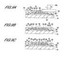
- FIG. 8A to FIG. 8Dare diagrams of the manufacturing steps of a semiconductor device according to this embodiment. They show cross-sections of the main steps.
- FIG. 9A to FIG. 9Care diagrams of manufacturing steps subsequent to FIG. 8 D.
- rearrangement sheet 78 provided with conductive metallic patterns 84is stuck onto insulating sheet 82 in a region of the upper surface of semiconductor element 76 where the plurality of bonding pads 74 are provided, which is exposed from bonding pads 74 (FIG. 8 A).
- Conductive metallic patterns 84 of rearrangement sheet 78are constituted by rearrangement posts 86 , wire connection portions 88 , and rewiring leads 90 that connect rearrangement posts 86 and wire connection portions 88 (see FIG. 7 C).
- bonding pads 74 and wire connection portions 88 of conductive metallic patterns 84are connected by fine metallic leads 92 .
- connectionis performed using the wire bond launching system.
- Metal balls 96 of Auare formed on bonding pads 74 . Bonding with wire connection portions 88 is performed such that the Au wires 92 are pulled up from these metal balls 96 (FIG. 8 B).
- conductive posts 94are formed by stud bumps produced by wire bonds, on the rearrangement posts 86 , of the conductive metallic patterns 84 .
- stud bumps made of Auare formed by wire bonds as conductive posts 94 (FIG. 8 C).
- sealing portion 80is formed by sealing using molded resin such that the bonding pads 74 on the upper surface of semiconductor element 76 , rearrangement sheet 78 , fine metallic wires 92 and conductive posts 94 are covered (FIG. 8 D).
- FIG. 9Ais a cross-sectional view of the structure during the grinding process.
- FIG. 9Bis a cross-sectional view of the structure immediately after completion of grinding.
- solder balls 98are formed on the upper surface of the exposed conductive posts 94 (FIG. 9 C).
- connection of the wire connection portions 88 and bonding pads 74is effected using the wire bond launching system.
- stud bumps constituting conductive posts 94are formed on rearrangement posts 86 by continuous wire bonding.
- Formation of these conductive posts 94was conventionally effected using the electrolytic plating method.
- the electrolytic plating methodIn simple terms, after forming a mask such that only the rearrangement posts are exposed, for example, Cu is plated onto the rearrangement posts by electrolytic plating. Next, the mask is removed.
- the step of forming conductive posts 94can be performed using wire bonding continuously from the step of connecting wire connection portions 88 and bonding pads 74 . Consequently, since the steps of mask formation and plating film formation are unnecessary, manufacturing costs can be made lower than conventional art.
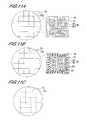
- FIG. 10A to FIG. 10Dare step diagrams illustrating the steps of manufacture of a wafer-level CSP according to this embodiment.
- FIG. 11A to FIG. 11Care manufacturing step diagrams subsequent to FIG. 10 D.
- FIG. 10A to FIG. 10Dshow views considered to be easy to understand, of plane views and cross-sectional views seen from above the structure during the course of its manufacture.
- FIG. 11A to FIG. 11Cshow a semiconductor wafer in plane view seen from above.
- FIG. 11 A and FIG. 11Bare views which, combined, show to a larger scale the upper surface of a single element of the plurality of semiconductor elements on the semiconductor wafer.
- insulating film 82 xis an insulating adhesive film.
- Insulating adhesive film 82 xis for example a film (semi-cured film) in a condition in which the curing reaction is not completed, obtained by curing a mixed material consisting of liquid epoxy resin and polyimide resin at ordinary temperature (room temperature) or low temperature (40 to 50° C.).
- Conductive metallic patterns 84are patterns corresponding to the shape of rearrangement posts 86 , wire connection portions 88 , and rewiring leads 90 that connect rearrangement posts 86 and wire connection portions 88 (see FIG. 7 C). Next, conductive metallic patterns 84 are formed using this mask. These conductive metallic patterns 84 may be formed solely by wiring metallic patterns, or may be constituted by conductive metal plated patterns, or may be constituted by wiring metallic patterns and conductive metal plated patterns partially formed on the wiring metallic patterns (FIG. 10 A).
- insulating adhesive film 82 x on which the conductive metallic patterns 84 are formedis divided up into each rewiring sheet 78 using an ordinary dicing machine.
- insulating adhesive film 82 x provided with conductive metallic patterns 84is fixed onto scribe ring 52 by means of scribing tape 54 (FIG. 10 B). Next, this is divided up into the rearrangement sheets 78 (FIG. 10 C).
- pushing-up pin 58 of pushing-up mechanism component 56 of the dicing machineis pushed up.
- the rearrangement sheets 78 formed by the dividing stepare pushed up.
- a rearrangement sheet 78is pulled up by means of collet 60 (FIG. 10 D).
- the divided rearrangement sheets 78are successively pulled up using this pushing-up mechanism component 56 and collet 60 .
- the rearrangement sheets 78 that have been pulled up by collet 60are stuck onto each of the semiconductor elements 76 of semiconductor wafer 102 .
- a plurality of bonding pads 74are formed on each semiconductor element 76 .
- Rearrangement sheets 78are stuck onto the regions where bonding pads 74 of semiconductor elements 76 are not formed (FIG. 11 A).
- bonding pads 74 on semiconductor element 76 and wire connection portions 88 of rearrangement sheets 78are connected by metallic wires 92 using the wire bond launching system.
- conductive posts 94are formed by stud bumps produced by existing wire bonds on the rearrangement posts 86 of rearrangement sheets 78 (see FIG. 11 B and FIG. 7 C).
- molded resin 104is formed on the entire upper surface of semiconductor wafer 102 .
- the rearrangement sheets 78 on the individual semiconductor elements 76 , metal wires 92 and stud bumps (conductive posts) 94 on the upper surface of the semiconductor wafer 102are thereby covered by molded resin 104 (FIG. 11 C).
- solder balls 98are formed on the upper surface of stud bumps 94 . These solder balls 98 constitute the electrodes for external connection (see FIG. 9 ).
- Semiconductor wafer 102is then fixed by means of scribing tape to the scribe ring, using a dicing machine. Next, it is divided up into the respective semiconductor elements 72 .
- the semiconductor device 72 of the fourth embodimentis manufactured at wafer level by going through the above steps.
- the semiconductor devices 72can be formed together in the condition of semiconductor wafer 102 .
- a considerable shortening of manufacturing timecan thereby be achieved, making it possible to achieve a considerable reduction in semiconductor device manufacturing costs.
- the first to the third embodiments described aboveare semiconductor devices of a type in which semiconductor elements are laminated, electrical connection between respective elements not being performed; however, the present invention is not restricted to such a construction. Specifically, the present invention can of course be applied also to semiconductor devices of a construction in which first elements and second elements are electrically connected, for example by wire-bonding, bonding pads of the first element and bonding pads of the second element. Also, the laminated semiconductor elements are not restricted to two, but application is also possible to devices in which further lamination is effected.
- a rearrangement sheet according to the present inventioncomprises an insulating sheet and conductive metallic patterns formed on the insulating sheet.
- a rearrangement sheetis interposed between the first element and second element of a construction obtained by laminating a first element and second element in that order on a substrate.
- bonding posts formed on the substrate and bonding pads of the first element and bonding pads of the second elementmust be respectively connected, first of all, connection is effected between the bonding posts and conductive metallic patterns of the rearrangement sheet. Next, these conductive metallic patterns and the bonding pads of the second element are connected.
- the bonding posts and bonding pads of the first elementare produced by wire bonding, in the same way as normally.
- connection between the bonding pads and bonding posts of the second elementcan be effected irrespective of the position of the metal wires that effect connection between the bonding pads and bonding posts of the first element. Consequently, by means of the rearrangement is sheet according to the present invention, for example in the example described above, rearrangement of the bonding pads of the second element can easily be performed. The degrees of design freedom of the second element can therefore be increased.
- the rearrangement sheetis provided in the regions where bonding pads are not formed of a semiconductor element equipped with a plurality of bonding pads.
- the conductive metallic patterns of the rearrangement sheetare constituted by for example rearrangement posts of the same number as the bonding pads, wire connection portions of the same number as the bonding pads, and rewiring leads that connect the rearrangement posts and the wire connection portions.
- the wire connection portionscan be formed in positions of the rearrangement sheet where connection with the bonding pads is easy. The bonding pads and the wire connection portions can therefore easily be connected by wire bonding.
- Conductive postsare provided on the rearrangement posts connected by the wire connection portions and rewiring leads.
- the upper surface of the semiconductor elementis sealed such that the upper surfaces of these conductive posts are exposed. In this way, the bonding pads of the semiconductor device can easily be rearranged on the conductive posts that are exposed from the sealed portion.
- Rearrangement of the electrodes onto the conductive metal patternscan therefore easily be performed by sticking rearrangement sheets formed with conductive metallic patterns according to the present invention at desired positions on the under-layer where the electrodes that are to be rearranged are provided.
Landscapes
- Engineering & Computer Science (AREA)
- Microelectronics & Electronic Packaging (AREA)
- Computer Hardware Design (AREA)
- Power Engineering (AREA)
- Physics & Mathematics (AREA)
- Condensed Matter Physics & Semiconductors (AREA)
- General Physics & Mathematics (AREA)
- Geometry (AREA)
- Wire Bonding (AREA)
Abstract
Description
Claims (30)
Priority Applications (2)
| Application Number | Priority Date | Filing Date | Title |
|---|---|---|---|
| US10/866,697US7435626B2 (en) | 2001-03-05 | 2004-06-15 | Rearrangement sheet, semiconductor device and method of manufacturing thereof |
| US12/153,501US20090031563A1 (en) | 2001-03-05 | 2008-05-20 | Rearrangement sheet, semiconductor device and method of manufacturing thereof |
Applications Claiming Priority (2)
| Application Number | Priority Date | Filing Date | Title |
|---|---|---|---|
| JP2001-060348 | 2001-03-05 | ||
| JP2001060348AJP4780844B2 (en) | 2001-03-05 | 2001-03-05 | Semiconductor device |
Related Child Applications (1)
| Application Number | Title | Priority Date | Filing Date |
|---|---|---|---|
| US10/866,697DivisionUS7435626B2 (en) | 2001-03-05 | 2004-06-15 | Rearrangement sheet, semiconductor device and method of manufacturing thereof |
Publications (2)
| Publication Number | Publication Date |
|---|---|
| US20020121686A1 US20020121686A1 (en) | 2002-09-05 |
| US6787915B2true US6787915B2 (en) | 2004-09-07 |
Family
ID=18919786
Family Applications (3)
| Application Number | Title | Priority Date | Filing Date |
|---|---|---|---|
| US09/930,710Expired - Fee RelatedUS6787915B2 (en) | 2001-03-05 | 2001-08-16 | Rearrangement sheet, semiconductor device and method of manufacturing thereof |
| US10/866,697Expired - Fee RelatedUS7435626B2 (en) | 2001-03-05 | 2004-06-15 | Rearrangement sheet, semiconductor device and method of manufacturing thereof |
| US12/153,501AbandonedUS20090031563A1 (en) | 2001-03-05 | 2008-05-20 | Rearrangement sheet, semiconductor device and method of manufacturing thereof |
Family Applications After (2)
| Application Number | Title | Priority Date | Filing Date |
|---|---|---|---|
| US10/866,697Expired - Fee RelatedUS7435626B2 (en) | 2001-03-05 | 2004-06-15 | Rearrangement sheet, semiconductor device and method of manufacturing thereof |
| US12/153,501AbandonedUS20090031563A1 (en) | 2001-03-05 | 2008-05-20 | Rearrangement sheet, semiconductor device and method of manufacturing thereof |
Country Status (2)
| Country | Link |
|---|---|
| US (3) | US6787915B2 (en) |
| JP (1) | JP4780844B2 (en) |
Cited By (31)
| Publication number | Priority date | Publication date | Assignee | Title |
|---|---|---|---|---|
| US20040063242A1 (en)* | 2002-09-17 | 2004-04-01 | Chippac, Inc. | Semiconductor multi-package module having package stacked over ball grid array package and having wire bond interconnect between stacked packages |
| US20040061213A1 (en)* | 2002-09-17 | 2004-04-01 | Chippac, Inc. | Semiconductor multi-package module having package stacked over die-up flip chip ball grid array package and having wire bond interconnect between stacked packages |
| US20050062166A1 (en)* | 2003-09-19 | 2005-03-24 | In-Ku Kang | Single chip and stack-type chip semiconductor package and method of manufacturing the same |
| US20050133916A1 (en)* | 2003-12-17 | 2005-06-23 | Stats Chippac, Inc | Multiple chip package module having inverted package stacked over die |
| US20060012018A1 (en)* | 2004-07-13 | 2006-01-19 | Chippac, Inc. | Semiconductor multipackage module including die and inverted land grid array package stacked over ball grid array package |
| US7053476B2 (en) | 2002-09-17 | 2006-05-30 | Chippac, Inc. | Semiconductor multi-package module having package stacked over die-down flip chip ball grid array package and having wire bond interconnect between stacked packages |
| US20060118945A1 (en)* | 2004-12-08 | 2006-06-08 | Ives Fred H | Low cost hermetic ceramic microcircuit package |
| US20060125070A1 (en)* | 2004-12-10 | 2006-06-15 | Gwang-Man Lim | Semiconductor package, manufacturing method thereof and IC chip |
| US7064426B2 (en) | 2002-09-17 | 2006-06-20 | Chippac, Inc. | Semiconductor multi-package module having wire bond interconnect between stacked packages |
| US20060220210A1 (en)* | 2005-03-31 | 2006-10-05 | Stats Chippac Ltd. | Semiconductor assembly including chip scale package and second substrate and having exposed substrate surfaces on upper and lower sides |
| US20060220209A1 (en)* | 2005-03-31 | 2006-10-05 | Stats Chippac Ltd. | Semiconductor stacked package assembly having exposed substrate surfaces on upper and lower sides |
| US20060244117A1 (en)* | 2005-04-29 | 2006-11-02 | Stats Chippac, Ltd. | Semiconductor package including second substrate and having exposed substrate surfaces on upper and lower sides |
| US20060249851A1 (en)* | 2005-05-05 | 2006-11-09 | Stats Chippac Ltd. | Multiple Chip Package Module Including Die Stacked Over Encapsulated Package |
| US20060284299A1 (en)* | 2005-06-20 | 2006-12-21 | Stats Chippac Ltd. | Module Having Stacked Chip Scale Semiconductor Packages |
| US20070018339A1 (en)* | 2005-07-20 | 2007-01-25 | Fujitsu Limited | Relay board and semiconductor device having the relay board |
| US20070111388A1 (en)* | 2002-10-08 | 2007-05-17 | Chippac, Inc. | Semiconductor Multi-Package Module Having Inverted Second Package Stacked Over Die-Up Flip-Chip Ball Grid Array (BGA) Package |
| US7435626B2 (en)* | 2001-03-05 | 2008-10-14 | Oki Electric Industry Co., Ltd. | Rearrangement sheet, semiconductor device and method of manufacturing thereof |
| US20080315439A1 (en)* | 2005-07-14 | 2008-12-25 | Chipmos Technologies Inc. | Quad flat non-leaded chip package |
| US20090242268A1 (en)* | 2008-03-31 | 2009-10-01 | Nec Electronics Corporation | Semiconductor device capable of switching operation modes |
| US7652376B2 (en) | 2006-01-04 | 2010-01-26 | Stats Chippac Ltd. | Integrated circuit package system including stacked die |
| US7687315B2 (en) | 2005-04-29 | 2010-03-30 | Stats Chippac Ltd. | Stacked integrated circuit package system and method of manufacture therefor |
| US7750482B2 (en) | 2006-02-09 | 2010-07-06 | Stats Chippac Ltd. | Integrated circuit package system including zero fillet resin |
| US7749807B2 (en) | 2003-04-04 | 2010-07-06 | Chippac, Inc. | Method of fabricating a semiconductor multipackage module including a processor and memory package assemblies |
| US7768125B2 (en) | 2006-01-04 | 2010-08-03 | Stats Chippac Ltd. | Multi-chip package system |
| US20100244268A1 (en)* | 2006-06-29 | 2010-09-30 | Jiamiao Tang | Apparatus, system, and method for wireless connection in integrated circuit packages |
| US7855100B2 (en) | 2005-03-31 | 2010-12-21 | Stats Chippac Ltd. | Integrated circuit package system with an encapsulant cavity and method of fabrication thereof |
| US8030134B2 (en) | 2004-05-24 | 2011-10-04 | Chippac, Inc. | Stacked semiconductor package having adhesive/spacer structure and insulation |
| US20120261181A1 (en)* | 2009-05-22 | 2012-10-18 | Koichi Izawa | Electromagnetic shielding method and electromagnetic shielding film |
| US8552551B2 (en) | 2004-05-24 | 2013-10-08 | Chippac, Inc. | Adhesive/spacer island structure for stacking over wire bonded die |
| US8623704B2 (en) | 2004-05-24 | 2014-01-07 | Chippac, Inc. | Adhesive/spacer island structure for multiple die package |
| US8704349B2 (en) | 2006-02-14 | 2014-04-22 | Stats Chippac Ltd. | Integrated circuit package system with exposed interconnects |
Families Citing this family (12)
| Publication number | Priority date | Publication date | Assignee | Title |
|---|---|---|---|---|
| US8089142B2 (en)* | 2002-02-13 | 2012-01-03 | Micron Technology, Inc. | Methods and apparatus for a stacked-die interposer |
| US7071421B2 (en) | 2003-08-29 | 2006-07-04 | Micron Technology, Inc. | Stacked microfeature devices and associated methods |
| JP4707548B2 (en) | 2005-12-08 | 2011-06-22 | 富士通セミコンダクター株式会社 | Semiconductor device and manufacturing method of semiconductor device |
| JP2010238996A (en)* | 2009-03-31 | 2010-10-21 | Sanyo Electric Co Ltd | Method of manufacturing semiconductor module |
| US20110084374A1 (en)* | 2009-10-08 | 2011-04-14 | Jen-Chung Chen | Semiconductor package with sectioned bonding wire scheme |
| US8522426B2 (en)* | 2010-06-05 | 2013-09-03 | Raytheon Company | Vent blocking on vented ball grid arrays to provide a cleaner solution barrier |
| US20130000968A1 (en)* | 2011-06-30 | 2013-01-03 | Broadcom Corporation | 1-Layer Interposer Substrate With Through-Substrate Posts |
| JP5748621B2 (en)* | 2011-09-12 | 2015-07-15 | ルネサスエレクトロニクス株式会社 | Semiconductor chip |
| US20130214408A1 (en)* | 2012-02-21 | 2013-08-22 | Broadcom Corporation | Interposer Having Conductive Posts |
| US9406660B2 (en) | 2014-04-29 | 2016-08-02 | Micron Technology, Inc. | Stacked semiconductor die assemblies with die support members and associated systems and methods |
| CN110071063B (en)* | 2019-06-03 | 2024-08-23 | 马鞍山荣泰科技有限公司 | Automatic arranging device for quartz wafers |
| CN118136747A (en)* | 2024-03-25 | 2024-06-04 | 佛山市国星光电股份有限公司 | A packaging method and packaging structure of an integrated chip |
Citations (10)
| Publication number | Priority date | Publication date | Assignee | Title |
|---|---|---|---|---|
| US5012323A (en)* | 1989-11-20 | 1991-04-30 | Micron Technology, Inc. | Double-die semiconductor package having a back-bonded die and a face-bonded die interconnected on a single leadframe |
| US5502289A (en)* | 1992-05-22 | 1996-03-26 | National Semiconductor Corporation | Stacked multi-chip modules and method of manufacturing |
| US5903049A (en)* | 1997-10-29 | 1999-05-11 | Mitsubishi Denki Kabushiki Kaisha | Semiconductor module comprising semiconductor packages |
| US5953213A (en)* | 1996-08-09 | 1999-09-14 | Robert Bosch Gmbh | Multichip module |
| US6222265B1 (en)* | 1997-03-10 | 2001-04-24 | Micron Technology, Inc. | Method of constructing stacked packages |
| US6359340B1 (en)* | 2000-07-28 | 2002-03-19 | Advanced Semiconductor Engineering, Inc. | Multichip module having a stacked chip arrangement |
| US6407450B1 (en)* | 1999-07-15 | 2002-06-18 | Altera Corporation | Semiconductor package with universal substrate for electrically interfacing with different sized chips that have different logic functions |
| US6407456B1 (en)* | 1996-02-20 | 2002-06-18 | Micron Technology, Inc. | Multi-chip device utilizing a flip chip and wire bond assembly |
| US6414384B1 (en)* | 2000-12-22 | 2002-07-02 | Silicon Precision Industries Co., Ltd. | Package structure stacking chips on front surface and back surface of substrate |
| US6476500B2 (en)* | 2000-07-25 | 2002-11-05 | Nec Corporation | Semiconductor device |
Family Cites Families (39)
| Publication number | Priority date | Publication date | Assignee | Title |
|---|---|---|---|---|
| US4446477A (en)* | 1981-08-21 | 1984-05-01 | Sperry Corporation | Multichip thin film module |
| US4663186A (en)* | 1986-04-24 | 1987-05-05 | International Business Machines Corporation | Screenable paste for use as a barrier layer on a substrate during maskless cladding |
| JP2815176B2 (en)* | 1989-06-08 | 1998-10-27 | ティーディーケイ株式会社 | Slider, head and recording / reproducing device |
| JPH04284663A (en)* | 1991-03-13 | 1992-10-09 | Toshiba Corp | semiconductor equipment |
| US5438224A (en)* | 1992-04-23 | 1995-08-01 | Motorola, Inc. | Integrated circuit package having a face-to-face IC chip arrangement |
| US5612576A (en)* | 1992-10-13 | 1997-03-18 | Motorola | Self-opening vent hole in an overmolded semiconductor device |
| US5700697A (en)* | 1993-02-01 | 1997-12-23 | Silicon Packaging Technology | Method for packaging an integrated circuit using a reconstructed package |
| US5353498A (en)* | 1993-02-08 | 1994-10-11 | General Electric Company | Method for fabricating an integrated circuit module |
| JP3150253B2 (en)* | 1994-07-22 | 2001-03-26 | 三菱電機株式会社 | Semiconductor device, its manufacturing method and mounting method |
| US5567654A (en)* | 1994-09-28 | 1996-10-22 | International Business Machines Corporation | Method and workpiece for connecting a thin layer to a monolithic electronic module's surface and associated module packaging |
| US5821608A (en)* | 1995-09-08 | 1998-10-13 | Tessera, Inc. | Laterally situated stress/strain relieving lead for a semiconductor chip package |
| US5844297A (en)* | 1995-09-26 | 1998-12-01 | Symbios, Inc. | Antifuse device for use on a field programmable interconnect chip |
| US5650667A (en)* | 1995-10-30 | 1997-07-22 | National Semiconductor Corporation | Process of forming conductive bumps on the electrodes of semiconductor chips using lapping and the bumps thereby created |
| TW398165B (en)* | 1997-03-03 | 2000-07-11 | Hitachi Chemical Co Ltd | Circuit boards using heat resistant resin for adhesive layers |
| JP3481444B2 (en)* | 1998-01-14 | 2003-12-22 | シャープ株式会社 | Semiconductor device and manufacturing method thereof |
| JPH11265975A (en)* | 1998-03-17 | 1999-09-28 | Mitsubishi Electric Corp | Multilayer integrated circuit device |
| US5854507A (en)* | 1998-07-21 | 1998-12-29 | Hewlett-Packard Company | Multiple chip assembly |
| JP3516592B2 (en)* | 1998-08-18 | 2004-04-05 | 沖電気工業株式会社 | Semiconductor device and manufacturing method thereof |
| US6291881B1 (en)* | 1999-03-04 | 2001-09-18 | United Microelectronics Corp. | Dual silicon chip package |
| KR100543428B1 (en)* | 1999-06-18 | 2006-01-20 | 히다치 가세고교 가부시끼가이샤 | Adhesive-bonded substrate, semiconductor mounting wiring board with adhesive member and semiconductor device using same |
| JP3304921B2 (en)* | 1999-06-18 | 2002-07-22 | 日本電気株式会社 | Semiconductor storage device |
| JP2001077298A (en)* | 1999-09-08 | 2001-03-23 | Mitsui High Tec Inc | Multi-chip package |
| US6511901B1 (en)* | 1999-11-05 | 2003-01-28 | Atmel Corporation | Metal redistribution layer having solderable pads and wire bondable pads |
| JP3798597B2 (en)* | 1999-11-30 | 2006-07-19 | 富士通株式会社 | Semiconductor device |
| JP2001185651A (en)* | 1999-12-27 | 2001-07-06 | Matsushita Electronics Industry Corp | Semiconductor device and manufacturing method therefor |
| JP4251421B2 (en)* | 2000-01-13 | 2009-04-08 | 新光電気工業株式会社 | Manufacturing method of semiconductor device |
| JP3386029B2 (en)* | 2000-02-09 | 2003-03-10 | 日本電気株式会社 | Flip chip type semiconductor device and manufacturing method thereof |
| US6717245B1 (en)* | 2000-06-02 | 2004-04-06 | Micron Technology, Inc. | Chip scale packages performed by wafer level processing |
| JP2002076250A (en)* | 2000-08-29 | 2002-03-15 | Nec Corp | Semiconductor device |
| JP4570809B2 (en)* | 2000-09-04 | 2010-10-27 | 富士通セミコンダクター株式会社 | Multilayer semiconductor device and manufacturing method thereof |
| JP4780844B2 (en)* | 2001-03-05 | 2011-09-28 | Okiセミコンダクタ株式会社 | Semiconductor device |
| US20030042587A1 (en)* | 2001-08-31 | 2003-03-06 | Tsung-Jen Lee | IC packaging and manufacturing methods |
| US6847105B2 (en)* | 2001-09-21 | 2005-01-25 | Micron Technology, Inc. | Bumping technology in stacked die configurations |
| US6555917B1 (en)* | 2001-10-09 | 2003-04-29 | Amkor Technology, Inc. | Semiconductor package having stacked semiconductor chips and method of making the same |
| US20030111720A1 (en)* | 2001-12-18 | 2003-06-19 | Tan Lan Chu | Stacked die semiconductor device |
| TWI268581B (en)* | 2002-01-25 | 2006-12-11 | Advanced Semiconductor Eng | Stack type flip-chip package including a substrate board, a first chip, a second chip, multiple conductive wire, an underfill, and a packaging material |
| US8089142B2 (en)* | 2002-02-13 | 2012-01-03 | Micron Technology, Inc. | Methods and apparatus for a stacked-die interposer |
| US6885093B2 (en)* | 2002-02-28 | 2005-04-26 | Freescale Semiconductor, Inc. | Stacked die semiconductor device |
| TW200637017A (en)* | 2005-04-14 | 2006-10-16 | Chipmos Technologies Inc | Image sensor module package |
- 2001
- 2001-03-05JPJP2001060348Apatent/JP4780844B2/ennot_activeExpired - Fee Related
- 2001-08-16USUS09/930,710patent/US6787915B2/ennot_activeExpired - Fee Related
- 2004
- 2004-06-15USUS10/866,697patent/US7435626B2/ennot_activeExpired - Fee Related
- 2008
- 2008-05-20USUS12/153,501patent/US20090031563A1/ennot_activeAbandoned
Patent Citations (10)
| Publication number | Priority date | Publication date | Assignee | Title |
|---|---|---|---|---|
| US5012323A (en)* | 1989-11-20 | 1991-04-30 | Micron Technology, Inc. | Double-die semiconductor package having a back-bonded die and a face-bonded die interconnected on a single leadframe |
| US5502289A (en)* | 1992-05-22 | 1996-03-26 | National Semiconductor Corporation | Stacked multi-chip modules and method of manufacturing |
| US6407456B1 (en)* | 1996-02-20 | 2002-06-18 | Micron Technology, Inc. | Multi-chip device utilizing a flip chip and wire bond assembly |
| US5953213A (en)* | 1996-08-09 | 1999-09-14 | Robert Bosch Gmbh | Multichip module |
| US6222265B1 (en)* | 1997-03-10 | 2001-04-24 | Micron Technology, Inc. | Method of constructing stacked packages |
| US5903049A (en)* | 1997-10-29 | 1999-05-11 | Mitsubishi Denki Kabushiki Kaisha | Semiconductor module comprising semiconductor packages |
| US6407450B1 (en)* | 1999-07-15 | 2002-06-18 | Altera Corporation | Semiconductor package with universal substrate for electrically interfacing with different sized chips that have different logic functions |
| US6476500B2 (en)* | 2000-07-25 | 2002-11-05 | Nec Corporation | Semiconductor device |
| US6359340B1 (en)* | 2000-07-28 | 2002-03-19 | Advanced Semiconductor Engineering, Inc. | Multichip module having a stacked chip arrangement |
| US6414384B1 (en)* | 2000-12-22 | 2002-07-02 | Silicon Precision Industries Co., Ltd. | Package structure stacking chips on front surface and back surface of substrate |
Cited By (81)
| Publication number | Priority date | Publication date | Assignee | Title |
|---|---|---|---|---|
| US20090031563A1 (en)* | 2001-03-05 | 2009-02-05 | Yasufumi Uchida | Rearrangement sheet, semiconductor device and method of manufacturing thereof |
| US7435626B2 (en)* | 2001-03-05 | 2008-10-14 | Oki Electric Industry Co., Ltd. | Rearrangement sheet, semiconductor device and method of manufacturing thereof |
| US20040063242A1 (en)* | 2002-09-17 | 2004-04-01 | Chippac, Inc. | Semiconductor multi-package module having package stacked over ball grid array package and having wire bond interconnect between stacked packages |
| US20040061213A1 (en)* | 2002-09-17 | 2004-04-01 | Chippac, Inc. | Semiconductor multi-package module having package stacked over die-up flip chip ball grid array package and having wire bond interconnect between stacked packages |
| US20100200966A1 (en)* | 2002-09-17 | 2010-08-12 | Marcos Karnezos | Semiconductor multi-package module having package stacked over die-up flip chip ball grid array package and having wire bond interconnect between stacked packages |
| US7053476B2 (en) | 2002-09-17 | 2006-05-30 | Chippac, Inc. | Semiconductor multi-package module having package stacked over die-down flip chip ball grid array package and having wire bond interconnect between stacked packages |
| US8143100B2 (en) | 2002-09-17 | 2012-03-27 | Chippac, Inc. | Method of fabricating a semiconductor multi-package module having wire bond interconnect between stacked packages |
| US7279361B2 (en) | 2002-09-17 | 2007-10-09 | Chippac, Inc. | Method for making a semiconductor multi-package module having wire bond interconnect between stacked packages |
| US7064426B2 (en) | 2002-09-17 | 2006-06-20 | Chippac, Inc. | Semiconductor multi-package module having wire bond interconnect between stacked packages |
| US20060172463A1 (en)* | 2002-09-17 | 2006-08-03 | Chippac, Inc. | Semiconductor multi-package module having wire bond interconnect between stacked packages |
| US20060170091A1 (en)* | 2002-09-17 | 2006-08-03 | Chippac, Inc. | Semiconductor multi-package module having package stacked over die-down flip chip ball grid array package and having wire bond interconnect between stacked packages |
| US7682873B2 (en) | 2002-09-17 | 2010-03-23 | Chippac, Inc. | Semiconductor multi-package module having package stacked over die-down flip chip ball grid array package and having wire bond interconnect between stacked packages |
| US7205647B2 (en) | 2002-09-17 | 2007-04-17 | Chippac, Inc. | Semiconductor multi-package module having package stacked over ball grid array package and having wire bond interconnect between stacked packages |
| US7935572B2 (en) | 2002-09-17 | 2011-05-03 | Chippac, Inc. | Semiconductor multi-package module having package stacked over die-up flip chip ball grid array package and having wire bond interconnect between stacked packages |
| US20070111388A1 (en)* | 2002-10-08 | 2007-05-17 | Chippac, Inc. | Semiconductor Multi-Package Module Having Inverted Second Package Stacked Over Die-Up Flip-Chip Ball Grid Array (BGA) Package |
| US7358115B2 (en) | 2002-10-08 | 2008-04-15 | Chippac, Inc. | Method of fabricating a semiconductor assembly including chip scale package and second substrate with exposed substrate surfaces on upper and lower sides |
| US7687313B2 (en) | 2002-10-08 | 2010-03-30 | Stats Chippac Ltd. | Method of fabricating a semiconductor multi package module having an inverted package stacked over ball grid array (BGA) package |
| US7364946B2 (en) | 2002-10-08 | 2008-04-29 | Chippac, Inc. | Method of fabricating a semiconductor multi-package module having inverted land grid array (LGA) package stacked over ball grid array (BGA) package |
| US7351610B2 (en) | 2002-10-08 | 2008-04-01 | Chippac, Inc. | Method of fabricating a semiconductor multi-package module having a second package substrate with an exposed metal layer wire bonded to a first package substrate |
| US20070114648A1 (en)* | 2002-10-08 | 2007-05-24 | Chippac, Inc. | Semiconductor Stacked Multi-Package Module Having Inverted Second Package |
| US20070117267A1 (en)* | 2002-10-08 | 2007-05-24 | Chippac, Inc. | Semiconductor Multi-Package Module Having Inverted Land Grid Array (LGA) Package Stacked Over Ball Grid Array (BGA) Package |
| US7749807B2 (en) | 2003-04-04 | 2010-07-06 | Chippac, Inc. | Method of fabricating a semiconductor multipackage module including a processor and memory package assemblies |
| US20070102802A1 (en)* | 2003-09-19 | 2007-05-10 | Samsung Electronics Co., Ltd. | Single chip and stack-type chip semiconductor package and method of manufacturing the same |
| US20050062166A1 (en)* | 2003-09-19 | 2005-03-24 | In-Ku Kang | Single chip and stack-type chip semiconductor package and method of manufacturing the same |
| US7282431B2 (en) | 2003-09-19 | 2007-10-16 | Samsung Electronics Co., Ltd. | Single chip and stack-type chip semiconductor package and method of manufacturing the same |
| US7176558B2 (en)* | 2003-09-19 | 2007-02-13 | Samsung Electronics Co., Ltd. | Single chip and stack-type chip semiconductor package and method of manufacturing the same |
| US8970049B2 (en) | 2003-12-17 | 2015-03-03 | Chippac, Inc. | Multiple chip package module having inverted package stacked over die |
| US20050133916A1 (en)* | 2003-12-17 | 2005-06-23 | Stats Chippac, Inc | Multiple chip package module having inverted package stacked over die |
| US8552551B2 (en) | 2004-05-24 | 2013-10-08 | Chippac, Inc. | Adhesive/spacer island structure for stacking over wire bonded die |
| US8623704B2 (en) | 2004-05-24 | 2014-01-07 | Chippac, Inc. | Adhesive/spacer island structure for multiple die package |
| US8030134B2 (en) | 2004-05-24 | 2011-10-04 | Chippac, Inc. | Stacked semiconductor package having adhesive/spacer structure and insulation |
| US20070278658A1 (en)* | 2004-07-13 | 2007-12-06 | Stats Chippac Ltd. | Semiconductor multipackage module including die and inverted land grid array package stacked over ball grid array package |
| US7829382B2 (en) | 2004-07-13 | 2010-11-09 | Chippac, Inc. | Method for making semiconductor multipackage module including die and inverted land grid array package stacked over ball grid array package |
| US20060012018A1 (en)* | 2004-07-13 | 2006-01-19 | Chippac, Inc. | Semiconductor multipackage module including die and inverted land grid array package stacked over ball grid array package |
| US20100136744A1 (en)* | 2004-07-13 | 2010-06-03 | Marcos Karnezos | Method for making semiconductor multipackage module including die and inverted land grid array package stacked over ball grid array package |
| US7692279B2 (en) | 2004-07-13 | 2010-04-06 | Chippac, Inc. | Semiconductor multipackage module including die and inverted land grid array package stacked over ball grid array package |
| US7253511B2 (en) | 2004-07-13 | 2007-08-07 | Chippac, Inc. | Semiconductor multipackage module including die and inverted land grid array package stacked over ball grid array package |
| US20060118945A1 (en)* | 2004-12-08 | 2006-06-08 | Ives Fred H | Low cost hermetic ceramic microcircuit package |
| US20080145971A1 (en)* | 2004-12-10 | 2008-06-19 | Gwang-Man Lim | Semiconductor package, manufacturing method thereof and IC chip |
| US20080164596A1 (en)* | 2004-12-10 | 2008-07-10 | Gwang-Man Lim | Semiconductor package, manufacturing method thereof and IC chip |
| US7355274B2 (en)* | 2004-12-10 | 2008-04-08 | Samsung Electronics Co., Ltd. | Semiconductor package, manufacturing method thereof and IC chip |
| US20100164088A1 (en)* | 2004-12-10 | 2010-07-01 | Gwang-Man Lim | Semiconductor package, manufacturing method thereof and ic chip |
| US20060125070A1 (en)* | 2004-12-10 | 2006-06-15 | Gwang-Man Lim | Semiconductor package, manufacturing method thereof and IC chip |
| US7855100B2 (en) | 2005-03-31 | 2010-12-21 | Stats Chippac Ltd. | Integrated circuit package system with an encapsulant cavity and method of fabrication thereof |
| US7429787B2 (en) | 2005-03-31 | 2008-09-30 | Stats Chippac Ltd. | Semiconductor assembly including chip scale package and second substrate with exposed surfaces on upper and lower sides |
| US20060220210A1 (en)* | 2005-03-31 | 2006-10-05 | Stats Chippac Ltd. | Semiconductor assembly including chip scale package and second substrate and having exposed substrate surfaces on upper and lower sides |
| US20060220209A1 (en)* | 2005-03-31 | 2006-10-05 | Stats Chippac Ltd. | Semiconductor stacked package assembly having exposed substrate surfaces on upper and lower sides |
| US8309397B2 (en) | 2005-03-31 | 2012-11-13 | Stats Chippac Ltd. | Integrated circuit packaging system with a component in an encapsulant cavity and method of fabrication thereof |
| US8021924B2 (en) | 2005-03-31 | 2011-09-20 | Stats Chippac Ltd. | Encapsulant cavity integrated circuit package system and method of fabrication thereof |
| US7372141B2 (en) | 2005-03-31 | 2008-05-13 | Stats Chippac Ltd. | Semiconductor stacked package assembly having exposed substrate surfaces on upper and lower sides |
| US20060244117A1 (en)* | 2005-04-29 | 2006-11-02 | Stats Chippac, Ltd. | Semiconductor package including second substrate and having exposed substrate surfaces on upper and lower sides |
| US7687315B2 (en) | 2005-04-29 | 2010-03-30 | Stats Chippac Ltd. | Stacked integrated circuit package system and method of manufacture therefor |
| US7429786B2 (en) | 2005-04-29 | 2008-09-30 | Stats Chippac Ltd. | Semiconductor package including second substrate and having exposed substrate surfaces on upper and lower sides |
| US7582960B2 (en) | 2005-05-05 | 2009-09-01 | Stats Chippac Ltd. | Multiple chip package module including die stacked over encapsulated package |
| US20060249851A1 (en)* | 2005-05-05 | 2006-11-09 | Stats Chippac Ltd. | Multiple Chip Package Module Including Die Stacked Over Encapsulated Package |
| US7645634B2 (en) | 2005-06-20 | 2010-01-12 | Stats Chippac Ltd. | Method of fabricating module having stacked chip scale semiconductor packages |
| US20060284299A1 (en)* | 2005-06-20 | 2006-12-21 | Stats Chippac Ltd. | Module Having Stacked Chip Scale Semiconductor Packages |
| US7394148B2 (en) | 2005-06-20 | 2008-07-01 | Stats Chippac Ltd. | Module having stacked chip scale semiconductor packages |
| US7851896B2 (en)* | 2005-07-14 | 2010-12-14 | Chipmos Technologies Inc. | Quad flat non-leaded chip package |
| US20080315439A1 (en)* | 2005-07-14 | 2008-12-25 | Chipmos Technologies Inc. | Quad flat non-leaded chip package |
| US20070018339A1 (en)* | 2005-07-20 | 2007-01-25 | Fujitsu Limited | Relay board and semiconductor device having the relay board |
| US7608925B2 (en)* | 2005-07-20 | 2009-10-27 | Fujitsu Microelectronics Limited | Relay board with bonding pads connected by wirings |
| US7652376B2 (en) | 2006-01-04 | 2010-01-26 | Stats Chippac Ltd. | Integrated circuit package system including stacked die |
| US7768125B2 (en) | 2006-01-04 | 2010-08-03 | Stats Chippac Ltd. | Multi-chip package system |
| US7750482B2 (en) | 2006-02-09 | 2010-07-06 | Stats Chippac Ltd. | Integrated circuit package system including zero fillet resin |
| US8704349B2 (en) | 2006-02-14 | 2014-04-22 | Stats Chippac Ltd. | Integrated circuit package system with exposed interconnects |
| US8084867B2 (en)* | 2006-06-29 | 2011-12-27 | Intel Corporation | Apparatus, system, and method for wireless connection in integrated circuit packages |
| US8963333B2 (en) | 2006-06-29 | 2015-02-24 | Intel Corporation | Apparatus, system, and method for wireless connection in integrated circuit packages |
| US9837340B2 (en) | 2006-06-29 | 2017-12-05 | Intel Corporation | Apparatus, system, and method for wireless connection in integrated circuit packages |
| US9385094B2 (en) | 2006-06-29 | 2016-07-05 | Intel Corporation | Apparatus, system, and method for wireless connection in integrated circuit packages |
| US8513108B2 (en)* | 2006-06-29 | 2013-08-20 | Intel Corporation | Apparatus, system, and method for wireless connection in integrated circuit packages |
| US20120108053A1 (en)* | 2006-06-29 | 2012-05-03 | Jiamiao Tang | Apparatus, system, and method for wireless connection in integrated circuit packages |
| US20100244268A1 (en)* | 2006-06-29 | 2010-09-30 | Jiamiao Tang | Apparatus, system, and method for wireless connection in integrated circuit packages |
| US8981573B2 (en) | 2006-06-29 | 2015-03-17 | Intel Corporation | Apparatus, system, and method for wireless connection in integrated circuit packages |
| US20090242268A1 (en)* | 2008-03-31 | 2009-10-01 | Nec Electronics Corporation | Semiconductor device capable of switching operation modes |
| US7994437B2 (en) | 2008-03-31 | 2011-08-09 | Renesas Electronics Corporation | Semiconductor device capable of switching operation modes |
| US8633407B2 (en) | 2008-03-31 | 2014-01-21 | Renesas Electronics Corporation | Semiconductor device capable of switching operation modes |
| US8344269B2 (en) | 2008-03-31 | 2013-01-01 | Renesas Electronics Corporation | Semiconductor device capable of switching operation modes |
| US7763812B2 (en)* | 2008-03-31 | 2010-07-27 | Nec Electronics Corporation | Semiconductor device capable of switching operation modes |
| US8853562B2 (en)* | 2009-05-22 | 2014-10-07 | Sony Corporation | Electromagnetic shielding method and electromagnetic shielding film |
| US20120261181A1 (en)* | 2009-05-22 | 2012-10-18 | Koichi Izawa | Electromagnetic shielding method and electromagnetic shielding film |
Also Published As
| Publication number | Publication date |
|---|---|
| US7435626B2 (en) | 2008-10-14 |
| US20090031563A1 (en) | 2009-02-05 |
| JP2002261234A (en) | 2002-09-13 |
| JP4780844B2 (en) | 2011-09-28 |
| US20020121686A1 (en) | 2002-09-05 |
| US20040232539A1 (en) | 2004-11-25 |
Similar Documents
| Publication | Publication Date | Title |
|---|---|---|
| US6787915B2 (en) | Rearrangement sheet, semiconductor device and method of manufacturing thereof | |
| US6368896B2 (en) | Method of wafer level chip scale packaging | |
| US6911355B2 (en) | Semiconductor package having flex circuit with external contacts | |
| US6808962B2 (en) | Semiconductor device and method for fabricating the semiconductor device | |
| US6949470B2 (en) | Method for manufacturing circuit devices | |
| JPH0897217A (en) | Semiconductor device and manufacturing method thereof | |
| US6989291B2 (en) | Method for manufacturing circuit devices | |
| JP2001284381A (en) | Semiconductor device and method of manufacture | |
| US6936927B2 (en) | Circuit device having a multi-layer conductive path | |
| US7030033B2 (en) | Method for manufacturing circuit devices | |
| US6720209B2 (en) | Method for fabricating a circuit device | |
| US6883231B2 (en) | Method for fabricating a circuit device | |
| US6780676B2 (en) | Method for fabricating a circuit device | |
| JP3732378B2 (en) | Manufacturing method of semiconductor device | |
| US20040089946A1 (en) | Chip size semiconductor package structure | |
| JP3502056B2 (en) | Semiconductor device and laminated structure using the same | |
| JP3397045B2 (en) | Semiconductor device and manufacturing method thereof | |
| JP3674550B2 (en) | Semiconductor device | |
| JP2010287900A (en) | Semiconductor device | |
| JP3413413B2 (en) | Semiconductor element mounting substrate and method of manufacturing the same | |
| JP2004158596A (en) | Method for manufacturing circuit device | |
| JPH10303254A (en) | Tape carrier for mounting semiconductor element, and semiconductor device using the tape carrier | |
| JPH11340271A (en) | Method for manufacturing semiconductor device |
Legal Events
| Date | Code | Title | Description |
|---|---|---|---|
| AS | Assignment | Owner name:OKI ELECTRIC INDUSTRY CO., LTD., JAPAN Free format text:ASSIGNMENT OF ASSIGNORS INTEREST;ASSIGNORS:UCHIDA, YASUFUMI;SAEKI, YOSHIHIRO;REEL/FRAME:012105/0445 Effective date:20010719 | |
| FEPP | Fee payment procedure | Free format text:PAYOR NUMBER ASSIGNED (ORIGINAL EVENT CODE: ASPN); ENTITY STATUS OF PATENT OWNER: LARGE ENTITY | |
| FPAY | Fee payment | Year of fee payment:4 | |
| AS | Assignment | Owner name:OKI ELECTRIC INDUSTRY CO., LTD., JAPAN Free format text:ASSIGNMENT OF ASSIGNORS INTEREST;ASSIGNORS:UCHIDA, YASUFUMI;SAEKI, YOSHIHIRO;REEL/FRAME:021036/0915 Effective date:20010719 | |
| AS | Assignment | Owner name:OKI SEMICONDUCTOR CO., LTD., JAPAN Free format text:CHANGE OF NAME;ASSIGNOR:OKI ELECTRIC INDUSTRY CO., LTD.;REEL/FRAME:022043/0739 Effective date:20081001 Owner name:OKI SEMICONDUCTOR CO., LTD.,JAPAN Free format text:CHANGE OF NAME;ASSIGNOR:OKI ELECTRIC INDUSTRY CO., LTD.;REEL/FRAME:022043/0739 Effective date:20081001 | |
| REMI | Maintenance fee reminder mailed | ||
| LAPS | Lapse for failure to pay maintenance fees | ||
| STCH | Information on status: patent discontinuation | Free format text:PATENT EXPIRED DUE TO NONPAYMENT OF MAINTENANCE FEES UNDER 37 CFR 1.362 | |
| FP | Lapsed due to failure to pay maintenance fee | Effective date:20120907 |