US6787823B2 - Semiconductor device having cell-based basic element aggregate having protruding part in active region - Google Patents
Semiconductor device having cell-based basic element aggregate having protruding part in active regionDownload PDFInfo
- Publication number
- US6787823B2 US6787823B2US10/315,102US31510202AUS6787823B2US 6787823 B2US6787823 B2US 6787823B2US 31510202 AUS31510202 AUS 31510202AUS 6787823 B2US6787823 B2US 6787823B2
- Authority
- US
- United States
- Prior art keywords
- active regions
- protruding part
- type active
- protruding
- basic element
- Prior art date
- Legal status (The legal status is an assumption and is not a legal conclusion. Google has not performed a legal analysis and makes no representation as to the accuracy of the status listed.)
- Expired - Fee Related
Links
Images


Classifications
- H—ELECTRICITY
- H10—SEMICONDUCTOR DEVICES; ELECTRIC SOLID-STATE DEVICES NOT OTHERWISE PROVIDED FOR
- H10D—INORGANIC ELECTRIC SEMICONDUCTOR DEVICES
- H10D84/00—Integrated devices formed in or on semiconductor substrates that comprise only semiconducting layers, e.g. on Si wafers or on GaAs-on-Si wafers
- H10D84/90—Masterslice integrated circuits
- H10D84/903—Masterslice integrated circuits comprising field effect technology
- H10D84/907—CMOS gate arrays
Definitions
- the present inventionrelates to the configuration of a basic element aggregate to be incorporated into a large-scale semiconductor integrated circuit. More particularly, it relates to a cell-based basic element aggregate.
- LSIsSemi-custom LSIs are roughly classified into the following groups: PLD (programmable logic device), FPGA (field programmable gate array), gate array, and cell based IC (also referred to as a standard cell).
- PLDprogrammable logic device
- FPGAfield programmable gate array
- gate arraygate array
- cell based ICalso referred to as a standard cell
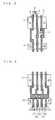
- FIG. 16is a plan view illustrating gate array.
- gate interconnect lines 100are shown to be equally spaced, namely, gate patterns (gate structures) are shown to be uniform according to the configuration of the gate array.
- An N-type impurity diffusion region, the gate interconnect line 100 , and another n-type impurity diffusion region adjacent to this gate interconnect line 100form a transistor.
- These n-type impurity diffusion regions adjacent to each other through the gate interconnect line 100are referred to as n-type active regions 101 .
- a plurality of p-type impurity diffusion regions arranged in the same manner as the plurality of n-type active regions 101are referred to as p-type active regions 102 .
- the gate interconnect line 100 , the n-type active region 101 , and the p-type active region 102are provided with contact holes 103 for interconnecting a plurality of transistors including the gate interconnect lines 100 , the n-type active regions 101 , and the p-type active regions 102 .
- FIG. 17is a plan view illustrating cell based design.
- gate patterns of gate interconnect lines 104 provided on active regionsare shown to be nonuniform. As a result, space in one chip can be used more effectively than the gate array.
- An n-type impurity diffusion region, the gate interconnect line 104 , and another n-type impurity diffusion region adjacent to this gate interconnect line 104form a transistor.
- n-type active regions 105These n-type impurity diffusion regions adjacent to each other through the gate interconnect line 104 are referred to as n-type active regions 105 .
- a plurality of p-type impurity diffusion regions arranged in the same manner as the plurality of n-type active regions 105are referred to as p-type active regions 106 .
- the gate interconnect line 104 , the n-type active region 105 , and the p-type active region 106are provided with contact holes 107 for interconnecting a plurality of transistors including the gate interconnect lines 104 , the n-type active regions 105 , and the p-type active regions 106 .
- the gate interconnect lines 104 provided on the n-type active regions 105 or on the p-type active regions 106may have nonuniformity in gate pattern (gate structure).
- gate patterngate pattern
- complicated processing using CAD systemis required in forming a mask, so that the gate interconnect lines 104 are uniform in finished gate pattern (gate structure).
- complicated processing using CAD systemcauses the problem that huge amount of time and costs are required.
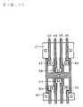
- gate patterns (structures) thereofmay be defined to be uniform in design stage. According to the cell based design in the background art shown in FIG. 17, however, uniformity of the gate patterns (gate structures) are not allowed according to whether the contact holes on the active regions are required or not.
- the p-type active regions 106can be defined to extend more widely as shown in FIG. 18, which in turn results in increase in area of the p-type active regions 106 and eventually, increase in area to be assigned exclusively to the basic element aggregate.
- the semiconductor integrated circuithas a cell-based basic element aggregate.
- the cell-based basic element aggregateincludes a first active region and a second active region provided on a semiconductor substrate, and a plurality of gate interconnect lines.
- the plurality of gate interconnect linesextend on the first and second active regions in a predetermined direction.
- the plurality of gate interconnect linesare equally spaced at least on the first and second active regions.
- At least one of the first and second active regionsis provided with at least one protruding part extending in the predetermined direction.
- the cell-based basic element aggregatefurther includes a contact hole provided to the at least one protruding part.
- At least one protruding partis provided to at least one of the first and second active regions. Therefore, uniformity of the gate interconnect lines in finished gate pattern (gate structure) is allowed on the first and second active regions after wafer processing requiring no complicated processing using CAD system. Further, there occurs no increase in area to be assigned exclusively to the basic element aggregate.
- FIG. 1is a plan view illustrating a basic element aggregate of a semiconductor integrated circuit according to a first preferred embodiment of the present invention
- FIGS. 2 and 3are plan views each illustrating a basic element aggregate of a semiconductor integrated circuit according to a modification of the first preferred embodiment of the present invention
- FIG. 4is a plan view illustrating a basic element aggregate of a semiconductor integrated circuit according to a second preferred embodiment of the present invention.
- FIGS. 5 and 6are plan views each illustrating a basic element aggregate of a semiconductor integrated circuit according to a modification of the second preferred embodiment of the present invention
- FIG. 7is a plan view illustrating a basic element aggregate of a semiconductor integrated circuit according to a third preferred embodiment of the present invention.
- FIGS. 8 through 15are plan views each illustrating a basic element aggregate of a semiconductor integrated circuit according to a modification of the third preferred embodiment of the present invention.
- FIG. 16is a plan view illustrating the background-art basic element aggregate of the semiconductor integrated circuit following gate array technology.
- FIGS. 17 and 18are plan views each illustrating the background-art basic element aggregate of the semiconductor integrated circuit following cell based design.
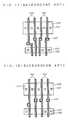
- FIG. 1is a plan view illustrating the basic element aggregate of a semiconductor integrated circuit according to the first preferred embodiment of the present invention. More particularly, FIG. 1 illustrates a part of the basic element aggregate including p-channel transistors and n-channel transistors.
- a p-type impurity diffusion region, a gate interconnect line, and another p-type impurity diffusion region adjacent to this gate interconnect lineform the p-channel transistor.
- These p-type impurity diffusion regions adjacent to each other through the gate interconnect lineare referred to as p-type active regions 1 (alternatively, as first or second active regions 1 ).
- n-type impurity diffusion regionan n-type impurity diffusion region, a gate interconnect line, and another n-type impurity diffusion region adjacent to this gate interconnect line form an n-channel transistor.
- n-type impurity diffusion regionsare referred to as n-type active regions 2 (alternatively, as second or first active regions 2 ).
- Three gate interconnect lines 3 , 4 and 5are provided on the p-type active regions 1 and on the n-type active regions 2 .
- the p-type active regions 1have protruding parts for holding therein contact holes 6 and 7 . These protruding parts are each arranged on the side opposite to that facing the n-type active regions 2 .
- the contact hole 6 in one protruding partis provided between the gate interconnect lines 3 and 4 .
- the contact hole 7 in the other protruding partis provided between the gate interconnect lines 4 and 5 .
- the contact holes 6 and 7are used for interconnecting a plurality of transistors to be defined in the p-type active regions 1 .
- the contact holes 6 and 7do not exist between the gate interconnect lines 3 , 4 and 5 defined on the p-type active regions 1 except for the protruding parts thereof. Without limited by the positions of the contact holes 6 and 7 , it is thus allowed to arrange the gate interconnect lines 3 , 4 and 6 on the p-type active regions 1 excluding the protruding parts thereof. As a result, the gate patterns (gate structures) of the gate interconnect lines 3 , 4 and 5 can be uniform on the p-type active regions 1 except for the protruding parts thereof. Further, the gate interconnect lines 3 , 4 and 5 are so formed to bypass the protruding parts.
- the configuration illustrated in FIG. 1allows the gate interconnect lines 3 , 4 and 5 to be uniform in finished gate pattern (gate structure) on the p-type active regions 1 after wafer processing requiring no complicated processing using CAD system. Further, the configuration in FIG. 1 requires no increase in area of the p-type active regions 1 . As a result, according to the first preferred embodiment, there occurs no increase in area to be assigned exclusively to the basic element aggregate.
- a width L1 of the protruding part for holding therein the contact hole 6is larger than a space L3 between the gate interconnect lines 3 and 4 on the p-type active regions 1 (namely, the space extending in a direction parallel to that of the width L1).
- a width L2 of the protruding part for holding therein the contact hole 7is larger than a space L4 between the gate interconnect lines 4 and 5 on the p-type active regions 1 .
- FIGS. 2 and 3are plan views each illustrating the basic element aggregate of a semiconductor integrated circuit according to the modification of the first preferred embodiment.
- the p-type active regions 1have protruding parts for holding therein contact holes 8 and 9 . These protruding parts are each arranged on the side facing the n-type active regions 2 (in FIG. 2, on the lower part of the p-type active region 1 ).
- the contact hole 8 in one protruding partis provided between the gate interconnect lines 3 and 4 .
- the contact hole 9 in the other protruding partis provided between the gate interconnect lines 4 and 5 .
- the same effects as obtained in the aggregate shown in FIG. 1are also realized.
- the p-type active regions 1have protruding parts for holding therein contact holes 10 and 11 .
- the protruding part to include therein the contact hole 10is arranged on the side opposite to that facing the n-type active regions 2
- the protruding part to include therein the contact hole 11is arranged on the side facing the n-type active regions 2 .
- the arrangement of the protruding parts for holding therein the contact holes 10 and 11is not limited to the one given in FIG. 3 . As long as one protruding part is provided with the p-type active region 1 on the side facing the n-type active regions 2 and other part is on the side opposite thereto, any arrangement may be applicable.
- the contact hole 10 in one protruding partis provided between the gate interconnect lines 3 and 4 .
- the contact hole 11 in the other protruding partis provided between the gate interconnect lines 4 and 5 .
- the same effects as obtained in the aggregate shown in FIG. 1are also realized. Further, the basic element aggregate in FIG. 3 improves flexibility in arrangement of the contact holes. As a result, flexibility in arrangement of interconnect lines to be connected to these contact holes can be also enhanced.
- FIG. 4is a plan view illustrating the basic element aggregate of a semiconductor integrated circuit according to the second preferred embodiment.
- P-type active regions 21 and n-type active regions 22are provided on a semiconductor substrate (not shown).
- a p-type impurity diffusion region, a gate interconnect line, and another p-type impurity diffusion region adjacent to this gate interconnect lineform a transistor.
- These p-type impurity diffusion regions adjacent to each other through the gate interconnect lineare referred to as the p-type active regions 21 (alternatively, as first or second active regions 21 ).
- n-type active regions 22a plurality of n-type impurity diffusion regions are referred to as the n-type active regions 22 (alternatively, second or first active regions 22 ).
- gate interconnect lines 23 , 24 , 25 and 26are provided on the p-type active regions 21 and on the n-type active regions 22 .
- the n-type active regions 22have protruding parts for holding therein contact holes 27 , 28 and 29 . These protruding parts are each arranged on the side opposite to that facing the p-type active regions 21 (in FIG. 4, on the lower part of the n-type active region 22 ).
- the contact hole 27 in one protruding partis provided between the gate interconnect lines 23 and 24 .
- the contact hole 28 in another protruding partis provided between the gate interconnect lines 24 and 25 .
- the contact hole 29 in another protruding partis provided between the gate interconnect lines 25 and 26 .
- the contact holes 27 , 28 and 29are used for interconnecting a plurality of transistors to be defined in the n-type active regions 22 .
- the contact holes 27 , 28 and 29do not exist between the gate interconnect lines 23 , 24 , 25 and 26 defined on the n-type active regions 22 except for the protruding parts thereof. Without limited by the positions of the contact holes 27 , 28 and 29 , it is thus allowed to arrange the gate interconnect lines 23 , 24 , 25 and 26 on the n-type active regions 22 excluding the protruding parts thereof. As a result, the gate patterns (gate structures) of the gate interconnect lines 23 , 24 , 25 and 26 can be uniform on the n-type active regions 22 except for the protruding parts thereof. Further, the gate interconnect lines 23 , 24 , 25 and 26 are so formed to bypass the protruding parts.
- the configuration illustrated in FIG. 4allows the gate interconnect lines 23 , 24 , 25 and 26 to be uniform in finished gate pattern (gate structure) on the n-type active regions 22 after wafer processing requiring no complicated processing using CAD system. Further, the configuration in FIG. 4 requires no increase in area of the n-type active regions 22 . As a result, according to the second preferred embodiment, there occurs no increase in area to be assigned exclusively to the basic element aggregate.
- FIGS. 5 and 6are plan views each illustrating the basic element aggregate of a semiconductor integrated according to the modification of the second preferred embodiment.
- the n-type active regions 22have protruding parts for holding therein contact holes 30 , 31 and 32 . These protruding parts are each arranged on the side facing the p-type active regions 21 (in FIG. 5, on the upper part of the n-type active region 22 ). According to the basic element aggregate shown in FIG. 5, the same effects as obtained in the aggregate shown in FIG. 4 are also realized.
- the n-type active regions 22have protruding parts for holding therein contact holes 33 , 34 and 35 .
- the protruding part to include therein the contact hole 33is arranged on the side opposite to that facing the p-type active regions 21
- the protruding parts to include therein the contact holes 34 and 35are each arranged on the side facing the p-type active regions 21 .
- the arrangement of the protruding parts for holding therein the contact holes 33 , 34 and 35is not limited to the one given in FIG. 6 . As long as one protruding part is provided with the n-type active region 22 on the side facing the p-type active regions 21 and other part is on the side opposite thereto, any arrangement may be applicable.
- the same effects as obtained in the aggregate shown in FIG. 4are also realized. Further, the basic element aggregate in FIG. 6 improves flexibility in arrangement of the contact holes. As a result, flexibility in arrangement of interconnect lines to be connected to these contact holes can be also enhanced.
- FIG. 7is a plan view illustrating the basic element aggregate of a semiconductor integrated circuit according to the third preferred embodiment.
- P-type active regions 41 and n-type active regions 42are provided on a semiconductor substrate (not shown).
- a p-type impurity diffusion region, a gate interconnect line, and another p-type impurity diffusion region adjacent to this gate interconnect lineform a transistor.
- These p-type impurity diffusion regions adjacent to each other through the gate interconnect lineare referred to as the p-type active regions 41 (alternatively, as first or second active regions 41 ).
- n-type active regions 42a plurality of n-type impurity diffusion regions are referred to as the n-type active regions 42 (alternatively, second or first active regions 42 ).
- gate interconnect lines 43 , 44 , 45 and 46are provided on the p-type active regions 41 and on the n-type active regions 42 .
- the p-type active regions 41have protruding parts for holding therein contact holes 47 , 48 and 49 . These protruding parts are each arranged on the side opposite to that facing the n-type active regions 42 (in FIG. 7, on the upper part of the p-type active region 41 ).
- the contact hole 47 in one protruding partis provided between the gate interconnect lines 43 and 44 .
- the contact hole 48 in another protruding partis provided between the gate interconnect lines 44 and 45 .
- the contact hole 49 in another protruding partis provided between the gate interconnect lines 45 and 46 .
- the contact holes 47 , 48 and 49are used for interconnecting a plurality of transistors to be defined in the p-type active regions 41 .
- the n-type active regions 42have protruding parts for holding therein contact holes 50 , 51 and 52 . These protruding parts are each arranged on the side opposite to that facing the p-type active regions 41 (in FIG. 7, on the lower part of the n-type active region 42 ).
- the contact hole 50 in one protruding partis provided between the gate interconnect lines 43 and 44 .
- the contact hole 51 in another protruding partis provided between the gate interconnect lines 44 and 45 .
- the contact hole 52 in another protruding partis provided between the gate interconnect lines 45 and 46 .
- the contact holes 50 , 51 and 52are used for interconnecting a plurality of transistors to be defined in the n-type active regions 42 .
- the contact holes 47 , 48 , 49 , 50 , 51 and 52do not exist between the gate interconnect lines 43 , 44 , 45 and 46 defined on the p-type active regions 41 and on the n-type active regions 42 except for their respective protruding parts. Without limited by the positions of the contact holes 47 , 48 , 49 , 50 , 51 and 52 , it is thus allowed to arrange the gate interconnect lines 43 , 44 , 45 and 46 on the p-type active regions 41 and on the n-type active regions 42 excluding their respective protruding parts.
- the gate patterns (gate structures) of the gate interconnect lines 43 , 44 , 45 and 46can be uniform on the p-type active regions 41 and on the n-type active regions 42 except for their respective protruding parts. Further, the gate interconnect lines 43 , 44 , 45 and 46 are so formed to bypass the protruding parts.
- the configuration illustrated in FIG. 7allows the gate interconnect lines 43 , 44 , 45 and 46 to be uniform in finished gate pattern (gate structure) on the p-type active regions 41 and on the n-type active regions 42 after wafer processing requiring no complicated processing using CAD system. Further, the configuration in FIG. 7 requires no increase in area of the p-type active regions 41 and of the n-type active regions 42 . As a result, according to the third preferred embodiment, there occurs no increase in area to be assigned exclusively to the basic element aggregate.
- FIGS. 8 through 15are plan views each illustrating the basic element aggregate of a semiconductor integrated circuit according to the modification of the third preferred embodiment.
- the applicability of the third preferred embodimentis not limited to the basic element aggregate shown in FIG. 7 .
- the configurations in FIGS. 8 through 15can be considered as the modifications thereof.
- the basic element aggregates shown in FIGS. 8 and 9have common characteristic that the protruding parts for holding therein the contact holes 50 , 51 and 52 are each provided on the lower part of the n-type active region 42 , which is the same as in the basic element aggregate shown in FIG. 7 .
- the basic element aggregate in FIG. 8differs from the aggregate in FIG.
- the protruding parts for holding therein the contact holes 47 , 48 and 49are each provided on the lower part of the p-type active region 41 .
- the basic element aggregate in FIG. 9differs from the aggregate in FIG. 8 in that the protruding parts for holding therein the contact holes 47 and 49 are each provided on the upper part of the p-type active region 41 , and the protruding part for holding therein the contact hole 48 is provided on the lower part thereof.
- the basic element aggregates shown in FIGS. 10, 11 and 12have common characteristic that the protruding parts for holding therein the contact holes 50 , 51 and 52 are each provided on the upper part of the n-type active region 42 .
- the basic element aggregate in FIG. 10differs from the aggregates in FIGS. 11 and 12 in that the protruding parts for holding therein the contact holes 47 , 48 and 49 are each provided on the upper part of the p-type active region 41 .
- the basic element aggregate in FIG. 11differs from the aggregates in FIGS. 10 and 12 in that the protruding parts for holding therein the contact holes 47 , 48 and 49 are each provided on the lower part of the p-type active region 41 .
- the protruding parts for holding therein the contact holes 47 and 49are each provided on the upper part of the p-type active region 41 , and the protruding part for holding therein the contact hole 48 is provided on the lower part thereof.
- the basic element aggregates shown in FIGS. 13, 14 and 15have common characteristic that the protruding parts for holding therein the contact holes 50 and 52 are each provided on the upper part of the n-type active region 42 , and the protruding part for holding therein the contact hole 51 is provided on the lower part thereof.
- the basic element aggregate in FIG. 13differs from the aggregates in FIGS. 14 and 15 in that the protruding parts for holding therein the contact holes 47 , 48 and 49 are each provided on the upper part of the p-type active region 41 .
- the basic element aggregate in FIG. 14differs from the aggregates in FIGS.
- the basic element aggregate in FIG. 15differs from the aggregates in FIGS. 13 and 14 in that the protruding parts for holding therein the contact holes 47 and 49 are each provided on the upper part of the p-type active region 41 , and the protruding part for holding therein the contact hole 48 is provided on the lower part thereof.
- the arrangement of the protruding parts for holding therein the contact holes 47 , 48 and 49is not limited to those of the basic element aggregates in FIGS. 9, 12 and 15 . As long as the upper and lower parts of the p-type active region 41 are respectively provided with the protruding parts, any arrangement may be applicable. Further, the arrangement of the protruding parts for holding therein the contact holes 50 , 51 and 52 is not limited to those of the basic element aggregates in FIGS. 13, 14 and 15 . As long as the upper and lower parts of the n-type active region 42 are respectively provided with the protruding parts, any arrangement may be applicable.
- the same effects as obtained in the aggregate shown in FIG. 7are also realized.
- the basic element aggregate shown in each one of FIGS. 9, and 12 through 15improves flexibility in arrangement of the contact holes. As a result, flexibility in arrangement of interconnect lines to be connected to these contact holes can be also enhanced.
Landscapes
- Design And Manufacture Of Integrated Circuits (AREA)
- Semiconductor Integrated Circuits (AREA)
- Metal-Oxide And Bipolar Metal-Oxide Semiconductor Integrated Circuits (AREA)
Abstract
Description
Claims (14)
Applications Claiming Priority (2)
| Application Number | Priority Date | Filing Date | Title |
|---|---|---|---|
| JP2002-211184 | 2002-07-19 | ||
| JP2002211184AJP4416384B2 (en) | 2002-07-19 | 2002-07-19 | Semiconductor integrated circuit |
Publications (2)
| Publication Number | Publication Date |
|---|---|
| US20040014272A1 US20040014272A1 (en) | 2004-01-22 |
| US6787823B2true US6787823B2 (en) | 2004-09-07 |
Family
ID=29997198
Family Applications (1)
| Application Number | Title | Priority Date | Filing Date |
|---|---|---|---|
| US10/315,102Expired - Fee RelatedUS6787823B2 (en) | 2002-07-19 | 2002-12-10 | Semiconductor device having cell-based basic element aggregate having protruding part in active region |
Country Status (6)
| Country | Link |
|---|---|
| US (1) | US6787823B2 (en) |
| JP (1) | JP4416384B2 (en) |
| KR (1) | KR100510319B1 (en) |
| CN (1) | CN1238900C (en) |
| DE (1) | DE10313926A1 (en) |
| TW (1) | TW579592B (en) |
Cited By (27)
| Publication number | Priority date | Publication date | Assignee | Title |
|---|---|---|---|---|
| US20060136848A1 (en)* | 2004-12-20 | 2006-06-22 | Matsushita Electric Industrial Co., Ltd. | Cell, standard cell, standard cell library, a placement method using standard cell, and a semiconductor integrated circuit |
| US20070004147A1 (en)* | 2005-06-30 | 2007-01-04 | Tetsurou Toubou | Semiconductor integrated circuit, standard cell, standard cell library, semiconductor integrated circuit designing method, and semiconductor integrated circuit designing equipment |
| US20070152244A1 (en)* | 2005-12-29 | 2007-07-05 | Dongbu Electronics Co., Ltd. | Narrow width metal oxide semiconductor transistor |
| US20100187627A1 (en)* | 2008-03-13 | 2010-07-29 | Tela Innovations, Inc. | Channelized Gate Level Cross-Coupled Transistor Device with Overlapping PMOS Transistors and Overlapping NMOS Transistors Relative to Direction of Gate Electrodes |
| US20110133253A1 (en)* | 2009-10-19 | 2011-06-09 | Panasonic Corporation | Semiconductor device |
| US8541879B2 (en) | 2007-12-13 | 2013-09-24 | Tela Innovations, Inc. | Super-self-aligned contacts and method for making the same |
| US8549455B2 (en) | 2007-08-02 | 2013-10-01 | Tela Innovations, Inc. | Methods for cell phasing and placement in dynamic array architecture and implementation of the same |
| US8653857B2 (en) | 2006-03-09 | 2014-02-18 | Tela Innovations, Inc. | Circuitry and layouts for XOR and XNOR logic |
| US8661392B2 (en) | 2009-10-13 | 2014-02-25 | Tela Innovations, Inc. | Methods for cell boundary encroachment and layouts implementing the Same |
| US8658542B2 (en) | 2006-03-09 | 2014-02-25 | Tela Innovations, Inc. | Coarse grid design methods and structures |
| US8667443B2 (en) | 2007-03-05 | 2014-03-04 | Tela Innovations, Inc. | Integrated circuit cell library for multiple patterning |
| US8680626B2 (en) | 2007-10-26 | 2014-03-25 | Tela Innovations, Inc. | Methods, structures, and designs for self-aligning local interconnects used in integrated circuits |
| US8701071B2 (en) | 2008-01-31 | 2014-04-15 | Tela Innovations, Inc. | Enforcement of semiconductor structure regularity for localized transistors and interconnect |
| US8756551B2 (en) | 2007-08-02 | 2014-06-17 | Tela Innovations, Inc. | Methods for designing semiconductor device with dynamic array section |
| US8759985B2 (en) | 2008-03-27 | 2014-06-24 | Tela Innovations, Inc. | Methods for multi-wire routing and apparatus implementing same |
| US8823062B2 (en) | 2006-03-09 | 2014-09-02 | Tela Innovations, Inc. | Integrated circuit with offset line end spacings in linear gate electrode level |
| US8839175B2 (en) | 2006-03-09 | 2014-09-16 | Tela Innovations, Inc. | Scalable meta-data objects |
| US8863063B2 (en) | 2009-05-06 | 2014-10-14 | Tela Innovations, Inc. | Finfet transistor circuit |
| US9035359B2 (en) | 2006-03-09 | 2015-05-19 | Tela Innovations, Inc. | Semiconductor chip including region including linear-shaped conductive structures forming gate electrodes and having electrical connection areas arranged relative to inner region between transistors of different types and associated methods |
| US9122832B2 (en) | 2008-08-01 | 2015-09-01 | Tela Innovations, Inc. | Methods for controlling microloading variation in semiconductor wafer layout and fabrication |
| US9159627B2 (en) | 2010-11-12 | 2015-10-13 | Tela Innovations, Inc. | Methods for linewidth modification and apparatus implementing the same |
| US9230910B2 (en) | 2006-03-09 | 2016-01-05 | Tela Innovations, Inc. | Oversized contacts and vias in layout defined by linearly constrained topology |
| US9563733B2 (en) | 2009-05-06 | 2017-02-07 | Tela Innovations, Inc. | Cell circuit and layout with linear finfet structures |
| US9576978B2 (en) | 2012-10-09 | 2017-02-21 | Samsung Electronics Co., Ltd. | Cells including at least one fin field effect transistor and semiconductor integrated circuits including the same |
| US9735157B1 (en) | 2016-03-18 | 2017-08-15 | Samsung Electronics Co., Ltd. | Semiconductor device and method of fabricating the same |
| US9754878B2 (en) | 2006-03-09 | 2017-09-05 | Tela Innovations, Inc. | Semiconductor chip including a chip level based on a layout that includes both regular and irregular wires |
| US11177273B2 (en) | 2017-10-16 | 2021-11-16 | Samsung Electronics Co., Ltd. | Nonvolatile memory device including row decoder |
Families Citing this family (8)
| Publication number | Priority date | Publication date | Assignee | Title |
|---|---|---|---|---|
| US20030037800A1 (en)* | 2001-08-27 | 2003-02-27 | Applied Materials, Inc. | Method for removing contamination particles from substrate processing chambers |
| US20030037801A1 (en)* | 2001-08-27 | 2003-02-27 | Applied Materials, Inc. | Method for increasing the efficiency of substrate processing chamber contamination detection |
| US20070192711A1 (en)* | 2006-02-13 | 2007-08-16 | Research In Motion Limited | Method and arrangement for providing a primary actions menu on a handheld communication device |
| CN102610606B (en)* | 2005-04-26 | 2016-01-27 | 瑞萨电子株式会社 | Semiconductor device and manufacture method, optical proximity processing method |
| US20070156507A1 (en)* | 2006-01-04 | 2007-07-05 | Two Suns, Llc | System and methods for identifying talent |
| US8341551B2 (en)* | 2006-02-13 | 2012-12-25 | Research In Motion Limited | Method and arrangment for a primary actions menu for a contact data entry record of an address book application on a handheld electronic device |
| TWI656622B (en)* | 2014-09-23 | 2019-04-11 | 聯華電子股份有限公司 | Integrated circuit layout structure |
| US10319668B2 (en)* | 2017-02-08 | 2019-06-11 | Samsung Electronics Co., Ltd. | Integrated circuit having contact jumper |
Citations (5)
| Publication number | Priority date | Publication date | Assignee | Title |
|---|---|---|---|---|
| US5164811A (en)* | 1990-04-20 | 1992-11-17 | Seiko Epson Corporation | Semiconductor integrated circuit with varying channel widths |
| US5187556A (en)* | 1990-08-13 | 1993-02-16 | Kawasaki Steel Corporation | Cmos master slice |
| US5598347A (en)* | 1992-04-27 | 1997-01-28 | Nec Corporation | Layout method for designing an integrated circuit device by using standard cells |
| US5923060A (en)* | 1996-09-27 | 1999-07-13 | In-Chip Systems, Inc. | Reduced area gate array cell design based on shifted placement of alternate rows of cells |
| JP2001068653A (en) | 1999-08-25 | 2001-03-16 | Sanyo Electric Co Ltd | Semiconductor integrated circuit |
- 2002
- 2002-07-19JPJP2002211184Apatent/JP4416384B2/ennot_activeExpired - Fee Related
- 2002-12-06TWTW091135413Apatent/TW579592B/ennot_activeIP Right Cessation
- 2002-12-10USUS10/315,102patent/US6787823B2/ennot_activeExpired - Fee Related
- 2003
- 2003-03-27KRKR10-2003-0019026Apatent/KR100510319B1/ennot_activeExpired - Fee Related
- 2003-03-27DEDE10313926Apatent/DE10313926A1/ennot_activeCeased
- 2003-03-28CNCNB031079784Apatent/CN1238900C/ennot_activeExpired - Fee Related
Patent Citations (5)
| Publication number | Priority date | Publication date | Assignee | Title |
|---|---|---|---|---|
| US5164811A (en)* | 1990-04-20 | 1992-11-17 | Seiko Epson Corporation | Semiconductor integrated circuit with varying channel widths |
| US5187556A (en)* | 1990-08-13 | 1993-02-16 | Kawasaki Steel Corporation | Cmos master slice |
| US5598347A (en)* | 1992-04-27 | 1997-01-28 | Nec Corporation | Layout method for designing an integrated circuit device by using standard cells |
| US5923060A (en)* | 1996-09-27 | 1999-07-13 | In-Chip Systems, Inc. | Reduced area gate array cell design based on shifted placement of alternate rows of cells |
| JP2001068653A (en) | 1999-08-25 | 2001-03-16 | Sanyo Electric Co Ltd | Semiconductor integrated circuit |
Cited By (123)
| Publication number | Priority date | Publication date | Assignee | Title |
|---|---|---|---|---|
| US7503026B2 (en) | 2004-12-20 | 2009-03-10 | Panasonic Corporation | Cell, standard cell, standard cell library, a placement method using standard cell, and a semiconductor integrated circuit |
| US20090138840A1 (en)* | 2004-12-20 | 2009-05-28 | Panasonic Corporation | Cell, standard cell, standard cell library, a placement method using standard cell, and a semiconductor integrated circuit |
| US20060136848A1 (en)* | 2004-12-20 | 2006-06-22 | Matsushita Electric Industrial Co., Ltd. | Cell, standard cell, standard cell library, a placement method using standard cell, and a semiconductor integrated circuit |
| US8261225B2 (en) | 2005-06-30 | 2012-09-04 | Panasonic Corporation | Semiconductor integrated circuit, standard cell, standard cell library, semiconductor integrated circuit designing method, and semiconductor integrated circuit designing equipment |
| US20070004147A1 (en)* | 2005-06-30 | 2007-01-04 | Tetsurou Toubou | Semiconductor integrated circuit, standard cell, standard cell library, semiconductor integrated circuit designing method, and semiconductor integrated circuit designing equipment |
| US7685551B2 (en) | 2005-06-30 | 2010-03-23 | Panasonic Corporation | Semiconductor integrated circuit, standard cell, standard cell library, semiconductor integrated circuit designing method, and semiconductor integrated circuit designing equipment |
| US20100148235A1 (en)* | 2005-06-30 | 2010-06-17 | Panasonic Corporation | Semiconductor integrated circuit, standard cell, standard cell library, semiconductor integrated circuit designing method, and semiconductor integrated circuit designing equipment |
| US20070152244A1 (en)* | 2005-12-29 | 2007-07-05 | Dongbu Electronics Co., Ltd. | Narrow width metal oxide semiconductor transistor |
| US7528455B2 (en)* | 2005-12-29 | 2009-05-05 | Dongbu Electronics Co., Ltd. | Narrow width metal oxide semiconductor transistor |
| US20090186461A1 (en)* | 2005-12-29 | 2009-07-23 | Jung Ho Ahn | Narrow Width Metal Oxide Semiconductor Transistor |
| US7906399B2 (en) | 2005-12-29 | 2011-03-15 | Dongbu Electronics Co., Ltd. | Narrow width metal oxide semiconductor transistor |
| US9425272B2 (en) | 2006-03-09 | 2016-08-23 | Tela Innovations, Inc. | Semiconductor chip including integrated circuit including four transistors of first transistor type and four transistors of second transistor type with electrical connections between various transistors and methods for manufacturing the same |
| US9240413B2 (en) | 2006-03-09 | 2016-01-19 | Tela Innovations, Inc. | Methods, structures, and designs for self-aligning local interconnects used in integrated circuits |
| US10230377B2 (en) | 2006-03-09 | 2019-03-12 | Tela Innovations, Inc. | Circuitry and layouts for XOR and XNOR logic |
| US10217763B2 (en) | 2006-03-09 | 2019-02-26 | Tela Innovations, Inc. | Semiconductor chip having region including gate electrode features of rectangular shape on gate horizontal grid and first-metal structures of rectangular shape on at least eight first-metal gridlines of first-metal vertical grid |
| US8921896B2 (en) | 2006-03-09 | 2014-12-30 | Tela Innovations, Inc. | Integrated circuit including linear gate electrode structures having different extension distances beyond contact |
| US8946781B2 (en) | 2006-03-09 | 2015-02-03 | Tela Innovations, Inc. | Integrated circuit including gate electrode conductive structures with different extension distances beyond contact |
| US10186523B2 (en) | 2006-03-09 | 2019-01-22 | Tela Innovations, Inc. | Semiconductor chip having region including gate electrode features formed in part from rectangular layout shapes on gate horizontal grid and first-metal structures formed in part from rectangular layout shapes on at least eight first-metal gridlines of first-metal vertical grid |
| US10141334B2 (en) | 2006-03-09 | 2018-11-27 | Tela Innovations, Inc. | Semiconductor chip including region having rectangular-shaped gate structures and first-metal structures |
| US10141335B2 (en) | 2006-03-09 | 2018-11-27 | Tela Innovations, Inc. | Semiconductor CIP including region having rectangular-shaped gate structures and first metal structures |
| US8952425B2 (en) | 2006-03-09 | 2015-02-10 | Tela Innovations, Inc. | Integrated circuit including at least four linear-shaped conductive structures having extending portions of different length |
| US9917056B2 (en) | 2006-03-09 | 2018-03-13 | Tela Innovations, Inc. | Coarse grid design methods and structures |
| US9009641B2 (en) | 2006-03-09 | 2015-04-14 | Tela Innovations, Inc. | Circuits with linear finfet structures |
| US9905576B2 (en) | 2006-03-09 | 2018-02-27 | Tela Innovations, Inc. | Semiconductor chip including region having rectangular-shaped gate structures and first metal structures |
| US9859277B2 (en) | 2006-03-09 | 2018-01-02 | Tela Innovations, Inc. | Methods, structures, and designs for self-aligning local interconnects used in integrated circuits |
| US8839175B2 (en) | 2006-03-09 | 2014-09-16 | Tela Innovations, Inc. | Scalable meta-data objects |
| US9754878B2 (en) | 2006-03-09 | 2017-09-05 | Tela Innovations, Inc. | Semiconductor chip including a chip level based on a layout that includes both regular and irregular wires |
| US8653857B2 (en) | 2006-03-09 | 2014-02-18 | Tela Innovations, Inc. | Circuitry and layouts for XOR and XNOR logic |
| US9741719B2 (en) | 2006-03-09 | 2017-08-22 | Tela Innovations, Inc. | Methods, structures, and designs for self-aligning local interconnects used in integrated circuits |
| US8658542B2 (en) | 2006-03-09 | 2014-02-25 | Tela Innovations, Inc. | Coarse grid design methods and structures |
| US9035359B2 (en) | 2006-03-09 | 2015-05-19 | Tela Innovations, Inc. | Semiconductor chip including region including linear-shaped conductive structures forming gate electrodes and having electrical connection areas arranged relative to inner region between transistors of different types and associated methods |
| US9711495B2 (en) | 2006-03-09 | 2017-07-18 | Tela Innovations, Inc. | Oversized contacts and vias in layout defined by linearly constrained topology |
| US9673825B2 (en) | 2006-03-09 | 2017-06-06 | Tela Innovations, Inc. | Circuitry and layouts for XOR and XNOR logic |
| US8823062B2 (en) | 2006-03-09 | 2014-09-02 | Tela Innovations, Inc. | Integrated circuit with offset line end spacings in linear gate electrode level |
| US9230910B2 (en) | 2006-03-09 | 2016-01-05 | Tela Innovations, Inc. | Oversized contacts and vias in layout defined by linearly constrained topology |
| US9336344B2 (en) | 2006-03-09 | 2016-05-10 | Tela Innovations, Inc. | Coarse grid design methods and structures |
| US8921897B2 (en) | 2006-03-09 | 2014-12-30 | Tela Innovations, Inc. | Integrated circuit with gate electrode conductive structures having offset ends |
| US9589091B2 (en) | 2006-03-09 | 2017-03-07 | Tela Innovations, Inc. | Scalable meta-data objects |
| US9425145B2 (en) | 2006-03-09 | 2016-08-23 | Tela Innovations, Inc. | Oversized contacts and vias in layout defined by linearly constrained topology |
| US9443947B2 (en) | 2006-03-09 | 2016-09-13 | Tela Innovations, Inc. | Semiconductor chip including region having integrated circuit transistor gate electrodes formed by various conductive structures of specified shape and position and method for manufacturing the same |
| US9425273B2 (en) | 2006-03-09 | 2016-08-23 | Tela Innovations, Inc. | Semiconductor chip including integrated circuit including at least five gate level conductive structures having particular spatial and electrical relationship and method for manufacturing the same |
| US8667443B2 (en) | 2007-03-05 | 2014-03-04 | Tela Innovations, Inc. | Integrated circuit cell library for multiple patterning |
| US10074640B2 (en) | 2007-03-05 | 2018-09-11 | Tela Innovations, Inc. | Integrated circuit cell library for multiple patterning |
| US9633987B2 (en) | 2007-03-05 | 2017-04-25 | Tela Innovations, Inc. | Integrated circuit cell library for multiple patterning |
| US9595515B2 (en) | 2007-03-07 | 2017-03-14 | Tela Innovations, Inc. | Semiconductor chip including integrated circuit defined within dynamic array section |
| US9424387B2 (en) | 2007-03-07 | 2016-08-23 | Tela Innovations, Inc. | Methods for cell phasing and placement in dynamic array architecture and implementation of the same |
| US8966424B2 (en) | 2007-03-07 | 2015-02-24 | Tela Innovations, Inc. | Methods for cell phasing and placement in dynamic array architecture and implementation of the same |
| US9910950B2 (en) | 2007-03-07 | 2018-03-06 | Tela Innovations, Inc. | Methods for cell phasing and placement in dynamic array architecture and implementation of the same |
| US8756551B2 (en) | 2007-08-02 | 2014-06-17 | Tela Innovations, Inc. | Methods for designing semiconductor device with dynamic array section |
| US8759882B2 (en) | 2007-08-02 | 2014-06-24 | Tela Innovations, Inc. | Semiconductor device with dynamic array sections defined and placed according to manufacturing assurance halos |
| US8549455B2 (en) | 2007-08-02 | 2013-10-01 | Tela Innovations, Inc. | Methods for cell phasing and placement in dynamic array architecture and implementation of the same |
| US8680626B2 (en) | 2007-10-26 | 2014-03-25 | Tela Innovations, Inc. | Methods, structures, and designs for self-aligning local interconnects used in integrated circuits |
| US10734383B2 (en) | 2007-10-26 | 2020-08-04 | Tela Innovations, Inc. | Methods, structures, and designs for self-aligning local interconnects used in integrated circuits |
| US9818747B2 (en) | 2007-12-13 | 2017-11-14 | Tela Innovations, Inc. | Super-self-aligned contacts and method for making the same |
| US10461081B2 (en) | 2007-12-13 | 2019-10-29 | Tel Innovations, Inc. | Super-self-aligned contacts and method for making the same |
| US9281371B2 (en) | 2007-12-13 | 2016-03-08 | Tela Innovations, Inc. | Super-self-aligned contacts and method for making the same |
| US8951916B2 (en) | 2007-12-13 | 2015-02-10 | Tela Innovations, Inc. | Super-self-aligned contacts and method for making the same |
| US8541879B2 (en) | 2007-12-13 | 2013-09-24 | Tela Innovations, Inc. | Super-self-aligned contacts and method for making the same |
| US8701071B2 (en) | 2008-01-31 | 2014-04-15 | Tela Innovations, Inc. | Enforcement of semiconductor structure regularity for localized transistors and interconnect |
| US9202779B2 (en) | 2008-01-31 | 2015-12-01 | Tela Innovations, Inc. | Enforcement of semiconductor structure regularity for localized transistors and interconnect |
| US9530734B2 (en) | 2008-01-31 | 2016-12-27 | Tela Innovations, Inc. | Enforcement of semiconductor structure regularity for localized transistors and interconnect |
| US8866197B2 (en) | 2008-03-13 | 2014-10-21 | Tela Innovations, Inc. | Integrated circuit including cross-coupled transistors having gate electrodes formed within gate level feature layout channels with at least two gate electrodes electrically connected to each other through another transistor forming gate level feature |
| US8575706B2 (en) | 2008-03-13 | 2013-11-05 | Tela Innovations, Inc. | Integrated circuit including cross-coupled transistors having gate electrodes formed within gate level feature layout channels with at least two different gate level features inner extensions beyond gate electrode |
| US20100187627A1 (en)* | 2008-03-13 | 2010-07-29 | Tela Innovations, Inc. | Channelized Gate Level Cross-Coupled Transistor Device with Overlapping PMOS Transistors and Overlapping NMOS Transistors Relative to Direction of Gate Electrodes |
| US8853794B2 (en) | 2008-03-13 | 2014-10-07 | Tela Innovations, Inc. | Integrated circuit within semiconductor chip including cross-coupled transistor configuration |
| US8853793B2 (en) | 2008-03-13 | 2014-10-07 | Tela Innovations, Inc. | Integrated circuit including gate electrode level region including cross-coupled transistors having gate contacts located over inner portion of gate electrode level region and offset gate level feature line ends |
| US8847331B2 (en) | 2008-03-13 | 2014-09-30 | Tela Innovations, Inc. | Semiconductor chip including region having cross-coupled transistor configuration with offset electrical connection areas on gate electrode forming conductive structures and at least two different inner extension distances of gate electrode forming conductive structures |
| US8847329B2 (en) | 2008-03-13 | 2014-09-30 | Tela Innovations, Inc. | Cross-coupled transistor circuit defined having diffusion regions of common node on opposing sides of same gate electrode track with at least two non-inner positioned gate contacts |
| US8836045B2 (en) | 2008-03-13 | 2014-09-16 | Tela Innovations, Inc. | Cross-coupled transistor circuit having diffusion regions of common node on opposing sides of same gate electrode track |
| US9081931B2 (en) | 2008-03-13 | 2015-07-14 | Tela Innovations, Inc. | Cross-coupled transistor circuit having diffusion regions of common node on opposing sides of same gate electrode track and gate node connection through single interconnect layer |
| US9117050B2 (en) | 2008-03-13 | 2015-08-25 | Tela Innovations, Inc. | Integrated circuit including cross-coupled transistors having gate electrodes formed within gate level feature layout channels with gate contact position and offset specifications |
| US10727252B2 (en) | 2008-03-13 | 2020-07-28 | Tela Innovations, Inc. | Semiconductor chip including integrated circuit having cross-coupled transistor configuration and method for manufacturing the same |
| US10658385B2 (en) | 2008-03-13 | 2020-05-19 | Tela Innovations, Inc. | Cross-coupled transistor circuit defined on four gate electrode tracks |
| US8835989B2 (en) | 2008-03-13 | 2014-09-16 | Tela Innovations, Inc. | Integrated circuit including cross-coupled transistors having gate electrodes formed within gate level feature layout channels with gate electrode placement specifications |
| US9208279B2 (en) | 2008-03-13 | 2015-12-08 | Tela Innovations, Inc. | Semiconductor chip including digital logic circuit including linear-shaped conductive structures having electrical connection areas located within inner region between transistors of different type and associated methods |
| US9213792B2 (en) | 2008-03-13 | 2015-12-15 | Tela Innovations, Inc. | Semiconductor chip including digital logic circuit including at least six transistors with some transistors forming cross-coupled transistor configuration and associated methods |
| US8816402B2 (en) | 2008-03-13 | 2014-08-26 | Tela Innovations, Inc. | Integrated circuit including cross-coupled transistors having gate electrodes formed within gate level feature layout channels with gate level feature layout channel including single transistor |
| US10651200B2 (en) | 2008-03-13 | 2020-05-12 | Tela Innovations, Inc. | Cross-coupled transistor circuit defined on three gate electrode tracks |
| US9245081B2 (en) | 2008-03-13 | 2016-01-26 | Tela Innovations, Inc. | Semiconductor chip including digital logic circuit including at least nine linear-shaped conductive structures collectively forming gate electrodes of at least six transistors with some transistors forming cross-coupled transistor configuration and associated methods |
| US8552509B2 (en) | 2008-03-13 | 2013-10-08 | Tela Innovations, Inc. | Integrated circuit including cross-coupled transistors having gate electrodes formed within gate level feature layout channels with other transistors positioned between cross-coupled transistors |
| US8785978B2 (en) | 2008-03-13 | 2014-07-22 | Tela Innovations, Inc. | Integrated circuit including cross-coupled transistors having gate electrodes formed within gate level feature layout channels with electrical connection of cross-coupled transistors through same interconnect layer |
| US8785979B2 (en) | 2008-03-13 | 2014-07-22 | Tela Innovations, Inc. | Integrated circuit including cross-coupled transistors having gate electrodes formed within gate level feature layout channels with two inside positioned gate contacts and two outside positioned gate contacts and electrical connection of cross-coupled transistors through same interconnect layer |
| US8552508B2 (en) | 2008-03-13 | 2013-10-08 | Tela Innovations, Inc. | Integrated circuit including cross-coupled transistors having gate electrodes formed within gate level feature layout channels with shared diffusion regions on opposite sides of two-transistor-forming gate level feature and electrical connection of transistor gates through linear interconnect conductors in single interconnect layer |
| US8772839B2 (en) | 2008-03-13 | 2014-07-08 | Tela Innovations, Inc. | Integrated circuit including cross-coupled transistors having gate electrodes formed within gate level feature layout channels with four inside positioned gate contacts having offset and aligned relationships and electrical connection of transistor gates through linear interconnect conductors in single interconnect layer |
| US8558322B2 (en) | 2008-03-13 | 2013-10-15 | Tela Innovations, Inc. | Integrated circuit including cross-coupled transistors having gate electrodes formed within gate level feature layout channels with at least two gate electrodes electrically connected to each other through gate level feature |
| US8742462B2 (en) | 2008-03-13 | 2014-06-03 | Tela Innovations, Inc. | Integrated circuit including cross-coupled transistors having gate electrodes formed within gate level feature layout channels with gate contact position specifications |
| US8742463B2 (en) | 2008-03-13 | 2014-06-03 | Tela Innovations, Inc. | Integrated circuit including cross-coupled transistors having gate electrodes formed within gate level feature layout channels with outer positioned gate contacts |
| US8735995B2 (en) | 2008-03-13 | 2014-05-27 | Tela Innovations, Inc. | Cross-coupled transistor circuit defined on three gate electrode tracks with diffusion regions of common node on opposing sides of same gate electrode track |
| US8735944B2 (en) | 2008-03-13 | 2014-05-27 | Tela Innovations, Inc. | Integrated circuit including cross-coupled transistors having gate electrodes formed within gate level feature layout channels with serially connected transistors |
| US8564071B2 (en) | 2008-03-13 | 2013-10-22 | Tela Innovations, Inc. | Integrated circuit including cross-coupled transistors having gate electrodes formed within gate level feature layout channels with at least two different gate level feature extensions beyond contact |
| US9536899B2 (en) | 2008-03-13 | 2017-01-03 | Tela Innovations, Inc. | Semiconductor chip including integrated circuit having cross-coupled transistor configuration and method for manufacturing the same |
| US10020321B2 (en) | 2008-03-13 | 2018-07-10 | Tela Innovations, Inc. | Cross-coupled transistor circuit defined on two gate electrode tracks |
| US8569841B2 (en) | 2008-03-13 | 2013-10-29 | Tela Innovations, Inc. | Integrated circuit including cross-coupled transistors having gate electrodes formed within gate level feature layout channels with at least one gate level feature extending into adjacent gate level feature layout channel |
| US8729606B2 (en) | 2008-03-13 | 2014-05-20 | Tela Innovations, Inc. | Integrated circuit including cross-coupled transistors having gate electrodes formed within gate level feature layout channels |
| US8729643B2 (en) | 2008-03-13 | 2014-05-20 | Tela Innovations, Inc. | Cross-coupled transistor circuit including offset inner gate contacts |
| US8680583B2 (en) | 2008-03-13 | 2014-03-25 | Tela Innovations, Inc. | Integrated circuit including cross-coupled transistors having gate electrodes formed within at least nine gate level feature layout channels |
| US8669594B2 (en) | 2008-03-13 | 2014-03-11 | Tela Innovations, Inc. | Integrated circuit including cross-coupled transistors having gate electrodes formed within at least twelve gate level feature layout channels |
| US8872283B2 (en) | 2008-03-13 | 2014-10-28 | Tela Innovations, Inc. | Integrated circuit including cross-coupled transistors having gate electrodes formed within gate level feature layout channels with shared diffusion regions on opposite sides of two-transistor-forming gate level feature |
| US8669595B2 (en) | 2008-03-13 | 2014-03-11 | Tela Innovations, Inc. | Integrated circuit including cross-coupled transistors having gate electrodes formed within gate level feature layout channels with gate contact position, alignment, and offset specifications |
| US8581303B2 (en) | 2008-03-13 | 2013-11-12 | Tela Innovations, Inc. | Integrated circuit including cross-coupled trasistors having gate electrodes formed within gate level feature layout channels with four inside positioned gate contacts having offset relationships and electrical connection of cross-coupled transistors through same interconnect layer |
| US9871056B2 (en) | 2008-03-13 | 2018-01-16 | Tela Innovations, Inc. | Semiconductor chip including integrated circuit having cross-coupled transistor configuration and method for manufacturing the same |
| US8592872B2 (en) | 2008-03-13 | 2013-11-26 | Tela Innovations, Inc. | Integrated circuit including cross-coupled transistors with two transistors of different type having gate electrodes formed by common gate level feature with shared diffusion regions on opposite sides of common gate level feature |
| US8581304B2 (en) | 2008-03-13 | 2013-11-12 | Tela Innovations, Inc. | Integrated circuit including cross-coupled transistors having gate electrodes formed within gate level feature layout channels with four inside positioned gate contacts having offset and aligned relationships |
| US8587034B2 (en) | 2008-03-13 | 2013-11-19 | Tela Innovations, Inc. | Integrated circuit including cross-coupled transistors having gate electrodes formed within gate level feature layout channels with four inside positioned gate contacts and electrical connection of transistor gates through linear interconnect conductors in single interconnect layer |
| US8759985B2 (en) | 2008-03-27 | 2014-06-24 | Tela Innovations, Inc. | Methods for multi-wire routing and apparatus implementing same |
| US9779200B2 (en) | 2008-03-27 | 2017-10-03 | Tela Innovations, Inc. | Methods for multi-wire routing and apparatus implementing same |
| US9390215B2 (en) | 2008-03-27 | 2016-07-12 | Tela Innovations, Inc. | Methods for multi-wire routing and apparatus implementing same |
| US9122832B2 (en) | 2008-08-01 | 2015-09-01 | Tela Innovations, Inc. | Methods for controlling microloading variation in semiconductor wafer layout and fabrication |
| US10446536B2 (en) | 2009-05-06 | 2019-10-15 | Tela Innovations, Inc. | Cell circuit and layout with linear finfet structures |
| US9563733B2 (en) | 2009-05-06 | 2017-02-07 | Tela Innovations, Inc. | Cell circuit and layout with linear finfet structures |
| US8863063B2 (en) | 2009-05-06 | 2014-10-14 | Tela Innovations, Inc. | Finfet transistor circuit |
| US9530795B2 (en) | 2009-10-13 | 2016-12-27 | Tela Innovations, Inc. | Methods for cell boundary encroachment and semiconductor devices implementing the same |
| US8661392B2 (en) | 2009-10-13 | 2014-02-25 | Tela Innovations, Inc. | Methods for cell boundary encroachment and layouts implementing the Same |
| US9269702B2 (en) | 2009-10-13 | 2016-02-23 | Tela Innovations, Inc. | Methods for cell boundary encroachment and layouts implementing the same |
| US8791507B2 (en)* | 2009-10-19 | 2014-07-29 | Panasonic Corporation | Semiconductor device |
| US8431967B2 (en)* | 2009-10-19 | 2013-04-30 | Panasonic Corporation | Semiconductor device |
| US20110133253A1 (en)* | 2009-10-19 | 2011-06-09 | Panasonic Corporation | Semiconductor device |
| US20130234211A1 (en)* | 2009-10-19 | 2013-09-12 | Panasonic Corporation | Semiconductor device |
| US9159627B2 (en) | 2010-11-12 | 2015-10-13 | Tela Innovations, Inc. | Methods for linewidth modification and apparatus implementing the same |
| US9704845B2 (en) | 2010-11-12 | 2017-07-11 | Tela Innovations, Inc. | Methods for linewidth modification and apparatus implementing the same |
| US9576978B2 (en) | 2012-10-09 | 2017-02-21 | Samsung Electronics Co., Ltd. | Cells including at least one fin field effect transistor and semiconductor integrated circuits including the same |
| US9735157B1 (en) | 2016-03-18 | 2017-08-15 | Samsung Electronics Co., Ltd. | Semiconductor device and method of fabricating the same |
| US11177273B2 (en) | 2017-10-16 | 2021-11-16 | Samsung Electronics Co., Ltd. | Nonvolatile memory device including row decoder |
Also Published As
| Publication number | Publication date |
|---|---|
| TW200402141A (en) | 2004-02-01 |
| CN1469474A (en) | 2004-01-21 |
| KR100510319B1 (en) | 2005-08-26 |
| US20040014272A1 (en) | 2004-01-22 |
| DE10313926A1 (en) | 2004-02-26 |
| CN1238900C (en) | 2006-01-25 |
| KR20040010076A (en) | 2004-01-31 |
| JP2004055823A (en) | 2004-02-19 |
| JP4416384B2 (en) | 2010-02-17 |
| TW579592B (en) | 2004-03-11 |
Similar Documents
| Publication | Publication Date | Title |
|---|---|---|
| US6787823B2 (en) | Semiconductor device having cell-based basic element aggregate having protruding part in active region | |
| US6732344B2 (en) | Semiconductor integrated circuit device and standard cell placement design method | |
| US7698680B2 (en) | Engineering change order cell and method for arranging and routing the same | |
| US6635935B2 (en) | Semiconductor device cell having regularly sized and arranged features | |
| US8533641B2 (en) | Gate array architecture with multiple programmable regions | |
| US7508238B2 (en) | Semiconductor integrated circuit device | |
| US6823499B1 (en) | Method for designing application specific integrated circuit structure | |
| JPS6114734A (en) | Manufacture of semiconductor integrated circuit device | |
| US7170115B2 (en) | Semiconductor integrated circuit device and method of producing the same | |
| KR100269494B1 (en) | Small semiconductor device using soi cmos technology | |
| US6780745B2 (en) | Semiconductor integrated circuit and method of manufacturing the same | |
| GB2221090A (en) | Semiconductor devices | |
| US6992504B2 (en) | General-purpose logic array and ASIC using the same | |
| US6868530B2 (en) | Method for fabricating an integrated semiconductor circuit | |
| JP4964929B2 (en) | Semiconductor integrated circuit | |
| US20020190277A1 (en) | Semiconductor integrated circuit device and method of producing the same | |
| JPH01204445A (en) | Semiconductor integrated circuit | |
| JP2671883B2 (en) | Semiconductor integrated circuit device | |
| KR920005798B1 (en) | Borderless master slice semiconductor device | |
| JP2010114258A (en) | Semiconductor device and method of manufacturing the same | |
| JPH03123076A (en) | Semiconductor integrated circuit device | |
| JPH1012849A (en) | Semiconductor integrated circuit device | |
| JPH1154733A (en) | Semiconductor integrated circuit device and manufacturing method thereof, semiconductor substrate for semiconductor integrated circuit device | |
| JPH02283065A (en) | Manufacture of gate array type semiconductor integrated circuit |
Legal Events
| Date | Code | Title | Description |
|---|---|---|---|
| AS | Assignment | Owner name:MITSUBISHI DENKI KABUSHIKI KAISHA, JAPAN Free format text:ASSIGNMENT OF ASSIGNORS INTEREST;ASSIGNOR:SHIBUTANI, KOJI;REEL/FRAME:013566/0072 Effective date:20021128 | |
| AS | Assignment | Owner name:RENESAS TECHNOLOGY CORP., JAPAN Free format text:ASSIGNMENT OF ASSIGNORS INTEREST;ASSIGNOR:MITSUBISHI DENKI KABUSHIKI KAISHA;REEL/FRAME:014502/0289 Effective date:20030908 | |
| AS | Assignment | Owner name:RENESAS TECHNOLOGY CORP., JAPAN Free format text:ASSIGNMENT OF ASSIGNORS INTEREST;ASSIGNOR:MITSUBISHI DENKI KABUSHIKI KAISHA;REEL/FRAME:015185/0122 Effective date:20030908 | |
| FEPP | Fee payment procedure | Free format text:PAYOR NUMBER ASSIGNED (ORIGINAL EVENT CODE: ASPN); ENTITY STATUS OF PATENT OWNER: LARGE ENTITY | |
| FPAY | Fee payment | Year of fee payment:4 | |
| AS | Assignment | Owner name:NEC ELECTRONICS CORPORATION, JAPAN Free format text:MERGER;ASSIGNOR:RENESAS TECHNOLOGY CORP.;REEL/FRAME:024915/0556 Effective date:20100401 Owner name:RENESAS ELECTRONICS CORPORATION, JAPAN Free format text:CHANGE OF NAME;ASSIGNOR:NEC ELECTRONICS CORPORATION;REEL/FRAME:024915/0526 Effective date:20100401 | |
| FPAY | Fee payment | Year of fee payment:8 | |
| REMI | Maintenance fee reminder mailed | ||
| LAPS | Lapse for failure to pay maintenance fees | ||
| STCH | Information on status: patent discontinuation | Free format text:PATENT EXPIRED DUE TO NONPAYMENT OF MAINTENANCE FEES UNDER 37 CFR 1.362 | |
| FP | Lapsed due to failure to pay maintenance fee | Effective date:20160907 |