US6787424B1 - Fully depleted SOI transistor with elevated source and drain - Google Patents
Fully depleted SOI transistor with elevated source and drainDownload PDFInfo
- Publication number
- US6787424B1 US6787424B1US09/780,043US78004301AUS6787424B1US 6787424 B1US6787424 B1US 6787424B1US 78004301 AUS78004301 AUS 78004301AUS 6787424 B1US6787424 B1US 6787424B1
- Authority
- US
- United States
- Prior art keywords
- layer
- gate
- providing
- top surface
- thin film
- Prior art date
- Legal status (The legal status is an assumption and is not a legal conclusion. Google has not performed a legal analysis and makes no representation as to the accuracy of the status listed.)
- Expired - Lifetime
Links
Images


Classifications
- H—ELECTRICITY
- H10—SEMICONDUCTOR DEVICES; ELECTRIC SOLID-STATE DEVICES NOT OTHERWISE PROVIDED FOR
- H10D—INORGANIC ELECTRIC SEMICONDUCTOR DEVICES
- H10D30/00—Field-effect transistors [FET]
- H10D30/01—Manufacture or treatment
- H10D30/021—Manufacture or treatment of FETs having insulated gates [IGFET]
- H10D30/031—Manufacture or treatment of FETs having insulated gates [IGFET] of thin-film transistors [TFT]
- H10D30/0321—Manufacture or treatment of FETs having insulated gates [IGFET] of thin-film transistors [TFT] comprising silicon, e.g. amorphous silicon or polysilicon
- H10D30/0323—Manufacture or treatment of FETs having insulated gates [IGFET] of thin-film transistors [TFT] comprising silicon, e.g. amorphous silicon or polysilicon comprising monocrystalline silicon
- H—ELECTRICITY
- H10—SEMICONDUCTOR DEVICES; ELECTRIC SOLID-STATE DEVICES NOT OTHERWISE PROVIDED FOR
- H10D—INORGANIC ELECTRIC SEMICONDUCTOR DEVICES
- H10D30/00—Field-effect transistors [FET]
- H10D30/60—Insulated-gate field-effect transistors [IGFET]
- H10D30/67—Thin-film transistors [TFT]
- H10D30/6704—Thin-film transistors [TFT] having supplementary regions or layers in the thin films or in the insulated bulk substrates for controlling properties of the device
- H10D30/6713—Thin-film transistors [TFT] having supplementary regions or layers in the thin films or in the insulated bulk substrates for controlling properties of the device characterised by the properties of the source or drain regions, e.g. compositions or sectional shapes
- H—ELECTRICITY
- H10—SEMICONDUCTOR DEVICES; ELECTRIC SOLID-STATE DEVICES NOT OTHERWISE PROVIDED FOR
- H10D—INORGANIC ELECTRIC SEMICONDUCTOR DEVICES
- H10D30/00—Field-effect transistors [FET]
- H10D30/60—Insulated-gate field-effect transistors [IGFET]
- H10D30/67—Thin-film transistors [TFT]
- H10D30/6729—Thin-film transistors [TFT] characterised by the electrodes
- H—ELECTRICITY
- H10—SEMICONDUCTOR DEVICES; ELECTRIC SOLID-STATE DEVICES NOT OTHERWISE PROVIDED FOR
- H10D—INORGANIC ELECTRIC SEMICONDUCTOR DEVICES
- H10D30/00—Field-effect transistors [FET]
- H10D30/60—Insulated-gate field-effect transistors [IGFET]
- H10D30/67—Thin-film transistors [TFT]
- H10D30/674—Thin-film transistors [TFT] characterised by the active materials
- H10D30/6741—Group IV materials, e.g. germanium or silicon carbide
Definitions
- the present specificationrelates to integrated circuits (ICs) and methods of manufacturing integrated circuits. More particularly, the present application relates to a method of manufacturing integrated circuits having thin film transistors.
- CMOScomplementary metal oxide semiconductor
- ULSIultra-large scale integrated
- MOSFETmetal oxide semiconductor field effect transistors
- SOIsilicon-on-insulator
- transistorssuch as, MOSFETs are built on the top surface of a bulk substrate.
- the substrateis doped to form source and drain regions, and a conductive layer is provided on the top surface between the source and drain regions.
- the conductive layeroperates as a gate for the transistor; the gate controls current in a channel between the source and the drain regions.
- CMOScomplimentary metal oxide semiconductor
- SSRWsuper-steep retrograded well
- bulk semiconductor-type devicescan be subject to disadvantageous properties due to the relatively large body thicknesses. These disadvantageous properties include less than ideal sub-threshold voltage rolloff, short channel effects, and drain induced barrier lowering. Further still, bulk semiconductor-type devices can be subject to further disadvantageous properties such as high junction capacitance, ineffective isolation, and low saturation current. These properties are accentuated as transistors become smaller and transistor density increases on ICs.
- the ULSI circuitcan include CMOS field effect transistors (FETS) which have semiconductor gates disposed between drain and source regions.
- FETSCMOS field effect transistors
- the drain and source regionsare typically heavily doped with a P-type dopant (boron) or an N-type dopant (phosphorous).
- the source and drain regionsare often silicided to reduce source/drain series resistance or contact resistance.
- body thicknessis reduced, the amount of material available for silicidation is reduced. Accordingly, large source/drain series resistance remains a considerable factor adversely affecting device performance.
- the source and drain regionscan be raised by selective silicon (Si) epitaxy to make connections to source and drain contacts less difficult.
- the raised source and drain regionsprovide additional material for contact silicidation processes and thereby reduce deep source/drain junction resistance and source/drain series resistance.
- the epitaxy process that forms the raised source and drain regionsgenerally requires high temperatures exceeding 1000° C. (e.g., 1100-1200° C.). These high temperatures increase the thermal budget of the process and can adversely affect the formation of steep retrograde well regions and ultra shallow source/drain extensions.
- the high temperaturescan produce significant thermal diffusion which can cause shorts between the source and drain region (between the source/drain extensions).
- the potential for shorting between the source and drain regionincreases as gate lengths decrease.
- Conventional SOI-type devicesinclude an insulative substrate attached to a thin film semiconductor substrate which contains transistors similar to the MOSFET described with respect to bulk semiconductor-type devices.
- the transistorshave superior performance characteristics due to the thin film nature of the semiconductor substrate and the insulative properties of the insulative substrate (e.g., the floating body effect).
- the superior performanceis manifested in superior short channel performance (i.e., resistance to process variation in small size transistor), near-ideal subthreshold voltage swing (i.e., good for low off-state current leakage), and high saturation current.
- the thin film semiconductor substrateAs transistors become smaller, the thin film semiconductor substrate also becomes thinner. The thinness of the thin film semiconductor substrate prevents effective silicidation on the thin film semiconductor substrate. Effective silicidation is necessary to form source and drain contacts. Without effective silicidation, the transistor can have large source/drain series resistances.
- SOI-type devicesare susceptible to the high series source/drain resistance which can degrade transistor saturation current and hence, the speed of the transistor.
- the high series resistance associated with conventional SOI CMOS technologyis a major obstacle which prevents SOI technology from becoming a mainstream IC technology.
- An exemplary embodimentrelates to a method of manufacturing an integrated circuit.
- the integrated circuitincludes a thin film transistor on a substrate.
- a substrateincludes a thin semiconductor layer.
- the methodincludes steps of providing a sacrificial gate structure on the thin film semiconductor layer of the substrate, etching the substrate in accordance with the sacrificial gate structure, providing an amorphous semiconductor layer above the substrate and over the gate structure, removing a portion of the amorphous semiconductor layer to expose the gate structure, and forming a single crystalline material from the amorphous semiconductor material.
- the methodalso includes steps of siliciding the single crystalline material, removing the sacrificial gate structure to form an aperture, and providing a gate conductor in the aperture.
- Another exemplary embodimentrelates to a method of manufacturing an ultra-large scale integrated circuit including a transistor.
- the methodincludes providing a mask structure on a top surface of a thin film, depositing a semiconductor material above the top surface of the thin film and the mask structure, removing the semiconductor material to a level below a top surface of the mask structure, siliciding the semiconductor material, removing the mask structure to leave an aperture, and providing a gate conductor in the aperture.
- Yet another exemplary embodimentrelates to a transistor including a thin film, a gate structure, source and drain regions, and a silicide layer.
- the gate structureincludes a gate dielectric above the thin film and a gate conductor above a portion of the gate dielectric.
- the source and drain regionsare adjacent to the gate structure.
- the silicide layerhas a top surface above a bottom surface of the gate conductor and below a top surface of the gate conductor.
- the gate dielectricis at least partially above the top surface of the silicide layer.
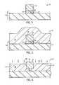
- FIG. 1is a schematic cross-sectional view of a portion of an integrated circuit in accordance with an exemplary embodiment of the present invention, the portion including a thin film transistor;
- FIG. 2is a schematic cross-sectional view of the portion of the integrated circuit illustrated in FIG. 1, showing a lithographic patterning step;
- FIG. 3is a schematic cross-sectional view of the portion of the integrated circuit illustrated in FIG. 1, showing a sacrificial gate conductor formation step;
- FIG. 4is a schematic cross-sectional view of the portion of the integrated circuit illustrated in FIG. 1, showing a photoresist stripping step;
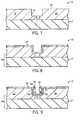
- FIG. 5is a schematic cross-sectional view of the portion of the integrated circuit illustrated in FIG. 1, showing an amorphous semiconductor deposition step;
- FIG. 6is a schematic cross-sectional view of the portion of the integrated circuit illustrated in FIG. 1, showing an anisotropic etching step and a source/drain implant step;
- FIG. 7is a schematic cross-sectional view of the portion of the integrated circuit illustrated in FIG. 1, showing a crystallization step and removal step;
- FIG. 8is a schematic cross-sectional view of the portion of the integrated circuit illustrated in FIG. 1, showing a gate dielectric deposition step
- FIG. 9is a cross-sectional view of the portion of the integrated circuit illustrated in FIG. 1, showing a spacer formation step.
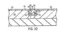
- FIG. 10is a cross-sectional view of the portion of the integrated circuit illustrated in FIG. 1, showing a gate conductor formation step.
- a portion 10 of an integrated circuitincludes a transistor 12 which is disposed on a semiconductor substrate 14 , such as, a wafer.
- Semiconductor substrate 14is preferably a semiconductor-on-insulator (SOI) substrate (e.g., a silicon-on-glass substrate).
- SOIsemiconductor-on-insulator
- substrate 14can be any type of IC substrate including gallium arsenide (GaAs), germanium, or a bulk P-type silicon substrate.
- Substrate 14preferably includes a thin or ultra-thin semiconductor layer 15 and a thick insulative layer 17 .
- Insulative layer 17can be a 500-2000 ⁇ thick silicon dioxide material.
- Semiconductor layer 15can be a 5-20 nanometer thick single crystal silicon film.
- a film or layer 15can include other semiconductor materials, such as, germanium, and can be amorphous or polycrystalline.
- layer 15is crystalline so it can act as a seed layer in a subsequent solid phase epitaxy process step.
- Transistor 12is preferably a thin film, fully-depleted (FD) SOI MOSFET having a raised source/drain structure 20 .
- Transistor 12can be formed on an island of a silicon thin film (e.g., layer 15 ).
- Raised source/drain structure 20provides more room for thick silicidation layers, such as, a silicide layer 56 .
- Silicide layer 56advantageously reduces source/drain series resistance.
- Transistor 12can be embodied as a P-channel or N-channel metal oxide semiconductor field effect transistor (MOSFET) and is described below as an N-channel transistor.
- MOSFETmetal oxide semiconductor field effect transistor
- Transistor 12includes a gate structure 18 , an elevated source region 22 , and an elevated drain region 24 .
- Regions 22 and 24extend from a top surface 21 (above a top surface 27 of substrate 14 ) to a bottom 55 in substrate 14 .
- Regions 22 and 24are 800-2000 ⁇ deep (from surface 21 to bottom 55 ).
- Regions 22 and 24can include a source extension, a drain extension, a deep source region, and a deep drain region.
- regions 22 and 24are heavily doped with N-type dopants (e.g., 5 ⁇ 10 19 -1 ⁇ 10 20 dopants per cubic centimeter).
- regions 22 and 24are heavily doped with P-type dopants (e.g., 5 ⁇ 10 19 -1 ⁇ 10 20 dopants per cubic centimeter).
- An appropriate dopant for a P-channel transistoris boron, boron diflouride, or iridium, and an appropriate dopant for an N-type transistor is arsenic, phosphorous, or antimony.
- Gate stack or structure 18includes a gate dielectric layer 34 and a gate conductor 36 . Structure 18 is disposed in an aperture 78 . Aperture 78 is preferably 800-2000 ⁇ deep and 500-2000 ⁇ wide. A channel region 41 underneath gate structure 18 separates regions 22 and 24 . Region 41 can be doped in a variety of fashions according to transistor specifications and operating parameters.
- Dielectric layer 34can be comprised of an insulative material, such as silicon dioxide or silicon nitride. Preferably, layer 34 is a 50-200 ⁇ thick layer of silicon dioxide.
- layer 34can be a 5-20 nm thick conformal layer of tantalum pentaoxide (Ta 2 O 5 ), aluminum oxide (Al 2 O 3 ), titanium dioxide (TiO 2 ), silicon nitride (SiN 3 ) or other material having a dielectric constant (k) over or at least 8.
- Ta 2 O 5tantalum pentaoxide
- Al 2 O 3aluminum oxide
- TiO 2titanium dioxide
- SiN 3silicon nitride
- kdielectric constant
- dielectric layer 34can be deposited by CVD as silicon nitride over substrate 14 .
- Layer 34is U-shaped in cross-section and has a bottom surface coplanar with top surface 27 of substrate 14 at its lowest point.
- Layer 34also includes portions 38 above regions 22 and 24 .
- Gate conductor 36is disposed above layer 34 within aperture 78 .
- Conductor 36can be 800-2000 ⁇ thick and 800-2000 ⁇ wide.
- Conductor 36is preferably a layer of conductive material.
- Gate conductor 36is preferably a metal, such as titanium nitride (TiN), tungsten (W), molybdenum (Mo), etc.
- conductor 36can be polysilicon or polysilicon/germanium.
- Gate structure 18can also include oxide liners or spacers 62 .
- Spacers 62abut sidewalls of gate conductor 36 .
- Spacers 62are disposed within aperture 78 and between layer 34 and sidewalls of conductor 36 .
- Spacers 62are preferably silicon nitride (Si 3 N 4 ) having a width of 200-500 ⁇ and a thickness (height) of 800-2000 ⁇ .
- Spacers 62can be other insulative materials, such as, silicon dioxide.
- Silicide layer 56is disposed on top of source region 22 and drain region 24 (e.g., adjacent aperture 78 ).
- layer 56is a cobalt silicide (CoSi x ).
- layer 56can be any type of refractory metal and silicon combination, such as, a nickel silicide, tungsten silicide, titanium or other silicide material.
- layer 56is 300-600 ⁇ thick.
- An insulative layercan be disposed above layer 56 . Contacts can be coupled to layer 56 through the insulative layer to connect regions 22 and 24 to conductive lines.
- the fabrication of a thin film, fully depleted transistor 12including elevated source region 22 and elevated drain region 24 , is described as follows.
- the advantageous processallows silicide layer 56 above source and drain regions 22 and 24 to be formed without adversely affecting doping characteristics of transistor 12 .
- substrate 14is embodied as an SOI substrate including a layer 15 above a layer 17 .
- Layer 15can be a 5-20 nanometer silicon film above a silicon dioxide material, such as layer 17 .
- Substrate 14can be a conventional SOI substrate available from wafer manufacturers.
- Layer 15can be doped for appropriate channel characteristics.
- a sacrificial or mask layer 19is provided above layer 15 .
- layer 19is a 100-200 nanometer thick silicon nitride layer.
- Layer 19can be deposited by chemical vapor deposition (CVD).
- a conventional lithographic stepcan be utilized to form photoresist feature 23 above layer 19 .
- Feature 23corresponds to the width of gate structure 18 or aperture 78 (FIG. 1) and can be approximately 50-300 nanometers.
- Conventional lithographycan be utilized to form feature 23 .
- layer 19is etched in accordance with feature 23 to form a sacrificial gate structure or mask structure 25 .
- Layer 19can be etched by plasma dry etching. The etching can be performed anisotropically.
- layer 15can be etched by plasma dry etching. Etching layer 15 provides a thin film semiconductor island 29 between structure 25 and layer 17 . In FIG. 4, a conventional stripping process is utilized to remove feature 23 from structure 25 .
- a semiconductor material 35is deposited above layer 17 and structure 25 .
- Semiconductor material 35can be a 2000-5000 ⁇ thick film of the same material as layer 15 (e.g., silicon).
- layer 35can be or include other semiconductor materials, such as, germanium.
- Layer 35can be deposited by low pressure CVD (LPCVD) at temperatures of less than 450° C. (e.g., 400-450° C.).
- Layer 35is utilized to form elevated source region 22 and elevated drain region 24 (FIG. 1 ).
- Layer 35is preferably an undoped amorphous material, such as, amorphous silicon.
- layer 35can be an in-situ doped semiconductor material.
- layer 35is planarized by, for example, a chemical mechanical polish (CMP).
- CMPchemical mechanical polish
- the CMP stepremoves layer 35 to expose mask structure 25 (e.g., layer 19 above island 29 ).
- a removal processis utilized so that a top surface 53 of layer 35 is lower than a top surface 55 of mask structure 25 .
- a CMP processis utilized to expose structure 25 or a separate etching technique can be utilized to lower layer 35 .
- the lowering of layer 35prevents bridging during subsequent silicidation steps described below with reference to FIG. 1 .
- layer 35is subject to a source/drain implant.
- N-type or P-type dopantsare provided by ion implantation to a depth of 300-800 ⁇ below surface 53 .
- the dopantscan be implanted in a conventional ion implantation technique utilizing implantation devices manufactured by companies, such as, Varion Company of Palo Alto, Calif., Genius Company, and Applied Materials, Inc.
- the dopantsare implanted as ions at 10-100 keV at a dose of 1 ⁇ 10 15 -6 ⁇ 10 .. dopants per square centimeter.
- Channel region 41is protected by mask structure 25 during the dopant implant.
- Layer 35is doped utilizing non-neutral dopants, such as, phosphorous (P), boron (B), arsenic (As), antimony (Sb), indium (In), or gallium (Ga).
- non-neutral dopantssuch as, phosphorous (P), boron (B), arsenic (As), antimony (Sb), indium (In), or gallium (Ga).
- layer 35is crystallized.
- layer 35is crystallized to form a single crystal material, such as, single crystal silicon.
- Layer 35can be crystallized in an annealing process to change the structure of layer 35 from an amorphous state to a single crystalline state (e.g., by melting layer 35 which subsequently recrystallizes).
- a solid phase epitaxy techniqueis utilized to crystallize layer 35 . Recrystallization of layer 35 provides an elevated source region 22 and drain region 24 .
- Gate structure 18(see FIG. 1) is advantageously self-aligned to source region 22 and drain region 24 .
- Solid phase epitaxyrefers to a crystallization process by which an amorphous semiconductor film (silicon, silicon/germanium, or germanium) is converted into crystalline semiconductor (silicon, silicon/germanium, or germanium) of a single orientation matching the orientation of an existing crystalline semiconductor (silicon, silicon/germanium, or germanium) start layer.
- amorphous semiconductor filmsilicon, silicon/germanium, or germanium
- crystalline semiconductorsilicon, silicon/germanium, or germanium
- FIG. 6sidewalls 36 (FIG. 5) of feature 29 of layer 15 provide the start layer for recrystallization.
- Solid phase epitaxyis usually achieved by heating the amorphous semiconductor.
- a low temperature (e.g., 600-650° C.) thermal annealis utilized.
- a rapid thermal anneal (RTA) or a laser annealcan be utilized.
- the annealing processis an excimer laser process (e.g., 308 nm wavelength) for a pulse duration of several nanoseconds.
- the annealing technique using an excimer lasercan raise the temperature of layer 35 to the melting temperature of layer 35 (1100° C.) for silicon or germanium.
- the melting temperature of layer 35 in the amorphous stateis significantly lower than that of layer 15 , which is in the crystalline state.
- the melting temperature of amorphous siliconis 1100° C.
- the melting temperature of a single crystal silicon substrate, such as, layer 15 (e.g., C—Si)is 1400° C.
- the annealing processis controlled so that layer 35 is fully melted and layer 15 is not melted. After the energy associated with the annealing process is removed, layer 35 is recrystallized as a single crystal material.
- feature 25(e.g., layer 25 ) is removed from portion 10 to leave an aperture 78 defined by layer 53 , source region 22 , drain region 24 and channel region 41 .
- Aperture 78is preferably 50-300 nanometers thick (e.g., the same thickness as feature 25 ).
- Feature 25can be removed in a wet chemical etch process. Alternatively, removal processes including dry etching, plasma dry etching, etc., can be utilized depending on materials associated with portion 10 .
- dielectric layer 34is deposited in aperture 78 and on top surface 53 of layer 35 .
- Layer 34prevents bridging between layer 56 and gate conductor 36 (FIG. 1 ).
- Layer 34can be conformally deposited as a 50-200 ⁇ thick silicon nitride layer by CVD.
- layer 34can be a high-k gate dielectric formed according to the process of U.S. Pat. No. 6,100,120.
- layer 34can be deposited as a metal and thereafter oxidized to form layer 34 .
- layer 34can be deposited by sputtering or by metal organic CVD.
- portion 10is subjected to a spacer formation process which creates spacers 62 on sidewalls 92 of dielectric layer 34 .
- Dielectric layer 34defines an aperture 80 .
- spacers 62are narrow and are formed in a low temperature process.
- Spacers 62are preferably 100-1000 ⁇ wide (e.g., left to right) and 500-2000 ⁇ thick (e.g., top (from a top surface of layer 34 ) to bottom (to top surface 37 )).
- Spacers 62are silicon nitride and are formed in a conventional deposition and etch-back process.
- gate conductor 36is provided between spacers 62 .
- Gate conductor 36is preferably 200-2000 ⁇ wide and 500-2000 ⁇ high.
- Gate conductor 36can be a metal gate electrode or other conductive material.
- gate conductor 36can be a titanium nitride material, tungsten material, molybdenum material, aluminum material, or other metal.
- gate conductor 36can be a doped polysilicon material or other semiconductive material.
- Conductor 36is preferably provided between spacers 62 by a conformal deposition followed by an etch or polish.
- layer 56is formed above regions 22 and 24 .
- Layer 56can be formed in a self-aligned silicide process.
- the processis preferably a cobalt silicide process having an anneal temperature of 800-825° C.
- Layer 34is removed from surface 53 of layer 35 .
- Layer 34is removed from above regions 22 and 24 to allow electrical contact to regions 22 and 24 .
- Layer 34can be selectively removed in a lithographic process by dry etching.
- layer 56is formed above regions 22 and 24 .
- a layer of cobaltis deposited by sputter deposition over regions 22 and 24 . After deposition, the layer of cobalt is heated to react with substrate 14 and form layer 56 .
- Layer 56is preferably 100-500 ⁇ thick and consumes 30 percent of its thickness from substrate 14 . High temperature processes can be utilized for layer 56 because dielectric layer 34 has not yet been formed.
- layer 56can be a titanium silicide, nickel silicide, tungsten silicide or other material.
- an insulative layercan be provided above layer 56 in a tetraethylorthosilicate TEOS deposition process. After the insulative layer is deposited and planarized, vias for contacts can be etched. Contacts can be provided to connect layers 56 to conductive lines. Conventional integrated circuit fabrication processes can be utilized to provide various other connections and form other devices as necessary for portion 10 of the integrated circuit.
Landscapes
- Thin Film Transistor (AREA)
Abstract
Description
CROSS-REFERENCE TO RELATED APPLICATIONS
This patent application is related to U.S. application Ser. No. 09/405,831, now issued U.S. Pat. No. 6,248,637, filed on Sep. 24, 1999, by Yu, entitled “A Process for Manufacturing MOS Transistors Having Elevated Source and Drain Regions,” U.S. application Ser. No. 09/397,217, filed on Sep. 16, 1999, by Yu et al., now issued U.S. Pat. No. 6,403,433, entitled “Source/Drain Doping Technique for Ultra-Thin-Body SOI MOS Transistors,” and U.S. application Ser. No. 09/384,121, filed on Aug. 27, 1999, by Yu, now issued U.S. Pat. No. 6,265,293, entitled “CMOS Transistors Fabricated in Optimized RTA Scheme.” This patent application is also related to U.S. application Ser. No. 09/609,613, filed on Jul. 5, 2000 herewith by Yu entitled, now issued U.S. Pat. No. 6,399,450, “A Process for Manufacturing MOS Transistors having Elevated Source and Drain Regions”. This patent application is also related to U.S. Pat. application Ser. No. 09/781,039, filed on an even date herewith by Yu, entitled “Low Temperature Process to Locally Form High-K Gate Dielectrics,” U.S. Pat. application Ser. No. 09/779,985, filed on an even date herewith by Yu, entitled “Replacement Gate Process for Transistor Having Elevated Source and Drain,” U.S. Pat. application Ser. No. 09/779,986, filed on an even date herewith by Yu, entitled “A Low Temperature Process For a Thin Film Transistor,” U.S. Pat. application Ser. No. 09/779,988, filed on an even date herewith by Yu, entitled “Low Temperature Process for Transistors with Elevated Source and Drain,” and U.S. Pat. application Ser. No. 09/779,987, now issued U.S. Pat. No. 6,403,434, filed on an even date herewith by Yu, entitled “A Process for Manufacturing MOS Transistors Having Elevated Source and Drain Regions and a High-K Gate Dielectric.” All of the above patent applications are assigned to the assignee of the present application.
This patent application is related to U.S. application Ser. No. 09/405,831, now issued U.S. Pat. No. 6,248,637, filed on Sep. 24, 1999, by Yu, entitled “A Process for Manufacturing MOS Transistors Having Elevated Source and Drain Regions,” U.S. application Ser. No. 09/397,217, filed on Sep. 16, 1999, by Yu et al., now issued U.S. Pat. No. 6,403,433, entitled “Source/Drain Doping Technique for Ultra-Thin-Body SOI MOS Transistors,” and U.S. application Ser. No. 09/384,121, filed on Aug. 27, 1999, by Yu, now issued U.S. Pat. No. 6,265,293, entitled “CMOS Transistors Fabricated in Optimized RTA Scheme.” This patent application is also related to U.S. application Ser. No. 09/609,613, filed on Jul. 5, 2000 herewith by Yu entitled, now issued U.S. Pat. No. 6,399,450, “A Process for Manufacturing MOS Transistors having Elevated Source and Drain Regions”. This patent application is also related to U.S. Pat. application Ser. No. 09/781,039, filed on an even date herewith by Yu, entitled “Low Temperature Process to Locally Form High-K Gate Dielectrics,” U.S. Pat. application Ser. No. 09/779,985, filed on an even date herewith by Yu, entitled “Replacement Gate Process for Transistor Having Elevated Source and Drain,” U.S. Pat. application Ser. No. 09/779,986, filed on an even date herewith by Yu, entitled “A Low Temperature Process For a Thin Film Transistor,” U.S. Pat. application Ser. No. 09/779,988, filed on an even date herewith by Yu, entitled “Low Temperature Process for Transistors with Elevated Source and Drain,” and U.S. Pat. application Ser. No. 09/779,987, now issued U.S. Pat. No. 6,403,434, filed on an even date herewith by Yu, entitled “A Process for Manufacturing MOS Transistors Having Elevated Source and Drain Regions and a High-K Gate Dielectric.” All of the above patent applications are assigned to the assignee of the present application.
The present specification relates to integrated circuits (ICs) and methods of manufacturing integrated circuits. More particularly, the present application relates to a method of manufacturing integrated circuits having thin film transistors.
Currently, deep-submicron complementary metal oxide semiconductor (CMOS) is the primary technology for ultra-large scale integrated (ULSI) devices. Over the last two decades, reducing the size of CMOS transistors and increasing transistor density on ICs has been a principal focus of the microelectronics industry. An ultra-large scale integrated circuit can include over 1 million transistors. Transistors, such as, metal oxide semiconductor field effect transistors (MOSFETs), are generally bulk semiconductor-type devices or silicon-on-insulator (SOI)-type devices.
In bulk semiconductor-type devices, transistors, such as, MOSFETs are built on the top surface of a bulk substrate. The substrate is doped to form source and drain regions, and a conductive layer is provided on the top surface between the source and drain regions. The conductive layer operates as a gate for the transistor; the gate controls current in a channel between the source and the drain regions. As transistors become smaller, the body thickness of the transistor (and thickness of the depletion layer below the inversion channel) must be scaled down to achieve superior short channel performance.
According to conventional complimentary metal oxide semiconductor (CMOS) fabrication techniques, the reduction of the depletion layer thickness is realized by a super-steep retrograded well (SSRW) ion implantation process. However, this process is limited by the diffusion of dopant atoms during subsequent thermal processes (e.g., annealing). The ion implantation process can generally only achieve an 80-nanometer or larger body thickness for a transistor. Thus, conventional fabrication techniques for bulk semiconductor type-devices cannot create transistors with a body thickness less than 80 nm.
Accordingly, bulk semiconductor-type devices can be subject to disadvantageous properties due to the relatively large body thicknesses. These disadvantageous properties include less than ideal sub-threshold voltage rolloff, short channel effects, and drain induced barrier lowering. Further still, bulk semiconductor-type devices can be subject to further disadvantageous properties such as high junction capacitance, ineffective isolation, and low saturation current. These properties are accentuated as transistors become smaller and transistor density increases on ICs.
The ULSI circuit can include CMOS field effect transistors (FETS) which have semiconductor gates disposed between drain and source regions. The drain and source regions are typically heavily doped with a P-type dopant (boron) or an N-type dopant (phosphorous).
The source and drain regions are often silicided to reduce source/drain series resistance or contact resistance. However, as body thickness is reduced, the amount of material available for silicidation is reduced. Accordingly, large source/drain series resistance remains a considerable factor adversely affecting device performance.
The source and drain regions can be raised by selective silicon (Si) epitaxy to make connections to source and drain contacts less difficult. The raised source and drain regions provide additional material for contact silicidation processes and thereby reduce deep source/drain junction resistance and source/drain series resistance. However, the epitaxy process that forms the raised source and drain regions generally requires high temperatures exceeding 1000° C. (e.g., 1100-1200° C.). These high temperatures increase the thermal budget of the process and can adversely affect the formation of steep retrograde well regions and ultra shallow source/drain extensions.
The high temperatures, often referred to as a high thermal budget, can produce significant thermal diffusion which can cause shorts between the source and drain region (between the source/drain extensions). The potential for shorting between the source and drain region increases as gate lengths decrease.
Conventional SOI-type devices include an insulative substrate attached to a thin film semiconductor substrate which contains transistors similar to the MOSFET described with respect to bulk semiconductor-type devices. The transistors have superior performance characteristics due to the thin film nature of the semiconductor substrate and the insulative properties of the insulative substrate (e.g., the floating body effect). The superior performance is manifested in superior short channel performance (i.e., resistance to process variation in small size transistor), near-ideal subthreshold voltage swing (i.e., good for low off-state current leakage), and high saturation current.
As transistors become smaller, the thin film semiconductor substrate also becomes thinner. The thinness of the thin film semiconductor substrate prevents effective silicidation on the thin film semiconductor substrate. Effective silicidation is necessary to form source and drain contacts. Without effective silicidation, the transistor can have large source/drain series resistances.
Typically, silicidation must consume a certain volume of the semiconductor substrate (e.g., silicon), which is not abundantly available on the thin film semiconductor substrate. The significant volume of the substrate must be consumed to appropriately make electrical contact to the source and drain regions. Accordingly, SOI-type devices are susceptible to the high series source/drain resistance which can degrade transistor saturation current and hence, the speed of the transistor. The high series resistance associated with conventional SOI CMOS technology is a major obstacle which prevents SOI technology from becoming a mainstream IC technology.
Thus, there is a need for a method of manufacturing thin film, fully depleted MOSFET ICs which has advantages over conventional bulk type devices. Further still, there is a need for a method of manufacturing a transistor which has superior short-channel performance, near ideal subthreshold swing, and high saturation current and yet is not susceptible to high series resistance and tunnel leakage current. Even further still, there is a need for a process for making a thin film transistor which has sufficient silicon for effective silicidation and includes a high-k gate dielectric. Yet further, there is a need for a fully depleted, thin film transistor with elevated source and drain regions and high-k gate dielectrics manufactured in an optimized annealing process. Yet even further, there is a need for a process flow of forming elevated source and drain regions on an SOI-substrate before forming a high-k gate dielectric.
An exemplary embodiment relates to a method of manufacturing an integrated circuit. The integrated circuit includes a thin film transistor on a substrate. A substrate includes a thin semiconductor layer. The method includes steps of providing a sacrificial gate structure on the thin film semiconductor layer of the substrate, etching the substrate in accordance with the sacrificial gate structure, providing an amorphous semiconductor layer above the substrate and over the gate structure, removing a portion of the amorphous semiconductor layer to expose the gate structure, and forming a single crystalline material from the amorphous semiconductor material. The method also includes steps of siliciding the single crystalline material, removing the sacrificial gate structure to form an aperture, and providing a gate conductor in the aperture.
Another exemplary embodiment relates to a method of manufacturing an ultra-large scale integrated circuit including a transistor. The method includes providing a mask structure on a top surface of a thin film, depositing a semiconductor material above the top surface of the thin film and the mask structure, removing the semiconductor material to a level below a top surface of the mask structure, siliciding the semiconductor material, removing the mask structure to leave an aperture, and providing a gate conductor in the aperture.
Yet another exemplary embodiment relates to a transistor including a thin film, a gate structure, source and drain regions, and a silicide layer. The gate structure includes a gate dielectric above the thin film and a gate conductor above a portion of the gate dielectric. The source and drain regions are adjacent to the gate structure. The silicide layer has a top surface above a bottom surface of the gate conductor and below a top surface of the gate conductor. The gate dielectric is at least partially above the top surface of the silicide layer.
Exemplary embodiments will hereafter be described with reference to the accompanying drawings, wherein like numerals denote like elements, and:
FIG. 1 is a schematic cross-sectional view of a portion of an integrated circuit in accordance with an exemplary embodiment of the present invention, the portion including a thin film transistor;
FIG. 2 is a schematic cross-sectional view of the portion of the integrated circuit illustrated in FIG. 1, showing a lithographic patterning step;
FIG. 3 is a schematic cross-sectional view of the portion of the integrated circuit illustrated in FIG. 1, showing a sacrificial gate conductor formation step;
FIG. 4 is a schematic cross-sectional view of the portion of the integrated circuit illustrated in FIG. 1, showing a photoresist stripping step;
FIG. 5 is a schematic cross-sectional view of the portion of the integrated circuit illustrated in FIG. 1, showing an amorphous semiconductor deposition step;
FIG. 6 is a schematic cross-sectional view of the portion of the integrated circuit illustrated in FIG. 1, showing an anisotropic etching step and a source/drain implant step;
FIG. 7 is a schematic cross-sectional view of the portion of the integrated circuit illustrated in FIG. 1, showing a crystallization step and removal step;
FIG. 8 is a schematic cross-sectional view of the portion of the integrated circuit illustrated in FIG. 1, showing a gate dielectric deposition step;
FIG. 9 is a cross-sectional view of the portion of the integrated circuit illustrated in FIG. 1, showing a spacer formation step; and
FIG. 10 is a cross-sectional view of the portion of the integrated circuit illustrated in FIG. 1, showing a gate conductor formation step.
With reference to FIG. 1, aportion 10 of an integrated circuit (IC) includes atransistor 12 which is disposed on asemiconductor substrate 14, such as, a wafer.Semiconductor substrate 14 is preferably a semiconductor-on-insulator (SOI) substrate (e.g., a silicon-on-glass substrate). Alternatively,substrate 14 can be any type of IC substrate including gallium arsenide (GaAs), germanium, or a bulk P-type silicon substrate.
Gate stack orstructure 18 includes agate dielectric layer 34 and agate conductor 36.Structure 18 is disposed in anaperture 78.Aperture 78 is preferably 800-2000 Å deep and 500-2000 Å wide. Achannel region 41 underneathgate structure 18separates regions Region 41 can be doped in a variety of fashions according to transistor specifications and operating parameters.
Alternatively,layer 34 can be a 5-20 nm thick conformal layer of tantalum pentaoxide (Ta2O5), aluminum oxide (Al2O3), titanium dioxide (TiO2), silicon nitride (SiN3) or other material having a dielectric constant (k) over or at least 8.
In a preferred embodiment,dielectric layer 34 can be deposited by CVD as silicon nitride oversubstrate 14.Layer 34 is U-shaped in cross-section and has a bottom surface coplanar withtop surface 27 ofsubstrate 14 at its lowest point.Layer 34 also includesportions 38 aboveregions
An insulative layer can be disposed abovelayer 56. Contacts can be coupled tolayer 56 through the insulative layer to connectregions
With reference to FIGS. 1-10, the fabrication of a thin film, fully depletedtransistor 12, includingelevated source region 22 andelevated drain region 24, is described as follows. The advantageous process allowssilicide layer 56 above source and drainregions transistor 12.
With reference to FIG. 2,substrate 14 is embodied as an SOI substrate including alayer 15 above alayer 17.Layer 15 can be a 5-20 nanometer silicon film above a silicon dioxide material, such aslayer 17.Substrate 14 can be a conventional SOI substrate available from wafer manufacturers.Layer 15 can be doped for appropriate channel characteristics.
A sacrificial ormask layer 19 is provided abovelayer 15. Preferably,layer 19 is a 100-200 nanometer thick silicon nitride layer.Layer 19 can be deposited by chemical vapor deposition (CVD). A conventional lithographic step can be utilized to formphotoresist feature 23 abovelayer 19.Feature 23 corresponds to the width ofgate structure 18 or aperture78 (FIG. 1) and can be approximately 50-300 nanometers. Conventional lithography can be utilized to formfeature 23.
In FIG. 3,layer 19 is etched in accordance withfeature 23 to form a sacrificial gate structure ormask structure 25.Layer 19 can be etched by plasma dry etching. The etching can be performed anisotropically.
After etchinglayer 19,layer 15 can be etched by plasma dry etching.Etching layer 15 provides a thinfilm semiconductor island 29 betweenstructure 25 andlayer 17. In FIG. 4, a conventional stripping process is utilized to removefeature 23 fromstructure 25.
In FIG. 5, asemiconductor material 35 is deposited abovelayer 17 andstructure 25.Semiconductor material 35 can be a 2000-5000 Å thick film of the same material as layer15 (e.g., silicon). Alternatively,layer 35 can be or include other semiconductor materials, such as, germanium.Layer 35 can be deposited by low pressure CVD (LPCVD) at temperatures of less than 450° C. (e.g., 400-450° C.).
In FIG. 6, afterlayer 35 is deposited,layer 35 is planarized by, for example, a chemical mechanical polish (CMP). The CMP step removeslayer 35 to expose mask structure25 (e.g.,layer 19 above island29). Aftermask structure 25 is exposed, a removal process is utilized so that atop surface 53 oflayer 35 is lower than atop surface 55 ofmask structure 25. A CMP process is utilized to exposestructure 25 or a separate etching technique can be utilized tolower layer 35. The lowering oflayer 35 prevents bridging during subsequent silicidation steps described below with reference to FIG.1.
Afterlayer 35 is polished,layer 35 is subject to a source/drain implant. Preferably, N-type or P-type dopants are provided by ion implantation to a depth of 300-800 Å belowsurface 53. The dopants can be implanted in a conventional ion implantation technique utilizing implantation devices manufactured by companies, such as, Varion Company of Palo Alto, Calif., Genius Company, and Applied Materials, Inc. Preferably, the dopants are implanted as ions at 10-100 keV at a dose of 1×10¹⁵-6×10‥dopants per square centimeter.
After dopants are implanted intolayer 35,layer 35 is crystallized. Preferably,layer 35 is crystallized to form a single crystal material, such as, single crystal silicon.Layer 35 can be crystallized in an annealing process to change the structure oflayer 35 from an amorphous state to a single crystalline state (e.g., by meltinglayer 35 which subsequently recrystallizes). Preferably, a solid phase epitaxy technique is utilized to crystallizelayer 35. Recrystallization oflayer 35 provides anelevated source region 22 and drainregion 24. Gate structure18 (see FIG. 1) is advantageously self-aligned to sourceregion 22 and drainregion 24.
Solid phase epitaxy refers to a crystallization process by which an amorphous semiconductor film (silicon, silicon/germanium, or germanium) is converted into crystalline semiconductor (silicon, silicon/germanium, or germanium) of a single orientation matching the orientation of an existing crystalline semiconductor (silicon, silicon/germanium, or germanium) start layer. In FIG. 6, sidewalls36 (FIG. 5) offeature 29 oflayer 15 provide the start layer for recrystallization.
Solid phase epitaxy is usually achieved by heating the amorphous semiconductor. Preferably, a low temperature (e.g., 600-650° C.) thermal anneal is utilized. Alternatively, a rapid thermal anneal (RTA) or a laser anneal can be utilized.
In one embodiment, the annealing process is an excimer laser process (e.g., 308 nm wavelength) for a pulse duration of several nanoseconds. The annealing technique using an excimer laser can raise the temperature oflayer 35 to the melting temperature of layer35 (1100° C.) for silicon or germanium. The melting temperature oflayer 35 in the amorphous state is significantly lower than that oflayer 15, which is in the crystalline state. For example, the melting temperature of amorphous silicon is 1100° C., and the melting temperature of a single crystal silicon substrate, such as, layer15 (e.g., C—Si) is 1400° C. Preferably, the annealing process is controlled so thatlayer 35 is fully melted andlayer 15 is not melted. After the energy associated with the annealing process is removed,layer 35 is recrystallized as a single crystal material.
With reference to FIG. 7, feature25 (e.g., layer25) is removed fromportion 10 to leave anaperture 78 defined bylayer 53,source region 22,drain region 24 andchannel region 41.Aperture 78 is preferably 50-300 nanometers thick (e.g., the same thickness as feature25).Feature 25 can be removed in a wet chemical etch process. Alternatively, removal processes including dry etching, plasma dry etching, etc., can be utilized depending on materials associated withportion 10.
Afteraperture 78 is formed,dielectric layer 34 is deposited inaperture 78 and ontop surface 53 oflayer 35.Layer 34 prevents bridging betweenlayer 56 and gate conductor36 (FIG.1).Layer 34 can be conformally deposited as a 50-200 Å thick silicon nitride layer by CVD.
Alternatively,layer 34 can be a high-k gate dielectric formed according to the process of U.S. Pat. No. 6,100,120. For example,layer 34 can be deposited as a metal and thereafter oxidized to formlayer 34. In another alternative,layer 34 can be deposited by sputtering or by metal organic CVD.
In FIG. 9,portion 10 is subjected to a spacer formation process which creates spacers62 onsidewalls 92 ofdielectric layer 34.Dielectric layer 34 defines anaperture 80. Preferably, spacers62 are narrow and are formed in a low temperature process.Spacers 62 are preferably 100-1000 Å wide (e.g., left to right) and 500-2000 Å thick (e.g., top (from a top surface of layer34) to bottom (to top surface37)).Spacers 62 are silicon nitride and are formed in a conventional deposition and etch-back process.
In FIG. 10, after spacers62 are formed,gate conductor 36 is provided betweenspacers 62.Gate conductor 36 is preferably 200-2000 Å wide and 500-2000 Å high.Gate conductor 36 can be a metal gate electrode or other conductive material. For example,gate conductor 36 can be a titanium nitride material, tungsten material, molybdenum material, aluminum material, or other metal. Alternatively,gate conductor 36 can be a doped polysilicon material or other semiconductive material.Conductor 36 is preferably provided betweenspacers 62 by a conformal deposition followed by an etch or polish.
In FIG. 1,layer 56 is formed aboveregions Layer 56 can be formed in a self-aligned silicide process. The process is preferably a cobalt silicide process having an anneal temperature of 800-825°C. Layer 34 is removed fromsurface 53 oflayer 35.Layer 34 is removed from aboveregions regions Layer 34 can be selectively removed in a lithographic process by dry etching.
Afterlayer 34 is removed,layer 56 is formed aboveregions regions substrate 14 andform layer 56.Layer 56 is preferably 100-500 Å thick and consumes 30 percent of its thickness fromsubstrate 14. High temperature processes can be utilized forlayer 56 becausedielectric layer 34 has not yet been formed. Alternatively,layer 56 can be a titanium silicide, nickel silicide, tungsten silicide or other material.
Afterlayer 56 is formed, an insulative layer can be provided abovelayer 56 in a tetraethylorthosilicate TEOS deposition process. After the insulative layer is deposited and planarized, vias for contacts can be etched. Contacts can be provided to connectlayers 56 to conductive lines. Conventional integrated circuit fabrication processes can be utilized to provide various other connections and form other devices as necessary forportion 10 of the integrated circuit.
It is understood that while the detailed drawings, specific examples, material types, thicknesses, dimensions, and particular values given provide a preferred exemplary embodiment of the present invention, the preferred exemplary embodiment is for the purpose of illustration only. The method and apparatus of the invention is not limited to the precise details and conditions disclosed. For example, although specific types of structures are shown, other structures can be utilized. Various changes may be made to the details disclosed without departing from the scope of the invention which is defined by the following claims.
Claims (20)
1. A method of manufacturing an integrated circuit, the integrated circuit including a thin film transistor on a substrate, the substrate including a thin semiconductor layer, the method comprising steps of:
providing a sacrificial gate structure on the thin semiconductor layer of the substrate;
etching the thin semiconductor layer in accordance with the sacrificial gate structure;
providing an amorphous semiconductor layer above the substrate and over the gate structure;
removing a portion of the amorphous semiconductor layer to expose the sacrificial gate structure;
forming a single crystalline semiconductor material from the amorphous semiconductor material;
siliciding the single crystalline material;
removing the sacrificial gate structure to form an aperture; and
providing a gate conductor in the aperture.
2. The method ofclaim 1 , further comprising:
providing a spacer in the aperture before providing the gate conductor.
3. The method ofclaim 2 , further comprising:
providing a gate dielectric in the aperture before providing the spacer and above the amorphous semiconductor layer.
4. The method ofclaim 3 , wherein the siliciding step is a colbalt silicide process.
5. The method ofclaim 1 , wherein the sacrificial gate structure includes silicon nitride.
6. The method ofclaim 1 , wherein the amorphous semiconductor layer is an in-situ doped layer.
7. The method ofclaim 6 , wherein the amorphous semiconductor material includes silicon.
8. The method ofclaim 1 , wherein the substrate includes single crystalline silicon.
9. The method ofclaim 1 , wherein the amorphous semiconductor layer includes silicon germanium.
10. A method of manufacturing an ultra-large scale integrated circuit including a transistor, the method comprising:
providing a gate mask structure on a top surface of a thin film, the thin film being above a base layer;
etching the thin film in accordance with the gate mask structure;
depositing an amorphous semiconductor material above a top surface of the base layer and the mask structure;
a removing the semiconductor material to a level below a top surface of the mask structure;
crystalizing the amorphous semiconductor material;
siliciding the semiconductor material;
removing the mask structure to leave an aperture; and
providing a gate conductor in the aperture.
11. The method ofclaim 10 , further comprising:
providing an insulative layer over the silicided semiconductor material before the gate structure is provided.
12. The method ofclaim 11 , further comprising:
providing a source and drain dopant implant before the insulative layer is provided.
13. The method ofclaim 12 , further comprising: providing a high-k gate dielectric in the aperture.
14. The method ofclaim 13 , wherein the siliciding is performed at a temperature of more than 800° C.
15. The method ofclaim 11 , wherein the insulative layer has a top surface co-planer with a top surface of the mask structure.
16. The method ofclaim 10 , wherein the mask structure is a sacrificial nitride gate structure.
17. A process of manufacturing transistor including a thin film, a gate structure having a gate dielectric above the thin film and a gate conductor above a portion of the gate dielectric, source and drain regions adjacent the gate structure, and a silicide layer having a top surface above a bottom surface of the gate conductor and below a top surface of the gate conductor, the gate dielectric being at least partially above the top surface of the suicide layer, the process comprising:
providing a mask structure on a top surface of the thin film, the thin film being above a base layer;
etching the thin film in accordance with the mask structure;
depositing an amorphous semiconductor material above the top surface of the base layer and the mask structure;
removing the amorphous semiconductor material to a level below a top surface of the mask structure;
crystalizing the amorphous semiconductor material;
siliciding the crystallized semiconductor material to form the silicide layer;
removing the mask structure to leave an aperture; and
providing the gate conductor in the aperture.
18. The process ofclaim 17 , wherein the gate dielectric is U-shaped.
19. The process ofclaim 17 , wherein the gate structure includes spacers.
20. The process ofclaim 19 , wherein the spacers are disposed between a portion of the gate dielectric and the silicide layer.
Priority Applications (1)
| Application Number | Priority Date | Filing Date | Title |
|---|---|---|---|
| US09/780,043US6787424B1 (en) | 2001-02-09 | 2001-02-09 | Fully depleted SOI transistor with elevated source and drain |
Applications Claiming Priority (1)
| Application Number | Priority Date | Filing Date | Title |
|---|---|---|---|
| US09/780,043US6787424B1 (en) | 2001-02-09 | 2001-02-09 | Fully depleted SOI transistor with elevated source and drain |
Publications (1)
| Publication Number | Publication Date |
|---|---|
| US6787424B1true US6787424B1 (en) | 2004-09-07 |
Family
ID=32928120
Family Applications (1)
| Application Number | Title | Priority Date | Filing Date |
|---|---|---|---|
| US09/780,043Expired - LifetimeUS6787424B1 (en) | 2001-02-09 | 2001-02-09 | Fully depleted SOI transistor with elevated source and drain |
Country Status (1)
| Country | Link |
|---|---|
| US (1) | US6787424B1 (en) |
Cited By (68)
| Publication number | Priority date | Publication date | Assignee | Title |
|---|---|---|---|---|
| US20040021691A1 (en)* | 2000-10-18 | 2004-02-05 | Mark Dostie | Method, system and media for entering data in a personal computing device |
| DE102004044444A1 (en)* | 2004-09-14 | 2006-03-16 | Infineon Technologies Ag | Field-effect transistor semiconductor device production involves forming structured trench sidewalls |
| US20060105529A1 (en)* | 2004-11-15 | 2006-05-18 | Sang-Hyeon Lee | Methods of forming MOS transistors having buried gate electrodes therein |
| US20060194399A1 (en)* | 2004-01-08 | 2006-08-31 | Taiwan Semiconductor Manufacturing Company, Ltd. | Silicide Gate Transistors and Method of Manufacture |
| US20060228844A1 (en)* | 2005-03-30 | 2006-10-12 | Marcus Culmsee | Integration scheme for fully silicided gate |
| US20070063287A1 (en)* | 2005-09-16 | 2007-03-22 | Renesas Technology Corp. | Semiconductor device |
| US20090045458A1 (en)* | 2007-08-15 | 2009-02-19 | Advanced Micro Devices, Inc. | Mos transistors for thin soi integration and methods for fabricating the same |
| US20090148986A1 (en)* | 2007-12-06 | 2009-06-11 | International Business Machines Corporation | Method of making a finfet device structure having dual metal and high-k gates |
| US20090261391A1 (en)* | 2005-06-21 | 2009-10-22 | Jack Kavalieros | Complementary Metal Oxide Semiconductor Integrated Circuit Using Raised Source Drain and Replacement Metal Gate |
| US20100019358A1 (en)* | 2008-07-23 | 2010-01-28 | International Business Machines Corporation | Semiconductor device and method of manufacturing |
| US20100237410A1 (en)* | 2009-03-19 | 2010-09-23 | International Business Machines Corporation | Ultra-thin semiconductor on insulator metal gate complementary field effect transistor with metal gate and method of forming thereof |
| US20100301417A1 (en)* | 2009-05-26 | 2010-12-02 | International Business Machines Corporation | Device including high-k metal gate finfet and resistive structure and method of forming thereof |
| US20110062520A1 (en)* | 2005-06-15 | 2011-03-17 | Brask Justin K | Method for fabricating transistor with thinned channel |
| US8273617B2 (en) | 2009-09-30 | 2012-09-25 | Suvolta, Inc. | Electronic devices and systems, and methods for making and using the same |
| US8377783B2 (en) | 2010-09-30 | 2013-02-19 | Suvolta, Inc. | Method for reducing punch-through in a transistor device |
| US8400219B2 (en) | 2011-03-24 | 2013-03-19 | Suvolta, Inc. | Analog circuits having improved transistors, and methods therefor |
| US8404551B2 (en) | 2010-12-03 | 2013-03-26 | Suvolta, Inc. | Source/drain extension control for advanced transistors |
| US8421162B2 (en) | 2009-09-30 | 2013-04-16 | Suvolta, Inc. | Advanced transistors with punch through suppression |
| US8461875B1 (en) | 2011-02-18 | 2013-06-11 | Suvolta, Inc. | Digital circuits having improved transistors, and methods therefor |
| US8525271B2 (en) | 2011-03-03 | 2013-09-03 | Suvolta, Inc. | Semiconductor structure with improved channel stack and method for fabrication thereof |
| US8530286B2 (en) | 2010-04-12 | 2013-09-10 | Suvolta, Inc. | Low power semiconductor transistor structure and method of fabrication thereof |
| US8569156B1 (en) | 2011-05-16 | 2013-10-29 | Suvolta, Inc. | Reducing or eliminating pre-amorphization in transistor manufacture |
| US8569128B2 (en) | 2010-06-21 | 2013-10-29 | Suvolta, Inc. | Semiconductor structure and method of fabrication thereof with mixed metal types |
| US8599623B1 (en) | 2011-12-23 | 2013-12-03 | Suvolta, Inc. | Circuits and methods for measuring circuit elements in an integrated circuit device |
| US8614128B1 (en) | 2011-08-23 | 2013-12-24 | Suvolta, Inc. | CMOS structures and processes based on selective thinning |
| US8629016B1 (en) | 2011-07-26 | 2014-01-14 | Suvolta, Inc. | Multiple transistor types formed in a common epitaxial layer by differential out-diffusion from a doped underlayer |
| US8637955B1 (en) | 2012-08-31 | 2014-01-28 | Suvolta, Inc. | Semiconductor structure with reduced junction leakage and method of fabrication thereof |
| US8645878B1 (en) | 2011-08-23 | 2014-02-04 | Suvolta, Inc. | Porting a circuit design from a first semiconductor process to a second semiconductor process |
| US8713511B1 (en) | 2011-09-16 | 2014-04-29 | Suvolta, Inc. | Tools and methods for yield-aware semiconductor manufacturing process target generation |
| US8735987B1 (en) | 2011-06-06 | 2014-05-27 | Suvolta, Inc. | CMOS gate stack structures and processes |
| US8748270B1 (en) | 2011-03-30 | 2014-06-10 | Suvolta, Inc. | Process for manufacturing an improved analog transistor |
| US8748986B1 (en) | 2011-08-05 | 2014-06-10 | Suvolta, Inc. | Electronic device with controlled threshold voltage |
| US8759872B2 (en) | 2010-06-22 | 2014-06-24 | Suvolta, Inc. | Transistor with threshold voltage set notch and method of fabrication thereof |
| US8796048B1 (en) | 2011-05-11 | 2014-08-05 | Suvolta, Inc. | Monitoring and measurement of thin film layers |
| US8811068B1 (en) | 2011-05-13 | 2014-08-19 | Suvolta, Inc. | Integrated circuit devices and methods |
| US8816754B1 (en) | 2012-11-02 | 2014-08-26 | Suvolta, Inc. | Body bias circuits and methods |
| US8819603B1 (en) | 2011-12-15 | 2014-08-26 | Suvolta, Inc. | Memory circuits and methods of making and designing the same |
| US8863064B1 (en) | 2012-03-23 | 2014-10-14 | Suvolta, Inc. | SRAM cell layout structure and devices therefrom |
| US8877619B1 (en) | 2012-01-23 | 2014-11-04 | Suvolta, Inc. | Process for manufacture of integrated circuits with different channel doping transistor architectures and devices therefrom |
| US8883600B1 (en) | 2011-12-22 | 2014-11-11 | Suvolta, Inc. | Transistor having reduced junction leakage and methods of forming thereof |
| US8895327B1 (en) | 2011-12-09 | 2014-11-25 | Suvolta, Inc. | Tipless transistors, short-tip transistors, and methods and circuits therefor |
| US8970289B1 (en) | 2012-01-23 | 2015-03-03 | Suvolta, Inc. | Circuits and devices for generating bi-directional body bias voltages, and methods therefor |
| US8976575B1 (en) | 2013-08-29 | 2015-03-10 | Suvolta, Inc. | SRAM performance monitor |
| US8995204B2 (en) | 2011-06-23 | 2015-03-31 | Suvolta, Inc. | Circuit devices and methods having adjustable transistor body bias |
| US8994415B1 (en) | 2013-03-01 | 2015-03-31 | Suvolta, Inc. | Multiple VDD clock buffer |
| US8999861B1 (en) | 2011-05-11 | 2015-04-07 | Suvolta, Inc. | Semiconductor structure with substitutional boron and method for fabrication thereof |
| US9006094B2 (en) | 2012-04-18 | 2015-04-14 | International Business Machines Corporation | Stratified gate dielectric stack for gate dielectric leakage reduction |
| US9041126B2 (en) | 2012-09-21 | 2015-05-26 | Mie Fujitsu Semiconductor Limited | Deeply depleted MOS transistors having a screening layer and methods thereof |
| US9054219B1 (en) | 2011-08-05 | 2015-06-09 | Mie Fujitsu Semiconductor Limited | Semiconductor devices having fin structures and fabrication methods thereof |
| US9070477B1 (en) | 2012-12-12 | 2015-06-30 | Mie Fujitsu Semiconductor Limited | Bit interleaved low voltage static random access memory (SRAM) and related methods |
| US9093997B1 (en) | 2012-11-15 | 2015-07-28 | Mie Fujitsu Semiconductor Limited | Slew based process and bias monitors and related methods |
| US9093550B1 (en) | 2012-01-31 | 2015-07-28 | Mie Fujitsu Semiconductor Limited | Integrated circuits having a plurality of high-K metal gate FETs with various combinations of channel foundation structure and gate stack structure and methods of making same |
| US9112057B1 (en) | 2012-09-18 | 2015-08-18 | Mie Fujitsu Semiconductor Limited | Semiconductor devices with dopant migration suppression and method of fabrication thereof |
| US9112484B1 (en) | 2012-12-20 | 2015-08-18 | Mie Fujitsu Semiconductor Limited | Integrated circuit process and bias monitors and related methods |
| US9112495B1 (en) | 2013-03-15 | 2015-08-18 | Mie Fujitsu Semiconductor Limited | Integrated circuit device body bias circuits and methods |
| US20150295066A1 (en)* | 2012-09-05 | 2015-10-15 | Commissariat A L'energie Atomique Et Aux Ene Alt | Process for producing fet transistors |
| US9236466B1 (en) | 2011-10-07 | 2016-01-12 | Mie Fujitsu Semiconductor Limited | Analog circuits having improved insulated gate transistors, and methods therefor |
| US9268885B1 (en) | 2013-02-28 | 2016-02-23 | Mie Fujitsu Semiconductor Limited | Integrated circuit device methods and models with predicted device metric variations |
| US9299801B1 (en) | 2013-03-14 | 2016-03-29 | Mie Fujitsu Semiconductor Limited | Method for fabricating a transistor device with a tuned dopant profile |
| US9299698B2 (en) | 2012-06-27 | 2016-03-29 | Mie Fujitsu Semiconductor Limited | Semiconductor structure with multiple transistors having various threshold voltages |
| US9319013B2 (en) | 2014-08-19 | 2016-04-19 | Mie Fujitsu Semiconductor Limited | Operational amplifier input offset correction with transistor threshold voltage adjustment |
| US9406567B1 (en) | 2012-02-28 | 2016-08-02 | Mie Fujitsu Semiconductor Limited | Method for fabricating multiple transistor devices on a substrate with varying threshold voltages |
| US9431068B2 (en) | 2012-10-31 | 2016-08-30 | Mie Fujitsu Semiconductor Limited | Dynamic random access memory (DRAM) with low variation transistor peripheral circuits |
| US9449967B1 (en) | 2013-03-15 | 2016-09-20 | Fujitsu Semiconductor Limited | Transistor array structure |
| US9478571B1 (en) | 2013-05-24 | 2016-10-25 | Mie Fujitsu Semiconductor Limited | Buried channel deeply depleted channel transistor |
| US9640641B2 (en) | 2015-07-15 | 2017-05-02 | International Business Machines Corporation | Silicon germanium fin channel formation |
| US9710006B2 (en) | 2014-07-25 | 2017-07-18 | Mie Fujitsu Semiconductor Limited | Power up body bias circuits and methods |
| US11101367B2 (en) | 2015-06-19 | 2021-08-24 | International Business Machines Corporation | Contact-first field-effect transistors |
Citations (99)
| Publication number | Priority date | Publication date | Assignee | Title |
|---|---|---|---|---|
| US4532695A (en) | 1982-07-02 | 1985-08-06 | The United States Of America As Represented By The Secretary Of The Air Force | Method of making self-aligned IGFET |
| US4683645A (en) | 1985-06-28 | 1987-08-04 | Northern Telecom Limited | Process of fabricating MOS devices having shallow source and drain junctions |
| US4745082A (en) | 1986-06-12 | 1988-05-17 | Ford Microelectronics, Inc. | Method of making a self-aligned MESFET using a substitutional gate with side walls |
| US4784718A (en) | 1986-02-27 | 1988-11-15 | Kabushiki Kaisha Toshiba | Method for manufacturing semiconductor device |
| US4789644A (en)* | 1985-12-23 | 1988-12-06 | Sgs Microelettronica Spa | Process for fabrication, by means of epitaxial recrystallization, of insulated-gate field-effect transistors with junctions of minimum depth |
| US4835112A (en) | 1988-03-08 | 1989-05-30 | Motorola, Inc. | CMOS salicide process using germanium implantation |
| US4954867A (en) | 1987-06-18 | 1990-09-04 | Seiko Instruments Inc. | Semiconductor device with silicon oxynitride over refractory metal gate electrode in LDD structure |
| US4998150A (en) | 1988-12-22 | 1991-03-05 | Texas Instruments Incorporated | Raised source/drain transistor |
| JPH03248433A (en) | 1990-02-26 | 1991-11-06 | Nec Corp | Manufacturing method of semiconductor device |
| US5102816A (en) | 1990-03-27 | 1992-04-07 | Sematech, Inc. | Staircase sidewall spacer for improved source/drain architecture |
| JPH04123439A (en) | 1990-09-14 | 1992-04-23 | Toshiba Corp | Manufacture of semiconductor device |
| US5108954A (en) | 1991-09-23 | 1992-04-28 | Micron Technology, Inc. | Method of reducing contact resistance at silicide/active area interfaces and semiconductor devices produced according to the method |
| US5168072A (en) | 1990-10-12 | 1992-12-01 | Texas Instruments Incorporated | Method of fabricating an high-performance insulated-gate field-effect transistor |
| US5200352A (en) | 1991-11-25 | 1993-04-06 | Motorola Inc. | Transistor having a lightly doped region and method of formation |
| JPH05160396A (en) | 1991-12-06 | 1993-06-25 | Sharp Corp | MOS field effect transistor |
| JPH05206454A (en) | 1992-01-28 | 1993-08-13 | Fujitsu Ltd | Manufacture of mis-type semiconductor device |
| US5258637A (en) | 1991-09-23 | 1993-11-02 | Micron Technology, Inc. | Semiconductor devices produced according to a method which reduces contact resistance at silicide/active area interfaces |
| US5264382A (en) | 1990-03-20 | 1993-11-23 | Fujitsu Limited | Method of producing semiconductor device using dummy gate structure |
| US5320974A (en) | 1991-07-25 | 1994-06-14 | Matsushita Electric Industrial Co., Ltd. | Method for making semiconductor transistor device by implanting punch through stoppers |
| US5374575A (en) | 1993-11-23 | 1994-12-20 | Goldstar Electron Co., Ltd. | Method for fabricating MOS transistor |
| US5391510A (en) | 1992-02-28 | 1995-02-21 | International Business Machines Corporation | Formation of self-aligned metal gate FETs using a benignant removable gate material during high temperature steps |
| US5393685A (en) | 1992-08-10 | 1995-02-28 | Taiwan Semiconductor Manufacturing Company | Peeling free metal silicide films using rapid thermal anneal |
| US5429956A (en) | 1994-09-30 | 1995-07-04 | United Microelectronics Corporation | Method for fabricating a field effect transistor with a self-aligned anti-punchthrough implant channel |
| JPH0817845A (en) | 1994-06-30 | 1996-01-19 | Sony Corp | Semiconductor device and manufacturing method thereof |
| US5491099A (en) | 1994-08-29 | 1996-02-13 | United Microelectronics Corporation | Method of making silicided LDD with recess in semiconductor substrate |
| US5516707A (en) | 1995-06-12 | 1996-05-14 | Vlsi Technology, Inc. | Large-tilted-angle nitrogen implant into dielectric regions overlaying source/drain regions of a transistor |
| US5593907A (en) | 1995-03-08 | 1997-01-14 | Advanced Micro Devices | Large tilt angle boron implant methodology for reducing subthreshold current in NMOS integrated circuit devices |
| US5595919A (en) | 1996-02-20 | 1997-01-21 | Chartered Semiconductor Manufacturing Pte Ltd. | Method of making self-aligned halo process for reducing junction capacitance |
| US5607884A (en) | 1993-12-16 | 1997-03-04 | Lg Semicon Co., Ltd. | Method for fabricating MOS transistor having source/drain region of shallow junction and silicide film |
| US5654570A (en) | 1995-04-19 | 1997-08-05 | International Business Machines Corporation | CMOS gate stack |
| US5675159A (en) | 1995-03-24 | 1997-10-07 | Mitsubishi Denki Kabushiki Kaisha | Recessed gate field effect transistor |
| US5716861A (en) | 1991-06-26 | 1998-02-10 | Texas Instruments Incorporated | Insulated-gate field-effect transistor structure and method |
| US5733792A (en) | 1995-07-28 | 1998-03-31 | Nec Corporation | MOS field effect transistor with improved pocket regions for suppressing any short channel effects and method for fabricating the same |
| US5736446A (en) | 1997-05-21 | 1998-04-07 | Powerchip Semiconductor Corp. | Method of fabricating a MOS device having a gate-side air-gap structure |
| US5753542A (en) | 1985-08-02 | 1998-05-19 | Semiconductor Energy Laboratory Co., Ltd. | Method for crystallizing semiconductor material without exposing it to air |
| US5789792A (en) | 1996-08-28 | 1998-08-04 | Mitsubishi Denki Kabushiki Kaisha | Isolation trench structures protruding above a substrate surface |
| US5793090A (en) | 1997-01-10 | 1998-08-11 | Advanced Micro Devices, Inc. | Integrated circuit having multiple LDD and/or source/drain implant steps to enhance circuit performance |
| US5811323A (en) | 1990-11-16 | 1998-09-22 | Seiko Epson Corporation | Process for fabricating a thin film transistor |
| US5825066A (en) | 1996-05-08 | 1998-10-20 | Advanced Micro Devices, Inc. | Control of juction depth and channel length using generated interstitial gradients to oppose dopant diffusion |
| US5851869A (en) | 1994-07-20 | 1998-12-22 | Fujitsu Limited | Manufacture of semiconductor device having low contact resistance |
| US5856225A (en) | 1997-11-24 | 1999-01-05 | Chartered Semiconductor Manufacturing Ltd | Creation of a self-aligned, ion implanted channel region, after source and drain formation |
| US5858843A (en) | 1996-09-27 | 1999-01-12 | Intel Corporation | Low temperature method of forming gate electrode and gate dielectric |
| US5888888A (en) | 1997-01-29 | 1999-03-30 | Ultratech Stepper, Inc. | Method for forming a silicide region on a silicon body |
| JPH11102907A (en) | 1997-09-26 | 1999-04-13 | Sharp Corp | Semiconductor device manufacturing method and insulating film forming apparatus |
| US5908307A (en) | 1997-01-31 | 1999-06-01 | Ultratech Stepper, Inc. | Fabrication method for reduced-dimension FET devices |
| US5915196A (en) | 1995-11-10 | 1999-06-22 | Nec Corporation | Method of forming shallow diffusion layers in a semiconductor substrate in the vicinity of a gate electrode |
| US5915182A (en) | 1997-10-17 | 1999-06-22 | Texas Instruments - Acer Incorporated | MOSFET with self-aligned silicidation and gate-side air-gap structure |
| US5953616A (en) | 1997-09-26 | 1999-09-14 | Lg Semicon Co., Ltd. | Method of fabricating a MOS device with a salicide structure |
| US5960270A (en) | 1997-08-11 | 1999-09-28 | Motorola, Inc. | Method for forming an MOS transistor having a metallic gate electrode that is formed after the formation of self-aligned source and drain regions |
| US5985726A (en) | 1998-11-06 | 1999-11-16 | Advanced Micro Devices, Inc. | Damascene process for forming ultra-shallow source/drain extensions and pocket in ULSI MOSFET |
| US6008111A (en) | 1996-03-15 | 1999-12-28 | Fujitsu Limited | Method of manufacturing semiconductor device |
| US6017808A (en) | 1997-10-24 | 2000-01-25 | Lsi Logic Corporation | Nitrogen implanted polysilicon gate for MOSFET gate oxide hardening |
| US6025254A (en) | 1997-12-23 | 2000-02-15 | Intel Corporation | Low resistance gate electrode layer and method of making same |
| US6030863A (en) | 1998-09-11 | 2000-02-29 | Taiwan Semiconductor Manufacturing Company | Germanium and arsenic double implanted pre-amorphization process for salicide technology |
| US6033958A (en) | 1998-04-13 | 2000-03-07 | United Microelectronics Corp. | Method of fabricating dual voltage MOS transistors |
| US6037204A (en) | 1998-08-07 | 2000-03-14 | Taiwan Semiconductor Manufacturing Company | Silicon and arsenic double implanted pre-amorphization process for salicide technology |
| US6051473A (en) | 1996-11-22 | 2000-04-18 | Advanced Micro Devices, Inc. | Fabrication of raised source-drain transistor devices |
| US6057200A (en) | 1995-10-16 | 2000-05-02 | Micron Technology, Inc. | Method of making a field effect transistor having an elevated source and an elevated drain |
| US6072222A (en) | 1998-05-18 | 2000-06-06 | Advanced Micro Devices, Inc. | Silicon implantation into selective areas of a refractory metal to reduce consumption of silicon-based junctions during salicide formation |
| US6080645A (en) | 1996-10-29 | 2000-06-27 | Micron Technology, Inc. | Method of making a doped silicon diffusion barrier region |
| US6083798A (en)* | 1998-05-26 | 2000-07-04 | Advanced Micro Devices, Inc. | Method of producing a metal oxide semiconductor device with raised source/drain |
| US6087235A (en) | 1999-10-14 | 2000-07-11 | Advanced Micro Devices, Inc. | Method for effective fabrication of a field effect transistor with elevated drain and source contact structures |
| US6090691A (en) | 1999-11-15 | 2000-07-18 | Chartered Semiconductor Manufacturing Ltd. | Method for forming a raised source and drain without using selective epitaxial growth |
| US6096614A (en) | 1998-02-06 | 2000-08-01 | Texas Instruments - Acer Incorporated | Method to fabricate deep sub-μm CMOSFETS |
| US6100787A (en) | 1997-05-28 | 2000-08-08 | Motorola, Inc. | Multilayer ceramic package with low-variance embedded resistors |
| US6103609A (en) | 1997-12-11 | 2000-08-15 | Lg Semicon Co., Ltd. | Method for fabricating semiconductor device |
| US6110787A (en) | 1999-09-07 | 2000-08-29 | Chartered Semiconductor Manufacturing Ltd. | Method for fabricating a MOS device |
| US6110783A (en) | 1997-06-27 | 2000-08-29 | Sun Microsystems, Inc. | Method for forming a notched gate oxide asymmetric MOS device |
| US6124176A (en) | 1996-03-07 | 2000-09-26 | Nec Corporation | Method of producing a semiconductor device with reduced fringe capacitance and short channel effect |
| US6137149A (en) | 1996-06-27 | 2000-10-24 | Nec Corporation | Semiconductor device having raised source-drains and method of fabricating the same |
| US6150221A (en) | 1997-02-20 | 2000-11-21 | Nec Corporation | Semiconductor device and method for manufacturing same |
| US6156613A (en) | 1998-03-02 | 2000-12-05 | Texas Instruments - Acer Incorporated | Method to form MOSFET with an elevated source/drain |
| US6171910B1 (en) | 1999-07-21 | 2001-01-09 | Motorola Inc. | Method for forming a semiconductor device |
| US6177323B1 (en)* | 1998-03-02 | 2001-01-23 | Texas Instruments - Acer Incorporated | Method to form MOSFET with an elevated source/drain for PMOSFET |
| US6184097B1 (en) | 1999-02-22 | 2001-02-06 | Advanced Micro Devices, Inc. | Process for forming ultra-shallow source/drain extensions |
| US6187642B1 (en) | 1999-06-15 | 2001-02-13 | Advanced Micro Devices Inc. | Method and apparatus for making mosfet's with elevated source/drain extensions |
| US6190977B1 (en) | 1999-04-30 | 2001-02-20 | Texas Instruments - Acer Incorporated | Method for forming MOSFET with an elevated source/drain |
| US6194748B1 (en) | 1999-05-03 | 2001-02-27 | Advanced Micro Devices, Inc. | MOSFET with suppressed gate-edge fringing field effect |
| US6200867B1 (en) | 1998-11-17 | 2001-03-13 | Winbond Electronics Corporation | Method for forming raised source and drain |
| US6211026B1 (en) | 1998-12-01 | 2001-04-03 | Micron Technology, Inc. | Methods of forming integrated circuitry, methods of forming elevated source/drain regions of a field effect transistor, and methods of forming field effect transistors |
| US6216357B1 (en) | 1999-02-18 | 2001-04-17 | Central Tools, Inc | Wheels-on brake drum gage |
| US6228722B1 (en) | 1999-04-16 | 2001-05-08 | United Microelectronics Corp. | Method for fabricating self-aligned metal silcide |
| US6248637B1 (en) | 1999-09-24 | 2001-06-19 | Advanced Micro Devices, Inc. | Process for manufacturing MOS Transistors having elevated source and drain regions |
| US6297109B1 (en) | 1999-08-19 | 2001-10-02 | Chartered Semiconductor Manufacturing Ltd. | Method to form shallow junction transistors while eliminating shorts due to junction spiking |
| US6300203B1 (en) | 2000-10-05 | 2001-10-09 | Advanced Micro Devices, Inc. | Electrolytic deposition of dielectric precursor materials for use in in-laid gate MOS transistors |
| US6300201B1 (en) | 2000-03-13 | 2001-10-09 | Chartered Semiconductor Manufacturing Ltd. | Method to form a high K dielectric gate insulator layer, a metal gate structure, and self-aligned channel regions, post source/drain formation |
| US6316357B1 (en) | 1997-10-08 | 2001-11-13 | Industrial Technology Research Institute | Method for forming metal silicide by laser irradiation |
| JP3248433B2 (en) | 1996-09-17 | 2002-01-21 | 日本電気株式会社 | Program linkage verification method |
| US20020027255A1 (en)* | 1998-06-30 | 2002-03-07 | Sharp Kabushiki Kaisha | Semiconductor device and method for producing the same |
| US6365474B1 (en) | 2000-06-22 | 2002-04-02 | Motorola, Inc. | Method of fabricating an integrated circuit |
| US6380043B1 (en)* | 2001-02-12 | 2002-04-30 | Advanced Micro Devices, Inc. | Low temperature process to form elevated drain and source of a field effect transistor having high-K gate dielectric |
| US20020072181A1 (en)* | 2000-12-13 | 2002-06-13 | Vanguard International Semiconductor Corporation | Fabrication of transistor having elevated source-drain and metal silicide |
| US6406963B2 (en)* | 1999-12-17 | 2002-06-18 | Koninklijke Philips Electronics N.A. | Method of manufacturing a semiconductor device |
| US6482705B1 (en)* | 2001-04-03 | 2002-11-19 | Advanced Micro Devices, Inc. | Method of fabricating a semiconductor device having a MOSFET with an amorphous SiGe gate electrode and an elevated crystalline SiGe source/drain structure and a device thereby formed |
| US20020192914A1 (en)* | 2001-06-15 | 2002-12-19 | Kizilyalli Isik C. | CMOS device fabrication utilizing selective laser anneal to form raised source/drain areas |
| US6531380B2 (en)* | 2000-06-05 | 2003-03-11 | Chartered Semiconductor Manufacturing Ltd. | Method of fabricating T-shaped recessed polysilicon gate transistors |
| US6541327B1 (en)* | 2001-01-16 | 2003-04-01 | Chartered Semiconductor Manufacturing Ltd. | Method to form self-aligned source/drain CMOS device on insulated staircase oxide |
| US6551885B1 (en)* | 2001-02-09 | 2003-04-22 | Advanced Micro Devices, Inc. | Low temperature process for a thin film transistor |
| US6551886B1 (en)* | 2001-04-27 | 2003-04-22 | Advanced Micro Devices, Inc. | Ultra-thin body SOI MOSFET and gate-last fabrication method |
- 2001
- 2001-02-09USUS09/780,043patent/US6787424B1/ennot_activeExpired - Lifetime
Patent Citations (100)
| Publication number | Priority date | Publication date | Assignee | Title |
|---|---|---|---|---|
| US4532695A (en) | 1982-07-02 | 1985-08-06 | The United States Of America As Represented By The Secretary Of The Air Force | Method of making self-aligned IGFET |
| US4683645A (en) | 1985-06-28 | 1987-08-04 | Northern Telecom Limited | Process of fabricating MOS devices having shallow source and drain junctions |
| US5753542A (en) | 1985-08-02 | 1998-05-19 | Semiconductor Energy Laboratory Co., Ltd. | Method for crystallizing semiconductor material without exposing it to air |
| US4789644A (en)* | 1985-12-23 | 1988-12-06 | Sgs Microelettronica Spa | Process for fabrication, by means of epitaxial recrystallization, of insulated-gate field-effect transistors with junctions of minimum depth |
| US4784718A (en) | 1986-02-27 | 1988-11-15 | Kabushiki Kaisha Toshiba | Method for manufacturing semiconductor device |
| US4745082A (en) | 1986-06-12 | 1988-05-17 | Ford Microelectronics, Inc. | Method of making a self-aligned MESFET using a substitutional gate with side walls |
| US4954867A (en) | 1987-06-18 | 1990-09-04 | Seiko Instruments Inc. | Semiconductor device with silicon oxynitride over refractory metal gate electrode in LDD structure |
| US4835112A (en) | 1988-03-08 | 1989-05-30 | Motorola, Inc. | CMOS salicide process using germanium implantation |
| US4998150A (en) | 1988-12-22 | 1991-03-05 | Texas Instruments Incorporated | Raised source/drain transistor |
| JPH03248433A (en) | 1990-02-26 | 1991-11-06 | Nec Corp | Manufacturing method of semiconductor device |
| US5264382A (en) | 1990-03-20 | 1993-11-23 | Fujitsu Limited | Method of producing semiconductor device using dummy gate structure |
| US5102816A (en) | 1990-03-27 | 1992-04-07 | Sematech, Inc. | Staircase sidewall spacer for improved source/drain architecture |
| JPH04123439A (en) | 1990-09-14 | 1992-04-23 | Toshiba Corp | Manufacture of semiconductor device |
| US5168072A (en) | 1990-10-12 | 1992-12-01 | Texas Instruments Incorporated | Method of fabricating an high-performance insulated-gate field-effect transistor |
| US5811323A (en) | 1990-11-16 | 1998-09-22 | Seiko Epson Corporation | Process for fabricating a thin film transistor |
| US5716861A (en) | 1991-06-26 | 1998-02-10 | Texas Instruments Incorporated | Insulated-gate field-effect transistor structure and method |
| US5949105A (en) | 1991-06-26 | 1999-09-07 | Texas Instruments Incorporated | Insulated-gate field-effect transistor structure and method |
| US5320974A (en) | 1991-07-25 | 1994-06-14 | Matsushita Electric Industrial Co., Ltd. | Method for making semiconductor transistor device by implanting punch through stoppers |
| US5258637A (en) | 1991-09-23 | 1993-11-02 | Micron Technology, Inc. | Semiconductor devices produced according to a method which reduces contact resistance at silicide/active area interfaces |
| US5108954A (en) | 1991-09-23 | 1992-04-28 | Micron Technology, Inc. | Method of reducing contact resistance at silicide/active area interfaces and semiconductor devices produced according to the method |
| US5200352A (en) | 1991-11-25 | 1993-04-06 | Motorola Inc. | Transistor having a lightly doped region and method of formation |
| JPH05160396A (en) | 1991-12-06 | 1993-06-25 | Sharp Corp | MOS field effect transistor |
| JPH05206454A (en) | 1992-01-28 | 1993-08-13 | Fujitsu Ltd | Manufacture of mis-type semiconductor device |
| US5391510A (en) | 1992-02-28 | 1995-02-21 | International Business Machines Corporation | Formation of self-aligned metal gate FETs using a benignant removable gate material during high temperature steps |
| US5393685A (en) | 1992-08-10 | 1995-02-28 | Taiwan Semiconductor Manufacturing Company | Peeling free metal silicide films using rapid thermal anneal |
| US5374575A (en) | 1993-11-23 | 1994-12-20 | Goldstar Electron Co., Ltd. | Method for fabricating MOS transistor |
| US5607884A (en) | 1993-12-16 | 1997-03-04 | Lg Semicon Co., Ltd. | Method for fabricating MOS transistor having source/drain region of shallow junction and silicide film |
| JPH0817845A (en) | 1994-06-30 | 1996-01-19 | Sony Corp | Semiconductor device and manufacturing method thereof |
| US5851869A (en) | 1994-07-20 | 1998-12-22 | Fujitsu Limited | Manufacture of semiconductor device having low contact resistance |
| US5491099A (en) | 1994-08-29 | 1996-02-13 | United Microelectronics Corporation | Method of making silicided LDD with recess in semiconductor substrate |
| US5429956A (en) | 1994-09-30 | 1995-07-04 | United Microelectronics Corporation | Method for fabricating a field effect transistor with a self-aligned anti-punchthrough implant channel |
| US5593907A (en) | 1995-03-08 | 1997-01-14 | Advanced Micro Devices | Large tilt angle boron implant methodology for reducing subthreshold current in NMOS integrated circuit devices |
| US5675159A (en) | 1995-03-24 | 1997-10-07 | Mitsubishi Denki Kabushiki Kaisha | Recessed gate field effect transistor |
| US5654570A (en) | 1995-04-19 | 1997-08-05 | International Business Machines Corporation | CMOS gate stack |
| US5516707A (en) | 1995-06-12 | 1996-05-14 | Vlsi Technology, Inc. | Large-tilted-angle nitrogen implant into dielectric regions overlaying source/drain regions of a transistor |
| US5733792A (en) | 1995-07-28 | 1998-03-31 | Nec Corporation | MOS field effect transistor with improved pocket regions for suppressing any short channel effects and method for fabricating the same |
| US6057200A (en) | 1995-10-16 | 2000-05-02 | Micron Technology, Inc. | Method of making a field effect transistor having an elevated source and an elevated drain |
| US5915196A (en) | 1995-11-10 | 1999-06-22 | Nec Corporation | Method of forming shallow diffusion layers in a semiconductor substrate in the vicinity of a gate electrode |
| US5595919A (en) | 1996-02-20 | 1997-01-21 | Chartered Semiconductor Manufacturing Pte Ltd. | Method of making self-aligned halo process for reducing junction capacitance |
| US6124176A (en) | 1996-03-07 | 2000-09-26 | Nec Corporation | Method of producing a semiconductor device with reduced fringe capacitance and short channel effect |
| US6008111A (en) | 1996-03-15 | 1999-12-28 | Fujitsu Limited | Method of manufacturing semiconductor device |
| US5825066A (en) | 1996-05-08 | 1998-10-20 | Advanced Micro Devices, Inc. | Control of juction depth and channel length using generated interstitial gradients to oppose dopant diffusion |
| US6137149A (en) | 1996-06-27 | 2000-10-24 | Nec Corporation | Semiconductor device having raised source-drains and method of fabricating the same |
| US5789792A (en) | 1996-08-28 | 1998-08-04 | Mitsubishi Denki Kabushiki Kaisha | Isolation trench structures protruding above a substrate surface |
| JP3248433B2 (en) | 1996-09-17 | 2002-01-21 | 日本電気株式会社 | Program linkage verification method |
| US5858843A (en) | 1996-09-27 | 1999-01-12 | Intel Corporation | Low temperature method of forming gate electrode and gate dielectric |
| US6080645A (en) | 1996-10-29 | 2000-06-27 | Micron Technology, Inc. | Method of making a doped silicon diffusion barrier region |
| US6051473A (en) | 1996-11-22 | 2000-04-18 | Advanced Micro Devices, Inc. | Fabrication of raised source-drain transistor devices |
| US5793090A (en) | 1997-01-10 | 1998-08-11 | Advanced Micro Devices, Inc. | Integrated circuit having multiple LDD and/or source/drain implant steps to enhance circuit performance |
| US5888888A (en) | 1997-01-29 | 1999-03-30 | Ultratech Stepper, Inc. | Method for forming a silicide region on a silicon body |
| US5908307A (en) | 1997-01-31 | 1999-06-01 | Ultratech Stepper, Inc. | Fabrication method for reduced-dimension FET devices |
| US6150221A (en) | 1997-02-20 | 2000-11-21 | Nec Corporation | Semiconductor device and method for manufacturing same |
| US5736446A (en) | 1997-05-21 | 1998-04-07 | Powerchip Semiconductor Corp. | Method of fabricating a MOS device having a gate-side air-gap structure |
| US6100787A (en) | 1997-05-28 | 2000-08-08 | Motorola, Inc. | Multilayer ceramic package with low-variance embedded resistors |
| US6110783A (en) | 1997-06-27 | 2000-08-29 | Sun Microsystems, Inc. | Method for forming a notched gate oxide asymmetric MOS device |
| US5960270A (en) | 1997-08-11 | 1999-09-28 | Motorola, Inc. | Method for forming an MOS transistor having a metallic gate electrode that is formed after the formation of self-aligned source and drain regions |
| US5953616A (en) | 1997-09-26 | 1999-09-14 | Lg Semicon Co., Ltd. | Method of fabricating a MOS device with a salicide structure |
| JPH11102907A (en) | 1997-09-26 | 1999-04-13 | Sharp Corp | Semiconductor device manufacturing method and insulating film forming apparatus |
| US6316357B1 (en) | 1997-10-08 | 2001-11-13 | Industrial Technology Research Institute | Method for forming metal silicide by laser irradiation |
| US5915182A (en) | 1997-10-17 | 1999-06-22 | Texas Instruments - Acer Incorporated | MOSFET with self-aligned silicidation and gate-side air-gap structure |
| US6017808A (en) | 1997-10-24 | 2000-01-25 | Lsi Logic Corporation | Nitrogen implanted polysilicon gate for MOSFET gate oxide hardening |
| US5856225A (en) | 1997-11-24 | 1999-01-05 | Chartered Semiconductor Manufacturing Ltd | Creation of a self-aligned, ion implanted channel region, after source and drain formation |
| US6103609A (en) | 1997-12-11 | 2000-08-15 | Lg Semicon Co., Ltd. | Method for fabricating semiconductor device |
| US6025254A (en) | 1997-12-23 | 2000-02-15 | Intel Corporation | Low resistance gate electrode layer and method of making same |
| US6096614A (en) | 1998-02-06 | 2000-08-01 | Texas Instruments - Acer Incorporated | Method to fabricate deep sub-μm CMOSFETS |
| US6156613A (en) | 1998-03-02 | 2000-12-05 | Texas Instruments - Acer Incorporated | Method to form MOSFET with an elevated source/drain |
| US6177323B1 (en)* | 1998-03-02 | 2001-01-23 | Texas Instruments - Acer Incorporated | Method to form MOSFET with an elevated source/drain for PMOSFET |
| US6033958A (en) | 1998-04-13 | 2000-03-07 | United Microelectronics Corp. | Method of fabricating dual voltage MOS transistors |
| US6072222A (en) | 1998-05-18 | 2000-06-06 | Advanced Micro Devices, Inc. | Silicon implantation into selective areas of a refractory metal to reduce consumption of silicon-based junctions during salicide formation |
| US6083798A (en)* | 1998-05-26 | 2000-07-04 | Advanced Micro Devices, Inc. | Method of producing a metal oxide semiconductor device with raised source/drain |
| US20020027255A1 (en)* | 1998-06-30 | 2002-03-07 | Sharp Kabushiki Kaisha | Semiconductor device and method for producing the same |
| US6037204A (en) | 1998-08-07 | 2000-03-14 | Taiwan Semiconductor Manufacturing Company | Silicon and arsenic double implanted pre-amorphization process for salicide technology |
| US6030863A (en) | 1998-09-11 | 2000-02-29 | Taiwan Semiconductor Manufacturing Company | Germanium and arsenic double implanted pre-amorphization process for salicide technology |
| US5985726A (en) | 1998-11-06 | 1999-11-16 | Advanced Micro Devices, Inc. | Damascene process for forming ultra-shallow source/drain extensions and pocket in ULSI MOSFET |
| US6200867B1 (en) | 1998-11-17 | 2001-03-13 | Winbond Electronics Corporation | Method for forming raised source and drain |
| US6211026B1 (en) | 1998-12-01 | 2001-04-03 | Micron Technology, Inc. | Methods of forming integrated circuitry, methods of forming elevated source/drain regions of a field effect transistor, and methods of forming field effect transistors |
| US6216357B1 (en) | 1999-02-18 | 2001-04-17 | Central Tools, Inc | Wheels-on brake drum gage |
| US6184097B1 (en) | 1999-02-22 | 2001-02-06 | Advanced Micro Devices, Inc. | Process for forming ultra-shallow source/drain extensions |
| US6228722B1 (en) | 1999-04-16 | 2001-05-08 | United Microelectronics Corp. | Method for fabricating self-aligned metal silcide |
| US6190977B1 (en) | 1999-04-30 | 2001-02-20 | Texas Instruments - Acer Incorporated | Method for forming MOSFET with an elevated source/drain |
| US6194748B1 (en) | 1999-05-03 | 2001-02-27 | Advanced Micro Devices, Inc. | MOSFET with suppressed gate-edge fringing field effect |
| US6187642B1 (en) | 1999-06-15 | 2001-02-13 | Advanced Micro Devices Inc. | Method and apparatus for making mosfet's with elevated source/drain extensions |
| US6171910B1 (en) | 1999-07-21 | 2001-01-09 | Motorola Inc. | Method for forming a semiconductor device |
| US6297109B1 (en) | 1999-08-19 | 2001-10-02 | Chartered Semiconductor Manufacturing Ltd. | Method to form shallow junction transistors while eliminating shorts due to junction spiking |
| US6110787A (en) | 1999-09-07 | 2000-08-29 | Chartered Semiconductor Manufacturing Ltd. | Method for fabricating a MOS device |
| US6248637B1 (en) | 1999-09-24 | 2001-06-19 | Advanced Micro Devices, Inc. | Process for manufacturing MOS Transistors having elevated source and drain regions |
| US6087235A (en) | 1999-10-14 | 2000-07-11 | Advanced Micro Devices, Inc. | Method for effective fabrication of a field effect transistor with elevated drain and source contact structures |
| US6090691A (en) | 1999-11-15 | 2000-07-18 | Chartered Semiconductor Manufacturing Ltd. | Method for forming a raised source and drain without using selective epitaxial growth |
| US6406963B2 (en)* | 1999-12-17 | 2002-06-18 | Koninklijke Philips Electronics N.A. | Method of manufacturing a semiconductor device |
| US6300201B1 (en) | 2000-03-13 | 2001-10-09 | Chartered Semiconductor Manufacturing Ltd. | Method to form a high K dielectric gate insulator layer, a metal gate structure, and self-aligned channel regions, post source/drain formation |
| US6531380B2 (en)* | 2000-06-05 | 2003-03-11 | Chartered Semiconductor Manufacturing Ltd. | Method of fabricating T-shaped recessed polysilicon gate transistors |
| US6365474B1 (en) | 2000-06-22 | 2002-04-02 | Motorola, Inc. | Method of fabricating an integrated circuit |
| US6300203B1 (en) | 2000-10-05 | 2001-10-09 | Advanced Micro Devices, Inc. | Electrolytic deposition of dielectric precursor materials for use in in-laid gate MOS transistors |
| US20020072181A1 (en)* | 2000-12-13 | 2002-06-13 | Vanguard International Semiconductor Corporation | Fabrication of transistor having elevated source-drain and metal silicide |
| US6541327B1 (en)* | 2001-01-16 | 2003-04-01 | Chartered Semiconductor Manufacturing Ltd. | Method to form self-aligned source/drain CMOS device on insulated staircase oxide |
| US6551885B1 (en)* | 2001-02-09 | 2003-04-22 | Advanced Micro Devices, Inc. | Low temperature process for a thin film transistor |
| US6380043B1 (en)* | 2001-02-12 | 2002-04-30 | Advanced Micro Devices, Inc. | Low temperature process to form elevated drain and source of a field effect transistor having high-K gate dielectric |
| US6482705B1 (en)* | 2001-04-03 | 2002-11-19 | Advanced Micro Devices, Inc. | Method of fabricating a semiconductor device having a MOSFET with an amorphous SiGe gate electrode and an elevated crystalline SiGe source/drain structure and a device thereby formed |
| US6551886B1 (en)* | 2001-04-27 | 2003-04-22 | Advanced Micro Devices, Inc. | Ultra-thin body SOI MOSFET and gate-last fabrication method |
| US20020192914A1 (en)* | 2001-06-15 | 2002-12-19 | Kizilyalli Isik C. | CMOS device fabrication utilizing selective laser anneal to form raised source/drain areas |
Non-Patent Citations (15)
| Title |
|---|
| "Recrystallization of Implanted Amorphous Silicon Layers. I. Electrical Properties of Silicon Implanted with BF+2 or Si+ + B+a)" by Tsai, et al. Journal of Applied Physics, vol. 50, No. 1, Jan. 1979. |
| "Silicon Processing for the VLSI Era, vol. 1: Process Technology", Wolf, et al., Lattice Press, pp 296-308. |
| "Silicon Processing for the VLSI Era, vol. 2: Process Integration" Wolf, et al., Lattice Press, pp 66, 67, 72, 73, 154, 155, 157, 158. |
| "Sub 50-nm FinFET: PMOS" Huang, et al. Department of Electrical Engineering and Computer Sciences, University of California at Berkley, 1999, IEEE. |
| "Sub-100nm Gate Length Metal Gate NMOS Transistors Fabricated by a Replacement Gate Process", Chatterjee, et al., International Electronic Devices Meeting, Dec. 7-10, 1997. |
| "Ultra-Thin-Body Silicon-On-Insulator MOSFET's for Terabit-Scale Integration" Yu, et al., Department of Electrical Engineering & Computer Sciences. |
| U.S. patent application Ser. No. 09/255,546 filed Feb. 22, 1999 "Locally Confined Deep Pocket Process for USLI MOSFETS" (Atty Dkt No. 39153/133). |
| U.S. patent application Ser. No. 09/397,217 filed Sep. 16, 1999 "Source/Drain Doping Technique for Ultra-Thin Body SOI MOS" (Atty Dkt No. 39153/203). |
| U.S. patent application Ser. No. 09/405,831 filed Sep. 24, 1999 "Process for Manufacturing MOS Transistors Having Elevated Source and Drain" (Atty Dkt. No. 39153/219). |
| U.S. patent application Ser. No. 09/609,613 filed Jul. 5, 2000 "Low Thermal Budget Process for Manufacturing MOS Transistors having Elevated Source and Drain Regions" (Atty Dkt No. 39153/269). |
| U.S. patent application Ser. No. 09/779,985 filed Feb. 9, 2001 "A Low Temperature Process to Locally Form High-K Gate Dielectrics" (Atty Dkt No. 39153/409. |
| U.S. patent application Ser. No. 09/779,985 filed Feb. 9, 2001 "A Replacement Gate Process for Transistors having Elevated Source and Drain" (Atty Dkt No. 39153/407). |
| U.S. patent application Ser. No. 09/779,986 filed Feb. 9, 2001 "A Low Temperature Process for a Thin Film Transistor" (Atty Dkt No. 39153/413. |
| U.S. patent application Ser. No. 09/779,987 filed Feb. 9, 2001 "A Process for Manufacturing MOS Transistors Having Elevated Source and Drain" (Atty Dkt No. 39153/412). |
| U.S. patent application Ser. No. 09/779,988 filed Feb. 9, 2001 "A Low-Temperature Process for a Thin Film Transistor" (Atty Dkt No. 39153/417). |
Cited By (155)
| Publication number | Priority date | Publication date | Assignee | Title |
|---|---|---|---|---|
| US20040021691A1 (en)* | 2000-10-18 | 2004-02-05 | Mark Dostie | Method, system and media for entering data in a personal computing device |
| US20060194399A1 (en)* | 2004-01-08 | 2006-08-31 | Taiwan Semiconductor Manufacturing Company, Ltd. | Silicide Gate Transistors and Method of Manufacture |
| US7633127B2 (en)* | 2004-01-08 | 2009-12-15 | Taiwan Semiconductor Manufacturing Company | Silicide gate transistors and method of manufacture |
| DE102004044444A1 (en)* | 2004-09-14 | 2006-03-16 | Infineon Technologies Ag | Field-effect transistor semiconductor device production involves forming structured trench sidewalls |
| US7368348B2 (en)* | 2004-11-15 | 2008-05-06 | Samsung Electronics Co., Ltd. | Methods of forming MOS transistors having buried gate electrodes therein |
| US20060105529A1 (en)* | 2004-11-15 | 2006-05-18 | Sang-Hyeon Lee | Methods of forming MOS transistors having buried gate electrodes therein |
| US7544553B2 (en) | 2005-03-30 | 2009-06-09 | Infineon Technologies Ag | Integration scheme for fully silicided gate |
| US20060228844A1 (en)* | 2005-03-30 | 2006-10-12 | Marcus Culmsee | Integration scheme for fully silicided gate |
| US9806195B2 (en) | 2005-06-15 | 2017-10-31 | Intel Corporation | Method for fabricating transistor with thinned channel |
| US20110062520A1 (en)* | 2005-06-15 | 2011-03-17 | Brask Justin K | Method for fabricating transistor with thinned channel |
| US9337307B2 (en)* | 2005-06-15 | 2016-05-10 | Intel Corporation | Method for fabricating transistor with thinned channel |
| US11978799B2 (en) | 2005-06-15 | 2024-05-07 | Tahoe Research, Ltd. | Method for fabricating transistor with thinned channel |
| US10367093B2 (en) | 2005-06-15 | 2019-07-30 | Intel Corporation | Method for fabricating transistor with thinned channel |
| US10937907B2 (en) | 2005-06-15 | 2021-03-02 | Intel Corporation | Method for fabricating transistor with thinned channel |
| US20090261391A1 (en)* | 2005-06-21 | 2009-10-22 | Jack Kavalieros | Complementary Metal Oxide Semiconductor Integrated Circuit Using Raised Source Drain and Replacement Metal Gate |
| US8148786B2 (en)* | 2005-06-21 | 2012-04-03 | Intel Corporation | Complementary metal oxide semiconductor integrated circuit using raised source drain and replacement metal gate |
| US8106449B2 (en)* | 2005-09-16 | 2012-01-31 | Renesas Electronics Corporation | Semiconductor device |
| US20070063287A1 (en)* | 2005-09-16 | 2007-03-22 | Renesas Technology Corp. | Semiconductor device |
| US20090045458A1 (en)* | 2007-08-15 | 2009-02-19 | Advanced Micro Devices, Inc. | Mos transistors for thin soi integration and methods for fabricating the same |
| US7736965B2 (en) | 2007-12-06 | 2010-06-15 | International Business Machines Corporation | Method of making a FinFET device structure having dual metal and high-k gates |
| US20090148986A1 (en)* | 2007-12-06 | 2009-06-11 | International Business Machines Corporation | Method of making a finfet device structure having dual metal and high-k gates |
| US7833891B2 (en) | 2008-07-23 | 2010-11-16 | International Business Machines Corporation | Semiconductor device manufacturing method using oxygen diffusion barrier layer between buried oxide layer and high K dielectric layer |
| US20100019358A1 (en)* | 2008-07-23 | 2010-01-28 | International Business Machines Corporation | Semiconductor device and method of manufacturing |
| US20100237410A1 (en)* | 2009-03-19 | 2010-09-23 | International Business Machines Corporation | Ultra-thin semiconductor on insulator metal gate complementary field effect transistor with metal gate and method of forming thereof |
| US7883944B2 (en)* | 2009-03-19 | 2011-02-08 | International Business Machines Corporation | Ultra-thin semiconductor on insulator metal gate complementary field effect transistor with metal gate and method of forming thereof |
| US20100301417A1 (en)* | 2009-05-26 | 2010-12-02 | International Business Machines Corporation | Device including high-k metal gate finfet and resistive structure and method of forming thereof |
| US8053809B2 (en)* | 2009-05-26 | 2011-11-08 | International Business Machines Corporation | Device including high-K metal gate finfet and resistive structure and method of forming thereof |
| US11887895B2 (en) | 2009-09-30 | 2024-01-30 | United Semiconductor Japan Co., Ltd. | Electronic devices and systems, and methods for making and using the same |
| US11062950B2 (en) | 2009-09-30 | 2021-07-13 | United Semiconductor Japan Co., Ltd. | Electronic devices and systems, and methods for making and using the same |
| US8421162B2 (en) | 2009-09-30 | 2013-04-16 | Suvolta, Inc. | Advanced transistors with punch through suppression |
| US8541824B2 (en) | 2009-09-30 | 2013-09-24 | Suvolta, Inc. | Electronic devices and systems, and methods for making and using the same |
| US9508800B2 (en) | 2009-09-30 | 2016-11-29 | Mie Fujitsu Semiconductor Limited | Advanced transistors with punch through suppression |
| US10325986B2 (en) | 2009-09-30 | 2019-06-18 | Mie Fujitsu Semiconductor Limited | Advanced transistors with punch through suppression |
| US10224244B2 (en) | 2009-09-30 | 2019-03-05 | Mie Fujitsu Semiconductor Limited | Electronic devices and systems, and methods for making and using the same |
| US8975128B2 (en) | 2009-09-30 | 2015-03-10 | Suvolta, Inc. | Electronic devices and systems, and methods for making and using the same |
| US8604527B2 (en) | 2009-09-30 | 2013-12-10 | Suvolta, Inc. | Electronic devices and systems, and methods for making and using the same |
| US8604530B2 (en) | 2009-09-30 | 2013-12-10 | Suvolta, Inc. | Electronic devices and systems, and methods for making and using the same |
| US8273617B2 (en) | 2009-09-30 | 2012-09-25 | Suvolta, Inc. | Electronic devices and systems, and methods for making and using the same |
| US10217668B2 (en) | 2009-09-30 | 2019-02-26 | Mie Fujitsu Semiconductor Limited | Electronic devices and systems, and methods for making and using the same |
| US9263523B2 (en) | 2009-09-30 | 2016-02-16 | Mie Fujitsu Semiconductor Limited | Advanced transistors with punch through suppression |
| US10074568B2 (en) | 2009-09-30 | 2018-09-11 | Mie Fujitsu Semiconductor Limited | Electronic devices and systems, and methods for making and using same |
| US9496261B2 (en) | 2010-04-12 | 2016-11-15 | Mie Fujitsu Semiconductor Limited | Low power semiconductor transistor structure and method of fabrication thereof |
| US9865596B2 (en) | 2010-04-12 | 2018-01-09 | Mie Fujitsu Semiconductor Limited | Low power semiconductor transistor structure and method of fabrication thereof |
| US8530286B2 (en) | 2010-04-12 | 2013-09-10 | Suvolta, Inc. | Low power semiconductor transistor structure and method of fabrication thereof |
| US9224733B2 (en) | 2010-06-21 | 2015-12-29 | Mie Fujitsu Semiconductor Limited | Semiconductor structure and method of fabrication thereof with mixed metal types |
| US8569128B2 (en) | 2010-06-21 | 2013-10-29 | Suvolta, Inc. | Semiconductor structure and method of fabrication thereof with mixed metal types |
| US9922977B2 (en) | 2010-06-22 | 2018-03-20 | Mie Fujitsu Semiconductor Limited | Transistor with threshold voltage set notch and method of fabrication thereof |
| US8759872B2 (en) | 2010-06-22 | 2014-06-24 | Suvolta, Inc. | Transistor with threshold voltage set notch and method of fabrication thereof |
| US9418987B2 (en) | 2010-06-22 | 2016-08-16 | Mie Fujitsu Semiconductor Limited | Transistor with threshold voltage set notch and method of fabrication thereof |
| US8377783B2 (en) | 2010-09-30 | 2013-02-19 | Suvolta, Inc. | Method for reducing punch-through in a transistor device |
| US8686511B2 (en) | 2010-12-03 | 2014-04-01 | Suvolta, Inc. | Source/drain extension control for advanced transistors |
| US8563384B2 (en) | 2010-12-03 | 2013-10-22 | Suvolta, Inc. | Source/drain extension control for advanced transistors |
| US9006843B2 (en) | 2010-12-03 | 2015-04-14 | Suvolta, Inc. | Source/drain extension control for advanced transistors |
| US8404551B2 (en) | 2010-12-03 | 2013-03-26 | Suvolta, Inc. | Source/drain extension control for advanced transistors |
| US9184750B1 (en) | 2011-02-18 | 2015-11-10 | Mie Fujitsu Semiconductor Limited | Digital circuits having improved transistors, and methods therefor |
| US9985631B2 (en) | 2011-02-18 | 2018-05-29 | Mie Fujitsu Semiconductor Limited | Digital circuits having improved transistors, and methods therefor |
| US10250257B2 (en) | 2011-02-18 | 2019-04-02 | Mie Fujitsu Semiconductor Limited | Digital circuits having improved transistors, and methods therefor |
| US8461875B1 (en) | 2011-02-18 | 2013-06-11 | Suvolta, Inc. | Digital circuits having improved transistors, and methods therefor |
| US9838012B2 (en) | 2011-02-18 | 2017-12-05 | Mie Fujitsu Semiconductor Limited | Digital circuits having improved transistors, and methods therefor |
| US9680470B2 (en) | 2011-02-18 | 2017-06-13 | Mie Fujitsu Semiconductor Limited | Digital circuits having improved transistors, and methods therefor |
| US8525271B2 (en) | 2011-03-03 | 2013-09-03 | Suvolta, Inc. | Semiconductor structure with improved channel stack and method for fabrication thereof |
| US9111785B2 (en) | 2011-03-03 | 2015-08-18 | Mie Fujitsu Semiconductor Limited | Semiconductor structure with improved channel stack and method for fabrication thereof |
| US9231541B2 (en) | 2011-03-24 | 2016-01-05 | Mie Fujitsu Semiconductor Limited | Analog circuits having improved transistors, and methods therefor |
| US8847684B2 (en) | 2011-03-24 | 2014-09-30 | Suvolta, Inc. | Analog circuits having improved transistors, and methods therefor |
| US8400219B2 (en) | 2011-03-24 | 2013-03-19 | Suvolta, Inc. | Analog circuits having improved transistors, and methods therefor |
| US8748270B1 (en) | 2011-03-30 | 2014-06-10 | Suvolta, Inc. | Process for manufacturing an improved analog transistor |
| US9093469B2 (en) | 2011-03-30 | 2015-07-28 | Mie Fujitsu Semiconductor Limited | Analog transistor |
| US8999861B1 (en) | 2011-05-11 | 2015-04-07 | Suvolta, Inc. | Semiconductor structure with substitutional boron and method for fabrication thereof |
| US8796048B1 (en) | 2011-05-11 | 2014-08-05 | Suvolta, Inc. | Monitoring and measurement of thin film layers |
| US9741428B2 (en) | 2011-05-13 | 2017-08-22 | Mie Fujitsu Semiconductor Limited | Integrated circuit devices and methods |
| US9966130B2 (en) | 2011-05-13 | 2018-05-08 | Mie Fujitsu Semiconductor Limited | Integrated circuit devices and methods |
| US8811068B1 (en) | 2011-05-13 | 2014-08-19 | Suvolta, Inc. | Integrated circuit devices and methods |
| US9362291B1 (en) | 2011-05-13 | 2016-06-07 | Mie Fujitsu Semiconductor Limited | Integrated circuit devices and methods |
| US9793172B2 (en) | 2011-05-16 | 2017-10-17 | Mie Fujitsu Semiconductor Limited | Reducing or eliminating pre-amorphization in transistor manufacture |
| US8937005B2 (en) | 2011-05-16 | 2015-01-20 | Suvolta, Inc. | Reducing or eliminating pre-amorphization in transistor manufacture |
| US8569156B1 (en) | 2011-05-16 | 2013-10-29 | Suvolta, Inc. | Reducing or eliminating pre-amorphization in transistor manufacture |
| US9514940B2 (en) | 2011-05-16 | 2016-12-06 | Mie Fujitsu Semiconductor Limited | Reducing or eliminating pre-amorphization in transistor manufacture |
| US9508728B2 (en) | 2011-06-06 | 2016-11-29 | Mie Fujitsu Semiconductor Limited | CMOS gate stack structures and processes |
| US8735987B1 (en) | 2011-06-06 | 2014-05-27 | Suvolta, Inc. | CMOS gate stack structures and processes |
| US9281248B1 (en) | 2011-06-06 | 2016-03-08 | Mie Fujitsu Semiconductor Limited | CMOS gate stack structures and processes |
| US8995204B2 (en) | 2011-06-23 | 2015-03-31 | Suvolta, Inc. | Circuit devices and methods having adjustable transistor body bias |
| US8629016B1 (en) | 2011-07-26 | 2014-01-14 | Suvolta, Inc. | Multiple transistor types formed in a common epitaxial layer by differential out-diffusion from a doped underlayer |
| US8916937B1 (en) | 2011-07-26 | 2014-12-23 | Suvolta, Inc. | Multiple transistor types formed in a common epitaxial layer by differential out-diffusion from a doped underlayer |
| US8653604B1 (en) | 2011-07-26 | 2014-02-18 | Suvolta, Inc. | Multiple transistor types formed in a common epitaxial layer by differential out-diffusion from a doped underlayer |
| US8748986B1 (en) | 2011-08-05 | 2014-06-10 | Suvolta, Inc. | Electronic device with controlled threshold voltage |
| US9054219B1 (en) | 2011-08-05 | 2015-06-09 | Mie Fujitsu Semiconductor Limited | Semiconductor devices having fin structures and fabrication methods thereof |
| US8963249B1 (en) | 2011-08-05 | 2015-02-24 | Suvolta, Inc. | Electronic device with controlled threshold voltage |
| US8614128B1 (en) | 2011-08-23 | 2013-12-24 | Suvolta, Inc. | CMOS structures and processes based on selective thinning |
| US9117746B1 (en) | 2011-08-23 | 2015-08-25 | Mie Fujitsu Semiconductor Limited | Porting a circuit design from a first semiconductor process to a second semiconductor process |
| US8806395B1 (en) | 2011-08-23 | 2014-08-12 | Suvolta, Inc. | Porting a circuit design from a first semiconductor process to a second semiconductor process |
| US8645878B1 (en) | 2011-08-23 | 2014-02-04 | Suvolta, Inc. | Porting a circuit design from a first semiconductor process to a second semiconductor process |
| US9391076B1 (en) | 2011-08-23 | 2016-07-12 | Mie Fujitsu Semiconductor Limited | CMOS structures and processes based on selective thinning |
| US8713511B1 (en) | 2011-09-16 | 2014-04-29 | Suvolta, Inc. | Tools and methods for yield-aware semiconductor manufacturing process target generation |
| US9236466B1 (en) | 2011-10-07 | 2016-01-12 | Mie Fujitsu Semiconductor Limited | Analog circuits having improved insulated gate transistors, and methods therefor |
| US9953974B2 (en) | 2011-12-09 | 2018-04-24 | Mie Fujitsu Semiconductor Limited | Tipless transistors, short-tip transistors, and methods and circuits therefor |
| US9385121B1 (en) | 2011-12-09 | 2016-07-05 | Mie Fujitsu Semiconductor Limited | Tipless transistors, short-tip transistors, and methods and circuits therefor |
| US8895327B1 (en) | 2011-12-09 | 2014-11-25 | Suvolta, Inc. | Tipless transistors, short-tip transistors, and methods and circuits therefor |
| US9583484B2 (en) | 2011-12-09 | 2017-02-28 | Mie Fujitsu Semiconductor Limited | Tipless transistors, short-tip transistors, and methods and circuits therefor |
| US11145647B2 (en) | 2011-12-09 | 2021-10-12 | United Semiconductor Japan Co., Ltd. | Tipless transistors, short-tip transistors, and methods and circuits therefor |
| US10573644B2 (en) | 2011-12-09 | 2020-02-25 | Mie Fujitsu Semiconductor Limited | Tipless transistors, short-tip transistors, and methods and circuits therefor |
| US8819603B1 (en) | 2011-12-15 | 2014-08-26 | Suvolta, Inc. | Memory circuits and methods of making and designing the same |
| US9368624B2 (en) | 2011-12-22 | 2016-06-14 | Mie Fujitsu Semiconductor Limited | Method for fabricating a transistor with reduced junction leakage current |
| US9196727B2 (en) | 2011-12-22 | 2015-11-24 | Mie Fujitsu Semiconductor Limited | High uniformity screen and epitaxial layers for CMOS devices |
| US8883600B1 (en) | 2011-12-22 | 2014-11-11 | Suvolta, Inc. | Transistor having reduced junction leakage and methods of forming thereof |
| US9297850B1 (en) | 2011-12-23 | 2016-03-29 | Mie Fujitsu Semiconductor Limited | Circuits and methods for measuring circuit elements in an integrated circuit device |
| US8599623B1 (en) | 2011-12-23 | 2013-12-03 | Suvolta, Inc. | Circuits and methods for measuring circuit elements in an integrated circuit device |
| US8970289B1 (en) | 2012-01-23 | 2015-03-03 | Suvolta, Inc. | Circuits and devices for generating bi-directional body bias voltages, and methods therefor |
| US8877619B1 (en) | 2012-01-23 | 2014-11-04 | Suvolta, Inc. | Process for manufacture of integrated circuits with different channel doping transistor architectures and devices therefrom |
| US9093550B1 (en) | 2012-01-31 | 2015-07-28 | Mie Fujitsu Semiconductor Limited | Integrated circuits having a plurality of high-K metal gate FETs with various combinations of channel foundation structure and gate stack structure and methods of making same |
| US9385047B2 (en) | 2012-01-31 | 2016-07-05 | Mie Fujitsu Semiconductor Limited | Integrated circuits having a plurality of high-K metal gate FETs with various combinations of channel foundation structure and gate stack structure and methods of making same |
| US9406567B1 (en) | 2012-02-28 | 2016-08-02 | Mie Fujitsu Semiconductor Limited | Method for fabricating multiple transistor devices on a substrate with varying threshold voltages |
| US9424385B1 (en) | 2012-03-23 | 2016-08-23 | Mie Fujitsu Semiconductor Limited | SRAM cell layout structure and devices therefrom |
| US8863064B1 (en) | 2012-03-23 | 2014-10-14 | Suvolta, Inc. | SRAM cell layout structure and devices therefrom |
| US9514948B2 (en) | 2012-04-18 | 2016-12-06 | International Business Machines Corporation | Stratified gate dielectric stack for gate dielectric leakage reduction |
| US9006094B2 (en) | 2012-04-18 | 2015-04-14 | International Business Machines Corporation | Stratified gate dielectric stack for gate dielectric leakage reduction |
| US9627214B2 (en) | 2012-04-18 | 2017-04-18 | International Business Machines Corporation | Stratified gate dielectric stack for gate dielectric leakage reduction |
| US9385207B2 (en) | 2012-04-18 | 2016-07-05 | International Business Machines Corporation | Stratified gate dielectric stack for gate dielectric leakage reduction |
| US9812550B2 (en) | 2012-06-27 | 2017-11-07 | Mie Fujitsu Semiconductor Limited | Semiconductor structure with multiple transistors having various threshold voltages |
| US10217838B2 (en) | 2012-06-27 | 2019-02-26 | Mie Fujitsu Semiconductor Limited | Semiconductor structure with multiple transistors having various threshold voltages |
| US10014387B2 (en) | 2012-06-27 | 2018-07-03 | Mie Fujitsu Semiconductor Limited | Semiconductor structure with multiple transistors having various threshold voltages |
| US9299698B2 (en) | 2012-06-27 | 2016-03-29 | Mie Fujitsu Semiconductor Limited | Semiconductor structure with multiple transistors having various threshold voltages |
| US9105711B2 (en) | 2012-08-31 | 2015-08-11 | Mie Fujitsu Semiconductor Limited | Semiconductor structure with reduced junction leakage and method of fabrication thereof |
| US8637955B1 (en) | 2012-08-31 | 2014-01-28 | Suvolta, Inc. | Semiconductor structure with reduced junction leakage and method of fabrication thereof |
| US11264479B2 (en)* | 2012-09-05 | 2022-03-01 | Commissariat A L'energie Atomique Et Aux Energies Alternatives | Process for producing FET transistors |
| US20150295066A1 (en)* | 2012-09-05 | 2015-10-15 | Commissariat A L'energie Atomique Et Aux Ene Alt | Process for producing fet transistors |
| US9112057B1 (en) | 2012-09-18 | 2015-08-18 | Mie Fujitsu Semiconductor Limited | Semiconductor devices with dopant migration suppression and method of fabrication thereof |
| US9041126B2 (en) | 2012-09-21 | 2015-05-26 | Mie Fujitsu Semiconductor Limited | Deeply depleted MOS transistors having a screening layer and methods thereof |
| US9431068B2 (en) | 2012-10-31 | 2016-08-30 | Mie Fujitsu Semiconductor Limited | Dynamic random access memory (DRAM) with low variation transistor peripheral circuits |
| US8816754B1 (en) | 2012-11-02 | 2014-08-26 | Suvolta, Inc. | Body bias circuits and methods |
| US9154123B1 (en) | 2012-11-02 | 2015-10-06 | Mie Fujitsu Semiconductor Limited | Body bias circuits and methods |
| US9319034B2 (en) | 2012-11-15 | 2016-04-19 | Mie Fujitsu Semiconductor Limited | Slew based process and bias monitors and related methods |
| US9093997B1 (en) | 2012-11-15 | 2015-07-28 | Mie Fujitsu Semiconductor Limited | Slew based process and bias monitors and related methods |
| US9070477B1 (en) | 2012-12-12 | 2015-06-30 | Mie Fujitsu Semiconductor Limited | Bit interleaved low voltage static random access memory (SRAM) and related methods |
| US9112484B1 (en) | 2012-12-20 | 2015-08-18 | Mie Fujitsu Semiconductor Limited | Integrated circuit process and bias monitors and related methods |
| US9276561B2 (en) | 2012-12-20 | 2016-03-01 | Mie Fujitsu Semiconductor Limited | Integrated circuit process and bias monitors and related methods |
| US9268885B1 (en) | 2013-02-28 | 2016-02-23 | Mie Fujitsu Semiconductor Limited | Integrated circuit device methods and models with predicted device metric variations |
| US8994415B1 (en) | 2013-03-01 | 2015-03-31 | Suvolta, Inc. | Multiple VDD clock buffer |
| US9893148B2 (en) | 2013-03-14 | 2018-02-13 | Mie Fujitsu Semiconductor Limited | Method for fabricating a transistor device with a tuned dopant profile |
| US9577041B2 (en) | 2013-03-14 | 2017-02-21 | Mie Fujitsu Semiconductor Limited | Method for fabricating a transistor device with a tuned dopant profile |
| US9299801B1 (en) | 2013-03-14 | 2016-03-29 | Mie Fujitsu Semiconductor Limited | Method for fabricating a transistor device with a tuned dopant profile |
| US9112495B1 (en) | 2013-03-15 | 2015-08-18 | Mie Fujitsu Semiconductor Limited | Integrated circuit device body bias circuits and methods |
| US9449967B1 (en) | 2013-03-15 | 2016-09-20 | Fujitsu Semiconductor Limited | Transistor array structure |
| US9853019B2 (en) | 2013-03-15 | 2017-12-26 | Mie Fujitsu Semiconductor Limited | Integrated circuit device body bias circuits and methods |
| US9548086B2 (en) | 2013-03-15 | 2017-01-17 | Mie Fujitsu Semiconductor Limited | Integrated circuit device body bias circuits and methods |
| US9786703B2 (en) | 2013-05-24 | 2017-10-10 | Mie Fujitsu Semiconductor Limited | Buried channel deeply depleted channel transistor |
| US9991300B2 (en) | 2013-05-24 | 2018-06-05 | Mie Fujitsu Semiconductor Limited | Buried channel deeply depleted channel transistor |
| US9478571B1 (en) | 2013-05-24 | 2016-10-25 | Mie Fujitsu Semiconductor Limited | Buried channel deeply depleted channel transistor |
| US8976575B1 (en) | 2013-08-29 | 2015-03-10 | Suvolta, Inc. | SRAM performance monitor |
| US9710006B2 (en) | 2014-07-25 | 2017-07-18 | Mie Fujitsu Semiconductor Limited | Power up body bias circuits and methods |
| US9319013B2 (en) | 2014-08-19 | 2016-04-19 | Mie Fujitsu Semiconductor Limited | Operational amplifier input offset correction with transistor threshold voltage adjustment |
| US11101367B2 (en) | 2015-06-19 | 2021-08-24 | International Business Machines Corporation | Contact-first field-effect transistors |
| US10319816B2 (en) | 2015-07-15 | 2019-06-11 | International Business Machines Corporation | Silicon germanium fin channel formation |
| US10062783B2 (en) | 2015-07-15 | 2018-08-28 | International Business Machines Corporation | Silicon germanium fin channel formation |
| US9882006B2 (en) | 2015-07-15 | 2018-01-30 | International Business Machines Corporation | Silicon germanium fin channel formation |
| US9640641B2 (en) | 2015-07-15 | 2017-05-02 | International Business Machines Corporation | Silicon germanium fin channel formation |
Similar Documents
| Publication | Publication Date | Title |
|---|---|---|
| US6787424B1 (en) | Fully depleted SOI transistor with elevated source and drain | |
| US6551885B1 (en) | Low temperature process for a thin film transistor | |
| US6495437B1 (en) | Low temperature process to locally form high-k gate dielectrics | |
| US6403434B1 (en) | Process for manufacturing MOS transistors having elevated source and drain regions and a high-k gate dielectric | |
| US7329913B2 (en) | Nonplanar transistors with metal gate electrodes | |
| US6620671B1 (en) | Method of fabricating transistor having a single crystalline gate conductor | |
| US6420218B1 (en) | Ultra-thin-body SOI MOS transistors having recessed source and drain regions | |
| US6403981B1 (en) | Double gate transistor having a silicon/germanium channel region | |
| US6475869B1 (en) | Method of forming a double gate transistor having an epitaxial silicon/germanium channel region | |
| US6391695B1 (en) | Double-gate transistor formed in a thermal process | |
| US6756277B1 (en) | Replacement gate process for transistors having elevated source and drain regions | |
| US5710450A (en) | Transistor with ultra shallow tip and method of fabrication | |
| US6642090B1 (en) | Fin FET devices from bulk semiconductor and method for forming | |
| US6524920B1 (en) | Low temperature process for a transistor with elevated source and drain | |
| US6806534B2 (en) | Damascene method for improved MOS transistor | |
| US6709935B1 (en) | Method of locally forming a silicon/geranium channel layer | |
| US6248637B1 (en) | Process for manufacturing MOS Transistors having elevated source and drain regions | |
| US7247547B2 (en) | Method of fabricating a field effect transistor having improved junctions | |
| US6933183B2 (en) | Selfaligned source/drain FinFET process flow | |
| EP1205980A1 (en) | A method for forming a field effect transistor in a semiconductor substrate | |
| US8227316B2 (en) | Method for manufacturing double gate finFET with asymmetric halo | |
| US6383904B1 (en) | Fabrication of self-aligned front gate and back gate of a field effect transistor in semiconductor on insulator | |
| US20050148142A1 (en) | High performance FET with laterally thin extension | |
| US20050164441A1 (en) | Semiconductor device and process for producing the same | |
| JP2016054320A (en) | Tri-gate devices and manufacturing method |
Legal Events
| Date | Code | Title | Description |
|---|---|---|---|
| AS | Assignment | Owner name:ADVANCED MICRO DEVICES, INC., CALIFORNIA Free format text:ASSIGNMENT OF ASSIGNORS INTEREST;ASSIGNOR:YU, BIN;REEL/FRAME:011582/0398 Effective date:20010208 | |
| STCF | Information on status: patent grant | Free format text:PATENTED CASE | |
| CC | Certificate of correction | ||
| FEPP | Fee payment procedure | Free format text:PAYOR NUMBER ASSIGNED (ORIGINAL EVENT CODE: ASPN); ENTITY STATUS OF PATENT OWNER: LARGE ENTITY | |
| FPAY | Fee payment | Year of fee payment:4 | |
| FPAY | Fee payment | Year of fee payment:8 | |
| FPAY | Fee payment | Year of fee payment:12 |