US6787379B1 - Method of detecting spatially correlated variations in a parameter of an integrated circuit die - Google Patents
Method of detecting spatially correlated variations in a parameter of an integrated circuit dieDownload PDFInfo
- Publication number
- US6787379B1 US6787379B1US10/020,407US2040701AUS6787379B1US 6787379 B1US6787379 B1US 6787379B1US 2040701 AUS2040701 AUS 2040701AUS 6787379 B1US6787379 B1US 6787379B1
- Authority
- US
- United States
- Prior art keywords
- die
- location
- selected parameter
- distribution
- differences
- Prior art date
- Legal status (The legal status is an assumption and is not a legal conclusion. Google has not performed a legal analysis and makes no representation as to the accuracy of the status listed.)
- Expired - Lifetime, expires
Links
- 238000000034methodMethods0.000titleclaimsabstractdescription26
- 230000002596correlated effectEffects0.000titleclaimsabstractdescription15
- 238000009826distributionMethods0.000claimsabstractdescription28
- 230000000875corresponding effectEffects0.000claimsdescription15
- 239000000758substrateSubstances0.000claimsdescription14
- 238000012935AveragingMethods0.000claimsdescription4
- 238000004519manufacturing processMethods0.000abstractdescription13
- 235000012431wafersNutrition0.000description28
- XUIMIQQOPSSXEZ-UHFFFAOYSA-NSiliconChemical compound[Si]XUIMIQQOPSSXEZ-UHFFFAOYSA-N0.000description12
- 229910052710siliconInorganic materials0.000description12
- 239000010703siliconSubstances0.000description12
- 230000000694effectsEffects0.000description6
- 238000012360testing methodMethods0.000description4
- 238000010924continuous productionMethods0.000description2
- 238000013459approachMethods0.000description1
- 230000001419dependent effectEffects0.000description1
- 238000012986modificationMethods0.000description1
- 230000004048modificationEffects0.000description1
- 238000000206photolithographyMethods0.000description1
- 230000002028prematureEffects0.000description1
Images

Classifications
- H—ELECTRICITY
- H01—ELECTRIC ELEMENTS
- H01L—SEMICONDUCTOR DEVICES NOT COVERED BY CLASS H10
- H01L22/00—Testing or measuring during manufacture or treatment; Reliability measurements, i.e. testing of parts without further processing to modify the parts as such; Structural arrangements therefor
- H01L22/20—Sequence of activities consisting of a plurality of measurements, corrections, marking or sorting steps
Definitions
- the present inventionrelates generally to the testing of integrated circuit dies on a wafer during manufacture. More specifically, but without limitation thereto, the present invention relates to reducing the variation of a selected parameter in a production lot of integrated circuit die.
- An important issue in the manufacture of integrated circuitsis detecting and rejecting integrated circuit die replicated on a silicon wafer that exhibit values of a selected parameter, for example, quiescent current (Iddq), that differ significantly from a mean value of the parameter.
- Integrated circuit die having values of the selected parameter that differ from the mean value by more than a selected thresholdare called statistical outliers.
- Statistical outliersmay pass performance testing, however, they may be more subject to premature failure and thus reduce the average service life of a production lot. Accordingly, a need exists for a method of detecting the statistical outliers.
- a method of detecting spatially correlated variationsincludes measuring a selected parameter of each of a plurality of electronic circuits replicated on a common substrate; calculating a difference between a value of the selected parameter at a target location and that of an identical relative location with respect to the target location for each of the plurality of electronic circuits to generate a distribution of differences; calculating an absolute value of the distribution of differences; and calculating an average of the absolute value of the distribution of differences to generate a residual for the identical relative location.
- a process for reducing the variation of a selected parameter of an integrated circuit dieincludes measuring a selected parameter of each of a plurality of integrated circuit die replicated on a wafer substrate; calculating a difference between a value of the selected parameter at a target location and that of an identical relative location with respect to the target location for each of the plurality of integrated circuit die to generate a distribution of differences; calculating an absolute value of the distribution of differences; calculating an average of the absolute value of the distribution of differences to generate a residual for the identical relative location that is representative of an expected value range of the selected parameter at the identical relative location; and rejecting any of the plurality of integrated circuit die having a value of the selected parameter that lies outside the expected value range.
- FIG. 1illustrates a typical distribution of average die quiescent current for a replicated pattern of integrated circuit die on a silicon wafer
- FIG. 2Aillustrates a plot of residual quiescent current as a function of relative die location according to an embodiment of the present invention representative of a smooth process variation
- FIG. 2Billustrates a three-dimensional mesh of the plot in FIG. 2A
- FIG. 3Aillustrates a plot of residual quiescent current as a function of relative die location according to an embodiment of the present invention representative of a non-continuous process variation
- FIG. 3Billustrates a three-dimensional mesh of the plot of FIG. 3A
- FIG. 4illustrates an ordered rank of the top 40 die that are the most highly correlated with the target die from the location average results of FIGS. 3A and 3B;
- FIG. 5illustrates average die quiescent current plotted as a function of wafer location with stepper/reticle effects
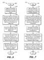
- FIG. 6illustrates a flow chart of a method of detecting variations in a spatially correlated parameter in accordance with an embodiment of the present invention
- FIG. 7illustrates a flow chart of a process for reducing the variance of a selected parameter of an integrated circuit die replicated on a silicon wafer in accordance with an embodiment of the present invention.
- a reticleis a finely resolved picture that often contains multiple images of the same die pattern.
- the die patterns in the reticleare transferred simultaneously from the reticle to the silicon wafer according to well known techniques of photolithography as the reticle image is stepped across the silicon wafer. Due to the effects on the light traveling through the reticle to the silicon wafer, the exact pattern is not perfectly maintained across all copies of the die pattern. The result of these effects are often related to the relative positions of the die patterns within the reticle. If these effects dominate a process step that would otherwise cause a continuous change in a parameter value, then the reticle dependence pattern results in a higher correlation of parameter values in non-adjacent die than in adjacent, or “nearest neighbor”, die.
- die-to-die correlations of a selected parametermay be calculated by averaging measured values of a selected parameter of die having an identical relative location with respect to a target location of each die on the silicon wafer respectively.
- a target locationis the location of a specific die on the silicon wafer.
- a relative locationis the location of a die displaced from the target location by a specific difference in the X-Y coordinates.
- An example of a relative locationis ( ⁇ 5,10), that is, 5 units in the negative-X direction and 10 units in the positive-Y direction with respect to the target location.
- the corresponding die having the relative location ( ⁇ 5,10)would have the X-Y coordinates ( 145 , 310 ).
- the corresponding die having the identical relative locationwould have the X-Y coordinates ( 615 , 232 ).
- the corresponding die having the identical relative locationwould have the X-Y coordinates ( 495 , 810 ), and so on.
- a single production lotprovides test data that allows for calculating die-to-die correlations of a selected parameter for each relative location from 5,000 to 10,000 or more times, an adequate sample is provided to obtain a highly resolved plot of the residual of the selected parameter as a function of relative location. Die having values of the selected parameter that exceed an expected value range may be identified as statistical outliers and rejected from the production lot, thereby increasing the average service life of the production lot.
- a highly resolved imagemay be obtained of not only the major spatially correlated patterns across the wafer, but also of more subtle patterns resulting from the manufacturing process.
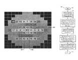
- FIG. 1illustrates a typical distribution of average die quiescent current for a replicated pattern of integrated circuit die on a silicon wafer. Shown in FIG. 1 are target die locations 102 and corresponding die relative locations 104 . A gray scale is used to indicate the variation of the quiescent current at each of the target die locations 102 .
- the variable gis an index that identifies the specific relative location 104 of a corresponding die with respect to each of the target die locations 102 .
- the variable granges from 1 to n, where n is selected to include as large or as small an area around each of the target die locations 102 as desired for correlating values of the selected parameter. In the illustrated example, n equals 49, and the selected parameter is quiescent current (Iddq), however, other values of n and other selected parameters may be used to suit specific applications.
- the residual of the selected parameteris calculated by measuring the value of the selected parameter at each of the target die locations 102 on the wafer and calculating the difference between the value of the selected parameter of a target die location 102 and the value of the selected parameter of the corresponding die at an identical relative location g with respect to each of the target die locations 102 to generate a distribution of differences.
- the measured values of the selected parameter at five of the target locations 102are 1.5, 1.2, 1.3, 1.6, and 0.9
- the measured values of the selected parameter at an identical relative location ( ⁇ 5, 10) with respect to each of the five target locations 102are 1.3, 1.1, 1.4, 1.5, and 1.3
- the average of the absolute value of the distribution of differences for an identical relative location gis defined as the residual of the relative location g.
- the absolute value of the distribution of differences in this exampleis 0.2, 0.1, 0.1, 0.1, and 0.4.
- the residual of the selected parameter for the relative location ( ⁇ 5, 10)is thus 0.18.
- the residual of each of relative locations 104may be calculated.
- FIG. 2Aillustrates a plot of residual quiescent current as a function of relative location according to an embodiment of the present invention representative of a smooth process variation. Shown in FIG. 2A are a target die location 102 and corresponding die locations 104 .
- a gray scaleis used to indicate the relative value of the residual quiescent current calculated for each of the identical relative locations 104 , where white indicates the lowest variation in the quiescent current with respect to the target die location 102 .
- the variation in residual quiescent currentincreases with distance from the target die X-Y location 102 , which identifies smooth process variation as the only spatial pattern.
- a nearest neighbor residual processmay be used according to well known techniques to identify statistical outliers.
- FIG. 2Billustrates a three-dimensional mesh of the plot in FIG. 2 A. Shown in FIG. 2B are a target die X-Y location 102 and neighboring die locations 104 .
- the gray scaleis further enhanced by adding a third dimension that emphasizes the spatial pattern of the residual quiescent current.
- FIG. 3Aillustrates a plot of residual quiescent current as a function of relative die location according to an embodiment of the present invention representative of a non-continuous process variation. Shown in FIG. 3A are a target die location 102 and corresponding die locations 104 .
- a gray scaleis used to indicate the relative value of the residual quiescent current calculated for each of the identical relative locations 104 , where white indicates the lowest variation in the quiescent current with respect to the target die location 102 .
- the variation in residual quiescent currentdoes not change monotonically with distance from the target die location 102 as in the example of FIG. 2 A.
- the spatial pattern of the residual quiescent current in this exampleis non-continuous, therefore the nearest neighbor residual process, although possible, may be significantly improved for identifying statistical outliers.
- a more accurate method of identifying statistical outliersis to use the mean value of the selected parameter as a function of relative location to determine a best estimate of the expected parameter for each relative location.
- FIG. 3Billustrates a three-dimensional mesh of the plot of FIG. 3 A.
- the description of FIG. 2Balso applies to FIG. 3 B.
- Plots similar to those of FIGS. 2A, 2 B, 3 A, and 3 Bmay be generated to identify spatially correlated parameters in other electronic circuits replicated on a common substrate and in a variety of applications in which a common element is replicated in a spatial pattern.
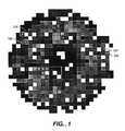
- FIG. 4illustrates an ordered rank of the top 40 die that are the most highly correlated with the target die from the location average results of FIGS. 3A and 3B. Shown in FIG. 4 are a target die 402 and corresponding die relative locations 404 numbered by correlation rank width the target die 402 .
- the relative locations most highly correlated with the target dielie on the same horizontal line as the target die.
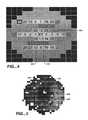
- FIG. 5illustrates average die quiescent current plotted as a function of wafer location with stepper/reticle effects. Shown in FIG. 5 are a target die 502 and corresponding die relative locations 504 .
- the gray scaleindicates the degree of correlation of average die quiescent current of the corresponding die relative locations 504 with the target die 502 . As shown in FIG. 5, there is a combination of smooth variation and row dependent variation in quiescent current.
- FIG. 6illustrates a flow chart 600 of a method of detecting variations in a spatially correlated parameter in accordance with an embodiment of the present invention.
- Step 602is the entry point for the flow chart 600 .
- a selected parameter of each of a plurality of electronic circuits replicated on a common substrateis measured according to well known techniques.
- the electronic circuitmay be, for example, an integrated circuit die.
- the inventionmay also be practiced with any implementation of an electronic circuit or other device such as a micro-machine that may be replicated on a common substrate, and the term “electronic circuit” as used herein includes all such types of devices including micro-machines that may be replicated on a common substrate.
- step 606a difference is calculated between a value of the selected parameter at a target location and that of an identical relative location with respect to the target location for each of the plurality of electronic circuits to generate a distribution of differences.
- step 608an absolute value of the distribution of differences is calculated.
- step 610an average of the absolute value of the distribution of differences is calculated to generate a representative value for the residual for the identical relative location.
- the calculated valueis the mean absolute error, or if the median is used, the median absolute error.
- Step 612is the exit point for the flow chart 600 .
- the method illustrated in FIG. 6may be used to detect spatial correlation of a variety of parameters of practically any device that may be replicated on a common substrate.
- FIG. 7illustrates a flow chart 700 of a process for reducing the variance of a selected parameter of an integrated circuit die replicated on a silicon wafer in accordance with an embodiment of the present invention.
- Step 702is the entry point for the flow chart 700 .
- a selected parameter of each of a plurality of integrated circuit die replicated on a wafer substrateis measured according to well known techniques.
- the selected parametermay be quiescent current (Iddq).
- a differenceis calculated between a value of the selected parameter at a target location and a that of an identical relative location with respect to the target location for each of the plurality of integrated circuit die to generate a distribution of differences.
- step 708an absolute value of the distribution of differences is calculated.
- an average of the absolute value of the distribution of differencesis calculated to generate a representative value for the identical relative location having an expected value range of the selected parameter at the identical relative location.
- the expected value rangemay be, for example, the value of the selected parameter at the target location plus or minus one-half the residual.
- step 712integrated circuit die at identical relative locations having a value of the selected parameter that lies outside the expected value range are rejected from the production lot.
- the die at the relative location ( ⁇ 5, 10) with respect to the first and the last of the five target locationswould be rejected as statistical outliers, since they have values of the selected parameter that lie outside the range 1.3 ⁇ 0.18.
- Other values for the expected value rangemay be used to suit specific applications.
- Step 714is the exit point for the flow chart 700 .
- the method illustrated in FIG. 7may be used to reduce the variation in a selected parameter in a production lot of integrated circuit dies, thereby increasing the reliability of the production lot.
- the lot averagingmay be performed for each wafer X-Y coordinate so that a new set of best estimates is re-calculated for each X-Y position. Re-calculating the best estimate locations includes the effects of edge die versus center die on the wafer.
- other wafers in the lotmay be utilized for the location averaging.
- the best estimates for a given X-Y locationmay be the identical location on another wafer in the lot. This technique may be improved by re-ordering the wafers in the sequence in which they were processed to ensure more accurate estimation.
Landscapes
- Engineering & Computer Science (AREA)
- Manufacturing & Machinery (AREA)
- Computer Hardware Design (AREA)
- Microelectronics & Electronic Packaging (AREA)
- Power Engineering (AREA)
- Testing Or Measuring Of Semiconductors Or The Like (AREA)
Abstract
Description
Claims (3)
Priority Applications (2)
| Application Number | Priority Date | Filing Date | Title |
|---|---|---|---|
| US10/020,407US6787379B1 (en) | 2001-12-12 | 2001-12-12 | Method of detecting spatially correlated variations in a parameter of an integrated circuit die |
| US10/640,778US6943042B2 (en) | 2001-12-12 | 2003-08-13 | Method of detecting spatially correlated variations in a parameter of an integrated circuit die |
Applications Claiming Priority (1)
| Application Number | Priority Date | Filing Date | Title |
|---|---|---|---|
| US10/020,407US6787379B1 (en) | 2001-12-12 | 2001-12-12 | Method of detecting spatially correlated variations in a parameter of an integrated circuit die |
Related Child Applications (1)
| Application Number | Title | Priority Date | Filing Date |
|---|---|---|---|
| US10/640,778ContinuationUS6943042B2 (en) | 2001-12-12 | 2003-08-13 | Method of detecting spatially correlated variations in a parameter of an integrated circuit die |
Publications (1)
| Publication Number | Publication Date |
|---|---|
| US6787379B1true US6787379B1 (en) | 2004-09-07 |
Family
ID=31713812
Family Applications (2)
| Application Number | Title | Priority Date | Filing Date |
|---|---|---|---|
| US10/020,407Expired - LifetimeUS6787379B1 (en) | 2001-12-12 | 2001-12-12 | Method of detecting spatially correlated variations in a parameter of an integrated circuit die |
| US10/640,778Expired - Fee RelatedUS6943042B2 (en) | 2001-12-12 | 2003-08-13 | Method of detecting spatially correlated variations in a parameter of an integrated circuit die |
Family Applications After (1)
| Application Number | Title | Priority Date | Filing Date |
|---|---|---|---|
| US10/640,778Expired - Fee RelatedUS6943042B2 (en) | 2001-12-12 | 2003-08-13 | Method of detecting spatially correlated variations in a parameter of an integrated circuit die |
Country Status (1)
| Country | Link |
|---|---|
| US (2) | US6787379B1 (en) |
Cited By (9)
| Publication number | Priority date | Publication date | Assignee | Title |
|---|---|---|---|---|
| US20040138846A1 (en)* | 2001-05-24 | 2004-07-15 | Buxton Paul M. | Methods and apparatus for data analysis |
| US20040267477A1 (en)* | 2001-05-24 | 2004-12-30 | Scott Michael J. | Methods and apparatus for data analysis |
| US20050278597A1 (en)* | 2001-05-24 | 2005-12-15 | Emilio Miguelanez | Methods and apparatus for data analysis |
| US20060085155A1 (en)* | 2001-05-24 | 2006-04-20 | Emilio Miguelanez | Methods and apparatus for local outlier detection |
| US20070219741A1 (en)* | 2005-05-20 | 2007-09-20 | Emilio Miguelanez | Methods and apparatus for hybrid outlier detection |
| US20080091977A1 (en)* | 2004-04-02 | 2008-04-17 | Emilio Miguelanez | Methods and apparatus for data analysis |
| US20080164898A1 (en)* | 2007-01-04 | 2008-07-10 | Samsung Electronics Co., Ltd. | Probe card for test of semiconductor chips and method for test of semiconductor chips using the same |
| US7437271B2 (en) | 2003-02-14 | 2008-10-14 | Test Advantage, Inc. | Methods and apparatus for data analysis |
| US20130057311A1 (en)* | 2011-09-01 | 2013-03-07 | Renesas Electronics Corporation | Screening method, screening device and program |
Families Citing this family (6)
| Publication number | Priority date | Publication date | Assignee | Title |
|---|---|---|---|---|
| IL161217A (en)* | 2004-04-01 | 2013-03-24 | Cvidya 2010 Ltd | Detection of outliers in communication networks |
| US8190391B2 (en)* | 2007-03-29 | 2012-05-29 | Globalfoundries Inc. | Determining die performance by incorporating neighboring die performance metrics |
| US20080262769A1 (en)* | 2007-04-23 | 2008-10-23 | Daniel Kadosh | Using multivariate health metrics to determine market segment and testing requirements |
| US8041518B2 (en)* | 2007-05-08 | 2011-10-18 | Globalfoundries Inc. | Determining die test protocols based on process health |
| US9207530B2 (en)* | 2010-02-23 | 2015-12-08 | Carl Zeiss Sms Ltd. | Analyses of measurement data |
| JP6049052B2 (en)* | 2012-07-20 | 2016-12-21 | 株式会社日立ハイテクノロジーズ | Wafer visual inspection apparatus and sensitivity threshold setting method in wafer visual inspection apparatus |
Citations (4)
| Publication number | Priority date | Publication date | Assignee | Title |
|---|---|---|---|---|
| US5889409A (en)* | 1996-09-27 | 1999-03-30 | Intel Corporation | Leakage tracking device sample for IDDQ measurement and defect resolution |
| US5889408A (en)* | 1996-06-27 | 1999-03-30 | Intel Corporation | Delta IDDQ testing |
| US6342790B1 (en)* | 2000-04-13 | 2002-01-29 | Pmc-Sierra, Inc. | High-speed, adaptive IDDQ measurement |
| US20020102747A1 (en)* | 2000-09-18 | 2002-08-01 | David Muradian | Correction of overlay offset between inspection layers in integrated circuits |
Family Cites Families (1)
| Publication number | Priority date | Publication date | Assignee | Title |
|---|---|---|---|---|
| US6023186A (en)* | 1996-04-30 | 2000-02-08 | Kabushiki Kaisha Toshiba | CMOS integrated circuit device and inspection method thereof |
- 2001
- 2001-12-12USUS10/020,407patent/US6787379B1/ennot_activeExpired - Lifetime
- 2003
- 2003-08-13USUS10/640,778patent/US6943042B2/ennot_activeExpired - Fee Related
Patent Citations (5)
| Publication number | Priority date | Publication date | Assignee | Title |
|---|---|---|---|---|
| US5889408A (en)* | 1996-06-27 | 1999-03-30 | Intel Corporation | Delta IDDQ testing |
| US6239606B1 (en)* | 1996-06-27 | 2001-05-29 | Intel Corporation | Method to perform IDDQ testing in the presence of high background leakage current |
| US5889409A (en)* | 1996-09-27 | 1999-03-30 | Intel Corporation | Leakage tracking device sample for IDDQ measurement and defect resolution |
| US6342790B1 (en)* | 2000-04-13 | 2002-01-29 | Pmc-Sierra, Inc. | High-speed, adaptive IDDQ measurement |
| US20020102747A1 (en)* | 2000-09-18 | 2002-08-01 | David Muradian | Correction of overlay offset between inspection layers in integrated circuits |
Non-Patent Citations (4)
| Title |
|---|
| Kruseman et al., "The future of delta IDDQ testing", International Test Conference, 2001, pp. 101-110.** |
| Sabade et al. "Improved wafer-level spatial analysis for IDDQ limit setting", Test Conference, 2001, Proceedings. International, pp. 82-91.** |
| Thibeault, C., "Improving delta-IDDQ-based test methods", International Test Conference, 2000, pp. 207-216.* |
| Thibeault, C., "On the Comparison of IDDQ and IDDQ Testing", VLSI Test Symposium, 1999, Proceedings. 17th IEEE, pp. 143-150.** |
Cited By (17)
| Publication number | Priority date | Publication date | Assignee | Title |
|---|---|---|---|---|
| US8878561B2 (en)* | 2001-02-01 | 2014-11-04 | Renesas Electronics Corporation | Screening method, screening device and program |
| US7395170B2 (en) | 2001-05-24 | 2008-07-01 | Test Advantage, Inc. | Methods and apparatus for data analysis |
| US8000928B2 (en) | 2001-05-24 | 2011-08-16 | Test Advantage, Inc. | Methods and apparatus for data analysis |
| US20060085155A1 (en)* | 2001-05-24 | 2006-04-20 | Emilio Miguelanez | Methods and apparatus for local outlier detection |
| US7225107B2 (en) | 2001-05-24 | 2007-05-29 | Test Advantage, Inc. | Methods and apparatus for data analysis |
| US20040267477A1 (en)* | 2001-05-24 | 2004-12-30 | Scott Michael J. | Methods and apparatus for data analysis |
| US7356430B2 (en) | 2001-05-24 | 2008-04-08 | Test Advantage, Inc. | Methods and apparatus for data analysis |
| US20050278597A1 (en)* | 2001-05-24 | 2005-12-15 | Emilio Miguelanez | Methods and apparatus for data analysis |
| US20080249742A1 (en)* | 2001-05-24 | 2008-10-09 | Scott Michael J | Methods and apparatus for data analysis |
| US8417477B2 (en) | 2001-05-24 | 2013-04-09 | Test Acuity Solutions, Inc. | Methods and apparatus for local outlier detection |
| US20040138846A1 (en)* | 2001-05-24 | 2004-07-15 | Buxton Paul M. | Methods and apparatus for data analysis |
| US7437271B2 (en) | 2003-02-14 | 2008-10-14 | Test Advantage, Inc. | Methods and apparatus for data analysis |
| US7904279B2 (en) | 2004-04-02 | 2011-03-08 | Test Advantage, Inc. | Methods and apparatus for data analysis |
| US20080091977A1 (en)* | 2004-04-02 | 2008-04-17 | Emilio Miguelanez | Methods and apparatus for data analysis |
| US20070219741A1 (en)* | 2005-05-20 | 2007-09-20 | Emilio Miguelanez | Methods and apparatus for hybrid outlier detection |
| US20080164898A1 (en)* | 2007-01-04 | 2008-07-10 | Samsung Electronics Co., Ltd. | Probe card for test of semiconductor chips and method for test of semiconductor chips using the same |
| US20130057311A1 (en)* | 2011-09-01 | 2013-03-07 | Renesas Electronics Corporation | Screening method, screening device and program |
Also Published As
| Publication number | Publication date |
|---|---|
| US20040033635A1 (en) | 2004-02-19 |
| US6943042B2 (en) | 2005-09-13 |
Similar Documents
| Publication | Publication Date | Title |
|---|---|---|
| US6787379B1 (en) | Method of detecting spatially correlated variations in a parameter of an integrated circuit die | |
| TWI731581B (en) | Methods of determining corrections for a patterning process, device manufacturing method, control system for a lithographic apparatus and lithographic apparatus | |
| US7933015B2 (en) | Mark for alignment and overlay, mask having the same, and method of using the same | |
| US5444538A (en) | System and method for optimizing the grid and intrafield registration of wafer patterns | |
| US6484060B1 (en) | Layout for measurement of overlay error | |
| US20050033467A1 (en) | Dynamic metrology sampling methods, and system for performing same | |
| US9176396B2 (en) | Overlay sampling methodology | |
| CN104736962A (en) | Method for estimating and correcting misregistration target inaccuracy | |
| KR20120092578A (en) | Unique mark and method to determine critical dimension uniformity and registration of reticles combined with wafer overlay capability | |
| US7627179B2 (en) | Image processing apparatus, image processing method, exposure apparatus, and device manufacturing method | |
| US6948149B2 (en) | Method of determining the overlay accuracy of multiple patterns formed on a semiconductor wafer | |
| EP1441258B1 (en) | Alignment method and overlay inspection method | |
| TW202043750A (en) | Parameter-stable misregistration measurement amelioration in semiconductor devices | |
| CN106154741B (en) | Mask plate, defocus testing method and defocus testing system | |
| US11640117B2 (en) | Selection of regions of interest for measurement of misregistration and amelioration thereof | |
| CN107561875B (en) | Overlay error measurement and problem assessment method | |
| JP2011192769A (en) | Method and system of manufacturing semiconductor device | |
| US20120274916A1 (en) | Exposure apparatus and device manufacturing method | |
| US11876022B2 (en) | Substrate treatment method and substrate treatment system | |
| JP7445003B2 (en) | Multi-step process inspection method | |
| JP7516203B2 (en) | SUBSTRATE PROCESSING METHOD AND SUBSTRATE PROCESSING SYSTEM | |
| TWI846977B (en) | Processing condition estimation device, processing condition estimation method, and processing condition estimation recording medium | |
| JPH0982612A (en) | Inspection method for overlay misalignment | |
| JP7587359B2 (en) | Alignment apparatus, method for determining position of mark, program, lithography apparatus, and article manufacturing method | |
| Lecarpentier et al. | Overlay measurement accuracy verification using CD-SEM and application to the quantification of WIS caused by BARC |
Legal Events
| Date | Code | Title | Description |
|---|---|---|---|
| AS | Assignment | Owner name:LSI LOGIC CORPORATION, CALIFORNIA Free format text:ASSIGNMENT OF ASSIGNORS INTEREST;ASSIGNORS:MADGE, ROBERT;COTA, KEVIN;WHITEFIELD, BRUCE;REEL/FRAME:012400/0019 Effective date:20011204 | |
| STCF | Information on status: patent grant | Free format text:PATENTED CASE | |
| FEPP | Fee payment procedure | Free format text:PAYOR NUMBER ASSIGNED (ORIGINAL EVENT CODE: ASPN); ENTITY STATUS OF PATENT OWNER: LARGE ENTITY | |
| FPAY | Fee payment | Year of fee payment:4 | |
| FPAY | Fee payment | Year of fee payment:8 | |
| AS | Assignment | Owner name:DEUTSCHE BANK AG NEW YORK BRANCH, AS COLLATERAL AG Free format text:PATENT SECURITY AGREEMENT;ASSIGNORS:LSI CORPORATION;AGERE SYSTEMS LLC;REEL/FRAME:032856/0031 Effective date:20140506 | |
| AS | Assignment | Owner name:LSI CORPORATION, CALIFORNIA Free format text:CHANGE OF NAME;ASSIGNOR:LSI LOGIC CORPORATION;REEL/FRAME:033102/0270 Effective date:20070406 | |
| AS | Assignment | Owner name:AVAGO TECHNOLOGIES GENERAL IP (SINGAPORE) PTE. LTD Free format text:ASSIGNMENT OF ASSIGNORS INTEREST;ASSIGNOR:LSI CORPORATION;REEL/FRAME:035390/0388 Effective date:20140814 | |
| AS | Assignment | Owner name:AGERE SYSTEMS LLC, PENNSYLVANIA Free format text:TERMINATION AND RELEASE OF SECURITY INTEREST IN PATENT RIGHTS (RELEASES RF 032856-0031);ASSIGNOR:DEUTSCHE BANK AG NEW YORK BRANCH, AS COLLATERAL AGENT;REEL/FRAME:037684/0039 Effective date:20160201 Owner name:LSI CORPORATION, CALIFORNIA Free format text:TERMINATION AND RELEASE OF SECURITY INTEREST IN PATENT RIGHTS (RELEASES RF 032856-0031);ASSIGNOR:DEUTSCHE BANK AG NEW YORK BRANCH, AS COLLATERAL AGENT;REEL/FRAME:037684/0039 Effective date:20160201 | |
| AS | Assignment | Owner name:BANK OF AMERICA, N.A., AS COLLATERAL AGENT, NORTH CAROLINA Free format text:PATENT SECURITY AGREEMENT;ASSIGNOR:AVAGO TECHNOLOGIES GENERAL IP (SINGAPORE) PTE. LTD.;REEL/FRAME:037808/0001 Effective date:20160201 Owner name:BANK OF AMERICA, N.A., AS COLLATERAL AGENT, NORTH Free format text:PATENT SECURITY AGREEMENT;ASSIGNOR:AVAGO TECHNOLOGIES GENERAL IP (SINGAPORE) PTE. LTD.;REEL/FRAME:037808/0001 Effective date:20160201 | |
| FPAY | Fee payment | Year of fee payment:12 | |
| AS | Assignment | Owner name:AVAGO TECHNOLOGIES GENERAL IP (SINGAPORE) PTE. LTD., SINGAPORE Free format text:TERMINATION AND RELEASE OF SECURITY INTEREST IN PATENTS;ASSIGNOR:BANK OF AMERICA, N.A., AS COLLATERAL AGENT;REEL/FRAME:041710/0001 Effective date:20170119 Owner name:AVAGO TECHNOLOGIES GENERAL IP (SINGAPORE) PTE. LTD Free format text:TERMINATION AND RELEASE OF SECURITY INTEREST IN PATENTS;ASSIGNOR:BANK OF AMERICA, N.A., AS COLLATERAL AGENT;REEL/FRAME:041710/0001 Effective date:20170119 | |
| AS | Assignment | Owner name:BELL SEMICONDUCTOR, LLC, ILLINOIS Free format text:ASSIGNMENT OF ASSIGNORS INTEREST;ASSIGNORS:AVAGO TECHNOLOGIES GENERAL IP (SINGAPORE) PTE. LTD.;BROADCOM CORPORATION;REEL/FRAME:044886/0608 Effective date:20171208 | |
| AS | Assignment | Owner name:CORTLAND CAPITAL MARKET SERVICES LLC, AS COLLATERA Free format text:SECURITY INTEREST;ASSIGNORS:HILCO PATENT ACQUISITION 56, LLC;BELL SEMICONDUCTOR, LLC;BELL NORTHERN RESEARCH, LLC;REEL/FRAME:045216/0020 Effective date:20180124 | |
| AS | Assignment | Owner name:BELL NORTHERN RESEARCH, LLC, ILLINOIS Free format text:RELEASE BY SECURED PARTY;ASSIGNOR:CORTLAND CAPITAL MARKET SERVICES LLC;REEL/FRAME:059720/0719 Effective date:20220401 Owner name:BELL SEMICONDUCTOR, LLC, ILLINOIS Free format text:RELEASE BY SECURED PARTY;ASSIGNOR:CORTLAND CAPITAL MARKET SERVICES LLC;REEL/FRAME:059720/0719 Effective date:20220401 Owner name:HILCO PATENT ACQUISITION 56, LLC, ILLINOIS Free format text:RELEASE BY SECURED PARTY;ASSIGNOR:CORTLAND CAPITAL MARKET SERVICES LLC;REEL/FRAME:059720/0719 Effective date:20220401 |