US6785000B2 - Bulk optical interferometer - Google Patents
Bulk optical interferometerDownload PDFInfo
- Publication number
- US6785000B2 US6785000B2US10/177,668US17766802AUS6785000B2US 6785000 B2US6785000 B2US 6785000B2US 17766802 AUS17766802 AUS 17766802AUS 6785000 B2US6785000 B2US 6785000B2
- Authority
- US
- United States
- Prior art keywords
- sub
- channels
- resonator
- ring resonator
- output
- Prior art date
- Legal status (The legal status is an assumption and is not a legal conclusion. Google has not performed a legal analysis and makes no representation as to the accuracy of the status listed.)
- Expired - Fee Related, expires
Links
- 230000003287optical effectEffects0.000titleclaimsabstractdescription41
- 238000000576coating methodMethods0.000claimsdescription26
- 239000011248coating agentSubstances0.000claimsdescription20
- 239000000758substrateSubstances0.000claimsdescription15
- 238000004519manufacturing processMethods0.000claimsdescription3
- 230000002452interceptive effectEffects0.000claimsdescription2
- 230000001934delayEffects0.000claims1
- 241001270131Agaricus moelleriSpecies0.000abstractdescription2
- 230000005540biological transmissionEffects0.000abstractdescription2
- 239000011521glassSubstances0.000description2
- 238000002310reflectometryMethods0.000description2
- 230000003595spectral effectEffects0.000description2
- 238000000411transmission spectrumMethods0.000description2
- 230000000295complement effectEffects0.000description1
- 239000013078crystalSubstances0.000description1
- 230000007423decreaseEffects0.000description1
- 230000001066destructive effectEffects0.000description1
- 239000000463materialSubstances0.000description1
- 238000000034methodMethods0.000description1
- 238000012986modificationMethods0.000description1
- 230000004048modificationEffects0.000description1
- 239000013307optical fiberSubstances0.000description1
- 230000010287polarizationEffects0.000description1
Images


Classifications
- G—PHYSICS
- G02—OPTICS
- G02B—OPTICAL ELEMENTS, SYSTEMS OR APPARATUS
- G02B6/00—Light guides; Structural details of arrangements comprising light guides and other optical elements, e.g. couplings
- G02B6/24—Coupling light guides
- G02B6/26—Optical coupling means
- G02B6/28—Optical coupling means having data bus means, i.e. plural waveguides interconnected and providing an inherently bidirectional system by mixing and splitting signals
- G02B6/293—Optical coupling means having data bus means, i.e. plural waveguides interconnected and providing an inherently bidirectional system by mixing and splitting signals with wavelength selective means
- G02B6/29346—Optical coupling means having data bus means, i.e. plural waveguides interconnected and providing an inherently bidirectional system by mixing and splitting signals with wavelength selective means operating by wave or beam interference
- G02B6/29347—Loop interferometers, e.g. Sagnac, loop mirror
Definitions
- the present applicationrelates to an optical interferometer, and in particular to a bulk optical interferometer based on a Mach-Zehnder interferometer (MZI) for use as a wavelength channel interleaver/de-interleaver.
- MZIMach-Zehnder interferometer
- Optical interleaversare becoming a popular tool in dense wavelength division multiplexed (DWDM) communications networks as an interface between components designed for signals with a first wavelength channel spacing and components designed for signals with a second wavelength channel spacing.
- DWDMdense wavelength division multiplexed
- 100 GHz channel spacingbecame the standard.
- 50 GHz channels spacing and even 25 GHz channel spacingwill become common place.
- conventional de-multiplexing filterse.g. dichroic filters
- optical interleaversare used to separate the closely spaced channels into two sets of channels, which are twice as far apart. This process can continue until the channels are far enough apart for conventional multiplexing to be effective.
- Interleavershave taken several different forms including: Birefringent Crystal Interleavers (BCI) such as the one disclosed in U.S. Pat. No. 6,301,046 issued Oct. 9, 2001 in the name of Kuochou Tai et al; Integrated Lattice Filter Interleavers such as the one disclosed in U.S. Pat. No. 5,596,661 issued Jan. 21, 1997 in the name of Charles Henry; and Michelson Gires-Tournois Interleavers (MGTI) such as the ones disclosed in U.S. Pat. No. 6,304,689 issued Oct. 16, 2001 in the name of Benjaminumblel et al., U.S. Pat. No. 6,252,716 issued Jun.
- BCIBirefringent Crystal Interleavers
- MGTIMichelson Gires-Tournois Interleavers
- An object of the present inventionis to overcome the shortcomings of the prior art and provide a simple bulk optical interleaver with very few parts that is easily manufactured at low cost and provides reliable and stable performance.
- an optical interferometer devicecomprising:
- a first beam-splitterfor separating the input optical beam into first and second sub-beams traveling along first and second paths, respectively;
- a first ring resonatorpositioned in the first path including at least two substantially fully reflective surfaces and a first partially reflective surface, the first partially reflective surface for passing a portion of the first sub-beam into the first ring resonator, while reflecting the remainder of the first sub-beam away therefrom, whereby light exiting the first ring resonator is combined with the remainder of the first sub-beam forming a first recombined sub-beam;
- a second ring resonatorpositioned in the second path including at least two substantially fully reflective surfaces and a second partially reflective surface, the second partially reflective surface for passing a portion of the second sub-beam into the second ring resonator, while reflecting the remainder of the second sub-beam away therefrom, whereby light exiting the second ring resonator is combined with the remainder of the second sub-beam forming a second recombined sub-beam;
- a second beam splitterfor receiving the first and second recombined sub-beams resulting in the interference thereof and the production of a first output beam and a second output beam;
- a second output portfor outputting the second output beam.
- Another aspect of the present inventionrelates to a Mach-Zehnder interferometer comprising:
- a beam splitterfor separating an input beam of light into a first sub-beam and a second sub-beam, and for directing the first and second sub-beams along first and second arms, respectively, of the interferometer;
- a first ring resonator in the first arm of the interferometerhaving a first resonator delay for effecting the phase response of the first sub-beam
- a second ring resonator in the second arm of the interferometerhaving a second resonator delay for effecting the phase response of the second sub-beam
- a beam combiner/splitterfor interfering the first and second sub-beams resulting in first and second output beams.
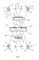
- FIG. 1is a schematic representation of one embodiment of an interferometer according to the present invention.
- FIG. 2is a schematic representation of another embodiment of an interferometer according to the present invention.
- FIGS. 3 a and 3 billustrate alternative examples of ring resonators useable in the embodiments of FIGS. 1 and 2;
- FIG. 4illustrates a transmission spectrum showing both sets of channels from an optical interleaver in accordance with one embodiment of the present invention
- FIG. 5illustrates a transmission spectrum showing both sets of channels from an optical interleaver in accordance with another embodiment of the present invention.
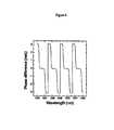
- FIG. 6is a plot of Phase Difference vs Wavelength for one set of the channels from an optical interleaver in accordance with the one embodiment of the present invention.
- the interferometeris based on a Mach Zehnder interferometer (MZI) into and out of which light can be launched via one or more of four ports 11 , 12 , 13 and 14 .
- MZIMach Zehnder interferometer
- Each portincludes a collimating/focusing lens 16 optically coupled to a ferrule 17 encasing an end of an optical fiber waveguide 18
- first port 11 and output via second and third ports 12 and 13respectively.
- various other combinationsare possible, including: input the second and/or third ports 12 and 13 , respectively and output the first and/or fourth ports 11 and 14 , respectively.
- the input light beam 20is launched via the first port 11 and gets split into a first sub-beam 21 and a second sub-beam 22 by a beam-splitter in the form of a first beam splitting coating 23 a on a portion of one side of a first glass (or other transparent) substrate 24 .
- the first beam splitting coating 23 asplits the input light beam 20 is half, i.e. the reflectance ranges between 42% and 50%, and ideally 50%.
- the first sub-beam 21passes through the first substrate 24 until intersecting a first partially-reflective surface 26 applied to an opposite side of the first substrate 24 .
- the reflectance of the first partially-reflective surface 26is preferably between 42% and 50%.
- a portion of the first sub-beam 21passes into a first ring resonator 27 , which includes a first mirror 31 and a second mirror 32 .
- Light exiting from the first ring resonator 27 after traveling a first resonator delay distanceis combined with light reflected by the first partially reflective coating 26 forming a recombined first sub-beam 33 .
- the recombined sub-beam 33is directed back through the first substrate 24 .
- the second sub-beam 22is reflected by the first beam splitting coating 23 a through a second glass (or other transparent) substrate 34 for intersection with a second partially-reflective surface 36 applied thereto.
- the reflectance of the second partially-reflective surface 36is preferably between 2.4% and 5.2%.
- a portion of the second sub-beam 22passes into a second ring resonator 37 , which includes a first mirror 41 and a second mirror 42 . Light leaving the second ring resonator 37 after traveling a second ring delay distance is combined with light reflected by the second partially reflective surface 36 , and directed towards the first substrate 24 forming a second recombined sub-beam 38 .
- the second recombined sub-beam 38interferes with the first recombined sub-beam 33 at a second beam splitting coating 23 b resulting in a portion of the light, i.e. a first output beam, being output the second port 12 and the remainder of the light, i.e. a second output beam, being output the third port 13 .
- the reflectance of the second beam splitting coating 23 balso ranges from 43% to 50%, and is ideally 50%.
- the first and second beam splitting coatings 23 a and 23 bcould have the same reflectance, e.g. 50%, and be applied simultaneously.
- the optical path from the first beam splitting coating 23 a to the first partially-reflective surface 26 back to the second beam splitting coating 22 bis defined as a first optical path of the Mach-Zehnder interferometer.
- the optical path from the first beam splitting coating 23 a to the second partially-reflective surface 26 back to the second beam splitting coating 22 bis defined as a second optical path of the Mach-Zehnder interferometer.
- the first optical pathhas a different length than the second optical path. This difference is call an optical path length difference.
- the optical path with the partially reflective surface having the lower reflectivitye.g.
- one set of wavelength channelse.g. the even ITU channels
- another set of wavelength channelse.g. the odd ITU channels
- FIG. 2illustrates an alternative embodiment of the present invention in which a minimum amount of substrate material is used.
- New first and second substrates 124 and 134are substantially thinner than there counterparts 24 and 34 from FIG. 1 .
- a third substrate 144is required for supporting the first partially reflective coating 26 .
- the substrate 124can also be divided into two separate substrates, each one having one of the beam splitting coatings 23 a and 23 b.
- FIGS. 3 a and 3 billustrate two other examples of ring resonators for use in place of the first and second ring resonators 27 and 37 .
- Ring resonator 137(FIG. 3 a ) includes the second substrate 34 and the second partially reflective coating 36 , along with three reflective surfaces 141 , 142 and 143 . As is obvious to one skilled in the art, any number of reflective surfaces could be used.
- FIG. 3 billustrates the second ring resonator 37 with the addition of a wedge-shaped tuning plate 150 .
- the tuning plate 150which has an index of refraction different than air, can be used to make small adjustments to the optical path length of one of the ring resonators to match the two ring resonators appropriately. Lateral adjustment of the wedge-shaped tuning plate 150 will result in the beam of light traveling through more or less thereof, which increases or decreases the optical path length of the ring resonator.
- FIGS. 4 and 5illustrate theoretical transmission spectral responses for interleavers according to the present invention.
- the solid linerepresents the even ITU wavelength channels, while the dotted line represents the odd ITU wavelength channels.
- the bandwidth of the pass-band at ⁇ 0.5 dBis over 85% of the free spectral range (FSR) of the interleaver, and the bandwidth of the stop-band at ⁇ 25 dB is over 75% of the FSR of the interleaver.
- FSRfree spectral range
- the reflectance of the first and second beam splitting coatings 23 a and 23 bare 50% and 48.3, respectively, and the reflectance of the first and second partially-reflective coatings 26 and 36 are 44.8% and 3.4%, respectively.
- the reflectance of the first and second beam splitting coatings 23 a and 23 bare both 50%, and the reflectance of the first and second paitially-reflective coatings 26 and 36 are 42.2% and 3.3%, respectively.
- the plot illustrated in FIG. 6shows the phase difference of the odd ITU wavelength channels for an interleaver according to the present invention.
- the phase differencealternates between 0 and ⁇ over consecutive wavelength channels equivalent to the FSR of the optical interleaver.
- the horizontal segments of the plot with 0 phase differencerepresent sections of constructive interference, i.e. flattop passbands, while the horizontal segments of the plot with ⁇ phase differences represent sections of destructive interference, i.e. stop-bands.
- the device according to the present inventioncan also be used to de-interleave two sets of complementary wavelength channels.
- Two input beamseach one comprising one of the complimentary sets of wavelength channels, are input the second and third ports 12 and 13 , respectively (or the first and fourth ports 11 and 14 ), and directed at the beam splitter where they are interfered and separated into two sub-beams.
- Each of the sub-beamstravels to a different one of the ring resonators 27 or 37 forming two recombined sub-beams, which are then combined at the beam splitter, and output the first or fourth port, 11 or 14 (or the second or third port, 12 or 13 ).
Landscapes
- Physics & Mathematics (AREA)
- General Physics & Mathematics (AREA)
- Optics & Photonics (AREA)
- Optical Modulation, Optical Deflection, Nonlinear Optics, Optical Demodulation, Optical Logic Elements (AREA)
- Optical Integrated Circuits (AREA)
Abstract
Description
Claims (15)
Priority Applications (1)
| Application Number | Priority Date | Filing Date | Title |
|---|---|---|---|
| US10/177,668US6785000B2 (en) | 2002-06-24 | 2002-06-24 | Bulk optical interferometer |
Applications Claiming Priority (1)
| Application Number | Priority Date | Filing Date | Title |
|---|---|---|---|
| US10/177,668US6785000B2 (en) | 2002-06-24 | 2002-06-24 | Bulk optical interferometer |
Publications (2)
| Publication Number | Publication Date |
|---|---|
| US20030234935A1 US20030234935A1 (en) | 2003-12-25 |
| US6785000B2true US6785000B2 (en) | 2004-08-31 |
Family
ID=29734459
Family Applications (1)
| Application Number | Title | Priority Date | Filing Date |
|---|---|---|---|
| US10/177,668Expired - Fee RelatedUS6785000B2 (en) | 2002-06-24 | 2002-06-24 | Bulk optical interferometer |
Country Status (1)
| Country | Link |
|---|---|
| US (1) | US6785000B2 (en) |
Cited By (6)
| Publication number | Priority date | Publication date | Assignee | Title |
|---|---|---|---|---|
| US20070057085A1 (en)* | 2005-09-14 | 2007-03-15 | Trompen Mick A | Dispenser |
| US9648254B2 (en)* | 2014-03-21 | 2017-05-09 | Hypermed Imaging, Inc. | Compact light sensor |
| US9655519B2 (en) | 2014-03-21 | 2017-05-23 | Hypermed Imaging, Inc. | Systems and methods for performing an imaging test under constrained conditions |
| US10574361B2 (en) | 2015-08-06 | 2020-02-25 | Hewlett Packard Enterprise Development Lp | Optical phase modulators |
| US10798310B2 (en) | 2016-05-17 | 2020-10-06 | Hypermed Imaging, Inc. | Hyperspectral imager coupled with indicator molecule tracking |
| US20230106876A1 (en)* | 2021-10-01 | 2023-04-06 | Lumentum Operations Llc | Bidirectional filter |
Families Citing this family (2)
| Publication number | Priority date | Publication date | Assignee | Title |
|---|---|---|---|---|
| US6891994B2 (en)* | 2002-10-21 | 2005-05-10 | Stratos International, Inc. | Micro optical design for DWDM interleavers with narrow channel spacing |
| US7009708B1 (en)* | 2003-02-25 | 2006-03-07 | Lockheed Martin Corporation | Symmetric periscope for concentric beam configuration in an ultra-high precision laser interferometric beam launcher |
Citations (7)
| Publication number | Priority date | Publication date | Assignee | Title |
|---|---|---|---|---|
| US5596661A (en) | 1994-12-28 | 1997-01-21 | Lucent Technologies Inc. | Monolithic optical waveguide filters based on Fourier expansion |
| US6169604B1 (en) | 1999-02-10 | 2001-01-02 | Avanex Corporation | Nonlinear interferometer for fiber optic dense wavelength division multiplexer utilizing a phase bias element to separate wavelengths in an optical signal |
| US6243200B1 (en) | 2000-03-02 | 2001-06-05 | Chorum Technologies, Inc. | Optical wavelength router based on polarization interferometer |
| US6252716B1 (en) | 1999-07-22 | 2001-06-26 | Jds Uniphase Photonics C.V. | Bulk optic interleaver |
| US6301046B1 (en) | 1999-12-31 | 2001-10-09 | Jds Uniphase Corporation | Interleaver/deinterleavers causing little or no dispersion of optical signals |
| US6304689B1 (en) | 1998-01-09 | 2001-10-16 | Communications Research Laboratory Ministry Of Posts And Telecommunications | General multi-function optical filter |
| US20020171908A1 (en)* | 2001-02-27 | 2002-11-21 | Jds Uniphase Corporation | Low dispersion interleaver |
- 2002
- 2002-06-24USUS10/177,668patent/US6785000B2/ennot_activeExpired - Fee Related
Patent Citations (7)
| Publication number | Priority date | Publication date | Assignee | Title |
|---|---|---|---|---|
| US5596661A (en) | 1994-12-28 | 1997-01-21 | Lucent Technologies Inc. | Monolithic optical waveguide filters based on Fourier expansion |
| US6304689B1 (en) | 1998-01-09 | 2001-10-16 | Communications Research Laboratory Ministry Of Posts And Telecommunications | General multi-function optical filter |
| US6169604B1 (en) | 1999-02-10 | 2001-01-02 | Avanex Corporation | Nonlinear interferometer for fiber optic dense wavelength division multiplexer utilizing a phase bias element to separate wavelengths in an optical signal |
| US6252716B1 (en) | 1999-07-22 | 2001-06-26 | Jds Uniphase Photonics C.V. | Bulk optic interleaver |
| US6301046B1 (en) | 1999-12-31 | 2001-10-09 | Jds Uniphase Corporation | Interleaver/deinterleavers causing little or no dispersion of optical signals |
| US6243200B1 (en) | 2000-03-02 | 2001-06-05 | Chorum Technologies, Inc. | Optical wavelength router based on polarization interferometer |
| US20020171908A1 (en)* | 2001-02-27 | 2002-11-21 | Jds Uniphase Corporation | Low dispersion interleaver |
Non-Patent Citations (1)
| Title |
|---|
| US patent application 10/058,534 to Copner et al.* |
Cited By (12)
| Publication number | Priority date | Publication date | Assignee | Title |
|---|---|---|---|---|
| US20070057085A1 (en)* | 2005-09-14 | 2007-03-15 | Trompen Mick A | Dispenser |
| US9648254B2 (en)* | 2014-03-21 | 2017-05-09 | Hypermed Imaging, Inc. | Compact light sensor |
| US9655519B2 (en) | 2014-03-21 | 2017-05-23 | Hypermed Imaging, Inc. | Systems and methods for performing an imaging test under constrained conditions |
| US9746377B2 (en) | 2014-03-21 | 2017-08-29 | Hypermed Imaging, Inc. | Compact light sensor |
| US10205892B2 (en) | 2014-03-21 | 2019-02-12 | Hypermed Imaging, Inc. | Compact light sensor |
| US10652481B2 (en) | 2014-03-21 | 2020-05-12 | Hypermed Imaging, Inc. | Compact light sensor |
| US11159750B2 (en) | 2014-03-21 | 2021-10-26 | Hypermed Imaging, Inc. | Compact light sensor |
| US11399716B2 (en) | 2014-03-21 | 2022-08-02 | Hypermed Imaging, Inc. | Systems and methods for performing an imaging test under constrained conditions |
| US10574361B2 (en) | 2015-08-06 | 2020-02-25 | Hewlett Packard Enterprise Development Lp | Optical phase modulators |
| US10798310B2 (en) | 2016-05-17 | 2020-10-06 | Hypermed Imaging, Inc. | Hyperspectral imager coupled with indicator molecule tracking |
| US20230106876A1 (en)* | 2021-10-01 | 2023-04-06 | Lumentum Operations Llc | Bidirectional filter |
| US12001057B2 (en)* | 2021-10-01 | 2024-06-04 | Lumentum Operations Llc | Bidirectional filter |
Also Published As
| Publication number | Publication date |
|---|---|
| US20030234935A1 (en) | 2003-12-25 |
Similar Documents
| Publication | Publication Date | Title |
|---|---|---|
| US6125220A (en) | Interferometric optical device including a resonant optical cavity | |
| US6339474B2 (en) | Interferometric optical device including an optical resonator | |
| US6690513B2 (en) | Rhomb interleaver | |
| US6690846B2 (en) | Dispersion-compensated optical wavelength router | |
| US6765679B2 (en) | Multi-cavity interferometer with dispersion compensating resonators | |
| CA2340777A1 (en) | Optical signal interleaver | |
| CA2372906A1 (en) | Low dispersion interleaver | |
| US6907167B2 (en) | Optical interleaving with enhanced spectral response and reduced polarization sensitivity | |
| WO2002091045A2 (en) | Compact tunable optical wavelength interleaver | |
| US6748142B2 (en) | Integrated optical dual dispersion compensator for compensating both chromatic and polarization mode dispersion | |
| US7173763B2 (en) | Optical interleaver and filter cell design with enhanced clear aperture | |
| US6621632B2 (en) | Optical interferometer for demultiplexing an optical signal | |
| US6785000B2 (en) | Bulk optical interferometer | |
| US6871022B2 (en) | Cascaded optical multiplexer | |
| US6684002B2 (en) | Method and apparatus for an optical filter | |
| US6850364B2 (en) | Method and apparatus for an optical multiplexer and demultiplexer with an optical processing loop | |
| US6624939B2 (en) | 50/100 and 50/200 GHz de-interleaver with high isolation and dispersion compensation | |
| US20020154313A1 (en) | Optical interferometer for multiplexing optical signals | |
| EP1126293A2 (en) | Multiplexing/demultiplexing optical circuit | |
| WO2001084200A2 (en) | Optical wdm device having polarization elements | |
| US20020094157A1 (en) | Polarization dependent filtering device utilizing a fabry-perot cavity | |
| US8929700B2 (en) | Single-package dual optical-function device | |
| CN1288464C (en) | Bulk optical interferometer | |
| US7924505B1 (en) | Free-space hitlessly switchable optical interleaver | |
| US20140226164A1 (en) | Low-dispersion step-phase interferometer |
Legal Events
| Date | Code | Title | Description |
|---|---|---|---|
| AS | Assignment | Owner name:CASIX INC., CHINA Free format text:ASSIGNMENT OF ASSIGNORS INTEREST;ASSIGNORS:LIANG, FENG;ZHENG, HEPING;WU, LI;AND OTHERS;REEL/FRAME:013806/0160;SIGNING DATES FROM 20020625 TO 20020628 | |
| AS | Assignment | Owner name:JDS UNIPHASE CORPORATION, CALIFORNIA Free format text:ASSIGNMENT OF ASSIGNORS INTEREST;ASSIGNOR:CASIX INC.;REEL/FRAME:013811/0478 Effective date:20020615 | |
| FPAY | Fee payment | Year of fee payment:4 | |
| REMI | Maintenance fee reminder mailed | ||
| FPAY | Fee payment | Year of fee payment:8 | |
| AS | Assignment | Owner name:LUMENTUM OPERATIONS LLC, CALIFORNIA Free format text:ASSIGNMENT OF ASSIGNORS INTEREST;ASSIGNOR:JDS UNIPHASE CORPORATION;REEL/FRAME:036420/0340 Effective date:20150731 | |
| FEPP | Fee payment procedure | Free format text:PAYOR NUMBER ASSIGNED (ORIGINAL EVENT CODE: ASPN); ENTITY STATUS OF PATENT OWNER: LARGE ENTITY | |
| AS | Assignment | Owner name:LUMENTUM OPERATIONS LLC, CALIFORNIA Free format text:CORRECTIVE ASSIGNMENT TO CORRECT INCORRECT PATENTS 7,868,247 AND 6,476,312 ON PAGE A-A33 PREVIOUSLY RECORDED ON REEL 036420 FRAME 0340. ASSIGNOR(S) HEREBY CONFIRMS THE ASSIGNMENT;ASSIGNOR:JDS UNIPHASE CORPORATION;REEL/FRAME:037562/0513 Effective date:20150731 Owner name:LUMENTUM OPERATIONS LLC, CALIFORNIA Free format text:CORRECTIVE ASSIGNMENT TO CORRECT THE PATENTS LISTED ON PAGE A-A33 PREVIOUSLY RECORDED ON REEL 036420 FRAME 0340. ASSIGNOR(S) HEREBY CONFIRMS THE PATENT NUMBERS 7,868,247 AND 6,476,312 WERE LISTED IN ERROR AND SHOULD BE REMOVED;ASSIGNOR:JDS UNIPHASE CORPORATION;REEL/FRAME:037562/0513 Effective date:20150731 | |
| AS | Assignment | Owner name:LUMENTUM OPERATIONS LLC, CALIFORNIA Free format text:CORRECTIVE ASSIGNMENT TO CORRECT THE PATENTS LISTED ON PAGE A-A33 PATENT NUMBERS 7,868,247 AND 6,476,312 WERE LISTED IN ERROR AND SHOULD BE REMOVED. PREVIOUSLY RECORDED ON REEL 036420 FRAME 0340. ASSIGNOR(S) HEREBY CONFIRMS THE ASSIGNMENT;ASSIGNOR:JDS UNIPHASE CORPORATION;REEL/FRAME:037627/0641 Effective date:20150731 Owner name:LUMENTUM OPERATIONS LLC, CALIFORNIA Free format text:CORRECTIVE ASSIGNMENT TO CORRECT PATENTS 7,868,247 AND 6,476,312 LISTED ON PAGE A-A33 PREVIOUSLY RECORDED ON REEL 036420 FRAME 0340. ASSIGNOR(S) HEREBY CONFIRMS THE ASSIGNMENT;ASSIGNOR:JDS UNIPHASE CORPORATION;REEL/FRAME:037627/0641 Effective date:20150731 | |
| REMI | Maintenance fee reminder mailed | ||
| LAPS | Lapse for failure to pay maintenance fees | ||
| STCH | Information on status: patent discontinuation | Free format text:PATENT EXPIRED DUE TO NONPAYMENT OF MAINTENANCE FEES UNDER 37 CFR 1.362 | |
| FP | Lapsed due to failure to pay maintenance fee | Effective date:20160831 | |
| FEPP | Fee payment procedure | Free format text:PAYER NUMBER DE-ASSIGNED (ORIGINAL EVENT CODE: RMPN); ENTITY STATUS OF PATENT OWNER: LARGE ENTITY Free format text:PAYOR NUMBER ASSIGNED (ORIGINAL EVENT CODE: ASPN); ENTITY STATUS OF PATENT OWNER: LARGE ENTITY |