US6784982B1 - Direct mapping of DNA chips to detector arrays - Google Patents
Direct mapping of DNA chips to detector arraysDownload PDFInfo
- Publication number
- US6784982B1 US6784982B1US09/434,027US43402799AUS6784982B1US 6784982 B1US6784982 B1US 6784982B1US 43402799 AUS43402799 AUS 43402799AUS 6784982 B1US6784982 B1US 6784982B1
- Authority
- US
- United States
- Prior art keywords
- light
- chip
- sample surface
- detector
- sample
- Prior art date
- Legal status (The legal status is an assumption and is not a legal conclusion. Google has not performed a legal analysis and makes no representation as to the accuracy of the status listed.)
- Expired - Lifetime
Links
Images


Classifications
- G—PHYSICS
- G06—COMPUTING OR CALCULATING; COUNTING
- G06T—IMAGE DATA PROCESSING OR GENERATION, IN GENERAL
- G06T1/00—General purpose image data processing
- G06T1/0007—Image acquisition
- B—PERFORMING OPERATIONS; TRANSPORTING
- B01—PHYSICAL OR CHEMICAL PROCESSES OR APPARATUS IN GENERAL
- B01J—CHEMICAL OR PHYSICAL PROCESSES, e.g. CATALYSIS OR COLLOID CHEMISTRY; THEIR RELEVANT APPARATUS
- B01J2219/00—Chemical, physical or physico-chemical processes in general; Their relevant apparatus
- B01J2219/00274—Sequential or parallel reactions; Apparatus and devices for combinatorial chemistry or for making arrays; Chemical library technology
- B01J2219/00277—Apparatus
- B01J2219/00497—Features relating to the solid phase supports
- B01J2219/00527—Sheets
- B01J2219/00529—DNA chips
- B—PERFORMING OPERATIONS; TRANSPORTING
- B01—PHYSICAL OR CHEMICAL PROCESSES OR APPARATUS IN GENERAL
- B01J—CHEMICAL OR PHYSICAL PROCESSES, e.g. CATALYSIS OR COLLOID CHEMISTRY; THEIR RELEVANT APPARATUS
- B01J2219/00—Chemical, physical or physico-chemical processes in general; Their relevant apparatus
- B01J2219/00274—Sequential or parallel reactions; Apparatus and devices for combinatorial chemistry or for making arrays; Chemical library technology
- B01J2219/0068—Means for controlling the apparatus of the process
- B01J2219/00702—Processes involving means for analysing and characterising the products
Definitions
- a DNA chipis a rigid flat surface, typically glass or silicon, with short chains of related nucleic acids spotted in rows and columns on it. Hybridization between a fluorescently-labeled DNA and specific locations on the chip can be detected and analyzed by computer-based instrumentation. The information derived from the results of hybridization to DNA chips is stimulating advances in drug development, gene discovery, gene therapy, gene expression, genetic counseling, and plant biotechnology.
- Chip dimensionsthe number of sites of DNA deposition (sometimes termed “addresses”) per chip, and the width of the DNA spot per “address” are dependent upon the technologies employed for deposition.
- the most commonly used technologiesproduce spots with diameters of 50-300 ⁇ m.
- Photolithographyproduces spots that can have diameters as small as 1 micron. Technologies for making such chips are known to those skilled in these arts and arc described, for instance, in U.S. Pat. Nos. 5,925,525, 5,919,523, 5,837,832, and 5,744,305, which are incorporated herein by reference.
- Hybridization to DNA chipscan be monitored by fluorescence optics, by radioisotope detection, and by mass spectrometry.
- the most widely-used method for detection of hybridizationemploys fluorescently-labeled DNA, and a computerized system featuring a confocal fluorescence microscope (or an epifluorescence microscope), a movable microscope stage, and DNA detection software.
- a computerized systemfeaturing a confocal fluorescence microscope (or an epifluorescence microscope), a movable microscope stage, and DNA detection software.
- these conventional approaches to visualizing the surface of a DNA chipinvolve placing the chip on a microscope stage, moving the stage to put the sample into focus with a microscope objective, and triggering a digital camera or similar device to capture an image.
- An objectiveis a device made of a group of lenses that have a sophisticated design that collects light from the sample, magnifies the image of the sample, and minimizes the unavoidable image and color distortion caused by the passage of the light through the objective.
- the light-collected from the samplepasses through the objective and through a set of mirrors and lenses until is delivered to an eyepiece or the camera.
- the light pathis the path that the light takes from the point where it leaves the surface of the sample until it reaches an imaging device such as an eyepiece or camera.
- the microscopesare integral with light sources that direct light on to the sample.
- microscopesalso have sets of optical filters that allow for viewing of fluorescent images.
- the DNA that is hybridized to the surface of the DNA chipis typically labeled with fluorescent molecules that absorb light at one wavelength and then emit a different wavelength.
- the microscopeis equipped with sets of optical filters that block the wavelengths of light from the light source but allow the light emitted by the fluorescent molecules to pass through the light path to reach the eyepiece or camera.
- the light sourceis typically integral with the microscope and is an important part of the imaging system.
- a single microscope objectivetypically has multiple lenses.
- a lensas used herein, means a transparent solid material shaped to magnify, reduce, or redirect light rays.
- a light filter or mirroris distinct from a lens.
- use of a microscoperequires a dedicated workspace that is approximately the size of a typical desk.
- Conventional microscopeshave a light path that is several centimeters long that transmits the collected light through air and other assorted optical devices within the light path.
- One of the challenges in microscopyis making the microscope as efficient as possible in capturing all of the light that leaves the sample surface so that an optimal image may be made.
- CMOScomplementary metal oxide semiconductor
- Both CCD and CMOS imaging detectorsare two-dimensional arrays of electronic light sensors. Each array consists of a set of known, unique positions that are also called addresses. Each address in a CCD or CMOS array is occupied by a sensor that covers an area that is typically shaped as a box or a rectangle; this area or the area occupied by a single sensor is referred to as a pixel.
- a light-detecting sensor located on a pixelis called a detector pixel.
- a detector pixelmay be in a CCD sensor, a CMOS sensor, or other device that detects or measures light.
- the sizes of detector pixelsvary widely and may have a diameter or length of 0.2 ⁇ m, which is the theoretical limit of resolution of the light microscope.
- Lightmeans any electromagnetic emission of at least 120 nm wavelength and includes ultraviolet, visible, and infrared light.
- CCDswidely used in consumer and scientific applications such as digital recorders and digital cameras, are most sensitive, and may be made with detector pixels that are smaller than those of CMOS devices.
- CMOS devicesare now beginning to be incorporated in recorders and cameras because they are less expensive to produce.
- CMOS devicesalso are easier to interface with external control systems than CCDs.
- Some readily-available CMOS devicesare capable of acquiring, digitizing, and transmitting an image without additional circuitry, while CCD arrays require two or more additional circuit elements to accomplish the same tasks.
- the present inventiondescribes an inexpensive device and method for resolving the light spots emitted by a light-transparent DNA chip.
- the methodis direct mapping of the light emitted by a single DNA spot onto corresponding detector pixels of an electronic light detector array system.
- One methodis to put the DNA chip in direct physical contact with the electronic light detector array system.
- a simple optical systemsuch as a single mapping lens, maps an enlarged or reduced version of the DNA array onto the electronic light detector array.
- Computer softwareprocesses the data from the electronic light detector array system. The data may be treated as a two-dimensional map or otherwise processed as an array.
- This systemcomprises an electronic light detector array, a filter, and, optionally, a mapping lens system.
- the inventionenables the DNA chip to be mapped onto the electronic light detector array.
- each position on the DNA chip surfacehas a corresponding position or set of positions on the detector array whereby a fluorescence at an address on the DNA chip surface is projected onto a known pixel or set of pixels.
- Direct mappingis inexpensive. It eliminates the need for a complicated microscope that requires maintenance and trained personnel. It captures light directly from the sample; by eliminating many lenses, disadvantages stemming from use of many lenses are reduced. Direct mapping enables direct capture of light so that a maximal amount of light is captured from the sample; minimizing the loss of light creates a very sensitive imaging system.
- Electronic light detector array systemsinclude an electronic light detector array such as a CMOS or CCD chip and the associated equipment for visualization.
- This associated equipmentincludes filters, lenses, and light sources.
- the filtersmay be any filter used to reflect or selectively pass or reject light wavelengths.
- Such filtersinclude edge filters, narrow band filters, dichroic mirrors and filters used in the visualization arts, including optical, ultraviolet, confocal, and two- or multi-photon microscopy.
- Light sourcesinclude those commonly used in the visualization arts, including optical, ultraviolet, confocal, and two-photon or multi-photon microscopy.
- Light sourcesfurther include light lamps and light lasers, such as visible-light lamps, ultraviolet lamps, mercury lamps, and lasers, including argon lasers, helium-cadmium lasers, semiconductor lasers, and so forth.
- Such equipmentincludes manual or electric filter-switchers, movable mirrors, and motors and controls to raster a laser across a sample.
- Various equipmentis associated with CCD and CMOS sensors, which are incorporated into a myriad of commercially available cameras and detectors.
- CCD and CMOS sensorswhich are incorporated into a myriad of commercially available cameras and detectors.
- various equipment and techniquesare known for producing a color image using red, green, and blue detection; for example, an image may be split into three images, each of which is sent through a red, green, or blue filter to a CCD sensor.
- CCD sensorsmay be placed on a chip with different sensitivities to red, green, and blue light.
- Such equipmentinclude techniques and electronic means for improving an image, and include electronic filters (high-pass, low-pass. etc.), time and frame-averaging, image subtraction, and other techniques known to those skilled in these arts.
- the detection systemmay be configured to excite, detect, filter, and process fluorescence from conventional fluorophores, for example, fluorophores described in catalogues published by Life Technologies, Inc. (Rockville, Md.), Sigma-Aldrich, Inc. (SIGMA, ALDRICH, and FLUKA brand names; St. Louis, Mo.), Pierce Chemicals (Rockford, Ill.), and other suppliers known to those skilled in these arts.
- fluorophoresdescribed in catalogues published by Life Technologies, Inc. (Rockville, Md.), Sigma-Aldrich, Inc. (SIGMA, ALDRICH, and FLUKA brand names; St. Louis, Mo.), Pierce Chemicals (Rockford, Ill.), and other suppliers known to those skilled in these arts.
- SIGMASigma-Aldrich, Inc.
- ALDRICHALDRICH
- FLUKA brand namesSt. Louis, Mo.
- Pierce ChemicalsPierceford, Ill.
- calorimetric systemsthat create a color in the visible light wavelength, for instance those based
- amplification systemsthat may be used in combination with a colorimetric or fluorescent system may also be used; for example, avidin-biotin or antibody-based techniques.
- the target DNA labeled with biotinmay be placed on the DNA chip. After a washing protocol is performed, the sample may be exposed to labeled avidin, which makes a strong bond to the biotin.
- the label on the avidinmay be a fluorophore (or an enzyme such as horseradish peroxidase (HRP) that is suitable for calorimetric assay).
- DNAmay be labeled by chemiluminescence or chemifluorescence and subsequently detected.
- DNAmay be attached to substrates that pass light by a variety of means known to those skilled in these arts. For instance, glass or quartz may be treated with silanes to create carboxyl or amine groups that may be used in further chemical reactions for immobilizing DNA.
- silanesto create carboxyl or amine groups that may be used in further chemical reactions for immobilizing DNA.
- Such techniques and many others known to those skilled in these artsare included in the patents incorporated by reference, above, as well as in the following references, which are incorporated herein by reference: Laursen et al., “Solid Phase Methods in Protein Sequence Analysis,” in Methods of Biochemical Analysis, vol 26 John Wiley & Sons, Inc. 1980, pp.
- the inventionmay be used with DNA or with other combinations of hybridizable molecules, for instance RNA-DNA or DNA-protein interactions.
- DNA-DNA hybridizationhas been used as an example but the invention includes all polynucleic acid hybridization techniques, including RNA-RNA hybridization.
- Polynucleic acidas used herein, means DNA, RNA, two or more oligonucleotides or oligonucleosides, and all long or short sequences of nucleic acids.
- “DNA chip” or “polynucleic acid chip” as used hereinrefers not only to DNA sequences immnobilized on small solid substrates, but also refers to RNA, etc., and generally to a device with biomolecules immobilized to it.
- the present inventionis a device and method for detecting the pattern of polynucleic acid hybridization to a surface.
- the deviceincludes (a) a positioning device for receiving a nucleic acid chip and keeping the chip in a sampling position, the nucleic acid chip being an object with a flat sample surface and an opposed surface that is joined to the sample surface by a thickness, with the sample surface having sequences of nucleic acids immobilized thereto, with each sequence being immobilized to a particular chip address.
- an electronic light detector arraycomprising detector pixels, the detector pixels being sensors located at particular detector pixel addresses, wherein the sampling position places the sample surface of the chip at a well-defined position relative to the electronic light detector array so that light leaving a chip address is substantially directed onto at least one detector pixel with an address that is correlated to the chip address.
- FIG. 1illustrates the components and general function of an electronic light detector array system
- FIG. 2illustrates the use of direct mapping to acquire and reconstruct the light emitted by a DNA chip
- FIGS. 3A, 3 Billustrates two alternative arrangements of optical components for direct mapping
- FIG. 4is a block diagram of an embodiment of the invention.
- FIG. 5illustrates an embodiment of the invention with a laser-light source
- FIG. 6illustrates an embodiment of the invention with a dichroic mirror
- FIG. 7illustrates an embodiment of the invention with a dichroic mirror and a mapping lens
- FIG. 8Aillustrates a DNA chip with hybridized DNA
- FIG. 8Billustrates an embodiment of the invention with no optical filter
- FIG. 8Cillustrates an embodiment of the invention with a cover-filter and no optical filter
- FIG. 9Aillustrates an embodiment of the invention with a combination mapping lens-filter
- FIG. 9Billustrates an embodiment of the invention with a combination chip-filter.
- Electronic direct mappingis analogous to the established photographic method known as contact printing.
- contact printinga photographic negative is placed in direct contact with unexposed photographic paper, and illuminated briefly. When the photographic paper is subsequently developed, its image has a 1:1 correspondence to the negative.
- the smallest diameter DNA spot currently attainable on a DNA chipapproximates the diameter or length of each detector pixel in a conventional CMOS device, roughly 10 ⁇ m. Therefore, if the DNA array and the CMOS array are in close proximity to each other, the light emitted by each member of a DNA array can be directly mapped to a limited number of detector pixels in the sensor array. This direct mapping method would eliminate the expensive optical systems that are required for DNA chip analysis, and, by lowering the cost, expand the potential applications of DNA chip technology.
- FIG. 1illustrates the electronic components and general function of an electronic light detector array detection system such as a CMOS-based detection system 1 which is used to acquire and display a visual image 2 .
- the light imageis collected by a mapping lens 3 , which focuses the image onto the CMOS detector 4 .
- the detector containing many detector pixels 5is mounted on a circuit board 6 , which contains a direct current power supply 7 for the detector.
- the detectorhas electronic circuitry that converts the electrical signals detected by its detector pixels to digital form, and facilitates the transfer of the digitized signal to a computer 8 via a communications cable 9 .
- the digital signalis mapped to the computer's video memory, passed by a cable 10 to a monitor 11 , which displays the reconstructed image 12 .
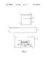
- FIG. 2illustrates the method used to acquire and display the image 13 emitted by a DNA chip 14 that is excited with ultraviolet or blue light 15 directed through an aperture 16 onto the chip.
- the emitted lightpasses through an optical filter 17 , that removes the excitation light, and impinges on the detector pixels 5 of the CMOS detector 4 .
- the CMOS detector 4contains circuitry that converts analog light impulses to digital form, which can be transmitted to a computer 8 , and ultimately displayed as a reconstructed image 18 on a monitor 11 .
- a clamping system 19holds the detector, filter, and DNA chip in contact with each other.
- a light-tight enclosure 20houses the optical system.
- An optical filteras described herein, means a light filter that blocks the passage of some wavelengths of light and allows the passage of other wavelength of light.
- FIG. 3illustrates two alternative optical detection systems for the direct mapping method.
- the DNA chipcontacts the optical filter.
- the image on the chipis directly transmitted to the CMOS detector.
- the DNA chipis in sequence with a mapping lens 3 , with focal length suitable for focusing the image emitted by the chip onto the surface of the detector.
- the theoretical resolving power of this detection methodwill be directly related to the spacing between the DNA fluorescent sources and the imaging detector pixels.
- the actual resolving powerwill also be a function of the emission from the DNA and the sophistication of the software used to extract and reconstruct the DNA fluorescence images.
- the theoretical resolving power of the configuration including a simple mapping lens or lens systemwill be limited by the optical quality of the mapping lens and by light diffraction.
- the resolving power of direct mappingcan be computed as the sum of the larger of detector pixel diameter (roughly 10 ⁇ m) or spot diameter, plus chip thickness (10 ⁇ m) plus filter thickness (10 ⁇ m).
- detector pixel diameterroughly 10 ⁇ m
- spot diameterchip thickness
- filter thickness10 ⁇ m
- a CMOS devicesuch as the HDCS-1100 (Hewlett-Packard Components Group; Corvallis, Oreg.) which has a 352 ⁇ 288 detector pixel array, can resolve approximately 1,000 spots that are 10 ⁇ m in diameter, and approximately 2,000 spots that are 50 ⁇ m in diameter.
- HDCS-1100Hewlett-Packard Components Group; Corvallis, Oreg.
- the detector pixels on suitable electronic light detector array devicescan integrate light emission with time, in much the same way that longer photographic exposure is used to develop faint images. This time integration will permit the detection of any light impulse that can be detected with a computer-assisted confocal microscope so long as the fluorescence signal exceeds device dark current and background light.
- the optical system of the invention(for example, a single mapping lens) can magnify or reduce the image.
- a mapping lenswould permit the emissions from the DNA to optimally project onto the detector pixels of the CMOS device.
- a reducing mapping lensis capable of mapping the emission from a 50 ⁇ m spot onto an individual detector pixel.
- FIG. 4is a block diagram of an embodiment of the invention.
- the light emitted from a DNA chipis passed through an optical filter and transmitted to a CMOS detector, where it is digitized, relayed to a computer, and subsequently displayed as an image on the computer's monitor.
- the inventionis compatible with laser-based visualization techniques (FIG. 5 ).
- a laser 40may be used to generate laser light 41 that may be reflected off of mirror 35 and thereby directed onto labeled DNA hybridized 30 to DNA immobilized on DNA chip 14 .
- the hybridized DNA 30fluoresces and emits fluorescent light.
- Filter 17selectively passes the fluorescent light but not the laser light 41 .
- the fluorescent lightis directly mapped onto the CCD sensor 25 .
- the lasermay be rastered across the sample so that only select portions of the sample are illuminated at one time.
- a laser-based system, or a system using a lamp-type light source 15may be used with a dichroic mirror arrangement (FIG. 6 ).
- the lamp-type source 15emits light 43 that is reflected off a dichroic mirror 36 onto immobilized, labeled, hybridized DNA 30 . If the label on the hybridized DNA 30 is a fluorescent label then the fluorescence emitted in response to excitation by light 43 may pass through dichroic mirror 36 and be mapped directly onto CCD detector 25 .
- An image on a computer screen or in a computer memorymay be generated from the detector using techniques already described.
- FIG. 6An alternative arrangement (FIG. 6) would be to create a negative image. Numerous means and combinations of making negative images will be immediately apparent to those skilled in these arts after reading this disclosure. A few examples are provided herein but are in no way intended to limit the invention.
- a negative imagecould be made by causing DNA to appear as a dark spot on a bright field. For instance a bright fluorescent field created by making DNA chip 14 with autofluorescent components, could be used with a label on hybridized DNA 30 that quenches or blocks light. The hybridized DNA would then appear as dark spots on a computer-generated image. Compounds that quench fluorescence are known to those skilled in these arts. Alternatively, hybridized DNA could be labeled after it is immobilized to the DNA chip 14 .
- a stain that blocks transmission of visible lightmay be used.
- the DNAcould already incorporate a label that could be calorimetrically developed after the DNA is immobilized; for instance, the hybridized DNA might have an enzyme that would cause a colored precipitate to form when the chip was exposed to a suitable substrate—for example, a horse radish peroxidase (HRP) system could be used.
- the immobilized DNAmight have a fluorescent molecule that was quenched by elements on the hybridizing DNA.
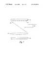
- a mapping lens 3may be used to enhance the direct mapping of the system incorporating a dichroic mirror 36 (FIG. 7 ). Mapping lens 3 will focus light that passes through dichroic mirror 36 so that the pixels of DNA on DNA chip 30 are mapped onto the detector pixels of CCD detector 25 .
- the inventionmay be embodied without an optical filter (FIGS. 8B, 8 C).
- a light-transmitting DNA chip 14 with hybridized DNAmay be treated so that the hybridized DNA appears as dark spots that fully or partially block light.
- Light 43 from a light sourcepasses though DNA chip 14 but is blocked by light-blocking hybridized DNA 32 .
- the resultant map that is formed on CCD detector 25shows the addresses that have hybridized DNA.
- Many fluorescent and non-fluorescent techniques for labeling DNA before or after its hybridization to DNA or before or after its immobilization to the DNA chip 14are known to those skilled in these arts.
- a variation on this embodimentis to place the face of DNA chip 14 that has the light-blocking DNA 32 on the side opposite the light source.
- a cover 52may be interposed between the DNA 32 and the CCD detector 25 so that CCD detector is not fouled by the DNA 32 .
- the cover 52may be a mere protective film such as a coating, or a coverslip, a plastic wrap such as polyethylene film, or other material that transmits the wavelength of the light 41 .
- Light 43may be any wavelength specified herein as light and DNA 32 may be any means for blocking that transmission that is known to those skilled in these arts.
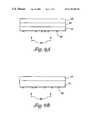
- the filters, lenses, and DNA chips of the inventionmay be used in various combinations (FIGS. 9A, 9 B).
- a lens and filtermay be combined into lens-filter 50 that is interposed between the DNA chip 14 and CCD detector 25 .
- the DNA chipmay be made as DNA chip-filter 51 that provided a solid substrate for DNA immobilization and acts to filter the light from the light source or from the immobilized DNA 30 .
- Materials or coatings for filtersare well-known to those skilled in the optical arts.
Landscapes
- Physics & Mathematics (AREA)
- General Physics & Mathematics (AREA)
- Engineering & Computer Science (AREA)
- Theoretical Computer Science (AREA)
- Investigating, Analyzing Materials By Fluorescence Or Luminescence (AREA)
- Lasers (AREA)
- Measuring Or Testing Involving Enzymes Or Micro-Organisms (AREA)
- Solid State Image Pick-Up Elements (AREA)
- Apparatus Associated With Microorganisms And Enzymes (AREA)
Abstract
Description
A DNA chip is a rigid flat surface, typically glass or silicon, with short chains of related nucleic acids spotted in rows and columns on it. Hybridization between a fluorescently-labeled DNA and specific locations on the chip can be detected and analyzed by computer-based instrumentation. The information derived from the results of hybridization to DNA chips is stimulating advances in drug development, gene discovery, gene therapy, gene expression, genetic counseling, and plant biotechnology.
Among the technologies for creating DNA chips are photolithograpy, “on-chip” synthesis, piezoelectric printing, and direct printing. Chip dimensions, the number of sites of DNA deposition (sometimes termed “addresses”) per chip, and the width of the DNA spot per “address” are dependent upon the technologies employed for deposition. The most commonly used technologies produce spots with diameters of 50-300 μm. Photolithography produces spots that can have diameters as small as 1 micron. Technologies for making such chips are known to those skilled in these arts and arc described, for instance, in U.S. Pat. Nos. 5,925,525, 5,919,523, 5,837,832, and 5,744,305, which are incorporated herein by reference.
Hybridization to DNA chips can be monitored by fluorescence optics, by radioisotope detection, and by mass spectrometry. The most widely-used method for detection of hybridization employs fluorescently-labeled DNA, and a computerized system featuring a confocal fluorescence microscope (or an epifluorescence microscope), a movable microscope stage, and DNA detection software. Technical characteristics of these microscope systems are described in U.S. Pat. Nos., 5,293,563, 5,459,325, and 5,552,928, which are incorporated herein by reference. Further descriptions of imaging fluorescently immobilized biomolecules and analysis of the images are set forth in U.S. Pat. Nos. 5,874,219, 5,871,628, 5,834,758, 5,631,734, 5,578,832, 5,552,322, and 5,556,539 which are incorporated herein by reference.
In brief, these conventional approaches to visualizing the surface of a DNA chip involve placing the chip on a microscope stage, moving the stage to put the sample into focus with a microscope objective, and triggering a digital camera or similar device to capture an image. An objective is a device made of a group of lenses that have a sophisticated design that collects light from the sample, magnifies the image of the sample, and minimizes the unavoidable image and color distortion caused by the passage of the light through the objective. The light-collected from the sample passes through the objective and through a set of mirrors and lenses until is delivered to an eyepiece or the camera. The light path is the path that the light takes from the point where it leaves the surface of the sample until it reaches an imaging device such as an eyepiece or camera. The microscopes are integral with light sources that direct light on to the sample.
These microscopes also have sets of optical filters that allow for viewing of fluorescent images. The DNA that is hybridized to the surface of the DNA chip is typically labeled with fluorescent molecules that absorb light at one wavelength and then emit a different wavelength. The microscope is equipped with sets of optical filters that block the wavelengths of light from the light source but allow the light emitted by the fluorescent molecules to pass through the light path to reach the eyepiece or camera. The light source is typically integral with the microscope and is an important part of the imaging system.
These conventional microscopes are sophisticated and expensive instruments that require training and maintenance. A single microscope objective typically has multiple lenses. A lens, as used herein, means a transparent solid material shaped to magnify, reduce, or redirect light rays. A light filter or mirror is distinct from a lens. Furthermore, use of a microscope requires a dedicated workspace that is approximately the size of a typical desk. Conventional microscopes have a light path that is several centimeters long that transmits the collected light through air and other assorted optical devices within the light path. One of the challenges in microscopy is making the microscope as efficient as possible in capturing all of the light that leaves the sample surface so that an optimal image may be made.
The costly instrumentation conventionally used to image DNA clips impedes the broad usage of DNA chip technologies.
What is needed is an inexpensive, low-maintenance alternative spot detection method for DNA chip analysis that is easy to use and requires a minimum of space and maintenance.
Integrated electronic circuit arrays for light-detection (herein referred to as members of the group of detectors called electronic light detector arrays) and analysis are readily available. They generally are based on CCD (charge-coupled device) or CMOS (complementary metal oxide semiconductor) technologies. Both CCD and CMOS imaging detectors are two-dimensional arrays of electronic light sensors. Each array consists of a set of known, unique positions that are also called addresses. Each address in a CCD or CMOS array is occupied by a sensor that covers an area that is typically shaped as a box or a rectangle; this area or the area occupied by a single sensor is referred to as a pixel. Herein, a light-detecting sensor located on a pixel is called a detector pixel. A detector pixel may be in a CCD sensor, a CMOS sensor, or other device that detects or measures light. The sizes of detector pixels vary widely and may have a diameter or length of 0.2 μm, which is the theoretical limit of resolution of the light microscope. Thus an invention that directly employs electronic detection instead of a conventional optical system is potentially as powerful as any light microscope. Light, as used herein, means any electromagnetic emission of at least 120 nm wavelength and includes ultraviolet, visible, and infrared light.
CCDs, widely used in consumer and scientific applications such as digital recorders and digital cameras, are most sensitive, and may be made with detector pixels that are smaller than those of CMOS devices. CMOS devices are now beginning to be incorporated in recorders and cameras because they are less expensive to produce. CMOS devices also are easier to interface with external control systems than CCDs. Some readily-available CMOS devices are capable of acquiring, digitizing, and transmitting an image without additional circuitry, while CCD arrays require two or more additional circuit elements to accomplish the same tasks.
The present invention describes an inexpensive device and method for resolving the light spots emitted by a light-transparent DNA chip. The method is direct mapping of the light emitted by a single DNA spot onto corresponding detector pixels of an electronic light detector array system. One method is to put the DNA chip in direct physical contact with the electronic light detector array system. In a modification of this basic method, a simple optical system, such as a single mapping lens, maps an enlarged or reduced version of the DNA array onto the electronic light detector array. Computer software processes the data from the electronic light detector array system. The data may be treated as a two-dimensional map or otherwise processed as an array.
Implementation of the described method would replace the expensive optical detection systems currently employed for DNA chip analysis with an inexpensive system. This system comprises an electronic light detector array, a filter, and, optionally, a mapping lens system. The invention enables the DNA chip to be mapped onto the electronic light detector array. Thus each position on the DNA chip surface has a corresponding position or set of positions on the detector array whereby a fluorescence at an address on the DNA chip surface is projected onto a known pixel or set of pixels.
Direct mapping is inexpensive. It eliminates the need for a complicated microscope that requires maintenance and trained personnel. It captures light directly from the sample; by eliminating many lenses, disadvantages stemming from use of many lenses are reduced. Direct mapping enables direct capture of light so that a maximal amount of light is captured from the sample; minimizing the loss of light creates a very sensitive imaging system.
Electronic light detector array systems include an electronic light detector array such as a CMOS or CCD chip and the associated equipment for visualization. This associated equipment includes filters, lenses, and light sources. The filters may be any filter used to reflect or selectively pass or reject light wavelengths. Such filters include edge filters, narrow band filters, dichroic mirrors and filters used in the visualization arts, including optical, ultraviolet, confocal, and two- or multi-photon microscopy. Light sources include those commonly used in the visualization arts, including optical, ultraviolet, confocal, and two-photon or multi-photon microscopy. Light sources further include light lamps and light lasers, such as visible-light lamps, ultraviolet lamps, mercury lamps, and lasers, including argon lasers, helium-cadmium lasers, semiconductor lasers, and so forth.
Various associated equipment is found in association with these devices, and are known to those skilled in these arts. Such equipment includes manual or electric filter-switchers, movable mirrors, and motors and controls to raster a laser across a sample. Various equipment is associated with CCD and CMOS sensors, which are incorporated into a myriad of commercially available cameras and detectors. For instance, various equipment and techniques are known for producing a color image using red, green, and blue detection; for example, an image may be split into three images, each of which is sent through a red, green, or blue filter to a CCD sensor. Or CCD sensors may be placed on a chip with different sensitivities to red, green, and blue light. Such equipment include techniques and electronic means for improving an image, and include electronic filters (high-pass, low-pass. etc.), time and frame-averaging, image subtraction, and other techniques known to those skilled in these arts.
The detection system may be configured to excite, detect, filter, and process fluorescence from conventional fluorophores, for example, fluorophores described in catalogues published by Life Technologies, Inc. (Rockville, Md.), Sigma-Aldrich, Inc. (SIGMA, ALDRICH, and FLUKA brand names; St. Louis, Mo.), Pierce Chemicals (Rockford, Ill.), and other suppliers known to those skilled in these arts. Similarly, other DNA visualization techniques are currently known and used, and many examples of these technologies are set forth in these same sources. For instance, calorimetric systems that create a color in the visible light wavelength, for instance those based on a stain or on enzyme activity, may be adapted to visualize DNA. And amplification systems that may be used in combination with a colorimetric or fluorescent system may also be used; for example, avidin-biotin or antibody-based techniques. For example, the target DNA labeled with biotin may be placed on the DNA chip. After a washing protocol is performed, the sample may be exposed to labeled avidin, which makes a strong bond to the biotin. The label on the avidin may be a fluorophore (or an enzyme such as horseradish peroxidase (HRP) that is suitable for calorimetric assay). Additionally, DNA may be labeled by chemiluminescence or chemifluorescence and subsequently detected.
DNA may be attached to substrates that pass light by a variety of means known to those skilled in these arts. For instance, glass or quartz may be treated with silanes to create carboxyl or amine groups that may be used in further chemical reactions for immobilizing DNA. Such techniques and many others known to those skilled in these arts are included in the patents incorporated by reference, above, as well as in the following references, which are incorporated herein by reference: Laursen et al., “Solid Phase Methods in Protein Sequence Analysis,” in Methods of Biochemical Analysis, vol 26 John Wiley & Sons, Inc. 1980, pp. 202-215; “Immobilization of oligonucleotides onto a glass support via disulfide bonds: A method for preparation of DNA microarrays”, Rogers Y H, Jiang-Baucom P, Huang Z J, Bogdanov V, Anderson S, Boyce-Jacino M T, Anal Biochem 1999 January 1;266(1):23-30; “Covalent attachment of DNA oligonucleotides to glass”, Cohen G, Deutsch J, Fineberg J, Levine A, Nucleic Acids Res 1997 February 15;25(4):911-2; “Hybridization of DNA targets to glass-tethered oligonucleotide probes”, Beattie W G, Meng L, Turner S L, Varma R S, Dao D D, Beattie K L, Mol Biotechnol 1995 December ;4(3):213-25; “Preparation of glass plates with cerium oxide for DNA sequencing”, Millard D, de Couet H G, Biotechniques 1995 October; 19(4):576; “Biologically Functional Materials”, Allan S. Hoffmnan, in Biomaterials Science, B. D. Ratner, A. S. Hoffmnan, F. J. Schoen, and J. E. Lemons, Eds., pp. 124-130.
The invention may be used with DNA or with other combinations of hybridizable molecules, for instance RNA-DNA or DNA-protein interactions. DNA-DNA hybridization has been used as an example but the invention includes all polynucleic acid hybridization techniques, including RNA-RNA hybridization. Polynucleic acid, as used herein, means DNA, RNA, two or more oligonucleotides or oligonucleosides, and all long or short sequences of nucleic acids. “DNA chip” or “polynucleic acid chip” as used herein refers not only to DNA sequences immnobilized on small solid substrates, but also refers to RNA, etc., and generally to a device with biomolecules immobilized to it.
The present invention is a device and method for detecting the pattern of polynucleic acid hybridization to a surface. The device includes (a) a positioning device for receiving a nucleic acid chip and keeping the chip in a sampling position, the nucleic acid chip being an object with a flat sample surface and an opposed surface that is joined to the sample surface by a thickness, with the sample surface having sequences of nucleic acids immobilized thereto, with each sequence being immobilized to a particular chip address. And, (b) an electronic light detector array, the detector array comprising detector pixels, the detector pixels being sensors located at particular detector pixel addresses, wherein the sampling position places the sample surface of the chip at a well-defined position relative to the electronic light detector array so that light leaving a chip address is substantially directed onto at least one detector pixel with an address that is correlated to the chip address.
FIG. 1 illustrates the components and general function of an electronic light detector array system;
FIG. 2 illustrates the use of direct mapping to acquire and reconstruct the light emitted by a DNA chip;
FIGS. 3A,3B illustrates two alternative arrangements of optical components for direct mapping;
FIG. 4 is a block diagram of an embodiment of the invention;
FIG. 5 illustrates an embodiment of the invention with a laser-light source;
FIG. 6 illustrates an embodiment of the invention with a dichroic mirror;
FIG. 7 illustrates an embodiment of the invention with a dichroic mirror and a mapping lens;
FIG. 8A illustrates a DNA chip with hybridized DNA;
FIG. 8B illustrates an embodiment of the invention with no optical filter;
FIG. 8C illustrates an embodiment of the invention with a cover-filter and no optical filter;
FIG. 9A illustrates an embodiment of the invention with a combination mapping lens-filter; and
FIG. 9B illustrates an embodiment of the invention with a combination chip-filter.
Electronic direct mapping is analogous to the established photographic method known as contact printing. In contact printing, a photographic negative is placed in direct contact with unexposed photographic paper, and illuminated briefly. When the photographic paper is subsequently developed, its image has a 1:1 correspondence to the negative.
The smallest diameter DNA spot currently attainable on a DNA chip approximates the diameter or length of each detector pixel in a conventional CMOS device, roughly 10 μm. Therefore, if the DNA array and the CMOS array are in close proximity to each other, the light emitted by each member of a DNA array can be directly mapped to a limited number of detector pixels in the sensor array. This direct mapping method would eliminate the expensive optical systems that are required for DNA chip analysis, and, by lowering the cost, expand the potential applications of DNA chip technology.
FIG. 1 illustrates the electronic components and general function of an electronic light detector array detection system such as a CMOS-based detection system1 which is used to acquire and display a visual image2. The light image is collected by amapping lens 3, which focuses the image onto theCMOS detector 4. The detector containingmany detector pixels 5, is mounted on acircuit board 6, which contains a direct current power supply7 for the detector. The detector has electronic circuitry that converts the electrical signals detected by its detector pixels to digital form, and facilitates the transfer of the digitized signal to acomputer 8 via a communications cable9. In the computer, the digital signal is mapped to the computer's video memory, passed by a cable10 to amonitor 11, which displays thereconstructed image 12.
FIG. 2 illustrates the method used to acquire and display theimage 13 emitted by aDNA chip 14 that is excited with ultraviolet or blue light15 directed through anaperture 16 onto the chip. The emitted light passes through anoptical filter 17, that removes the excitation light, and impinges on thedetector pixels 5 of theCMOS detector 4. TheCMOS detector 4 contains circuitry that converts analog light impulses to digital form, which can be transmitted to acomputer 8, and ultimately displayed as areconstructed image 18 on amonitor 11. Aclamping system 19 holds the detector, filter, and DNA chip in contact with each other. A light-tight enclosure 20 houses the optical system. An optical filter, as described herein, means a light filter that blocks the passage of some wavelengths of light and allows the passage of other wavelength of light.
FIG. 3 illustrates two alternative optical detection systems for the direct mapping method. In FIG. 3A, the DNA chip contacts the optical filter. The image on the chip is directly transmitted to the CMOS detector. In FIG. 3B the DNA chip is in sequence with amapping lens 3, with focal length suitable for focusing the image emitted by the chip onto the surface of the detector.
The theoretical resolving power of this detection method will be directly related to the spacing between the DNA fluorescent sources and the imaging detector pixels. The actual resolving power will also be a function of the emission from the DNA and the sophistication of the software used to extract and reconstruct the DNA fluorescence images. The theoretical resolving power of the configuration including a simple mapping lens or lens system will be limited by the optical quality of the mapping lens and by light diffraction.
However, it is not the goal of this system to have high cost and resolution imaging optics since low cost optics with suitable software will readily map arrays of DNA pixels.
The resolving power of direct mapping can be computed as the sum of the larger of detector pixel diameter (roughly 10 μm) or spot diameter, plus chip thickness (10 μm) plus filter thickness (10 μm). Thus, the image from a 10 μm DNA spot would map onto a 30 μm×30 μm area of the detector containing 9 detector pixels, while the image from a 50 μm DNA spot would map onto a 70 μm×70 μm area countering 49 detector pixels. A CMOS device such as the HDCS-1100 (Hewlett-Packard Components Group; Corvallis, Oreg.) which has a 352×288 detector pixel array, can resolve approximately 1,000 spots that are 10 μm in diameter, and approximately 2,000 spots that are 50 μm in diameter.
The detector pixels on suitable electronic light detector array devices can integrate light emission with time, in much the same way that longer photographic exposure is used to develop faint images. This time integration will permit the detection of any light impulse that can be detected with a computer-assisted confocal microscope so long as the fluorescence signal exceeds device dark current and background light. The optical system of the invention (for example, a single mapping lens) can magnify or reduce the image. A mapping lens would permit the emissions from the DNA to optimally project onto the detector pixels of the CMOS device. For instance, a reducing mapping lens is capable of mapping the emission from a 50 μm spot onto an individual detector pixel.
FIG. 4 is a block diagram of an embodiment of the invention. The light emitted from a DNA chip is passed through an optical filter and transmitted to a CMOS detector, where it is digitized, relayed to a computer, and subsequently displayed as an image on the computer's monitor.
The invention is compatible with laser-based visualization techniques (FIG.5). For instance, alaser 40 may be used to generatelaser light 41 that may be reflected off ofmirror 35 and thereby directed onto labeled DNA hybridized30 to DNA immobilized onDNA chip 14. When incorporating a fluorescent label, the hybridizedDNA 30 fluoresces and emits fluorescent light.Filter 17 selectively passes the fluorescent light but not thelaser light 41. The fluorescent light is directly mapped onto theCCD sensor 25. The laser may be rastered across the sample so that only select portions of the sample are illuminated at one time.
A laser-based system, or a system using a lamp-type light source 15 may be used with a dichroic mirror arrangement (FIG.6). The lamp-type source 15 emits light43 that is reflected off adichroic mirror 36 onto immobilized, labeled, hybridizedDNA 30. If the label on the hybridizedDNA 30 is a fluorescent label then the fluorescence emitted in response to excitation by light43 may pass throughdichroic mirror 36 and be mapped directly ontoCCD detector 25. An image on a computer screen or in a computer memory may be generated from the detector using techniques already described.
An alternative arrangement (FIG. 6) would be to create a negative image. Numerous means and combinations of making negative images will be immediately apparent to those skilled in these arts after reading this disclosure. A few examples are provided herein but are in no way intended to limit the invention. A negative image could be made by causing DNA to appear as a dark spot on a bright field. For instance a bright fluorescent field created by makingDNA chip 14 with autofluorescent components, could be used with a label on hybridizedDNA 30 that quenches or blocks light. The hybridized DNA would then appear as dark spots on a computer-generated image. Compounds that quench fluorescence are known to those skilled in these arts. Alternatively, hybridized DNA could be labeled after it is immobilized to theDNA chip 14. For instance, a stain that blocks transmission of visible light may be used. Or the DNA could already incorporate a label that could be calorimetrically developed after the DNA is immobilized; for instance, the hybridized DNA might have an enzyme that would cause a colored precipitate to form when the chip was exposed to a suitable substrate—for example, a horse radish peroxidase (HRP) system could be used. Or the immobilized DNA might have a fluorescent molecule that was quenched by elements on the hybridizing DNA.
Amapping lens 3 may be used to enhance the direct mapping of the system incorporating a dichroic mirror36 (FIG.7).Mapping lens 3 will focus light that passes throughdichroic mirror 36 so that the pixels of DNA onDNA chip 30 are mapped onto the detector pixels ofCCD detector 25.
The invention may be embodied without an optical filter (FIGS. 8B,8C). A light-transmittingDNA chip 14 with hybridized DNA may be treated so that the hybridized DNA appears as dark spots that fully or partially block light.Light 43 from a light source passes thoughDNA chip 14 but is blocked by light-blocking hybridizedDNA 32. The resultant map that is formed onCCD detector 25 shows the addresses that have hybridized DNA. Many fluorescent and non-fluorescent techniques for labeling DNA before or after its hybridization to DNA or before or after its immobilization to theDNA chip 14 are known to those skilled in these arts. A variation on this embodiment is to place the face ofDNA chip 14 that has the light-blockingDNA 32 on the side opposite the light source. Acover 52 may be interposed between theDNA 32 and theCCD detector 25 so that CCD detector is not fouled by theDNA 32. Thecover 52 may be a mere protective film such as a coating, or a coverslip, a plastic wrap such as polyethylene film, or other material that transmits the wavelength of the light41.Light 43 may be any wavelength specified herein as light andDNA 32 may be any means for blocking that transmission that is known to those skilled in these arts.
The filters, lenses, and DNA chips of the invention may be used in various combinations (FIGS. 9A,9B). For instance a lens and filter may be combined into lens-filter 50 that is interposed between theDNA chip 14 andCCD detector 25. Or the DNA chip may be made as DNA chip-filter 51 that provided a solid substrate for DNA immobilization and acts to filter the light from the light source or from the immobilizedDNA 30. Materials or coatings for filters are well-known to those skilled in the optical arts.
Several embodiments of the invention are described herein. These embodiments are illustrative of the invention but are not to be construed as embracing all of its embodiments or as limiting on the scope of the invention.
Claims (86)
1. A device for detecting the pattern of polynucleic acid hybridization to a surface, the device comprising:
(a) a nucleic acid chip holder configured to receive a nucleic acid chip and keep the chip in a sampling position;
the nucleic acid chip being an object with a flat sample surface and an opposed surface that is joined to the sample surface by a thickness, with the sample surface having sequences of nucleic acids immobilized thereto, with each sequence being immobilized to a particular chip address;
(b) an optical filter that selectively transmits light;
(c) an electronic light detector array, the detector array comprising detector pixels, the detector pixels being sensors located at particular detector pixel addresses; and
(d) a light source that generates source light wherein the sampling position is a position that places the sample surface of the chip in a well-defined spatial relationship relative to the electronic light detector array so that the source light that touches a chip address on the sample surface is substantially directed onto at least one detector pixel with an address that is correlated to the chip address.
2. The device ofclaim 1 wherein the chip address to the detector pixel correlation is one-to-one, whereby the light to aching a single chip address is directed to substantially one detector pixel.
3. The device ofclaim 1 wherein more than one detector pixel is correlated to one chip address.
4. The device ofclaim 1 wherein light leaving the sample surface of the chip passes through the chip thickness before reaching the detector pixels.
5. The device ofclaim 4 wherein the light leaving the sample surface of the chip passes through an optical filter.
6. The device ofclaim 5 comprising a mapping lens that changes the direction of light rays leaving the sample surface of the chip, wherein the mapping lens is located between the sample surface and the detector pixels.
7. The device ofclaim 6 wherein the mapping lens is a reducing lens.
8. The device ofclaim 6 wherein the mapping lens is a magnifying lens.
9. The device ofclaim 6 wherein the mapping lens comprises a light collimator.
10. The device ofclaim 6 wherein the mapping lens and the optical filter are combined into one apparatus.
11. The device ofclaim 6 wherein the chip further comprises the mapping lens.
12. The device ofclaim 11 wherein the bottom surface of the chip comprises a curved surface that functions as the mapping lens.
13. The device ofclaim 5 wherein the chip is in direct physical contact with the filter.
14. The device ofclaim 13 wherein the bottom surface of the chip is in contact with the filter.
15. The device ofclaim 14 wherein the filter and the detector array are in direct physical contact.
16. The device ofclaim 5 wherein the bottom surface of the chip is in direct physical contact with the filter.
17. The device ofclaim 4 wherein the nucleic acids are DNA.
18. The device ofclaim 4 wherein the chip is made of quartz.
19. The device ofclaim 4 wherein the chip is made of glass.
20. The device ofclaim 4 wherein the chip is made of light-transmissive plastic.
21. The device ofclaim 20 wherein the plastic is polystyrene.
22. The device ofclaim 4 comprising the chip, wherein the chip comprises an optical filter.
23. The device ofclaim 22 wherein the chip bottom surface is coated with an optical coating.
24. The device ofclaim 23 wherein the chip is in direct physical contact with the electronic light detector array.
25. The device ofclaim 4 wherein the detector array detector pixels are in direct physical contact with the optical filter.
26. The device ofclaim 25 wherein all of the detector array detector pixels are in direct physical contact with the optical filter.
27. A device for detecting the pattern of polynucleic acid hybridization to a surface, the device comprising:
(a) a nucleic acid chip holder configured to receive a nucleic acid chip and keep the chip in a sampling position;
the nucleic acid chip being an object with a flat sample surface and an opposed surface that is joined to the sample surface by a thickness, with the sample surface having sequences of nucleic acids immobilized thereto, with each sequence being immobilized to a particular chip address; and
(b) an electronic light detector array, the detector array comprising detector pixels, the detector pixels being sensors located at particular detector pixel addresses;
wherein the sampling position places the sample surface of the chip at a well-defined position relative to the electronic light detector array so that source light from a light source that touches a chip address on the sample surface is substantially directed onto at least one detector pixel with an address that is correlated to the chip address.
28. The device ofclaim 27 wherein the chip address to the detector pixel correlation is one-to-one.
29. The device ofclaim 27 wherein more than one detector pixel is correlated to one chip address.
30. The device ofclaim 27 wherein light leaving the sample surface of the chip passes through the chip thickness before reaching the detector pixels.
31. The device ofclaim 27 wherein the light leaving the sample surface of the chip passes through an optical filter.
32. The device ofclaim 31 wherein the optical filter allows substantially only light generated at the sample surface to pass to the detector.
33. The device ofclaim 32 wherein the optical filter substantially blocks the source light.
34. The device ofclaim 27 wherein the chip and the detector array are in direct physical contact.
35. The device ofclaim 34 wherein all wavelengths of light that touch the sample surface of the DNA chip are allowed to pass to the detector array.
36. The device ofclaim 35 wherein no optical filter is used in the light path between the sample surface and the detector array.
37. The device ofclaim 35 wherein all wavelengths of the source light are allowed to reach the detector pixels.
38. The device ofclaim 34 wherein the chip comprises an optical filter.
39. The device ofclaim 34 wherein the chip further comprises a mapping lens.
40. The device ofclaim 27 wherein the position of a dark spot on the sample surface, the dark spot being a spot that substantially blocks the passage of light, is mapped directly onto the detector array.
41. The device ofclaim 27 wherein the light source is used to illuminate the sample surface so that light leaving the sample surface is projected onto the detector array so that a dark spot on the sample surface, the dark spot being a spot on the sample surface that blocks more light than the surrounding surface, causes less light to be received by at least one detector pixel, whereby the address of the dark spot on the sample surface is detected.
42. A device for detecting the pattern of polynucleic acid hybridization to a surface, the device comprising:
(a) a nucleic acid chip holder configured to receive a nucleic acid chip and keep the chip in a sampling position;
the nucleic acid chip being an object with a flat sample surface and an opposed surface that is joined to the sample surface by a thickness, with the sample surface having sequences of nucleic acids immobilized thereto, with each sequence being immobilized to a particular chip address; and
(b) an electronic light detector array, the detector array comprising detector pixels, the detector pixels being sensors located at particular detector pixel addresses;
wherein the sampling position places the sample surface of the chip at a well-defined position relative to the electronic light detector array so that light leaving a chip address is substantially directed onto at least one detector pixel with an address that is correlated to the chip address.
43. The device ofclaim 42 wherein the chip address to the detector pixel correlation is one-to-one.
44. The device ofclaim 42 wherein more than one detector pixel is correlated to one chip address.
45. The device ofclaim 42 further including at least one optical lens, the optical lens being used to map an image of the sample surface onto the electronic light detector array.
46. The device ofclaim 45 wherein the number of all optical lenses used to map an image of the sample surface onto the electronic light detector array is one.
47. The device ofclaim 45 wherein the number of all optical lenses used to map an image of the sample surface onto the electronic light detector array is two.
48. The device ofclaim 42 wherein light leaving the sample surface of the chip is generated by chemiluminescence.
49. The device ofclaim 42 wherein light leaving the sample surface of the chip is generated by fluorescence.
50. The device ofclaim 42 wherein light leaving the sample surface of the chip is generated by two-photon excitation.
51. The device ofclaim 42 wherein light leaving the sample surface of the chip is generated by multi-photon excitation.
52. The device ofclaim 42 wherein the light leaving the sample surface is generated by fluorescence and polynucleic acids that attach to the sample surface cause a quenching of fluorescence.
53. The device ofclaim 52 wherein the light leaving the sample surface is generated by fluorescence and polynucleic acids that attach to the sample surface have attached molecules that cause a quenching of fluorescence.
54. The device ofclaim 42 wherein light leaving the sample surface of the chip is generated by a light source that generates source light.
55. The device ofclaim 54 wherein the source light is light that is detectable by the human eye.
56. The device ofclaim 42 wherein the light leaving the sample surface is generated by a light source that generates source light and polynucleic acides that attach to the sample surface have attached molecules that cause a decrease of the intensity of the light that leaves the sample surface.
57. The device ofclaim 42 wherein the light leaving the sample surface of the chip passes through an optical filter.
58. The device ofclaim 57 wherein the optical filter allows substantially only light generated at the sample surface to pass to the detector.
59. The device ofclaim 58 wherein the optical filter substantially blocks the light that is not generated at the sample surface.
60. The device ofclaim 42 wherein the chip and the detector array are in direct physical contact.
61. The device ofclaim 42 wherein light leaving the sample surface of the chip passes through the chip thickness before reaching the detector pixels.
62. The device ofclaim 42 wherein all wavelengths of light that touch the sample surface of the DNA chip are allowed to pass to the detector array.
63. The device ofclaim 62 wherein no optical filter is used in the light path between the sample surface and the detector array.
64. The device ofclaim 62 wherein all wavelengths of the source light are allowed to reach the detector pixels.
65. The device ofclaim 64 wherein the length of the light path is between 15 microns and 1 centimeter.
66. A system for imaging spots of polynucleic acid on a polynucleic acid chip, the system comprising:
(a) light source means that emits source light;
(b) light detector means, the light detector means including detector pixels;
(c) holding means for holding the chip, the chip comprising a top sample surface and a bottom, the sample surface having addresses, the holding means being positioned relative to the light detector means so that light leaving a sample surface address is mapped onto at least one detector pixel;
(d) electronic data processing means that processes electronic data from the chip;
(e) data transmitting means that transmits data from the electronic light detector array
(f) the system having a sample light path, which is the light path that must be to the electronic data processing means; and
traveled by all of the light that leaves the sample surface and is detectable by the light detector means.
67. The system ofclaim 66 wherein the sample light path is less than 15 microns.
68. The system ofclaim 66 wherein every point of the sample light path has an index of refraction that is greater than 1.0.
69. The system ofclaim 68 wherein the sample light path is comprised of solid materials.
70. The system ofclaim 66 wherein the sample light path does not include an optical lens that magnifies the image of the sample surface.
71. The system ofclaim 66 wherein the sample light path does not include an optical lens that reduces the image of the sample surface.
72. The system ofclaim 66 wherein the sample light path is less than 1 centimeter.
73. The system ofclaim 66 wherein the sample light path is less than one millimeter.
74. The system ofclaim 66 wherein the sample light path is less than 200 microns.
75. The system ofclaim 66 wherein the sample light path is less than 75 microns.
76. The system ofclaim 66 wherein the sample light path is less than 35 microns.
77. A method for detecting spots of polynucleic acid on a polynucleic acid chip, the method comprising the following steps:
(a) loading a polynucleic acid chip in a holder,
(b) positioning the holder at a sampling position, the sampling position being a position relative to a light detector that establishes a sampling distance between the top sample surface of the chip and the light detector that allows light that emanates from a point approximately at the surface of the chip to travel along a short light path to the light detector, and
(c) using a detection means to detect the signal generated by the light detector.
78. The method ofclaim 77 wherein the short light path is less than four millimeters.
79. The method ofclaim 77 wherein the short light path is less than 200 microns.
80. The method ofclaim 77 wherein the light path is substantially linear.
81. The method ofclaim 78 comprising the steps of using a positioning means to bring the holder from a loading position to the sampling position.
82. The method ofclaim 81 wherein the positioning means comprises a sliding mechanism.
83. The method ofclaim 82 wherein the positioning means comprises a motor.
84. The method ofclaim 83 wherein a chip is loaded into the holder while the holder is in a loading position and a switch is activated to turn the motor on to slide the holder to the sampling position.
85. The method ofclaim 77 further comprising focusing steps, the focusing steps comprising:
(i) moving the holder to a new position,
(ii) using the light detector, the detection means, and a graphic display means to visualize the surface of the sample; and
(iii) repeating steps (i) and (ii) until a sampling distance desired by a user is achieved.
86. The method ofclaim 85 wherein the focusing steps are automatically performed by a programmable computer.
Priority Applications (9)
| Application Number | Priority Date | Filing Date | Title |
|---|---|---|---|
| US09/434,027US6784982B1 (en) | 1999-11-04 | 1999-11-04 | Direct mapping of DNA chips to detector arrays |
| CA002388034ACA2388034A1 (en) | 1999-11-04 | 2000-11-02 | Direct mapping of dna chips to detector arrays |
| PCT/US2000/041799WO2001034846A2 (en) | 1999-11-04 | 2000-11-02 | Direct mapping of dna chips to detector arrays |
| EP00991918AEP1228248A2 (en) | 1999-11-04 | 2000-11-02 | Direct mapping of dna chips to detector arrays |
| AU36403/01AAU3640301A (en) | 1999-11-04 | 2000-11-02 | Direct mapping of dna chips to detector arrays |
| JP2001536771AJP2003515107A (en) | 1999-11-04 | 2000-11-02 | Direct mapping of DNA chips to detector arrays |
| US09/852,375US7145645B2 (en) | 1999-11-04 | 2001-05-10 | Imaging of biological samples using electronic light detector |
| US10/211,113US6867851B2 (en) | 1999-11-04 | 2002-08-02 | Scanning of biological samples |
| US11/566,594US20070121111A1 (en) | 1999-11-04 | 2006-12-04 | Imaging of Biological Samples |
Applications Claiming Priority (1)
| Application Number | Priority Date | Filing Date | Title |
|---|---|---|---|
| US09/434,027US6784982B1 (en) | 1999-11-04 | 1999-11-04 | Direct mapping of DNA chips to detector arrays |
Related Child Applications (2)
| Application Number | Title | Priority Date | Filing Date |
|---|---|---|---|
| US09/852,375Continuation-In-PartUS7145645B2 (en) | 1999-11-04 | 2001-05-10 | Imaging of biological samples using electronic light detector |
| US11/566,594Continuation-In-PartUS20070121111A1 (en) | 1999-11-04 | 2006-12-04 | Imaging of Biological Samples |
Publications (1)
| Publication Number | Publication Date |
|---|---|
| US6784982B1true US6784982B1 (en) | 2004-08-31 |
Family
ID=23722513
Family Applications (3)
| Application Number | Title | Priority Date | Filing Date |
|---|---|---|---|
| US09/434,027Expired - LifetimeUS6784982B1 (en) | 1999-11-04 | 1999-11-04 | Direct mapping of DNA chips to detector arrays |
| US09/852,375Expired - LifetimeUS7145645B2 (en) | 1999-11-04 | 2001-05-10 | Imaging of biological samples using electronic light detector |
| US11/566,594AbandonedUS20070121111A1 (en) | 1999-11-04 | 2006-12-04 | Imaging of Biological Samples |
Family Applications After (2)
| Application Number | Title | Priority Date | Filing Date |
|---|---|---|---|
| US09/852,375Expired - LifetimeUS7145645B2 (en) | 1999-11-04 | 2001-05-10 | Imaging of biological samples using electronic light detector |
| US11/566,594AbandonedUS20070121111A1 (en) | 1999-11-04 | 2006-12-04 | Imaging of Biological Samples |
Country Status (6)
| Country | Link |
|---|---|
| US (3) | US6784982B1 (en) |
| EP (1) | EP1228248A2 (en) |
| JP (1) | JP2003515107A (en) |
| AU (1) | AU3640301A (en) |
| CA (1) | CA2388034A1 (en) |
| WO (1) | WO2001034846A2 (en) |
Cited By (40)
| Publication number | Priority date | Publication date | Assignee | Title |
|---|---|---|---|---|
| US20030175987A1 (en)* | 2002-03-18 | 2003-09-18 | Edward Verdonk | Biochemical assay with programmable array detection |
| US20040008867A1 (en)* | 2001-07-06 | 2004-01-15 | Howard Fein | Imaging system, methodology, and applications employing reciprocal space optical design |
| US20040071599A1 (en)* | 2002-03-22 | 2004-04-15 | Rusch Terry L. | Apparatus and method for testing and continuously reading low-volume samples |
| US20040165778A1 (en)* | 2001-07-06 | 2004-08-26 | Cartlidge Andrew G. | Semiconductor imaging system methodology |
| US20040246479A1 (en)* | 2001-07-06 | 2004-12-09 | Cartlidge Andrew G. | Particle analyzing system and methodology |
| US20070036511A1 (en)* | 2005-08-11 | 2007-02-15 | Pacific Biosciences Of California, Inc. | Methods and systems for monitoring multiple optical signals from a single source |
| US20070097364A1 (en)* | 2005-05-09 | 2007-05-03 | The Trustees Of Columbia University In The City Of New York | Active CMOS biosensor chip for fluorescent-based detection |
| US20070188750A1 (en)* | 2006-02-13 | 2007-08-16 | Pacific Biosciences Of California, Inc. | Methods and systems for simultaneous real-time monitoring of optical signals from multiple sources |
| US20070206187A1 (en)* | 2006-02-13 | 2007-09-06 | Pacific Biosciences Of California, Inc. | Methods and systems for simultaneous real-time monitoring of optical signals from multiple sources |
| US7297553B2 (en) | 2002-05-28 | 2007-11-20 | Nanosphere, Inc. | Method for attachment of silylated molecules to glass surfaces |
| US20080030628A1 (en)* | 2006-02-13 | 2008-02-07 | Pacific Biosciences Of California, Inc. | Methods and systems for simultaneous real-time monitoring of optical signals from multiple sources |
| US20080037008A1 (en)* | 2005-05-09 | 2008-02-14 | Shepard Kenneth L | Active CMOS biosensor chip for fluorescent-based detection |
| US20080080059A1 (en)* | 2006-09-28 | 2008-04-03 | Pacific Biosciences Of California, Inc. | Modular optical components and systems incorporating same |
| US20080128627A1 (en)* | 2006-09-01 | 2008-06-05 | Pacific Biosciences Of California, Inc. | Substrates, systems and methods for analyzing materials |
| US20080277595A1 (en)* | 2007-05-10 | 2008-11-13 | Pacific Biosciences Of California, Inc. | Highly multiplexed confocal detection systems and methods of using same |
| US20090075838A1 (en)* | 2002-09-16 | 2009-03-19 | The Board Of Trustees Of The Leland Stanford Junior University | Biological Analysis Arrangement and Approach Therefor |
| US20090082214A1 (en)* | 2001-03-09 | 2009-03-26 | Apollo Biotechnology, Inc. | Conjugate probes and optical detection of analytes |
| US20100065726A1 (en)* | 2006-09-01 | 2010-03-18 | Pacific Biosciences Of California, Inc. | Substrates and optical systems and methods of use thereof |
| US7687437B2 (en) | 2001-07-13 | 2010-03-30 | Nanosphere, Inc. | Method for immobilizing molecules onto surfaces |
| US20100167413A1 (en)* | 2007-05-10 | 2010-07-01 | Paul Lundquist | Methods and systems for analyzing fluorescent materials with reduced autofluorescence |
| US8207509B2 (en) | 2006-09-01 | 2012-06-26 | Pacific Biosciences Of California, Inc. | Substrates, systems and methods for analyzing materials |
| US8465699B2 (en) | 2010-02-19 | 2013-06-18 | Pacific Biosciences Of California, Inc. | Illumination of integrated analytical systems |
| CN103604784A (en)* | 2013-11-05 | 2014-02-26 | 浙江工业大学 | CMOS (Complementary Metal-Oxide-Semiconductor Transistor) contact type fluorescent homogeneous assay array sensing chip |
| US8906320B1 (en) | 2012-04-16 | 2014-12-09 | Illumina, Inc. | Biosensors for biological or chemical analysis and systems and methods for same |
| US8994946B2 (en) | 2010-02-19 | 2015-03-31 | Pacific Biosciences Of California, Inc. | Integrated analytical system and method |
| US9041790B2 (en) | 2009-10-28 | 2015-05-26 | Alentic Microscience Inc. | Microscopy imaging |
| US9075225B2 (en) | 2009-10-28 | 2015-07-07 | Alentic Microscience Inc. | Microscopy imaging |
| US9223084B2 (en) | 2012-12-18 | 2015-12-29 | Pacific Biosciences Of California, Inc. | Illumination of optical analytical devices |
| US9372308B1 (en) | 2012-06-17 | 2016-06-21 | Pacific Biosciences Of California, Inc. | Arrays of integrated analytical devices and methods for production |
| US9606068B2 (en) | 2014-08-27 | 2017-03-28 | Pacific Biosciences Of California, Inc. | Arrays of integrated analytical devices |
| US9624540B2 (en) | 2013-02-22 | 2017-04-18 | Pacific Biosciences Of California, Inc. | Integrated illumination of optical analytical devices |
| CN106770131A (en)* | 2017-01-17 | 2017-05-31 | 清华大学 | Three-dimensional ultraphotic composes micro imaging system and imaging method |
| US9989750B2 (en) | 2013-06-26 | 2018-06-05 | Alentic Microscience Inc. | Sample processing improvements for microscopy |
| US10254225B2 (en) | 2013-12-10 | 2019-04-09 | Illumina, Inc. | Biosensors for biological or chemical analysis and methods of manufacturing the same |
| US10365434B2 (en) | 2015-06-12 | 2019-07-30 | Pacific Biosciences Of California, Inc. | Integrated target waveguide devices and systems for optical coupling |
| US10487356B2 (en) | 2015-03-16 | 2019-11-26 | Pacific Biosciences Of California, Inc. | Integrated devices and systems for free-space optical coupling |
| US10502666B2 (en) | 2013-02-06 | 2019-12-10 | Alentic Microscience Inc. | Sample processing improvements for quantitative microscopy |
| US10861829B2 (en) | 2017-12-26 | 2020-12-08 | Illumina, Inc. | Sensor system |
| US11983790B2 (en) | 2015-05-07 | 2024-05-14 | Pacific Biosciences Of California, Inc. | Multiprocessor pipeline architecture |
| US12022236B2 (en) | 2009-10-28 | 2024-06-25 | Alentic Microscience Inc. | Detecting and using light representative of a sample |
Families Citing this family (99)
| Publication number | Priority date | Publication date | Assignee | Title |
|---|---|---|---|---|
| US5631734A (en) | 1994-02-10 | 1997-05-20 | Affymetrix, Inc. | Method and apparatus for detection of fluorescently labeled materials |
| CN1500140A (en)* | 2001-03-28 | 2004-05-26 | 上海晶泰生物技术有限公司 | Device and method for measuring a great variety of matters to be analyzed |
| JP2003014741A (en)* | 2001-05-25 | 2003-01-15 | Akihiro Fujimura | Method of manufacturing mosaic reagent, and so on, and its product and manufacturing device |
| EP1345026B1 (en) | 2002-03-15 | 2010-05-05 | Affymetrix, Inc. | System and method for scanning of biological materials |
| US7154598B2 (en) | 2002-07-12 | 2006-12-26 | Decision Biomarkers, Inc. | Excitation and imaging of fluorescent arrays |
| US20060127946A1 (en)* | 2002-08-16 | 2006-06-15 | Montagu Jean I | Reading of fluorescent arrays |
| US7384742B2 (en)* | 2002-08-16 | 2008-06-10 | Decision Biomarkers, Inc. | Substrates for isolating reacting and microscopically analyzing materials |
| ES2279068T3 (en)* | 2002-10-10 | 2007-08-16 | Illinois Tool Works Inc. | SAMPLE TEST |
| AU2003297588A1 (en)* | 2002-12-02 | 2004-06-23 | 3M Innovative Properties Company | Illumination system using a plurality of light sources |
| WO2004059006A1 (en)* | 2002-12-25 | 2004-07-15 | Casio Computer Co., Ltd. | Optical dna sensor, dna reading apparatus, identification method of dna and manufacturing method of optical dna sensor |
| AU2003900924A0 (en) | 2003-02-28 | 2003-03-13 | Medsaic Pty Ltd | Imaging device |
| US7317415B2 (en) | 2003-08-08 | 2008-01-08 | Affymetrix, Inc. | System, method, and product for scanning of biological materials employing dual analog integrators |
| US20050116942A1 (en)* | 2003-09-26 | 2005-06-02 | Vander Jagt Peter G. | Color measurement instrument |
| US7250611B2 (en)* | 2003-12-02 | 2007-07-31 | 3M Innovative Properties Company | LED curing apparatus and method |
| US20050116635A1 (en)* | 2003-12-02 | 2005-06-02 | Walson James E. | Multiple LED source and method for assembling same |
| US7403680B2 (en)* | 2003-12-02 | 2008-07-22 | 3M Innovative Properties Company | Reflective light coupler |
| US7329887B2 (en)* | 2003-12-02 | 2008-02-12 | 3M Innovative Properties Company | Solid state light device |
| US20050116235A1 (en)* | 2003-12-02 | 2005-06-02 | Schultz John C. | Illumination assembly |
| US7456805B2 (en) | 2003-12-18 | 2008-11-25 | 3M Innovative Properties Company | Display including a solid state light device and method using same |
| US20050221351A1 (en)* | 2004-04-06 | 2005-10-06 | Affymetrix, Inc. | Methods and devices for microarray image analysis |
| US7939022B2 (en)* | 2004-08-05 | 2011-05-10 | Avago Technologies General Ip (Singapore) Pte. Ltd. | Integration of colorimetric transducers and detector |
| US20060054801A1 (en)* | 2004-08-25 | 2006-03-16 | Long-Song Cheng | Biochip scanning device |
| US7585664B2 (en)* | 2004-10-14 | 2009-09-08 | The Hong Kong University Of Science And Technology | Integrated circuit optical detector for biological detection |
| US20070023643A1 (en) | 2005-02-01 | 2007-02-01 | Nolte David D | Differentially encoded biological analyzer planar array apparatus and methods |
| US7405831B2 (en) | 2005-02-01 | 2008-07-29 | Purdue Research Foundation | Laser scanning interferometric surface metrology |
| US7910356B2 (en) | 2005-02-01 | 2011-03-22 | Purdue Research Foundation | Multiplexed biological analyzer planar array apparatus and methods |
| US8351026B2 (en) | 2005-04-22 | 2013-01-08 | Affymetrix, Inc. | Methods and devices for reading microarrays |
| US20060252070A1 (en)* | 2005-04-28 | 2006-11-09 | Applera Corporation | Multi-Color Light Detection With Imaging Detectors |
| US7991242B2 (en) | 2005-05-11 | 2011-08-02 | Optosecurity Inc. | Apparatus, method and system for screening receptacles and persons, having image distortion correction functionality |
| US20070041613A1 (en)* | 2005-05-11 | 2007-02-22 | Luc Perron | Database of target objects suitable for use in screening receptacles or people and method and apparatus for generating same |
| EP1886257A1 (en)* | 2005-05-11 | 2008-02-13 | Optosecurity Inc. | Method and system for screening luggage items, cargo containers or persons |
| WO2007014188A2 (en)* | 2005-07-25 | 2007-02-01 | Duke University | Methods, systems, and computer program products for optimization of probes for spectroscopic measurement in turbid media |
| US8320650B2 (en)* | 2005-11-30 | 2012-11-27 | Lawrence Livermore National Security, Llc | In vivo spectral micro-imaging of tissue |
| US9445025B2 (en) | 2006-01-27 | 2016-09-13 | Affymetrix, Inc. | System, method, and product for imaging probe arrays with small feature sizes |
| US8055098B2 (en) | 2006-01-27 | 2011-11-08 | Affymetrix, Inc. | System, method, and product for imaging probe arrays with small feature sizes |
| WO2007109126A2 (en)* | 2006-03-17 | 2007-09-27 | Duke University | Monte carlo based model of fluorescence |
| WO2007126827A2 (en)* | 2006-03-30 | 2007-11-08 | Duke University | Optical assay system for intraoperative assessment of tumor margins |
| CA2584683A1 (en)* | 2006-04-20 | 2007-10-20 | Optosecurity Inc. | Apparatus, method and system for screening receptacles and persons |
| JP2007298380A (en)* | 2006-04-28 | 2007-11-15 | Hamamatsu Photonics Kk | Sample holding member |
| US7899232B2 (en)* | 2006-05-11 | 2011-03-01 | Optosecurity Inc. | Method and apparatus for providing threat image projection (TIP) in a luggage screening system, and luggage screening system implementing same |
| US8637436B2 (en) | 2006-08-24 | 2014-01-28 | California Institute Of Technology | Integrated semiconductor bioarray |
| US11001881B2 (en) | 2006-08-24 | 2021-05-11 | California Institute Of Technology | Methods for detecting analytes |
| US8494210B2 (en)* | 2007-03-30 | 2013-07-23 | Optosecurity Inc. | User interface for use in security screening providing image enhancement capabilities and apparatus for implementing same |
| US7803609B2 (en)* | 2006-07-21 | 2010-09-28 | Affymetrix, Inc. | System, method, and product for generating patterned illumination |
| US8048626B2 (en) | 2006-07-28 | 2011-11-01 | California Institute Of Technology | Multiplex Q-PCR arrays |
| US11525156B2 (en) | 2006-07-28 | 2022-12-13 | California Institute Of Technology | Multiplex Q-PCR arrays |
| US11560588B2 (en) | 2006-08-24 | 2023-01-24 | California Institute Of Technology | Multiplex Q-PCR arrays |
| US7522282B2 (en) | 2006-11-30 | 2009-04-21 | Purdue Research Foundation | Molecular interferometric imaging process and apparatus |
| WO2008089495A2 (en) | 2007-01-19 | 2008-07-24 | Purdue Research Foundation | System with extended range of molecular sensing through integrated multi-modal data acquisition |
| JPWO2008099778A1 (en)* | 2007-02-14 | 2010-05-27 | 株式会社ニコン | Slit scanning confocal microscope |
| WO2008103486A1 (en)* | 2007-02-23 | 2008-08-28 | Duke University | Scaling method for fast monte carlo simulation of diffuse reflectance spectra |
| CA2681722A1 (en) | 2007-03-26 | 2008-10-02 | Purdue Research Foundation | Method and apparatus for conjugate quadrature interferometric detection of an immunoassay |
| US7623242B2 (en)* | 2007-06-21 | 2009-11-24 | Gideon Eden | Device and method for monitoring multiple chemical samples with a fluorescent tube |
| GB2451443B (en)* | 2007-07-30 | 2012-12-26 | Lein Applied Diagnostics Ltd | Optical measurement apparatus and method therefor |
| DE102007045897A1 (en)* | 2007-09-26 | 2009-04-09 | Carl Zeiss Microimaging Gmbh | Method for the microscopic three-dimensional imaging of a sample |
| WO2009043050A2 (en)* | 2007-09-27 | 2009-04-02 | Duke University | Optical assay system with a multi-probe imaging array |
| US9820655B2 (en)* | 2007-09-28 | 2017-11-21 | Duke University | Systems and methods for spectral analysis of a tissue mass using an instrument, an optical probe, and a Monte Carlo or a diffusion algorithm |
| JP2009236791A (en)* | 2008-03-28 | 2009-10-15 | Hitachi High-Technologies Corp | Defect inspecting method and defect inspecting device |
| US20110105865A1 (en)* | 2008-04-24 | 2011-05-05 | Duke University | Diffuse reflectance spectroscopy device for quantifying tissue absorption and scattering |
| RU2011121349A (en)* | 2008-10-27 | 2012-12-10 | Конинклейке Филипс Электроникс Н.В. | DEVICE AND METHOD FOR OPTICAL RESEARCH OF THE INTERNAL VOLUME OF THE PART OF THE ORGANISM |
| US9212995B2 (en) | 2009-03-02 | 2015-12-15 | Mbio Diagnostics, Inc. | System and method for detecting multiple molecules in one assay |
| US8331751B2 (en) | 2009-03-02 | 2012-12-11 | mBio Diagnositcs, Inc. | Planar optical waveguide with core of low-index-of-refraction interrogation medium |
| US9658222B2 (en) | 2009-03-02 | 2017-05-23 | Mbio Diagnostics, Inc. | Planar waveguide based cartridges and associated methods for detecting target analyte |
| US8449842B2 (en)* | 2009-03-19 | 2013-05-28 | Thermo Scientific Portable Analytical Instruments Inc. | Molecular reader |
| WO2010135364A2 (en)* | 2009-05-19 | 2010-11-25 | The Regents Of The University Of California | Multi-directional microfluidic devices and methods |
| US9767342B2 (en) | 2009-05-22 | 2017-09-19 | Affymetrix, Inc. | Methods and devices for reading microarrays |
| US9091637B2 (en) | 2009-12-04 | 2015-07-28 | Duke University | Smart fiber optic sensors systems and methods for quantitative optical spectroscopy |
| JP5707758B2 (en)* | 2010-07-13 | 2015-04-30 | ソニー株式会社 | Imaging apparatus, imaging system, surgical navigation system, and imaging method |
| WO2012071472A2 (en) | 2010-11-23 | 2012-05-31 | The Regents Of The University Of California | Multi-directional microfluidic devices comprising a pan-capture binding region and methods of using the same |
| JP6067572B2 (en) | 2010-12-03 | 2017-01-25 | ザ リージェンツ オブ ザ ユニバーシティ オブ カリフォルニア | Protein regeneration microfluidic device and method of making and using the same |
| AT510750B1 (en)* | 2010-12-14 | 2012-09-15 | Greiner Bio One Gmbh | Measurement arrangement for the quantitative optical evaluation of a chemical reaction |
| US9828696B2 (en) | 2011-03-23 | 2017-11-28 | Nanohmics, Inc. | Method for assembly of analyte filter arrays using biomolecules |
| US9252175B2 (en) | 2011-03-23 | 2016-02-02 | Nanohmics, Inc. | Method for assembly of spectroscopic filter arrays using biomolecules |
| KR101973221B1 (en) | 2011-09-07 | 2019-04-26 | 라피스캔 시스템스, 인코포레이티드 | X-ray inspection system that integrates manifest data with imaging/detection processing |
| WO2013089887A2 (en) | 2011-09-30 | 2013-06-20 | The Regents Of The University Of California | Microfluidic devices and methods for assaying a fluid sample using the same |
| WO2013096994A1 (en)* | 2011-12-30 | 2013-07-04 | Burbidge Pty Ltd | Media absorbency determination |
| US9146248B2 (en) | 2013-03-14 | 2015-09-29 | Intelligent Bio-Systems, Inc. | Apparatus and methods for purging flow cells in nucleic acid sequencing instruments |
| US9591268B2 (en) | 2013-03-15 | 2017-03-07 | Qiagen Waltham, Inc. | Flow cell alignment methods and systems |
| US9671368B2 (en) | 2013-05-10 | 2017-06-06 | The Regents Of The University Of California | Two-dimensional microfluidic devices and methods of using the same |
| FR3007534A1 (en)* | 2013-06-20 | 2014-12-26 | St Microelectronics Crolles 2 | PRODUCTION OF A NANOSTRUCTURE SPECTRAL FILTER |
| JP2017054839A (en)* | 2014-01-29 | 2017-03-16 | パナソニックIpマネジメント株式会社 | Imaging device, electronic preparation, and solid-state imaging device |
| JP6545457B2 (en) | 2014-03-07 | 2019-07-17 | パナソニック株式会社 | Preparation plate, transparent plate, preparation method of preparation plate, slide glass, image photographing device, image photographing method, preparation plate preparing device, and preparation part set |
| US9708647B2 (en) | 2015-03-23 | 2017-07-18 | Insilixa, Inc. | Multiplexed analysis of nucleic acid hybridization thermodynamics using integrated arrays |
| US9499861B1 (en) | 2015-09-10 | 2016-11-22 | Insilixa, Inc. | Methods and systems for multiplex quantitative nucleic acid amplification |
| US11988662B2 (en) | 2015-12-07 | 2024-05-21 | Nanohmics, Inc. | Methods for detecting and quantifying gas species analytes using differential gas species diffusion |
| US10386351B2 (en) | 2015-12-07 | 2019-08-20 | Nanohmics, Inc. | Methods for detecting and quantifying analytes using gas species diffusion |
| US10386365B2 (en) | 2015-12-07 | 2019-08-20 | Nanohmics, Inc. | Methods for detecting and quantifying analytes using ionic species diffusion |
| CN116309260A (en) | 2016-02-22 | 2023-06-23 | 拉皮斯坎系统股份有限公司 | Method for evaluating average pallet size and density of goods |
| WO2017155858A1 (en) | 2016-03-07 | 2017-09-14 | Insilixa, Inc. | Nucleic acid sequence identification using solid-phase cyclic single base extension |
| EP3551745A4 (en) | 2016-12-12 | 2020-07-15 | Xcella Biosciences, Inc. | METHODS AND SYSTEMS FOR SCREENING USING MICROCAPILLAR ARRAYS |
| CA3048904A1 (en) | 2016-12-30 | 2018-07-05 | xCella Biosciences, Inc. | Multi-stage sample recovery system |
| EP3610012A4 (en)* | 2017-04-10 | 2020-12-23 | Xcella Biosciences, Inc. | High-throughput absorbance measurements of samples in microcapillary arrays |
| NL2020636B1 (en)* | 2017-12-28 | 2019-07-08 | Illumina Inc | Light energy fluorescence excitation |
| DE102018104693B4 (en)* | 2018-03-01 | 2024-11-07 | Carl Zeiss Microscopy Gmbh | Methods for accelerated, high-resolution scanning microscopy |
| FR3085072B1 (en)* | 2018-08-14 | 2021-04-16 | Commissariat Energie Atomique | SAMPLE OBSERVATION PROCESS |
| US11932844B2 (en) | 2018-10-09 | 2024-03-19 | Hewlett-Packard Development Company, L.P. | Flat-form imaging for microscopic objects |
| DK3890876T3 (en) | 2018-12-06 | 2024-07-22 | Xcella Biosciences Inc | LATERAL FILLING OF MICROCAPILLAR ARRAYS |
| JP7687957B2 (en) | 2019-03-14 | 2025-06-03 | インシリクサ, インコーポレイテッド | Methods and systems for time-gated fluorescence-based detection |
| CN111751337A (en)* | 2019-03-28 | 2020-10-09 | 上海易孛特光电技术有限公司 | Fluorescence signal collection device and fluorescence signal collection system including the same |
Citations (41)
| Publication number | Priority date | Publication date | Assignee | Title |
|---|---|---|---|---|
| US4088561A (en)* | 1977-06-27 | 1978-05-09 | The United States Of America As Represented By The United States Department Of Energy | Apparatus for electrophoresis separation |
| US5293563A (en) | 1988-12-29 | 1994-03-08 | Sharp Kabushiki Kaisha | Multi-level memory cell with increased read-out margin |
| US5378883A (en) | 1991-07-19 | 1995-01-03 | Omniplanar Inc. | Omnidirectional wide range hand held bar code reader |
| US5459325A (en) | 1994-07-19 | 1995-10-17 | Molecular Dynamics, Inc. | High-speed fluorescence scanner |
| US5552928A (en) | 1991-10-30 | 1996-09-03 | Nikon Corporation | Microscope with movable stage and objective for examining large sample |
| US5552322A (en) | 1993-09-28 | 1996-09-03 | Hitachi Electronics Engineering Co., Ltd. | DNA base sequencer |
| US5556529A (en) | 1994-07-13 | 1996-09-17 | Hitachi Electronics Engineering Co., Ltd. | DNA base sequencer |
| US5556752A (en) | 1994-10-24 | 1996-09-17 | Affymetrix, Inc. | Surface-bound, unimolecular, double-stranded DNA |
| US5556539A (en) | 1993-02-26 | 1996-09-17 | Mitsubishi Chemical Corporation | Apparatus for separating a liquid mixture by pervaporation |
| US5578832A (en) | 1994-09-02 | 1996-11-26 | Affymetrix, Inc. | Method and apparatus for imaging a sample on a device |
| US5593839A (en) | 1994-05-24 | 1997-01-14 | Affymetrix, Inc. | Computer-aided engineering system for design of sequence arrays and lithographic masks |
| US5599695A (en) | 1995-02-27 | 1997-02-04 | Affymetrix, Inc. | Printing molecular library arrays using deprotection agents solely in the vapor phase |
| US5631734A (en) | 1994-02-10 | 1997-05-20 | Affymetrix, Inc. | Method and apparatus for detection of fluorescently labeled materials |
| US5633724A (en) | 1995-08-29 | 1997-05-27 | Hewlett-Packard Company | Evanescent scanning of biochemical array |
| US5672881A (en) | 1994-09-14 | 1997-09-30 | Glyko, Inc. | Charge-coupled device imaging apparatus |
| US5710000A (en) | 1994-09-16 | 1998-01-20 | Affymetrix, Inc. | Capturing sequences adjacent to Type-IIs restriction sites for genomic library mapping |
| US5733729A (en) | 1995-09-14 | 1998-03-31 | Affymetrix, Inc. | Computer-aided probability base calling for arrays of nucleic acid probes on chips |
| US5744305A (en) | 1989-06-07 | 1998-04-28 | Affymetrix, Inc. | Arrays of materials attached to a substrate |
| US5770456A (en) | 1989-06-07 | 1998-06-23 | Affymetrix, Inc. | Cyclic nucleic acid and polypeptide arrays |
| US5837832A (en) | 1993-06-25 | 1998-11-17 | Affymetrix, Inc. | Arrays of nucleic acid probes on biological chips |
| US5843655A (en) | 1995-09-18 | 1998-12-01 | Affymetrix, Inc. | Methods for testing oligonucleotide arrays |
| US5856174A (en) | 1995-06-29 | 1999-01-05 | Affymetrix, Inc. | Integrated nucleic acid diagnostic device |
| US5856104A (en) | 1996-10-28 | 1999-01-05 | Affymetrix, Inc. | Polymorphisms in the glucose-6 phosphate dehydrogenase locus |
| US5858659A (en) | 1995-11-29 | 1999-01-12 | Affymetrix, Inc. | Polymorphism detection |
| US5861242A (en) | 1993-06-25 | 1999-01-19 | Affymetrix, Inc. | Array of nucleic acid probes on biological chips for diagnosis of HIV and methods of using the same |
| US5871628A (en) | 1996-08-22 | 1999-02-16 | The University Of Texas System | Automatic sequencer/genotyper having extended spectral response |
| US5874219A (en) | 1995-06-07 | 1999-02-23 | Affymetrix, Inc. | Methods for concurrently processing multiple biological chip assays |
| US5885837A (en) | 1991-11-22 | 1999-03-23 | Affymetrix, Inc. | Very large scale immobilized polymer synthesis using mechanically directed flow paths |
| US5919523A (en) | 1995-04-27 | 1999-07-06 | Affymetrix, Inc. | Derivatization of solid supports and methods for oligomer synthesis |
| US5925525A (en) | 1989-06-07 | 1999-07-20 | Affymetrix, Inc. | Method of identifying nucleotide differences |
| WO1999036578A1 (en) | 1998-01-14 | 1999-07-22 | Lakowicz Joseph R | Method and composition for detecting the presence of a nucleic acid sequence in a sample |
| US5928905A (en) | 1995-04-18 | 1999-07-27 | Glaxo Group Limited | End-complementary polymerase reaction |
| US5945334A (en) | 1994-06-08 | 1999-08-31 | Affymetrix, Inc. | Apparatus for packaging a chip |
| US5959098A (en) | 1996-04-17 | 1999-09-28 | Affymetrix, Inc. | Substrate preparation process |
| US5968740A (en) | 1995-07-24 | 1999-10-19 | Affymetrix, Inc. | Method of Identifying a Base in a Nucleic Acid |
| US5974164A (en) | 1994-10-21 | 1999-10-26 | Affymetrix, Inc. | Computer-aided visualization and analysis system for sequence evaluation |
| EP0973040A2 (en) | 1998-07-17 | 2000-01-19 | Aurora Biosciences Corporation | Detector and screening device for ion channels |
| WO2000012123A2 (en) | 1998-08-28 | 2000-03-09 | Febit Ferrarius Biotechnology Gmbh | Method and measuring device for determining a plurality of analytes in a sample |
| DE19914279C1 (en) | 1999-03-25 | 2000-09-07 | Jena Optronik Gmbh | Sensor for optical examination of stimulated sample pixels on e.g. nano-titration screening plates or bio-chips for gene analysis, employs e.g. a liquid crystal matrix shutter and fiber optics with photomultiplier detection |
| WO2000068670A1 (en) | 1999-05-07 | 2000-11-16 | Anslyn Eric V | Method and system for remotely collecting and evaluating chemical/biochemical information |
| US6229635B1 (en) | 1997-02-24 | 2001-05-08 | Bodenseewerk Perkin-Elmer Gmbh | Light sensing device |
Family Cites Families (33)
| Publication number | Priority date | Publication date | Assignee | Title |
|---|---|---|---|---|
| US2378883A (en)* | 1943-03-24 | 1945-06-19 | Detroit Lubricator Co | Control device |
| JPS50154013A (en)* | 1974-06-01 | 1975-12-11 | ||
| US4002829A (en)* | 1974-08-29 | 1977-01-11 | W. R. Grace & Co. | Autosynchronous optical scanning and recording laser system with fiber optic light detection |
| FR2350596A2 (en) | 1976-05-04 | 1977-12-02 | Green James E | METHOD AND APPARATUS FOR THE ANALYSIS OF A FIELD ACCORDING TO TWO RESOLUTIONS |
| US4600951A (en)* | 1983-12-20 | 1986-07-15 | At&T Technologies, Inc. | Scanning sample, signal generation, data digitizing and retiming system |
| US4721851A (en)* | 1985-04-30 | 1988-01-26 | Ricoh Company, Ltd. | Image reading device using fiber optic bundles configured differently at each end |
| US4886975A (en)* | 1986-02-14 | 1989-12-12 | Canon Kabushiki Kaisha | Surface examining apparatus for detecting the presence of foreign particles on two or more surfaces |
| JPH0727125B2 (en) | 1986-05-23 | 1995-03-29 | 株式会社日立製作所 | Optical scanning device |
| US4922092A (en)* | 1986-11-26 | 1990-05-01 | Image Research Limited | High sensitivity optical imaging apparatus |
| US4875780A (en)* | 1988-02-25 | 1989-10-24 | Eastman Kodak Company | Method and apparatus for inspecting reticles |
| US4849645A (en)* | 1988-03-04 | 1989-07-18 | American Telephone And Telegraph Company | Substrate inspection system having two scattered light detecting bundles orthogonally positioned to each other |
| US4941309A (en)* | 1989-03-02 | 1990-07-17 | Certainteed Corporation | Panel packaging system |
| US5547839A (en) | 1989-06-07 | 1996-08-20 | Affymax Technologies N.V. | Sequencing of surface immobilized polymers utilizing microflourescence detection |
| JPH04296642A (en) | 1991-03-27 | 1992-10-21 | Ricoh Co Ltd | Sample surface defect detection device |
| US5216485A (en)* | 1991-09-04 | 1993-06-01 | International Business Machines Corporation | Advanced via inspection tool (avit) |
| US5798831A (en)* | 1991-12-19 | 1998-08-25 | Nikon Corporation | Defect inspecting apparatus and defect inspecting method |
| JPH06148085A (en) | 1992-11-12 | 1994-05-27 | Sony Corp | Method and device for detecting foreign matter on wafer |
| US5313542A (en)* | 1992-11-30 | 1994-05-17 | Breault Research Organization, Inc. | Apparatus and method of rapidly measuring hemispherical scattered or radiated light |
| US5324401A (en)* | 1993-02-05 | 1994-06-28 | Iowa State University Research Foundation, Inc. | Multiplexed fluorescence detector system for capillary electrophoresis |
| US5424841A (en)* | 1993-05-28 | 1995-06-13 | Molecular Dynamics | Apparatus for measuring spatial distribution of fluorescence on a substrate |
| US5471066A (en)* | 1993-08-26 | 1995-11-28 | Nikon Corporation | Defect inspection apparatus of rotary type |
| US5732162A (en)* | 1993-10-28 | 1998-03-24 | Xerox Corporation | Two dimensional linearity and registration error correction in a hyperacuity printer |
| JP3425615B2 (en)* | 1994-03-24 | 2003-07-14 | 科学技術庁長官官房会計課長 | Scanning near-field atomic force microscope |
| GB9418981D0 (en)* | 1994-09-21 | 1994-11-09 | Univ Glasgow | Apparatus and method for carrying out analysis of samples |
| JPH09145631A (en) | 1995-11-29 | 1997-06-06 | Nikon Corp | Surface foreign matter inspection device |
| US5872623A (en)* | 1996-09-26 | 1999-02-16 | Sarnoff Corporation | Massively parallel detection |
| US5929985A (en)* | 1997-03-18 | 1999-07-27 | Sandia Corporation | Multispectral imaging probe |
| US5874837A (en)* | 1997-04-28 | 1999-02-23 | Pericom Semiconductor Corp. | CMOS PECL driver with programmable current for varying voltage swings and termination types |
| US6545334B2 (en)* | 1997-12-19 | 2003-04-08 | Imec Vzw | Device and a method for thermal sensing |
| US6140653A (en)* | 1998-03-27 | 2000-10-31 | Vysis, Inc. | Large-field fluorescence imaging apparatus |
| US20030133009A1 (en)* | 1999-04-09 | 2003-07-17 | Carl S Brown | System and method for detecting with high resolution a large, high content field |
| US7072034B2 (en)* | 2001-06-08 | 2006-07-04 | Kla-Tencor Corporation | Systems and methods for inspection of specimen surfaces |
| US7113624B2 (en)* | 2002-10-15 | 2006-09-26 | Palo Alto Research Center Incorporated | Imaging apparatus and method employing a large linear aperture |
- 1999
- 1999-11-04USUS09/434,027patent/US6784982B1/ennot_activeExpired - Lifetime
- 2000
- 2000-11-02JPJP2001536771Apatent/JP2003515107A/ennot_activeWithdrawn
- 2000-11-02CACA002388034Apatent/CA2388034A1/ennot_activeAbandoned
- 2000-11-02WOPCT/US2000/041799patent/WO2001034846A2/enactiveApplication Filing
- 2000-11-02AUAU36403/01Apatent/AU3640301A/ennot_activeAbandoned
- 2000-11-02EPEP00991918Apatent/EP1228248A2/ennot_activeWithdrawn
- 2001
- 2001-05-10USUS09/852,375patent/US7145645B2/ennot_activeExpired - Lifetime
- 2006
- 2006-12-04USUS11/566,594patent/US20070121111A1/ennot_activeAbandoned
Patent Citations (48)
| Publication number | Priority date | Publication date | Assignee | Title |
|---|---|---|---|---|
| US4088561A (en)* | 1977-06-27 | 1978-05-09 | The United States Of America As Represented By The United States Department Of Energy | Apparatus for electrophoresis separation |
| US5293563A (en) | 1988-12-29 | 1994-03-08 | Sharp Kabushiki Kaisha | Multi-level memory cell with increased read-out margin |
| US5889165A (en) | 1989-06-07 | 1999-03-30 | Affymetrix, Inc. | Photolabile nucleoside protecting groups |
| US5925525A (en) | 1989-06-07 | 1999-07-20 | Affymetrix, Inc. | Method of identifying nucleotide differences |
| US5744305A (en) | 1989-06-07 | 1998-04-28 | Affymetrix, Inc. | Arrays of materials attached to a substrate |
| US5770456A (en) | 1989-06-07 | 1998-06-23 | Affymetrix, Inc. | Cyclic nucleic acid and polypeptide arrays |
| US5753788A (en) | 1989-06-07 | 1998-05-19 | Affymetrix, Inc. | Photolabile nucleoside protecting groups |
| US5378883A (en) | 1991-07-19 | 1995-01-03 | Omniplanar Inc. | Omnidirectional wide range hand held bar code reader |
| US5552928A (en) | 1991-10-30 | 1996-09-03 | Nikon Corporation | Microscope with movable stage and objective for examining large sample |
| US5885837A (en) | 1991-11-22 | 1999-03-23 | Affymetrix, Inc. | Very large scale immobilized polymer synthesis using mechanically directed flow paths |
| US5556539A (en) | 1993-02-26 | 1996-09-17 | Mitsubishi Chemical Corporation | Apparatus for separating a liquid mixture by pervaporation |
| US5861242A (en) | 1993-06-25 | 1999-01-19 | Affymetrix, Inc. | Array of nucleic acid probes on biological chips for diagnosis of HIV and methods of using the same |
| US5837832A (en) | 1993-06-25 | 1998-11-17 | Affymetrix, Inc. | Arrays of nucleic acid probes on biological chips |
| US5552322A (en) | 1993-09-28 | 1996-09-03 | Hitachi Electronics Engineering Co., Ltd. | DNA base sequencer |
| US5631734A (en) | 1994-02-10 | 1997-05-20 | Affymetrix, Inc. | Method and apparatus for detection of fluorescently labeled materials |
| US5593839A (en) | 1994-05-24 | 1997-01-14 | Affymetrix, Inc. | Computer-aided engineering system for design of sequence arrays and lithographic masks |
| US5856101A (en) | 1994-05-24 | 1999-01-05 | Affymetrix, Inc. | Computer-aided engineering system for design of sequence arrays and lithographic masks |
| US5945334A (en) | 1994-06-08 | 1999-08-31 | Affymetrix, Inc. | Apparatus for packaging a chip |
| US5556529A (en) | 1994-07-13 | 1996-09-17 | Hitachi Electronics Engineering Co., Ltd. | DNA base sequencer |
| US5459325A (en) | 1994-07-19 | 1995-10-17 | Molecular Dynamics, Inc. | High-speed fluorescence scanner |
| US5578832A (en) | 1994-09-02 | 1996-11-26 | Affymetrix, Inc. | Method and apparatus for imaging a sample on a device |
| US5834758A (en) | 1994-09-02 | 1998-11-10 | Affymetrix, Inc. | Method and apparatus for imaging a sample on a device |
| US5672881A (en) | 1994-09-14 | 1997-09-30 | Glyko, Inc. | Charge-coupled device imaging apparatus |
| US5710000A (en) | 1994-09-16 | 1998-01-20 | Affymetrix, Inc. | Capturing sequences adjacent to Type-IIs restriction sites for genomic library mapping |
| US5974164A (en) | 1994-10-21 | 1999-10-26 | Affymetrix, Inc. | Computer-aided visualization and analysis system for sequence evaluation |
| US5770722A (en) | 1994-10-24 | 1998-06-23 | Affymetrix, Inc. | Surface-bound, unimolecular, double-stranded DNA |
| US5556752A (en) | 1994-10-24 | 1996-09-17 | Affymetrix, Inc. | Surface-bound, unimolecular, double-stranded DNA |
| US5831070A (en) | 1995-02-27 | 1998-11-03 | Affymetrix, Inc. | Printing oligonucleotide arrays using deprotection agents solely in the vapor phase |
| US5599695A (en) | 1995-02-27 | 1997-02-04 | Affymetrix, Inc. | Printing molecular library arrays using deprotection agents solely in the vapor phase |
| US5928905A (en) | 1995-04-18 | 1999-07-27 | Glaxo Group Limited | End-complementary polymerase reaction |
| US5919523A (en) | 1995-04-27 | 1999-07-06 | Affymetrix, Inc. | Derivatization of solid supports and methods for oligomer synthesis |
| US5874219A (en) | 1995-06-07 | 1999-02-23 | Affymetrix, Inc. | Methods for concurrently processing multiple biological chip assays |
| US5856174A (en) | 1995-06-29 | 1999-01-05 | Affymetrix, Inc. | Integrated nucleic acid diagnostic device |
| US5922591A (en) | 1995-06-29 | 1999-07-13 | Affymetrix, Inc. | Integrated nucleic acid diagnostic device |
| US5968740A (en) | 1995-07-24 | 1999-10-19 | Affymetrix, Inc. | Method of Identifying a Base in a Nucleic Acid |
| US5633724A (en) | 1995-08-29 | 1997-05-27 | Hewlett-Packard Company | Evanescent scanning of biochemical array |
| US5733729A (en) | 1995-09-14 | 1998-03-31 | Affymetrix, Inc. | Computer-aided probability base calling for arrays of nucleic acid probes on chips |
| US5843655A (en) | 1995-09-18 | 1998-12-01 | Affymetrix, Inc. | Methods for testing oligonucleotide arrays |
| US5858659A (en) | 1995-11-29 | 1999-01-12 | Affymetrix, Inc. | Polymorphism detection |
| US5959098A (en) | 1996-04-17 | 1999-09-28 | Affymetrix, Inc. | Substrate preparation process |
| US5871628A (en) | 1996-08-22 | 1999-02-16 | The University Of Texas System | Automatic sequencer/genotyper having extended spectral response |
| US5856104A (en) | 1996-10-28 | 1999-01-05 | Affymetrix, Inc. | Polymorphisms in the glucose-6 phosphate dehydrogenase locus |
| US6229635B1 (en) | 1997-02-24 | 2001-05-08 | Bodenseewerk Perkin-Elmer Gmbh | Light sensing device |
| WO1999036578A1 (en) | 1998-01-14 | 1999-07-22 | Lakowicz Joseph R | Method and composition for detecting the presence of a nucleic acid sequence in a sample |
| EP0973040A2 (en) | 1998-07-17 | 2000-01-19 | Aurora Biosciences Corporation | Detector and screening device for ion channels |
| WO2000012123A2 (en) | 1998-08-28 | 2000-03-09 | Febit Ferrarius Biotechnology Gmbh | Method and measuring device for determining a plurality of analytes in a sample |
| DE19914279C1 (en) | 1999-03-25 | 2000-09-07 | Jena Optronik Gmbh | Sensor for optical examination of stimulated sample pixels on e.g. nano-titration screening plates or bio-chips for gene analysis, employs e.g. a liquid crystal matrix shutter and fiber optics with photomultiplier detection |
| WO2000068670A1 (en) | 1999-05-07 | 2000-11-16 | Anslyn Eric V | Method and system for remotely collecting and evaluating chemical/biochemical information |
Non-Patent Citations (9)
| Title |
|---|
| Advertising Supplement, Science, 292(5515):317-344 (2001). |
| Beattie et al., "Hybridization of DNA Targets to Glass-Tethered Oligonucleotide Probes," Mol. Biotechnol., 4(3):213-225 (1995). |
| Cohen et al., "Covalent attachment of DNA oligonucleotides to glass," Nucleic Acids Res., 25(4):911-912 (1997). |
| Hoffman, "Biologically Functionally Materials," Biomaterials Science, Ratner et al., eds., Academic Press, London, Title page, publication page, and pp. 124-130 (1996). |
| IMAGETEAM(TM) 4710HD/HD10 Fixed Mount 2D Image Reader Product Data Sheet [online]. Hand Held Products, 1999-2001 [retrieved on Nov. 7, 2001]. Retrieved from the Internet: <http://www.handheld.com/HTMLDocs/4710HD-SS_Rev_B.pdf>. |
| IMAGETEAM™ 4710HD/HD10 Fixed Mount 2D Image Reader Product Data Sheet [online]. Hand Held Products, 1999-2001 [retrieved on Nov. 7, 2001]. Retrieved from the Internet: <http://www.handheld.com/HTMLDocs/4710HD-SS_Rev_B.pdf>. |
| Laursen et al., "Solid-Phase Methods in Protein Sequence Analysis," Methods of Biochemical Analysis, vol. 26, Glick, ed., John Wiley & Sons, Inc., Title page, publication page and pp. 201-284 (1980). |
| Millard et al., "Preparation of Glass Plates with Cerium Oxide for DNA Sequencing," Biotechniques, 19(4):576 (1995). |
| Rogers et al., "Immobilization of Oligonucleotides onto a Glass Support via Disulfide Bonds: A Method for Preparation of DNA Microarrays," Anal. Biochem., 266(1):23-30 (1999). |
Cited By (153)
| Publication number | Priority date | Publication date | Assignee | Title |
|---|---|---|---|---|
| US20120202714A1 (en)* | 2001-03-09 | 2012-08-09 | Zhiping Liu | Conjugate probes and optical detection of analytes |
| US20090082214A1 (en)* | 2001-03-09 | 2009-03-26 | Apollo Biotechnology, Inc. | Conjugate probes and optical detection of analytes |
| US7248716B2 (en)* | 2001-07-06 | 2007-07-24 | Palantyr Research, Llc | Imaging system, methodology, and applications employing reciprocal space optical design |
| US20040008867A1 (en)* | 2001-07-06 | 2004-01-15 | Howard Fein | Imaging system, methodology, and applications employing reciprocal space optical design |
| US20040165778A1 (en)* | 2001-07-06 | 2004-08-26 | Cartlidge Andrew G. | Semiconductor imaging system methodology |
| US20040246479A1 (en)* | 2001-07-06 | 2004-12-09 | Cartlidge Andrew G. | Particle analyzing system and methodology |
| US7109464B2 (en)* | 2001-07-06 | 2006-09-19 | Palantyr Research, Llc | Semiconductor imaging system and related methodology |
| US7338168B2 (en)* | 2001-07-06 | 2008-03-04 | Palantyr Research, Llc | Particle analyzing system and methodology |
| US7687437B2 (en) | 2001-07-13 | 2010-03-30 | Nanosphere, Inc. | Method for immobilizing molecules onto surfaces |
| US7179654B2 (en)* | 2002-03-18 | 2007-02-20 | Agilent Technologies, Inc. | Biochemical assay with programmable array detection |
| US20030175987A1 (en)* | 2002-03-18 | 2003-09-18 | Edward Verdonk | Biochemical assay with programmable array detection |
| US7232547B2 (en) | 2002-03-22 | 2007-06-19 | Marshfield Clinic | Apparatus and method for testing and continuously reading low-volume samples |
| US20040071599A1 (en)* | 2002-03-22 | 2004-04-15 | Rusch Terry L. | Apparatus and method for testing and continuously reading low-volume samples |
| US7485469B2 (en) | 2002-05-28 | 2009-02-03 | Nanosphere. Inc. | Method for attachment of silylated molecules to glass surfaces |
| US7297553B2 (en) | 2002-05-28 | 2007-11-20 | Nanosphere, Inc. | Method for attachment of silylated molecules to glass surfaces |
| US7485470B2 (en) | 2002-05-28 | 2009-02-03 | Nanosphere, Inc. | Method for attachment of silylated molecules to glass surfaces |
| US7482173B2 (en) | 2002-05-28 | 2009-01-27 | Nanosphere, Inc. | Method for attachment of silylated molecules to glass surfaces |
| US7476550B2 (en) | 2002-05-28 | 2009-01-13 | Nanosphere, Inc. | Method for attachment of silylated molecules to glass surfaces |
| US8023113B2 (en) | 2002-09-16 | 2011-09-20 | The Board Of Trustees Of The Leland Stanford Junior University | Biological analysis arrangement and approach therefor |
| US20090075838A1 (en)* | 2002-09-16 | 2009-03-19 | The Board Of Trustees Of The Leland Stanford Junior University | Biological Analysis Arrangement and Approach Therefor |
| US8709788B2 (en) | 2002-09-16 | 2014-04-29 | The Board Of Trustees Of The Leland Stanford Junior University | Biological analysis arrangement and approach therefor |
| US8313904B2 (en) | 2002-09-16 | 2012-11-20 | The Board Of Trustees Of The Leland Stanford Junior University | Biological analysis arrangement and approach therefor |
| US7595883B1 (en) | 2002-09-16 | 2009-09-29 | The Board Of Trustees Of The Leland Stanford Junior University | Biological analysis arrangement and approach therefor |
| US20090197326A1 (en)* | 2002-09-16 | 2009-08-06 | The Board Of Trustees Of The Leland Stanford Junior University | Biological Analysis Arrangement and Approach Therefor |
| US20080037008A1 (en)* | 2005-05-09 | 2008-02-14 | Shepard Kenneth L | Active CMOS biosensor chip for fluorescent-based detection |
| US7738086B2 (en) | 2005-05-09 | 2010-06-15 | The Trustees Of Columbia University In The City Of New York | Active CMOS biosensor chip for fluorescent-based detection |
| US20070097364A1 (en)* | 2005-05-09 | 2007-05-03 | The Trustees Of Columbia University In The City Of New York | Active CMOS biosensor chip for fluorescent-based detection |
| US20080226307A1 (en)* | 2005-08-11 | 2008-09-18 | Pacific Biosciences Of California, Inc. | Methods and systems for monitoring multiple optical signals from a single source |
| US20070036511A1 (en)* | 2005-08-11 | 2007-02-15 | Pacific Biosciences Of California, Inc. | Methods and systems for monitoring multiple optical signals from a single source |
| US7805081B2 (en)* | 2005-08-11 | 2010-09-28 | Pacific Biosciences Of California, Inc. | Methods and systems for monitoring multiple optical signals from a single source |
| US20100331212A1 (en)* | 2005-08-11 | 2010-12-30 | Pacific Bioseciences Of California, Inc. | Methods and systems for monitoring multiple optical signals from a single source |
| US20070188750A1 (en)* | 2006-02-13 | 2007-08-16 | Pacific Biosciences Of California, Inc. | Methods and systems for simultaneous real-time monitoring of optical signals from multiple sources |
| US20080212960A1 (en)* | 2006-02-13 | 2008-09-04 | Pacific Biosciences Of California, Inc. | Methods and systems for simultaneous real-time monitoring of optical signals from multiple sources |
| US20080165346A1 (en)* | 2006-02-13 | 2008-07-10 | Pacific Biosciences Of California, Inc. | Methods and systems for simultaneous real-time monitoring of optical signals from multiple sources |
| US7626704B2 (en) | 2006-02-13 | 2009-12-01 | Pacific Biosciences Of California, Inc. | Methods and systems for simultaneous real-time monitoring of optical signals from multiple sources |
| US7630073B2 (en) | 2006-02-13 | 2009-12-08 | Pacific Biosciences Of California | Methods and systems for simultaneous real-time monitoring of optical signals from multiple sources |
| US8149399B2 (en) | 2006-02-13 | 2012-04-03 | Pacific Biosciences Of California, Inc. | Methods and systems for simultaneous real-time monitoring of optical signals from multiple sources |
| US20080157005A1 (en)* | 2006-02-13 | 2008-07-03 | Pacific Biosciences Of California, Inc. | Methods and systems for simultaneous real-time monitoring of optical signals from multiple sources |
| US7692783B2 (en) | 2006-02-13 | 2010-04-06 | Pacific Biosciences Of California | Methods and systems for simultaneous real-time monitoring of optical signals from multiple sources |
| US7715001B2 (en) | 2006-02-13 | 2010-05-11 | Pacific Biosciences Of California, Inc. | Methods and systems for simultaneous real-time monitoring of optical signals from multiple sources |
| US8264687B2 (en) | 2006-02-13 | 2012-09-11 | Pacific Biosciences Of California, Inc. | Methods and systems for simultaneous real-time monitoring of optical signals from multiple sources |
| US20080030628A1 (en)* | 2006-02-13 | 2008-02-07 | Pacific Biosciences Of California, Inc. | Methods and systems for simultaneous real-time monitoring of optical signals from multiple sources |
| US20070206187A1 (en)* | 2006-02-13 | 2007-09-06 | Pacific Biosciences Of California, Inc. | Methods and systems for simultaneous real-time monitoring of optical signals from multiple sources |
| US7995202B2 (en) | 2006-02-13 | 2011-08-09 | Pacific Biosciences Of California, Inc. | Methods and systems for simultaneous real-time monitoring of optical signals from multiple sources |
| US7961314B2 (en) | 2006-02-13 | 2011-06-14 | Pacific Biosciences Of California, Inc. | Methods and systems for simultaneous real-time monitoring of optical signals from multiple sources |
| US7820983B2 (en) | 2006-09-01 | 2010-10-26 | Pacific Biosciences Of California, Inc. | Substrates, systems and methods for analyzing materials |
| US9029802B2 (en) | 2006-09-01 | 2015-05-12 | Pacific Biosciences Of California, Inc. | Substrates, systems and methods for analyzing materials |
| US20110082051A1 (en)* | 2006-09-01 | 2011-04-07 | Pacific Biosciences Of California, Inc. | Substrates, systems and methods for analyzing materials |
| US7834329B2 (en) | 2006-09-01 | 2010-11-16 | Pacific Biosciences Of California, Inc. | Substrates, systems and methods for analyzing materials |
| US9587276B2 (en) | 2006-09-01 | 2017-03-07 | Pacific Biosciences Of California, Inc. | Substrates, systems and methods for analyzing materials |
| US20080128627A1 (en)* | 2006-09-01 | 2008-06-05 | Pacific Biosciences Of California, Inc. | Substrates, systems and methods for analyzing materials |
| US8053742B2 (en) | 2006-09-01 | 2011-11-08 | Pacific Biosciences Of California, Inc. | Substrates, systems and methods for analyzing materials |
| US20100065726A1 (en)* | 2006-09-01 | 2010-03-18 | Pacific Biosciences Of California, Inc. | Substrates and optical systems and methods of use thereof |
| US8207509B2 (en) | 2006-09-01 | 2012-06-26 | Pacific Biosciences Of California, Inc. | Substrates, systems and methods for analyzing materials |
| US8618507B1 (en) | 2006-09-01 | 2013-12-31 | Pacific Biosciences Of California, Inc. | Substrates, systems and methods for analyzing materials |
| US20080152281A1 (en)* | 2006-09-01 | 2008-06-26 | Pacific Biosciences Of California, Inc. | Substrates, systems and methods for analyzing materials |
| US7838847B2 (en) | 2006-09-01 | 2010-11-23 | Pacific Biosciences Of California, Inc. | Substrates, systems and methods for analyzing materials |
| US20080152280A1 (en)* | 2006-09-01 | 2008-06-26 | Pacific Biosciences Of California, Inc. | Substrates, systems and methods for analyzing materials |
| US8471230B2 (en) | 2006-09-01 | 2013-06-25 | Pacific Biosciences Of California, Inc. | Waveguide substrates and optical systems and methods of use thereof |
| US9222133B2 (en) | 2006-09-01 | 2015-12-29 | Pacific Biosciences Of California, Inc. | Substrates, systems and methods for analyzing materials |
| US8471219B2 (en) | 2006-09-01 | 2013-06-25 | Pacific Biosciences Of California, Inc. | Substrates, systems and methods for analyzing materials |
| US20080080059A1 (en)* | 2006-09-28 | 2008-04-03 | Pacific Biosciences Of California, Inc. | Modular optical components and systems incorporating same |
| US20100167413A1 (en)* | 2007-05-10 | 2010-07-01 | Paul Lundquist | Methods and systems for analyzing fluorescent materials with reduced autofluorescence |
| US20080277595A1 (en)* | 2007-05-10 | 2008-11-13 | Pacific Biosciences Of California, Inc. | Highly multiplexed confocal detection systems and methods of using same |
| US8274040B2 (en) | 2008-09-16 | 2012-09-25 | Pacific Biosciences Of California, Inc. | Substrates and optical system having at least one optical waveguide, at least one nanometer-scale aperture and at least one lens array and methods of use thereof |
| US10968482B2 (en) | 2008-09-16 | 2021-04-06 | Pacific Biosciences Of California, Inc. | Substrates and optical systems and methods of use thereof for performing sequencing by synthesis |
| US10280457B2 (en) | 2008-09-16 | 2019-05-07 | Pacific Biosciences Of California, Inc. | Substrates and optical systems having a waveguide, nanometer-scale apertures, a lens array, and sensing regions and methods of use thereof |
| US11560591B2 (en) | 2008-09-16 | 2023-01-24 | Pacific Biosciences Of California, Inc. | Analytic device comprising a substrate, nanometer-scale wells, and shallow waveguide optically coupled to a deep waveguide |
| US9719138B2 (en) | 2008-09-16 | 2017-08-01 | Pacific Biosciences Of California, Inc. | Substrates and optical systems and methods of use thereof having a single optically resolvable immobilized reaction component disposed within a nanometer-scale aperture |
| US10697012B2 (en) | 2008-09-16 | 2020-06-30 | Pacific Biosciences Of California, Inc. | Analytic device comprising a nanohole extending through an opaque mask layer and into a waveguide cladding |
| US9222123B2 (en) | 2008-09-16 | 2015-12-29 | Pacific Biosciences Of California, Inc. | Analytic devices comprising optical waveguides and nanometer-scale apertures and methods of uses thereof |
| US12043868B2 (en) | 2008-09-16 | 2024-07-23 | Pacific Biosciences Of California, Inc. | Substrates and optical systems and methods of use thereof |
| US9041790B2 (en) | 2009-10-28 | 2015-05-26 | Alentic Microscience Inc. | Microscopy imaging |
| US10620234B2 (en) | 2009-10-28 | 2020-04-14 | Alentic Microscience Inc. | Microscopy imaging |
| US9075225B2 (en) | 2009-10-28 | 2015-07-07 | Alentic Microscience Inc. | Microscopy imaging |
| US11947096B2 (en) | 2009-10-28 | 2024-04-02 | Alentic Microscience Inc. | Microscopy imaging |
| US12388957B2 (en) | 2009-10-28 | 2025-08-12 | Alentic Microscience Inc. | Detecting and using light representative of a sample |
| US10866395B2 (en) | 2009-10-28 | 2020-12-15 | Alentic Microscience Inc. | Microscopy imaging |
| US12022236B2 (en) | 2009-10-28 | 2024-06-25 | Alentic Microscience Inc. | Detecting and using light representative of a sample |
| US10900999B2 (en) | 2009-10-28 | 2021-01-26 | Alentic Microscience Inc. | Microscopy imaging |
| US10520711B2 (en) | 2009-10-28 | 2019-12-31 | Alentic Microscience Inc. | Microscopy imaging |
| US11294160B2 (en) | 2009-10-28 | 2022-04-05 | Alentic Microscience Inc. | Microscopy imaging |
| US10345564B2 (en) | 2009-10-28 | 2019-07-09 | Alentic Microscience Inc. | Microscopy imaging |
| US11635447B2 (en) | 2009-10-28 | 2023-04-25 | Alentic Microscience Inc. | Microscopy imaging |
| US10114203B2 (en) | 2009-10-28 | 2018-10-30 | Alentic Microscience Inc. | Microscopy imaging |
| US9720217B2 (en) | 2009-10-28 | 2017-08-01 | Alentic Microscience Inc. | Microscopy imaging |
| US9291569B2 (en) | 2010-02-19 | 2016-03-22 | Pacific Biosciences Of California, Inc. | Optics collection and detection system and method |
| US9291568B2 (en) | 2010-02-19 | 2016-03-22 | Pacific Biosciences Of California, Inc. | Integrated analytical system and method |
| US9822410B2 (en) | 2010-02-19 | 2017-11-21 | Pacific Biosciences Of California, Inc. | Integrated analytical system and method |
| US8465699B2 (en) | 2010-02-19 | 2013-06-18 | Pacific Biosciences Of California, Inc. | Illumination of integrated analytical systems |
| US8867038B2 (en) | 2010-02-19 | 2014-10-21 | Pacific Biosciences Of California, Inc. | Integrated analytical system and method |
| US10640825B2 (en) | 2010-02-19 | 2020-05-05 | Pacific Biosciences Of California, Inc. | Integrated analytical system and method |
| US10724090B2 (en) | 2010-02-19 | 2020-07-28 | Pacific Biosciences Of California, Inc. | Integrated analytical system and method |
| US9488584B2 (en) | 2010-02-19 | 2016-11-08 | Pacific Bioscience Of California, Inc. | Integrated analytical system and method |
| US8994946B2 (en) | 2010-02-19 | 2015-03-31 | Pacific Biosciences Of California, Inc. | Integrated analytical system and method |
| US10138515B2 (en) | 2010-02-19 | 2018-11-27 | Pacific Biosciences Of California, Inc. | Illumination of integrated analytical systems |
| US8467061B2 (en) | 2010-02-19 | 2013-06-18 | Pacific Biosciences Of California, Inc. | Integrated analytical system and method |
| US12241122B2 (en) | 2010-02-19 | 2025-03-04 | Pacific Biosciences Of California, Inc. | Illumination of integrated analytical systems |
| US12071664B2 (en) | 2010-02-19 | 2024-08-27 | Pacific Biosciences Of California, Inc. | Optics collection and detection system and method |
| US11001889B2 (en) | 2010-02-19 | 2021-05-11 | Pacific Biosciences Of California, Inc. | Illumination of integrated analytical systems |
| US9157864B2 (en) | 2010-02-19 | 2015-10-13 | Pacific Biosciences Of California, Inc. | Illumination of integrated analytical systems |
| US8649011B2 (en) | 2010-02-19 | 2014-02-11 | Pacific Biosciences Of California, Inc. | Integrated analytical system and method |
| US9410891B2 (en) | 2010-02-19 | 2016-08-09 | Pacific Biosciences Of California, Inc. | Optics collection and detection system and method |
| US12182084B2 (en) | 2012-04-16 | 2024-12-31 | Illumina, Inc. | Biosensors for biological or chemical analysis and systems and methods for same |
| US11080248B2 (en) | 2012-04-16 | 2021-08-03 | Illumina, Inc. | Biosensors for biological or chemical analysis and systems and methods for same |
| US11874214B1 (en) | 2012-04-16 | 2024-01-16 | Illumina, Inc. | Biosensors for biological or chemical analysis and systems and methods for same |
| US8906320B1 (en) | 2012-04-16 | 2014-12-09 | Illumina, Inc. | Biosensors for biological or chemical analysis and systems and methods for same |
| US11604775B2 (en) | 2012-04-16 | 2023-03-14 | Illumina, Inc. | Biosensors for biological or chemical analysis and systems and methods for same |
| US9990381B2 (en) | 2012-04-16 | 2018-06-05 | Illumina, Inc. | Biosensors for biological or chemical analysis and systems and methods for same |
| US12204142B2 (en) | 2012-06-17 | 2025-01-21 | Pacific Biosciences Of California, Inc. | Arrays of integrated analytical devices and methods for production |
| US10310178B2 (en) | 2012-06-17 | 2019-06-04 | Pacific Biosciences Of California, Inc. | Arrays of integrated analytical devices and methods for production |
| US9372308B1 (en) | 2012-06-17 | 2016-06-21 | Pacific Biosciences Of California, Inc. | Arrays of integrated analytical devices and methods for production |
| US9946017B2 (en) | 2012-06-17 | 2018-04-17 | Pacific Biosciences Of California, Inc. | Arrays of integrated analytical devices and methods for production |
| US9658161B2 (en) | 2012-06-17 | 2017-05-23 | Pacific Biosciences Of California, Inc. | Arrays of integrated analytical devices and methods for production |
| US10768362B2 (en) | 2012-06-17 | 2020-09-08 | Pacific Biosciences Of California, Inc. | Arrays of integrated analytical devices and methods for production |
| US12105310B2 (en) | 2012-12-18 | 2024-10-01 | Pacific Biosciences Of California, Inc. | Illumination of optical analytical devices |
| US10018764B2 (en) | 2012-12-18 | 2018-07-10 | Pacific Biosciences Of California | Illumination of optical analytical devices |
| US10578788B2 (en) | 2012-12-18 | 2020-03-03 | Pacific Biosciences Of California, Inc. | Illumination of optical analytical devices |
| US11640022B2 (en) | 2012-12-18 | 2023-05-02 | Pacific Biosciences Of California, Inc. | Illumination of optical analytical devices |
| US9223084B2 (en) | 2012-12-18 | 2015-12-29 | Pacific Biosciences Of California, Inc. | Illumination of optical analytical devices |
| US11137532B2 (en) | 2012-12-18 | 2021-10-05 | Pacific Biosciences Of California, Inc. | Illumination of optical analytical devices |
| US10502666B2 (en) | 2013-02-06 | 2019-12-10 | Alentic Microscience Inc. | Sample processing improvements for quantitative microscopy |
| US10768078B2 (en) | 2013-02-06 | 2020-09-08 | Alentic Microscience Inc. | Sample processing improvements for quantitative microscopy |
| US11598699B2 (en) | 2013-02-06 | 2023-03-07 | Alentic Microscience Inc. | Sample processing improvements for quantitative microscopy |
| US11384393B2 (en) | 2013-02-22 | 2022-07-12 | Pacific Biosciences Of California, Inc. | Integrated illumination of optical analytical devices |
| US10144963B2 (en) | 2013-02-22 | 2018-12-04 | Pacific Biosciences Of California, Inc. | Integrated illumination of optical analytical devices |
| US9624540B2 (en) | 2013-02-22 | 2017-04-18 | Pacific Biosciences Of California, Inc. | Integrated illumination of optical analytical devices |
| US10570450B2 (en) | 2013-02-22 | 2020-02-25 | Pacific Biosciences Of California, Inc. | Integrated illumination of optical analytical devices |
| US10459213B2 (en) | 2013-06-26 | 2019-10-29 | Alentic Microscience Inc. | Sample processing improvements for microscopy |
| US11874452B2 (en) | 2013-06-26 | 2024-01-16 | Alentic Microscience Inc. | Sample processing improvements for microscopy |
| US10809512B2 (en) | 2013-06-26 | 2020-10-20 | Alentic Microscience Inc. | Sample processing improvements for microscopy |
| US10746979B2 (en) | 2013-06-26 | 2020-08-18 | Alentic Microscience Inc. | Sample processing improvements for microscopy |
| US9989750B2 (en) | 2013-06-26 | 2018-06-05 | Alentic Microscience Inc. | Sample processing improvements for microscopy |
| CN103604784A (en)* | 2013-11-05 | 2014-02-26 | 浙江工业大学 | CMOS (Complementary Metal-Oxide-Semiconductor Transistor) contact type fluorescent homogeneous assay array sensing chip |
| US11719637B2 (en) | 2013-12-10 | 2023-08-08 | Illumina, Inc. | Biosensors for biological or chemical analysis and methods of manufacturing the same |
| US11181478B2 (en) | 2013-12-10 | 2021-11-23 | Illumina, Inc. | Biosensors for biological or chemical analysis and methods of manufacturing the same |
| US10254225B2 (en) | 2013-12-10 | 2019-04-09 | Illumina, Inc. | Biosensors for biological or chemical analysis and methods of manufacturing the same |
| US12140543B2 (en) | 2013-12-10 | 2024-11-12 | Illumina, Inc. | Biosensors for biological or chemical analysis and methods of manufacturing the same |
| US10859497B2 (en) | 2014-08-27 | 2020-12-08 | Pacific Biosciences Of California, Inc. | Arrays of integrated analytical devices |
| US9606068B2 (en) | 2014-08-27 | 2017-03-28 | Pacific Biosciences Of California, Inc. | Arrays of integrated analytical devices |
| US9915612B2 (en) | 2014-08-27 | 2018-03-13 | Pacific Biosciences Of California, Inc. | Arrays of integrated analytical devices |
| US10234393B2 (en) | 2014-08-27 | 2019-03-19 | Pacific Biosciences Of California, Inc. | Arrays of integrated analytical devices |
| US12196677B2 (en) | 2014-08-27 | 2025-01-14 | Pacific Biosciences Of California, Inc. | Arrays of integrated analytical devices |
| US11467089B2 (en) | 2014-08-27 | 2022-10-11 | Pacific Biosciences Of California, Inc. | Arrays of integrated analytical devices |
| US10487356B2 (en) | 2015-03-16 | 2019-11-26 | Pacific Biosciences Of California, Inc. | Integrated devices and systems for free-space optical coupling |
| US11983790B2 (en) | 2015-05-07 | 2024-05-14 | Pacific Biosciences Of California, Inc. | Multiprocessor pipeline architecture |
| US10365434B2 (en) | 2015-06-12 | 2019-07-30 | Pacific Biosciences Of California, Inc. | Integrated target waveguide devices and systems for optical coupling |
| US11693182B2 (en) | 2015-06-12 | 2023-07-04 | Pacific Biosciences Of California, Inc. | Integrated target waveguide devices and systems for optical coupling |
| US12353010B2 (en) | 2015-06-12 | 2025-07-08 | Pacific Biosciences Of California, Inc. | Integrated target waveguide devices and systems for optical coupling |
| US11054576B2 (en) | 2015-06-12 | 2021-07-06 | Pacific Biosciences Of California, Inc. | Integrated target waveguide devices and systems for optical coupling |
| CN106770131A (en)* | 2017-01-17 | 2017-05-31 | 清华大学 | Three-dimensional ultraphotic composes micro imaging system and imaging method |
| US11784161B2 (en) | 2017-12-26 | 2023-10-10 | Illumina, Inc. | Sensor system |
| US10861829B2 (en) | 2017-12-26 | 2020-12-08 | Illumina, Inc. | Sensor system |
Also Published As
| Publication number | Publication date |
|---|---|
| AU3640301A (en) | 2001-06-06 |
| EP1228248A2 (en) | 2002-08-07 |
| US7145645B2 (en) | 2006-12-05 |
| WO2001034846A3 (en) | 2002-01-17 |
| WO2001034846A2 (en) | 2001-05-17 |
| US20020018199A1 (en) | 2002-02-14 |
| CA2388034A1 (en) | 2001-05-17 |
| JP2003515107A (en) | 2003-04-22 |
| US20070121111A1 (en) | 2007-05-31 |
Similar Documents
| Publication | Publication Date | Title |
|---|---|---|
| US6784982B1 (en) | Direct mapping of DNA chips to detector arrays | |
| US6867851B2 (en) | Scanning of biological samples | |
| WO2002093144A1 (en) | Imaging of biological samples using electronic light detector | |
| US5585639A (en) | Optical scanning apparatus | |
| US7463353B2 (en) | Modular, micro-scale, optical array and biodetection system | |
| CA2294005C (en) | Specimen illumination apparatus with optical cavity for dark field illumination and methods of use | |
| US6496309B1 (en) | Automated, CCD-based DNA micro-array imaging system | |
| US8264687B2 (en) | Methods and systems for simultaneous real-time monitoring of optical signals from multiple sources | |
| US7045362B2 (en) | Device and method for detecting organic molecules in a test substance | |
| JP2009532732A (en) | Confocal microscope having a two-dimensional array of light emitting diodes | |
| EP1983331A3 (en) | Biochip reader and system for reading image data according to samples on a biochip | |
| JP2007322185A (en) | Fluorescence analysis method, fluorescence analysis apparatus and image detection method | |
| US6403970B1 (en) | Matrix biochip sensing system | |
| JP2000356513A (en) | Three-dimensional inspection apparatus for object | |
| US20050146784A1 (en) | Confocal microscope having multiple independent excitation paths | |
| US6995901B2 (en) | Optical analysis systems | |
| US20050157299A1 (en) | Optical analysis systems | |
| JP2002286643A (en) | Apparatus for reading luminescence image from inspection plate and optical system used therefor | |
| WO2001057501A1 (en) | Improved microarray reader | |
| RU2166201C1 (en) | Fluorescent microscope | |
| US6853454B1 (en) | Optical analysis systems | |
| EP3676598B1 (en) | High powered lasers for western blotting | |
| JPH10274637A5 (en) | ||
| AU773541B2 (en) | A digital imaging system for assays in well plates, gels and blots | |
| US20060031029A1 (en) | Multi-gain photodetection system for array analysis |
Legal Events
| Date | Code | Title | Description |
|---|---|---|---|
| AS | Assignment | Owner name:MINNESOTA, UNIVERSITY OF, THE REGENTS OF, MINNESOT Free format text:ASSIGNMENT OF ASSIGNORS INTEREST;ASSIGNORS:BLUMENFELD, MARTIN;TALGHADER, JOSEPH J.;SANDERS, MARK A.;REEL/FRAME:010574/0438;SIGNING DATES FROM 20000125 TO 20000127 | |
| STCF | Information on status: patent grant | Free format text:PATENTED CASE | |
| CC | Certificate of correction | ||
| FPAY | Fee payment | Year of fee payment:4 | |
| REMI | Maintenance fee reminder mailed | ||
| FPAY | Fee payment | Year of fee payment:8 | |
| FPAY | Fee payment | Year of fee payment:12 |