US6784113B2 - Chip on board and heat sink attachment methods - Google Patents
Chip on board and heat sink attachment methodsDownload PDFInfo
- Publication number
- US6784113B2 US6784113B2US10/200,929US20092902AUS6784113B2US 6784113 B2US6784113 B2US 6784113B2US 20092902 AUS20092902 AUS 20092902AUS 6784113 B2US6784113 B2US 6784113B2
- Authority
- US
- United States
- Prior art keywords
- semiconductor die
- heat sink
- layer
- substrate
- thermally conductive
- Prior art date
- Legal status (The legal status is an assumption and is not a legal conclusion. Google has not performed a legal analysis and makes no representation as to the accuracy of the status listed.)
- Expired - Fee Related
Links
- 238000000034methodMethods0.000titleclaimsabstractdescription109
- 239000004065semiconductorSubstances0.000claimsabstractdescription217
- 239000000463materialSubstances0.000claimsabstractdescription179
- 229920001971elastomerPolymers0.000claimsabstractdescription103
- 239000000806elastomerSubstances0.000claimsabstractdescription102
- 239000000758substrateSubstances0.000claimsabstractdescription71
- XUIMIQQOPSSXEZ-UHFFFAOYSA-NSiliconChemical compound[Si]XUIMIQQOPSSXEZ-UHFFFAOYSA-N0.000claimsabstractdescription41
- 229910052710siliconInorganic materials0.000claimsabstractdescription41
- 239000010703siliconSubstances0.000claimsabstractdescription41
- 239000013536elastomeric materialSubstances0.000claimsabstractdescription14
- 239000000499gelSubstances0.000claimsdescription106
- 239000000853adhesiveSubstances0.000claimsdescription18
- 230000001070adhesive effectEffects0.000claimsdescription18
- 239000008393encapsulating agentSubstances0.000claimsdescription11
- 239000004020conductorSubstances0.000claimsdescription7
- 238000004519manufacturing processMethods0.000claimsdescription6
- 229920001296polysiloxanePolymers0.000claimsdescription4
- 239000010410layerSubstances0.000claims35
- 239000002245particleSubstances0.000claims21
- 239000011231conductive fillerSubstances0.000claims8
- 239000000945fillerSubstances0.000claims8
- 239000002923metal particleSubstances0.000claims7
- 244000043261Hevea brasiliensisSpecies0.000claims4
- 229920003052natural elastomerPolymers0.000claims4
- 229920001194natural rubberPolymers0.000claims4
- 229920002379silicone rubberPolymers0.000claims4
- 229920003051synthetic elastomerPolymers0.000claims4
- 239000005061synthetic rubberSubstances0.000claims4
- OKTJSMMVPCPJKN-UHFFFAOYSA-NCarbonChemical compound[C]OKTJSMMVPCPJKN-UHFFFAOYSA-N0.000claims3
- 229910052799carbonInorganic materials0.000claims3
- 239000010432diamondSubstances0.000claims3
- 229910003460diamondInorganic materials0.000claims3
- 239000011241protective layerSubstances0.000claims3
- 230000000873masking effectEffects0.000claims1
- 230000017525heat dissipationEffects0.000description7
- 239000007787solidSubstances0.000description6
- 229910052751metalInorganic materials0.000description5
- 239000002184metalSubstances0.000description5
- 229910000679solderInorganic materials0.000description4
- BQCADISMDOOEFD-UHFFFAOYSA-NSilverChemical compound[Ag]BQCADISMDOOEFD-UHFFFAOYSA-N0.000description3
- 239000003570airSubstances0.000description3
- 239000012080ambient airSubstances0.000description3
- 239000000919ceramicSubstances0.000description3
- 230000020169heat generationEffects0.000description3
- 230000000717retained effectEffects0.000description3
- 229910052709silverInorganic materials0.000description3
- 239000004332silverSubstances0.000description3
- 239000004593EpoxySubstances0.000description2
- 229910052782aluminiumInorganic materials0.000description2
- XAGFODPZIPBFFR-UHFFFAOYSA-NaluminiumChemical compound[Al]XAGFODPZIPBFFR-UHFFFAOYSA-N0.000description2
- 238000003491arrayMethods0.000description2
- 239000000356contaminantSubstances0.000description2
- 230000008878couplingEffects0.000description2
- 238000010168coupling processMethods0.000description2
- 238000005859coupling reactionMethods0.000description2
- 239000004643cyanate esterSubstances0.000description2
- 239000007788liquidSubstances0.000description2
- 238000000465mouldingMethods0.000description2
- 230000001681protective effectEffects0.000description2
- 238000007789sealingMethods0.000description2
- 241001133184Colletotrichum agavesSpecies0.000description1
- JOYRKODLDBILNP-UHFFFAOYSA-NEthyl urethaneChemical compoundCCOC(N)=OJOYRKODLDBILNP-UHFFFAOYSA-N0.000description1
- IAYPIBMASNFSPL-UHFFFAOYSA-NEthylene oxideChemical groupC1CO1IAYPIBMASNFSPL-UHFFFAOYSA-N0.000description1
- 239000004642PolyimideSubstances0.000description1
- 230000015572biosynthetic processEffects0.000description1
- 238000005422blastingMethods0.000description1
- 239000003990capacitorSubstances0.000description1
- 238000010276constructionMethods0.000description1
- 230000003247decreasing effectEffects0.000description1
- 239000012776electronic materialSubstances0.000description1
- 230000003628erosive effectEffects0.000description1
- 229910052732germaniumInorganic materials0.000description1
- GNPVGFCGXDBREM-UHFFFAOYSA-Ngermanium atomChemical compound[Ge]GNPVGFCGXDBREM-UHFFFAOYSA-N0.000description1
- PCHJSUWPFVWCPO-UHFFFAOYSA-NgoldChemical compound[Au]PCHJSUWPFVWCPO-UHFFFAOYSA-N0.000description1
- 239000010931goldSubstances0.000description1
- 229910052737goldInorganic materials0.000description1
- 238000010438heat treatmentMethods0.000description1
- 239000005355lead glassSubstances0.000description1
- 230000014759maintenance of locationEffects0.000description1
- 238000012986modificationMethods0.000description1
- 230000004048modificationEffects0.000description1
- 239000012778molding materialSubstances0.000description1
- 230000035515penetrationEffects0.000description1
- 229920001721polyimidePolymers0.000description1
- 229920000642polymerPolymers0.000description1
- 238000004382pottingMethods0.000description1
- 230000002829reductive effectEffects0.000description1
- 238000001721transfer mouldingMethods0.000description1
- 238000009736wettingMethods0.000description1
Images


Classifications
- H—ELECTRICITY
- H01—ELECTRIC ELEMENTS
- H01L—SEMICONDUCTOR DEVICES NOT COVERED BY CLASS H10
- H01L23/00—Details of semiconductor or other solid state devices
- H01L23/28—Encapsulations, e.g. encapsulating layers, coatings, e.g. for protection
- H01L23/31—Encapsulations, e.g. encapsulating layers, coatings, e.g. for protection characterised by the arrangement or shape
- H01L23/3107—Encapsulations, e.g. encapsulating layers, coatings, e.g. for protection characterised by the arrangement or shape the device being completely enclosed
- H01L23/3121—Encapsulations, e.g. encapsulating layers, coatings, e.g. for protection characterised by the arrangement or shape the device being completely enclosed a substrate forming part of the encapsulation
- H—ELECTRICITY
- H01—ELECTRIC ELEMENTS
- H01L—SEMICONDUCTOR DEVICES NOT COVERED BY CLASS H10
- H01L21/00—Processes or apparatus adapted for the manufacture or treatment of semiconductor or solid state devices or of parts thereof
- H01L21/02—Manufacture or treatment of semiconductor devices or of parts thereof
- H01L21/04—Manufacture or treatment of semiconductor devices or of parts thereof the devices having potential barriers, e.g. a PN junction, depletion layer or carrier concentration layer
- H01L21/48—Manufacture or treatment of parts, e.g. containers, prior to assembly of the devices, using processes not provided for in a single one of the groups H01L21/18 - H01L21/326 or H10D48/04 - H10D48/07
- H01L21/4814—Conductive parts
- H01L21/4871—Bases, plates or heatsinks
- H—ELECTRICITY
- H01—ELECTRIC ELEMENTS
- H01L—SEMICONDUCTOR DEVICES NOT COVERED BY CLASS H10
- H01L23/00—Details of semiconductor or other solid state devices
- H01L23/28—Encapsulations, e.g. encapsulating layers, coatings, e.g. for protection
- H01L23/31—Encapsulations, e.g. encapsulating layers, coatings, e.g. for protection characterised by the arrangement or shape
- H01L23/3107—Encapsulations, e.g. encapsulating layers, coatings, e.g. for protection characterised by the arrangement or shape the device being completely enclosed
- H01L23/3121—Encapsulations, e.g. encapsulating layers, coatings, e.g. for protection characterised by the arrangement or shape the device being completely enclosed a substrate forming part of the encapsulation
- H01L23/3128—Encapsulations, e.g. encapsulating layers, coatings, e.g. for protection characterised by the arrangement or shape the device being completely enclosed a substrate forming part of the encapsulation the substrate having spherical bumps for external connection
- H—ELECTRICITY
- H01—ELECTRIC ELEMENTS
- H01L—SEMICONDUCTOR DEVICES NOT COVERED BY CLASS H10
- H01L2224/00—Indexing scheme for arrangements for connecting or disconnecting semiconductor or solid-state bodies and methods related thereto as covered by H01L24/00
- H01L2224/01—Means for bonding being attached to, or being formed on, the surface to be connected, e.g. chip-to-package, die-attach, "first-level" interconnects; Manufacturing methods related thereto
- H01L2224/10—Bump connectors; Manufacturing methods related thereto
- H01L2224/15—Structure, shape, material or disposition of the bump connectors after the connecting process
- H01L2224/16—Structure, shape, material or disposition of the bump connectors after the connecting process of an individual bump connector
- H01L2224/161—Disposition
- H01L2224/16151—Disposition the bump connector connecting between a semiconductor or solid-state body and an item not being a semiconductor or solid-state body, e.g. chip-to-substrate, chip-to-passive
- H01L2224/16221—Disposition the bump connector connecting between a semiconductor or solid-state body and an item not being a semiconductor or solid-state body, e.g. chip-to-substrate, chip-to-passive the body and the item being stacked
- H01L2224/16225—Disposition the bump connector connecting between a semiconductor or solid-state body and an item not being a semiconductor or solid-state body, e.g. chip-to-substrate, chip-to-passive the body and the item being stacked the item being non-metallic, e.g. insulating substrate with or without metallisation
- H—ELECTRICITY
- H01—ELECTRIC ELEMENTS
- H01L—SEMICONDUCTOR DEVICES NOT COVERED BY CLASS H10
- H01L2224/00—Indexing scheme for arrangements for connecting or disconnecting semiconductor or solid-state bodies and methods related thereto as covered by H01L24/00
- H01L2224/01—Means for bonding being attached to, or being formed on, the surface to be connected, e.g. chip-to-package, die-attach, "first-level" interconnects; Manufacturing methods related thereto
- H01L2224/26—Layer connectors, e.g. plate connectors, solder or adhesive layers; Manufacturing methods related thereto
- H01L2224/31—Structure, shape, material or disposition of the layer connectors after the connecting process
- H01L2224/32—Structure, shape, material or disposition of the layer connectors after the connecting process of an individual layer connector
- H01L2224/321—Disposition
- H01L2224/32151—Disposition the layer connector connecting between a semiconductor or solid-state body and an item not being a semiconductor or solid-state body, e.g. chip-to-substrate, chip-to-passive
- H01L2224/32221—Disposition the layer connector connecting between a semiconductor or solid-state body and an item not being a semiconductor or solid-state body, e.g. chip-to-substrate, chip-to-passive the body and the item being stacked
- H01L2224/32225—Disposition the layer connector connecting between a semiconductor or solid-state body and an item not being a semiconductor or solid-state body, e.g. chip-to-substrate, chip-to-passive the body and the item being stacked the item being non-metallic, e.g. insulating substrate with or without metallisation
- H—ELECTRICITY
- H01—ELECTRIC ELEMENTS
- H01L—SEMICONDUCTOR DEVICES NOT COVERED BY CLASS H10
- H01L2224/00—Indexing scheme for arrangements for connecting or disconnecting semiconductor or solid-state bodies and methods related thereto as covered by H01L24/00
- H01L2224/01—Means for bonding being attached to, or being formed on, the surface to be connected, e.g. chip-to-package, die-attach, "first-level" interconnects; Manufacturing methods related thereto
- H01L2224/42—Wire connectors; Manufacturing methods related thereto
- H01L2224/44—Structure, shape, material or disposition of the wire connectors prior to the connecting process
- H01L2224/45—Structure, shape, material or disposition of the wire connectors prior to the connecting process of an individual wire connector
- H01L2224/45001—Core members of the connector
- H01L2224/45099—Material
- H01L2224/451—Material with a principal constituent of the material being a metal or a metalloid, e.g. boron (B), silicon (Si), germanium (Ge), arsenic (As), antimony (Sb), tellurium (Te) and polonium (Po), and alloys thereof
- H01L2224/45138—Material with a principal constituent of the material being a metal or a metalloid, e.g. boron (B), silicon (Si), germanium (Ge), arsenic (As), antimony (Sb), tellurium (Te) and polonium (Po), and alloys thereof the principal constituent melting at a temperature of greater than or equal to 950°C and less than 1550°C
- H01L2224/45144—Gold (Au) as principal constituent
- H—ELECTRICITY
- H01—ELECTRIC ELEMENTS
- H01L—SEMICONDUCTOR DEVICES NOT COVERED BY CLASS H10
- H01L2224/00—Indexing scheme for arrangements for connecting or disconnecting semiconductor or solid-state bodies and methods related thereto as covered by H01L24/00
- H01L2224/01—Means for bonding being attached to, or being formed on, the surface to be connected, e.g. chip-to-package, die-attach, "first-level" interconnects; Manufacturing methods related thereto
- H01L2224/42—Wire connectors; Manufacturing methods related thereto
- H01L2224/47—Structure, shape, material or disposition of the wire connectors after the connecting process
- H01L2224/48—Structure, shape, material or disposition of the wire connectors after the connecting process of an individual wire connector
- H01L2224/4805—Shape
- H01L2224/4809—Loop shape
- H01L2224/48091—Arched
- H—ELECTRICITY
- H01—ELECTRIC ELEMENTS
- H01L—SEMICONDUCTOR DEVICES NOT COVERED BY CLASS H10
- H01L2224/00—Indexing scheme for arrangements for connecting or disconnecting semiconductor or solid-state bodies and methods related thereto as covered by H01L24/00
- H01L2224/01—Means for bonding being attached to, or being formed on, the surface to be connected, e.g. chip-to-package, die-attach, "first-level" interconnects; Manufacturing methods related thereto
- H01L2224/42—Wire connectors; Manufacturing methods related thereto
- H01L2224/47—Structure, shape, material or disposition of the wire connectors after the connecting process
- H01L2224/48—Structure, shape, material or disposition of the wire connectors after the connecting process of an individual wire connector
- H01L2224/481—Disposition
- H01L2224/48151—Connecting between a semiconductor or solid-state body and an item not being a semiconductor or solid-state body, e.g. chip-to-substrate, chip-to-passive
- H01L2224/48221—Connecting between a semiconductor or solid-state body and an item not being a semiconductor or solid-state body, e.g. chip-to-substrate, chip-to-passive the body and the item being stacked
- H01L2224/48225—Connecting between a semiconductor or solid-state body and an item not being a semiconductor or solid-state body, e.g. chip-to-substrate, chip-to-passive the body and the item being stacked the item being non-metallic, e.g. insulating substrate with or without metallisation
- H01L2224/48227—Connecting between a semiconductor or solid-state body and an item not being a semiconductor or solid-state body, e.g. chip-to-substrate, chip-to-passive the body and the item being stacked the item being non-metallic, e.g. insulating substrate with or without metallisation connecting the wire to a bond pad of the item
- H—ELECTRICITY
- H01—ELECTRIC ELEMENTS
- H01L—SEMICONDUCTOR DEVICES NOT COVERED BY CLASS H10
- H01L2224/00—Indexing scheme for arrangements for connecting or disconnecting semiconductor or solid-state bodies and methods related thereto as covered by H01L24/00
- H01L2224/01—Means for bonding being attached to, or being formed on, the surface to be connected, e.g. chip-to-package, die-attach, "first-level" interconnects; Manufacturing methods related thereto
- H01L2224/42—Wire connectors; Manufacturing methods related thereto
- H01L2224/47—Structure, shape, material or disposition of the wire connectors after the connecting process
- H01L2224/48—Structure, shape, material or disposition of the wire connectors after the connecting process of an individual wire connector
- H01L2224/484—Connecting portions
- H01L2224/48463—Connecting portions the connecting portion on the bonding area of the semiconductor or solid-state body being a ball bond
- H01L2224/48465—Connecting portions the connecting portion on the bonding area of the semiconductor or solid-state body being a ball bond the other connecting portion not on the bonding area being a wedge bond, i.e. ball-to-wedge, regular stitch
- H—ELECTRICITY
- H01—ELECTRIC ELEMENTS
- H01L—SEMICONDUCTOR DEVICES NOT COVERED BY CLASS H10
- H01L2224/00—Indexing scheme for arrangements for connecting or disconnecting semiconductor or solid-state bodies and methods related thereto as covered by H01L24/00
- H01L2224/73—Means for bonding being of different types provided for in two or more of groups H01L2224/10, H01L2224/18, H01L2224/26, H01L2224/34, H01L2224/42, H01L2224/50, H01L2224/63, H01L2224/71
- H01L2224/732—Location after the connecting process
- H01L2224/73251—Location after the connecting process on different surfaces
- H01L2224/73253—Bump and layer connectors
- H—ELECTRICITY
- H01—ELECTRIC ELEMENTS
- H01L—SEMICONDUCTOR DEVICES NOT COVERED BY CLASS H10
- H01L2224/00—Indexing scheme for arrangements for connecting or disconnecting semiconductor or solid-state bodies and methods related thereto as covered by H01L24/00
- H01L2224/73—Means for bonding being of different types provided for in two or more of groups H01L2224/10, H01L2224/18, H01L2224/26, H01L2224/34, H01L2224/42, H01L2224/50, H01L2224/63, H01L2224/71
- H01L2224/732—Location after the connecting process
- H01L2224/73251—Location after the connecting process on different surfaces
- H01L2224/73265—Layer and wire connectors
- H—ELECTRICITY
- H01—ELECTRIC ELEMENTS
- H01L—SEMICONDUCTOR DEVICES NOT COVERED BY CLASS H10
- H01L2224/00—Indexing scheme for arrangements for connecting or disconnecting semiconductor or solid-state bodies and methods related thereto as covered by H01L24/00
- H01L2224/80—Methods for connecting semiconductor or other solid state bodies using means for bonding being attached to, or being formed on, the surface to be connected
- H01L2224/85—Methods for connecting semiconductor or other solid state bodies using means for bonding being attached to, or being formed on, the surface to be connected using a wire connector
- H01L2224/85001—Methods for connecting semiconductor or other solid state bodies using means for bonding being attached to, or being formed on, the surface to be connected using a wire connector involving a temporary auxiliary member not forming part of the bonding apparatus, e.g. removable or sacrificial coating, film or substrate
- H01L2224/85002—Methods for connecting semiconductor or other solid state bodies using means for bonding being attached to, or being formed on, the surface to be connected using a wire connector involving a temporary auxiliary member not forming part of the bonding apparatus, e.g. removable or sacrificial coating, film or substrate being a removable or sacrificial coating
- H—ELECTRICITY
- H01—ELECTRIC ELEMENTS
- H01L—SEMICONDUCTOR DEVICES NOT COVERED BY CLASS H10
- H01L2224/00—Indexing scheme for arrangements for connecting or disconnecting semiconductor or solid-state bodies and methods related thereto as covered by H01L24/00
- H01L2224/80—Methods for connecting semiconductor or other solid state bodies using means for bonding being attached to, or being formed on, the surface to be connected
- H01L2224/85—Methods for connecting semiconductor or other solid state bodies using means for bonding being attached to, or being formed on, the surface to be connected using a wire connector
- H01L2224/85909—Post-treatment of the connector or wire bonding area
- H01L2224/8592—Applying permanent coating, e.g. protective coating
- H—ELECTRICITY
- H01—ELECTRIC ELEMENTS
- H01L—SEMICONDUCTOR DEVICES NOT COVERED BY CLASS H10
- H01L2224/00—Indexing scheme for arrangements for connecting or disconnecting semiconductor or solid-state bodies and methods related thereto as covered by H01L24/00
- H01L2224/91—Methods for connecting semiconductor or solid state bodies including different methods provided for in two or more of groups H01L2224/80 - H01L2224/90
- H01L2224/92—Specific sequence of method steps
- H01L2224/922—Connecting different surfaces of the semiconductor or solid-state body with connectors of different types
- H01L2224/9222—Sequential connecting processes
- H01L2224/92242—Sequential connecting processes the first connecting process involving a layer connector
- H01L2224/92247—Sequential connecting processes the first connecting process involving a layer connector the second connecting process involving a wire connector
- H—ELECTRICITY
- H01—ELECTRIC ELEMENTS
- H01L—SEMICONDUCTOR DEVICES NOT COVERED BY CLASS H10
- H01L24/00—Arrangements for connecting or disconnecting semiconductor or solid-state bodies; Methods or apparatus related thereto
- H01L24/01—Means for bonding being attached to, or being formed on, the surface to be connected, e.g. chip-to-package, die-attach, "first-level" interconnects; Manufacturing methods related thereto
- H01L24/42—Wire connectors; Manufacturing methods related thereto
- H01L24/44—Structure, shape, material or disposition of the wire connectors prior to the connecting process
- H01L24/45—Structure, shape, material or disposition of the wire connectors prior to the connecting process of an individual wire connector
- H—ELECTRICITY
- H01—ELECTRIC ELEMENTS
- H01L—SEMICONDUCTOR DEVICES NOT COVERED BY CLASS H10
- H01L24/00—Arrangements for connecting or disconnecting semiconductor or solid-state bodies; Methods or apparatus related thereto
- H01L24/01—Means for bonding being attached to, or being formed on, the surface to be connected, e.g. chip-to-package, die-attach, "first-level" interconnects; Manufacturing methods related thereto
- H01L24/42—Wire connectors; Manufacturing methods related thereto
- H01L24/47—Structure, shape, material or disposition of the wire connectors after the connecting process
- H01L24/48—Structure, shape, material or disposition of the wire connectors after the connecting process of an individual wire connector
- H—ELECTRICITY
- H01—ELECTRIC ELEMENTS
- H01L—SEMICONDUCTOR DEVICES NOT COVERED BY CLASS H10
- H01L2924/00—Indexing scheme for arrangements or methods for connecting or disconnecting semiconductor or solid-state bodies as covered by H01L24/00
- H01L2924/0001—Technical content checked by a classifier
- H01L2924/00014—Technical content checked by a classifier the subject-matter covered by the group, the symbol of which is combined with the symbol of this group, being disclosed without further technical details
- H—ELECTRICITY
- H01—ELECTRIC ELEMENTS
- H01L—SEMICONDUCTOR DEVICES NOT COVERED BY CLASS H10
- H01L2924/00—Indexing scheme for arrangements or methods for connecting or disconnecting semiconductor or solid-state bodies as covered by H01L24/00
- H01L2924/01—Chemical elements
- H01L2924/01079—Gold [Au]
- H—ELECTRICITY
- H01—ELECTRIC ELEMENTS
- H01L—SEMICONDUCTOR DEVICES NOT COVERED BY CLASS H10
- H01L2924/00—Indexing scheme for arrangements or methods for connecting or disconnecting semiconductor or solid-state bodies as covered by H01L24/00
- H01L2924/10—Details of semiconductor or other solid state devices to be connected
- H01L2924/11—Device type
- H01L2924/12—Passive devices, e.g. 2 terminal devices
- H01L2924/1204—Optical Diode
- H01L2924/12044—OLED
- H—ELECTRICITY
- H01—ELECTRIC ELEMENTS
- H01L—SEMICONDUCTOR DEVICES NOT COVERED BY CLASS H10
- H01L2924/00—Indexing scheme for arrangements or methods for connecting or disconnecting semiconductor or solid-state bodies as covered by H01L24/00
- H01L2924/10—Details of semiconductor or other solid state devices to be connected
- H01L2924/11—Device type
- H01L2924/14—Integrated circuits
- H—ELECTRICITY
- H01—ELECTRIC ELEMENTS
- H01L—SEMICONDUCTOR DEVICES NOT COVERED BY CLASS H10
- H01L2924/00—Indexing scheme for arrangements or methods for connecting or disconnecting semiconductor or solid-state bodies as covered by H01L24/00
- H01L2924/15—Details of package parts other than the semiconductor or other solid state devices to be connected
- H01L2924/151—Die mounting substrate
- H01L2924/153—Connection portion
- H01L2924/1531—Connection portion the connection portion being formed only on the surface of the substrate opposite to the die mounting surface
- H01L2924/15311—Connection portion the connection portion being formed only on the surface of the substrate opposite to the die mounting surface being a ball array, e.g. BGA
- H—ELECTRICITY
- H01—ELECTRIC ELEMENTS
- H01L—SEMICONDUCTOR DEVICES NOT COVERED BY CLASS H10
- H01L2924/00—Indexing scheme for arrangements or methods for connecting or disconnecting semiconductor or solid-state bodies as covered by H01L24/00
- H01L2924/15—Details of package parts other than the semiconductor or other solid state devices to be connected
- H01L2924/161—Cap
- H01L2924/1615—Shape
- H01L2924/16152—Cap comprising a cavity for hosting the device, e.g. U-shaped cap
- H—ELECTRICITY
- H01—ELECTRIC ELEMENTS
- H01L—SEMICONDUCTOR DEVICES NOT COVERED BY CLASS H10
- H01L2924/00—Indexing scheme for arrangements or methods for connecting or disconnecting semiconductor or solid-state bodies as covered by H01L24/00
- H01L2924/15—Details of package parts other than the semiconductor or other solid state devices to be connected
- H01L2924/161—Cap
- H01L2924/1615—Shape
- H01L2924/16195—Flat cap [not enclosing an internal cavity]
- H—ELECTRICITY
- H01—ELECTRIC ELEMENTS
- H01L—SEMICONDUCTOR DEVICES NOT COVERED BY CLASS H10
- H01L2924/00—Indexing scheme for arrangements or methods for connecting or disconnecting semiconductor or solid-state bodies as covered by H01L24/00
- H01L2924/15—Details of package parts other than the semiconductor or other solid state devices to be connected
- H01L2924/181—Encapsulation
- H01L2924/1815—Shape
- H01L2924/1816—Exposing the passive side of the semiconductor or solid-state body
- H01L2924/18161—Exposing the passive side of the semiconductor or solid-state body of a flip chip
- H—ELECTRICITY
- H01—ELECTRIC ELEMENTS
- H01L—SEMICONDUCTOR DEVICES NOT COVERED BY CLASS H10
- H01L2924/00—Indexing scheme for arrangements or methods for connecting or disconnecting semiconductor or solid-state bodies as covered by H01L24/00
- H01L2924/19—Details of hybrid assemblies other than the semiconductor or other solid state devices to be connected
- H01L2924/1901—Structure
- H01L2924/1904—Component type
- H01L2924/19041—Component type being a capacitor
Definitions
- This inventionrelates generally to integrated circuit packages and methods of package assembly. More particularly, the present invention pertains to the manufacture of Chip On Board devices with heat sinks for high power dissipation.
- Semiconductor devicesare used in a wide variety of products, including computers, automobiles, integrated circuit cards, audio/video products, and a plethora of other electronic apparatus.
- Modern electronic appliancessuch as computers have hundreds of integrated circuits (IC) and other electronic components, most of which are mounted on printed circuit boards (PCB). Heat is generated by such components.
- ICintegrated circuits
- PCBprinted circuit boards
- Heatis generated by such components.
- the heat generated by many ICs and other electronic components with simple circuitsmay often be dissipated without an additional heat sink.
- components requiring added heat sinksare becoming more numerous as the required speed, circuit complexity, and circuit density have increased.
- heat sinkis used herein in general reference to a passive heat transfer device, for example, an extruded aluminum plate with or without fins thereon.
- the plateis thermally coupled to an electronic component, e.g., semiconductor die, to absorb heat from the component and dissipate the heat by convection into the air.
- a heat sinkwill be distinguished from a “heat spreader,” the latter pertaining to a member which channels heat from a semiconductor die to leads which exit the die package.
- a heat sink and a heat spreadermay together be used to cool a device.
- Integrated circuit devicesare constructed by making, e.g., a (silicon or germanium) semiconductor die with internal and surface circuits including transistors, resistors, capacitors, etc.
- a single semiconductor diemay contain thousands of such components and generate considerable heat.
- Electrical connection pads on an “active” surface of the semiconductor dieare connected to the various die circuits.
- the integrated circuit devicealso includes electrical leads enabling the electrical connection pads of the semiconductor die to be connected to circuits on a PCB (or other substrate) of an appliance.
- Dissipation of generated thermal energyis necessary for safe operation of an electronic appliance.
- An excessively high temperature of an ICmay cause a circuit board fire and damage or destroy the appliance. High temperatures cause failure of the integrated circuits themselves.
- State of the art methods for absorbing and dissipating thermal energy from high speed Chip On Board (COB) semiconductor devicesare inadequate for any or all of the following reasons: (a) insufficient heat transfer capability, (b) excessively large package size, especially the profile height, (c) complexity of manufacture, and/or (d) excessive cost.
- a method for making a semiconductor device with an exposed die back sideincludes providing a printed wiring board (PWB) substrate with conductive traces, on which a semiconductor die is flip mounted and connected to the conductive traces.
- An electrically nonconductive coupling materialis placed between the die and substrate.
- a package bodyis formed around the perimeter of the die, covering a portion of the conductive traces and any portion of the coupling material extending beyond the die perimeter.
- the back side of the dieis left exposed through the use of a thin layer of tape placed in the mold cavity prior to the transfer molding of the package body around the die to prevent the flow of molding material forming the package from flowing on the inactive back side of the die. If the thin layer of tape adheres to the die after removal of the semiconductor device from the mold cavity, the thin layer of tape is removed from the die of the semiconductor device.
- an improved method for fabricating a Chip On Board semiconductor device requiring enhanced heat dissipationis applicable to direct attachment of semiconductor devices, such as dynamic memory semiconductor dice, to substrates, such as circuit boards and the like, and to the formation of modules incorporating a substrate, such as a circuit board.
- an elastomeris used to cover a portion of a semiconductor die prior to glob top application of the die to the circuit board.
- the elastomeris removed, e.g., by peeling, from the die surface and includes any glob top material which has inadvertently been applied to the elastomer.
- the portion of the semiconductor dieremains free of contaminants.
- a heat sinkmay be attached to such portion of the semiconductor die.
- the methodis applicable to both wire-bonded dies and flip-chip die bonding to circuit boards.
- the elastomermay be retained on a portion of the semiconductor die after the molding or glob-topping of the die for the attachment of a heat sink thereto, if desired.
- the elastomermay be a highly thermally conductive elastomer to enhance the heat transfer from the semiconductor die to the surrounding environment.
- An example of a highly thermally conductive elastomeris a metal-filled elastomer or an elastomer filled with a highly thermally conductive material like metal.
- the preferred elastomeris highly heat conductive, very compliant, has a relatively low adhesiveness and a high surface wetting property, all the type of properties that enhances heat transfer from the semiconductor die.
- a heat conductive capis formed over a semiconductor die and comprises a heat sink.
- a layer of the metal-filled gel elastomeris placed between the non-active surface of a die and the cap. Compressing the die into the cap forms the desired adhesion to retain the die within the cap.
- the compliance of the elastomerenables the die and cap to be pressed together without overpressuring the die/circuit board interface.
- the high thermal conductivity of the elastomerenables devices having a very high heat output to be cooled to temperatures enabling reliable operation.
- the method of the inventionincludes steps for forming direct die-to-circuit board connections for “heat sinked” dice as well as for forming “heat sinked” die modules which may be themselves connected to a substrate such as a circuit board.
- FIG. 1is a perspective view of a wire-bonded Chip On Board (COB) semiconductor device of the invention
- FIG. 2is a perspective view of a flip-chip Chip On Board (COB) semiconductor device of the invention
- FIGS. 3A through 3Gare cross-sectional views of a wire-bonded Chip On Board (COB) semiconductor device illustrating the steps of fabrication in accordance with the invention, as taken along line 3 — 3 of FIG. 1;
- COBChip On Board
- FIGS. 4A through 4Fare cross-sectional views of a flip-chip Chip On Board (COB) semiconductor device illustrating the steps of fabrication in accordance with the invention, as taken along line 4 — 4 of FIG. 2;
- COBChip On Board
- FIG. 5is a cross-sectional view of a Chip On Board (COB) semiconductor device of the invention having a cap as a heat sink;
- COBChip On Board
- FIG. 6is a cross-sectional view of a circuit board mounted semiconductor device of the invention having a cap as a heat sink;
- FIG. 7is a cross-sectional view of a circuit board mounted semiconductor device of the invention having a heat sink resiliently retained on the semiconductor die.
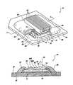
- the semiconductor device 10includes a semiconductor die 12 having an active surface 14 with bond pads 16 , as known in the art.
- the semiconductor die 12has a back side 18 which is bonded to a substrate 20 , shown here as a printed circuit board (PCB).
- the bond pads 16are shown as conventionally arrayed near the edges 32 of the semiconductor die 12 , and are wire-bonded with conductive, e.g., gold, wires 22 to corresponding electrical connection pads 24 on the substrate 20 . Leads on the upper surface 26 and below the upper surface 26 of the substrate 20 are not shown.
- a heat-conductive heat sink 30 with fins 28is mounted on the upper, i.e., active surface 14 of the semiconductor die 12 , between the rows of bond pads 16 .
- the heat sink 30has a relatively large exposed surface area, enabling a high transfer rate of thermal energy.
- An adhesive 34 having a high heat conductanceis preferably used, but other adhesives may be alternatively used to bond the heat sink 30 to the semiconductor die 12 , particularly because the adhesive 34 is applied in a very thin layer.
- a “glob top” material 38applied to encapsulate and seal the semiconductor die 12 , wires 22 , and surrounding portions 36 of the substrate 20 .
- a major portion of the heat sink 30is exposed to the ambient air for high heat transfer rates. If necessitated by very high heat generation, a fan (not shown) may be used in the appliance to further increase heat dissipation.
- the glob top material 38may be any suitable glob top material, an encapsulant type material, etc.
- the glob top material 38may be applied to overcover a major portion or all of the heat sink 30 . This results in decreased heat dissipation capability, however, but may be used where the thermal output of the semiconductor device permits.
- more than one semiconductor device 10may be attached to a single heat sink 30 , and together sealed by application of glob top material 38 .
- the heat sink 30is typically formed of a conductive metal such as aluminum, and has one attachment surface 46 which is attachable by adhesive 34 to the semiconductor die 12 .
- the heat sink 30may be of any design which provides the desired heat dissipation, is joinable to the die active surface 14 and sealable by a glob top material 38 .
- the heat sink 30may either have fins 28 or be finless.
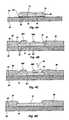
- FIGS. 3A through 3Gthe steps of fabricating semiconductor device 10 from a semiconductor die 12 , lead wires 22 and a heat sink 30 are outlined in more detail.
- a semiconductor die 12has an active surface 14 with bond pads 16 near opposing sides of the semiconductor die 12 .
- the back side 18 of the semiconductor die 12is first bonded to the upper surface 26 of the substrate 20 by a layer of adhesive 40 .
- the substrate 20may be a printed circuit board (PCB) or other materials such as a flex circuit or ceramic.
- a layer of a thermally conductive-filled gel elastomer 50may be either applied to the semiconductor die while in wafer form or subsequently applied to active surface 14 between the arrays of bond pads 16 of the semiconductor die 12 after singulation of the semiconductor die 12 from the wafer.
- the purpose of the gel elastomer 50is to provide a protective mask over an area of the semiconductor die 12 to which the heat sink 30 (FIG.
- the first layermay be retained on a portion of the semiconductor die 12 after the molding or glob-topping of the semiconductor die 12 for the attachment of a heat sink thereto, if desired (to be described in FIG. 3 C).
- the gel elastomer 50is applied as a gel or as a semi-solid or solid coupon.
- the gel elastomer 50or a suitable silicon elastomeric material, etc.
- the gel elastomer 50may include one or more dams 52 to help prevent the flow of any subsequently applied material from covering the surface of the gel elastomer 50 .
- the dams 52may extend along one or more sides of the semiconductor die 12 , as desired, and may be of any suitable height.
- the dams 52may be of any suitable material.
- the dams 52may comprise a second layer of gel elastomer 50 having a size smaller than that of the gel elastomer 50 .
- any glob top material 38 which lands on the gel elastomer 50will be later removed by removal of the gel elastomer from the active surface 14 of the semiconductor die 12 .
- the gel elastomer 50may be removed simply by peeling it from the active surface 14 of the semiconductor die 12 .
- a silicon type elastomermay be used on the semiconductor die 12 and removed therefrom for the application of a heat sink to the semiconductor die 12 .
- the gel elastomer 50is a recently developed material and includes Heat PathTM-filled cross-linked silicone gels sold by Raychem. As used in this invention, the gel elastomer 50 is filled with a conductive material to provide high thermal conductivity.
- the gel elastomer materialis compliant under light pressure, has a solid shape retention, cohesive strength and the ability to wet and adhere to surfaces.
- the bond pads 16are wire bonded to electrical connection pads 24 on the substrate 20 by e.g., thermosonic, thermocompression or ultrasonic methods, as known in the art.
- the wire bonding stepmay precede application of the gel elastomer 50 .
- FIG. 3Cdepicted is the next step of the process, that of applying glob top material 38 or suitable potting material to encapsulate the wire connections and the edges 32 (FIG. 3A) of the semiconductor die 12 .
- the glob top material 38is typically a thermally resistive polymer such as commercially available epoxy or urethane.
- the glob top material 38is typically applied as a curable liquid through a small nozzle, not shown, to extend to the layer of gel elastomer 50 , or nearly so.
- portions 38 A and 38 B of the glob top material 38have spilled onto the exposed surface 44 of gel elastomer 50 . Without use of the layer of gel elastomer 50 , effective removal of glob top portions 38 A and 38 B may damage the semiconductor die 12 and/or substrate 20 and/or lead wires 22 , etc.
- glob top material 38is followed by a curing step, such as by temperature elevation.
- the glob top material 38is cured to provide a hard, impenetrable sealing surface.
- the layer of gel elastomer 50is then peeled away in direction 42 from the active surface 14 of the semiconductor die 12 . It has been found that the lower surface 51 of the gel elastomer 50 may be easily and cleanly stripped from the active surface 14 of semiconductor die 12 by simply peeling away the gel elastomer coupon. This leaves the active surface 14 of the semiconductor die 12 clean and prepared for strong bonding of a heat sink 30 with an adhesive 34 , shown in drawing FIG. 3 E.
- die-to-substrate adhesives 40include those commonly known and/or used in the art. Examples of such are polyimides, a 75% silver-filled cyanate ester paste, an 80% silver-filled cyanate ester paste, a silver-filled lead glass paste, etc.
- the adhesive 34 used to bond the heat sink 30 to the active surface 14 of the semiconductor die 12may be an epoxy or the above identified die-to-substrate adhesives or an adhesive as known in the art.
- further glob top material 48may be applied to the semiconductor device 10 , particularly between the existing glob top material 38 and the heat sink 30 , for improved sealing.
- the glob top materials 38 and 48are shown overcovering the substrate 20 between semiconductor device 10 and an adjacent semiconductor device, of which only a connection pad 24 A and a bond wire 22 A are visible.
- the semiconductor device 10is effectively sealed to the substrate 20 to prevent electrical short-circuiting, wire breakage and debonding, and moisture penetration.
- a semiconductor die 12has an active surface 14 with bond pads 16 near opposing sides of the semiconductor die 12 .
- the back side 18 (FIG. 4A) of the semiconductor die 12is first bonded to the upper surface 26 of the substrate 20 by a layer of adhesive 40 .
- the substrate 20may be a printed circuit board (PCB) or other materials such as a flex circuit or ceramic.
- a layer of a thermally conductive-filled gel elastomer 50is either permanently applied to the semiconductor die while in wafer form or subsequently applied to active surface 14 between the arrays of bond pads 16 of the semiconductor die 12 after singulation of the semiconductor die 12 from the wafer.
- a layer or piece of disposable elastomer or tape 150is releasably applied over the gel elastomer 50 .
- the purpose of the elastomer or tape 150is to provide a protective mask over an area of the gel elastomer 50 attached to the semiconductor die 12 to which the heat sink 30 is to be bonded.
- the elastomer 150is applied as a semi-solid or solid coupon.
- the elastomer 150is to be disposed after removal from the semiconductor die 12 and may include one or more dams 52 to help prevent the flow of any subsequently applied material from covering the surface of the elastomer 150 .
- the dams 52may extend along one or more sides of the elastomer 150 , as desired, and may be of any suitable height.
- the dams 52may be of any suitable material.
- the dams 52may comprise a second layer of elastomer 150 having a size smaller than that of the gel elastomer 50 .
- Subsequent glob top applicationis difficult to precisely control, and any glob top material 38 which lands on the elastomer 150 will be later removed by removal of the elastomer 150 from the surface of the gel elastomer 50 .
- the elastomer 150may be removed simply by peeling it from the surface of the gel elastomer 50 permanently attached to the semiconductor die 12 .
- a silicon type elastomermay be used on the semiconductor die 12 and removed therefrom for the application of a heat sink to the semiconductor die 12 .
- the layer of elastomer 150is then peeled away in direction 42 from the surface of the gel elastomer 50 . It has been found that the lower surface 152 of the elastomer 150 may be easily and cleanly stripped from the surface of the gel elastomer 50 by simply peeling away the elastomer coupon. This leaves the surface of the gel elastomer 50 clean and prepared for strong bonding of a heat sink 30 with an adhesive 34 , shown in drawing FIG. 3 E.
- the glob top materials 38 and 48may be the same or different materials.
- Glob top materials useful for this applicationinclude HYSOLTM FP4451 material or HYSOLTM FP4450 high-purity, low-stress liquid encapsulant material, available from the DEXTER ELECTRONIC MATERIALS DIVISION OF DEXTER CORPORATION, etc.
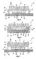
- FIG. 2Depicted in drawing FIG. 2 is another aspect of the invention, wherein the semiconductor die 12 is bonded flip-chip fashion to electrical circuit traces 54 on the upper surface 26 of substrate 20 .
- the semiconductor die 12has an active surface 14 with a grid of electrical connections 56 attached to the corresponding electrical circuit traces 54 .
- the electrical connections 56may comprise a ball grid array (BGA) of solder balls, as shown, or other array.
- BGAball grid array
- the opposite, back side 18 of the semiconductor die 12is directed upwardly, away from the substrate 20 .
- a heat sink 30here shown with fins 28 , has an attachment surface 46 which is adhesively bonded to the back side 18 with adhesive 34 .
- Glob top material 38is applied to seal the semiconductor die 12 , including its edges 32 , and a surrounding portion 36 of the substrate.
- a major portion of the heat sink 30is exposed to the ambient air for high heat transfer rates. Where very high heat dissipation rates are required, a fan (not shown) may be used to provide a high rate of air movement past the heat sink 30 .
- This type of attachmentmay similarly be used in chip scale packages, if desired. In such an instance, the semiconductor die 12 would be replaced by a chip scale package bonded flip-chip fashion to electrical circuit traces 54 on the upper surface 26 of substrate 20 .
- the chip scale packagehas an active surface 14 with a grid of electrical connections 56 attached to the corresponding electrical circuit traces 54 .
- the electrical connections 56may comprise a ball grid array (BGA) of solder balls, as shown, or other array.
- BGAball grid array
- a heat sink 30here shown with fins 28 , has an attachment surface 46 which is adhesively bonded to the back side 18 of the chip scale package with adhesive 34 .
- Glob top material 38is applied to seal the chip scale package, including its edges 32 , and a surrounding portion 36 of the substrate.
- a major portion of the heat sink 30is exposed to the ambient air for high heat transfer rates. Where very high heat dissipation rates are required, a fan (not shown) may be used to provide a high rate of air movement past the heat sink 30 .
- FIGS. 4A through 4FThe steps of fabricating the semiconductor device 10 of drawing FIG. 2 are illustrated in drawing FIGS. 4A through 4F. If a chip scale package is used rather than a semiconductor die 12 , all numerals and descriptions of the invention are the same except that the semiconductor die 12 is a chip scale package.
- the semiconductor die 12has an opposing back side 18 and edges 32 .
- the substrate 20may be a printed circuit board (PCB) or other material such as a flex circuit or ceramic.
- a layer or coupon of thermally conductive-filled gel elastomer 50alternatively, a suitable elastomer, silicon elastomeric material, etc.
- the gel elastomer 50is to be discarded, is applied as a solid or semisolid to the back side 18 of the semiconductor die 12 , either before or (preferably) after the semiconductor die 12 is electrically down bonded to the substrate 20 .
- the gel elastomer 50masks the back side 18 from glob top material 38 which may be inadvertently misapplied to the back side 18 , requiring removal by erosive blasting or other methods. The use of the gel elastomer 50 obviates such glob top removal methods.
- the next stepencompasses the application of glob top material 38 to encapsulate and seal the semiconductor die 12 and portions of the adjacent substrate upper surface 26 .
- the spaces 60 between the electrical connections 56are first filled with glob top material 38 or another low viscosity polymeric material.
- the glob top material 38is depicted as applied to form a nearly uniform depth over an extended substrate area. Some of the glob top material 38 is shown as having been misapplied to the layer of gel elastomer 50 as portions 38 A and 38 B.
- the glob top material 38is then cured, for example, by heating.
- the gel elastomer 50is then removed, e.g., by peeling it from the back side 18 of the semiconductor die 12 .
- the back side 18 of semiconductor die 12 in drawing FIG. 4Dis then bare and clean for enhanced attachment of a heat sink 30 thereto.
- a heat sink 30is bonded to the back side 18 of semiconductor die 12 by a layer of adhesive 34 , as already described relative to the embodiment of drawing FIG. 1 .
- a further application of a glob top material 48may be performed, particularly to fill the spaces between the glob top material 38 and the heat sink 30 .
- the glob top material 48may be the same as glob top material 38 , or may be different.
- RTVroom temperature vulcanizing rubber
- the heat sink 30may also be completely or nearly completely encapsulated.
- the Chip On Board semiconductor device 10 of drawing FIG. 1 or drawing FIG. 2may be formed as merely one of a plurality of components attached and sealed to a substrate.
- the chip scale package (CSP) semiconductor device 10may be a stand-alone encapsulated device whereby a grid of electrical connections is formed on the opposite side 58 (see FIG. 6) of the substrate 20 for bonding to another substrate, not shown.
- the gel elastomer 50may also be used as a permanent compliant member 70 between a semiconductor die 12 and a heat sink 30 .
- a semiconductor die 12has an active surface 14 with a ball grid array (BGA) of electrical connections 56 connected to traces (not shown) on a circuit board or other substrate 20 .
- a layer 70 of gel elastomeris then applied to inside attachment surface 46 of a cap style heat sink 30 .
- the heat sink 30may be finned, or have no fins 28 .
- the heat sink 30has lateral walls 62 whose lower edges 64 are designed to abut the upper surface 26 of the substrate 20 .
- a portion of the substrate 20is configured to fit within the open end 66 of the heat sink 30 .
- a semiconductor die 12has an active surface 14 with a ball grid array (BGA) of electrical connections 56 connected to traces (not shown) on a circuit board or other substrate 20 having a plurality of apertures 21 therein.
- BGAball grid array
- a layer 70 of gel elastomeris then applied to inside attachment surface 46 of a cap style heat sink 30 .
- the heat sink 30may be finned, or have no fins 28 .
- the heat sink 30has resilient spring members 31 having a portion thereof engaging a fin 28 while the other end thereof engages an aperture 21 of the substrate 20 to resiliently retain the heat sink 30 engaging the gel elastomer layer 70 which engages the back side 18 of the semiconductor die 12 , leaving the heat sink 30 and semiconductor die 12 free to move with respect to each other.
- the back side 18 of semiconductor die 12is then pressed into the gel elastomer layer 70 for attachment thereto.
- the adhesion of the gel elastomer layer 70 to the attachment surface 46 of the heat sink 30 and the back side 18 of the semiconductor die 12 as well as the resilient spring members 31holds the parts in place.
- the interior of the heat sink “cap”may be filled with encapsulant material 68 (as shown in FIG. 6 ).
- encapsulantmay be injected through holes (not shown) in the heat sink 30 .
- FIG. 6The embodiment of drawing FIG. 6 is shown with a further ball grid array (BGA) of solder balls 72 on the opposite side 58 of the substrate.
- BGAball grid array
- the semiconductor device 10may be bonded to another substrate, such as a circuit board, not shown.
- the elastomer layer 70is first applied to back side 18 of the semiconductor die 12 , which is then pressed into the attachment surface 46 of the heat sink 30 .
Landscapes
- Engineering & Computer Science (AREA)
- Microelectronics & Electronic Packaging (AREA)
- Physics & Mathematics (AREA)
- Condensed Matter Physics & Semiconductors (AREA)
- General Physics & Mathematics (AREA)
- Computer Hardware Design (AREA)
- Power Engineering (AREA)
- Manufacturing & Machinery (AREA)
- Cooling Or The Like Of Semiconductors Or Solid State Devices (AREA)
Abstract
Description
This application is a continuation of application Ser. No. 09/606,969, filed Jun. 28, 2000, now U.S. Pat. No. 6,432,840, issued Aug. 13, 2002, which is a continuation of application Ser. No. 09/146,945, filed Sep. 3, 1998, now U.S. Pat. No. 6,117,797, issued Sep. 12, 2000.
Field of the Invention: This invention relates generally to integrated circuit packages and methods of package assembly. More particularly, the present invention pertains to the manufacture of Chip On Board devices with heat sinks for high power dissipation.
State of the Art: Semiconductor devices are used in a wide variety of products, including computers, automobiles, integrated circuit cards, audio/video products, and a plethora of other electronic apparatus.
Modern electronic appliances such as computers have hundreds of integrated circuits (IC) and other electronic components, most of which are mounted on printed circuit boards (PCB). Heat is generated by such components. The heat generated by many ICs and other electronic components with simple circuits may often be dissipated without an additional heat sink. However, components requiring added heat sinks are becoming more numerous as the required speed, circuit complexity, and circuit density have increased.
In particular, as semiconductor devices have become more dense in terms of electrical power consumption per unit volume, heat generation has greatly increased, requiring package construction which dissipates the generated heat much more rapidly. As the state of the art progresses, the ability to adequately dissipate heat is often a severe constraint on the size, speed, and power consumption of an integrated circuit design.
The term “heat sink” is used herein in general reference to a passive heat transfer device, for example, an extruded aluminum plate with or without fins thereon. The plate is thermally coupled to an electronic component, e.g., semiconductor die, to absorb heat from the component and dissipate the heat by convection into the air. In this application, a heat sink will be distinguished from a “heat spreader,” the latter pertaining to a member which channels heat from a semiconductor die to leads which exit the die package. However, a heat sink and a heat spreader may together be used to cool a device.
Integrated circuit devices are constructed by making, e.g., a (silicon or germanium) semiconductor die with internal and surface circuits including transistors, resistors, capacitors, etc. A single semiconductor die may contain thousands of such components and generate considerable heat. Electrical connection pads on an “active” surface of the semiconductor die are connected to the various die circuits. The integrated circuit device also includes electrical leads enabling the electrical connection pads of the semiconductor die to be connected to circuits on a PCB (or other substrate) of an appliance.
Dissipation of generated thermal energy is necessary for safe operation of an electronic appliance. An excessively high temperature of an IC may cause a circuit board fire and damage or destroy the appliance. High temperatures cause failure of the integrated circuits themselves. State of the art methods for absorbing and dissipating thermal energy from high speed Chip On Board (COB) semiconductor devices are inadequate for any or all of the following reasons: (a) insufficient heat transfer capability, (b) excessively large package size, especially the profile height, (c) complexity of manufacture, and/or (d) excessive cost.
Current methods of forming glob topped Chip On Board devices with heat sinks are shown in U.S. Pat. No. 5,552,635 of Kim et al., U.S. Pat. No. 5,477,082 of Buckley III et al., U.S. Pat. No. 5,468,995 of Higgins III, U.S. Pat. No. 5,610,442 of Schneider et al., and U.S. Pat. No. 5,659,952 of Kovac et al.
In U.S. Pat. No. 5,450,283 of Lin et al., a method for making a semiconductor device with an exposed die back side is described. The method includes providing a printed wiring board (PWB) substrate with conductive traces, on which a semiconductor die is flip mounted and connected to the conductive traces. An electrically nonconductive coupling material is placed between the die and substrate. A package body is formed around the perimeter of the die, covering a portion of the conductive traces and any portion of the coupling material extending beyond the die perimeter. The back side of the die is left exposed through the use of a thin layer of tape placed in the mold cavity prior to the transfer molding of the package body around the die to prevent the flow of molding material forming the package from flowing on the inactive back side of the die. If the thin layer of tape adheres to the die after removal of the semiconductor device from the mold cavity, the thin layer of tape is removed from the die of the semiconductor device.
A device made with multiple layers of encapsulant is shown in U.S. Pat. No. 5,379,186 of Gold et al.
In accordance with the invention, an improved method for fabricating a Chip On Board semiconductor device requiring enhanced heat dissipation is applicable to direct attachment of semiconductor devices, such as dynamic memory semiconductor dice, to substrates, such as circuit boards and the like, and to the formation of modules incorporating a substrate, such as a circuit board.
In one aspect of the invention, an elastomer is used to cover a portion of a semiconductor die prior to glob top application of the die to the circuit board. The elastomer is removed, e.g., by peeling, from the die surface and includes any glob top material which has inadvertently been applied to the elastomer. Thus, the portion of the semiconductor die remains free of contaminants. If desired, since a portion of the semiconductor die is free of contaminants, providing a good adhesion surface, a heat sink may be attached to such portion of the semiconductor die. The method is applicable to both wire-bonded dies and flip-chip die bonding to circuit boards. Alternately, the elastomer may be retained on a portion of the semiconductor die after the molding or glob-topping of the die for the attachment of a heat sink thereto, if desired. The elastomer may be a highly thermally conductive elastomer to enhance the heat transfer from the semiconductor die to the surrounding environment. An example of a highly thermally conductive elastomer is a metal-filled elastomer or an elastomer filled with a highly thermally conductive material like metal.
The preferred elastomer is highly heat conductive, very compliant, has a relatively low adhesiveness and a high surface wetting property, all the type of properties that enhances heat transfer from the semiconductor die.
In another aspect of the invention, a heat conductive cap is formed over a semiconductor die and comprises a heat sink. A layer of the metal-filled gel elastomer is placed between the non-active surface of a die and the cap. Compressing the die into the cap forms the desired adhesion to retain the die within the cap. The compliance of the elastomer enables the die and cap to be pressed together without overpressuring the die/circuit board interface. In addition, the high thermal conductivity of the elastomer enables devices having a very high heat output to be cooled to temperatures enabling reliable operation.
The method of the invention includes steps for forming direct die-to-circuit board connections for “heat sinked” dice as well as for forming “heat sinked” die modules which may be themselves connected to a substrate such as a circuit board.
These and other features and advantages will be more clearly understood from the following detailed description when taken in conjunction with the accompanying drawings. It is important to note that the illustrations are not necessarily drawn to scale, and that there may be other embodiments of the invention which are not specifically illustrated. Like elements of the various figures are designated by like numerals.
The invention is illustrated in the following figures, wherein:
FIG. 1 is a perspective view of a wire-bonded Chip On Board (COB) semiconductor device of the invention;
FIG. 2 is a perspective view of a flip-chip Chip On Board (COB) semiconductor device of the invention;
FIGS. 3A through 3G are cross-sectional views of a wire-bonded Chip On Board (COB) semiconductor device illustrating the steps of fabrication in accordance with the invention, as taken alongline 3—3 of FIG. 1;
FIGS. 4A through 4F are cross-sectional views of a flip-chip Chip On Board (COB) semiconductor device illustrating the steps of fabrication in accordance with the invention, as taken along line4—4 of FIG. 2;
FIG. 5 is a cross-sectional view of a Chip On Board (COB) semiconductor device of the invention having a cap as a heat sink;
FIG. 6 is a cross-sectional view of a circuit board mounted semiconductor device of the invention having a cap as a heat sink; and
FIG. 7 is a cross-sectional view of a circuit board mounted semiconductor device of the invention having a heat sink resiliently retained on the semiconductor die.
As shown in drawing FIG. 1, afirst semiconductor device 10 with a high heat generation rate is shown. Thesemiconductor device 10 includes asemiconductor die 12 having anactive surface 14 withbond pads 16, as known in the art. The semiconductor die12 has aback side 18 which is bonded to asubstrate 20, shown here as a printed circuit board (PCB). Thebond pads 16 are shown as conventionally arrayed near theedges 32 of the semiconductor die12, and are wire-bonded with conductive, e.g., gold,wires 22 to correspondingelectrical connection pads 24 on thesubstrate 20. Leads on theupper surface 26 and below theupper surface 26 of thesubstrate 20 are not shown.
As shown, a heat-conductive heat sink 30 withfins 28 is mounted on the upper, i.e.,active surface 14 of the semiconductor die12, between the rows ofbond pads 16. Theheat sink 30 has a relatively large exposed surface area, enabling a high transfer rate of thermal energy. An adhesive34 having a high heat conductance is preferably used, but other adhesives may be alternatively used to bond theheat sink 30 to the semiconductor die12, particularly because the adhesive34 is applied in a very thin layer.
Also shown in drawing FIG. 1 is a “glob top”material 38 applied to encapsulate and seal the semiconductor die12,wires 22, and surroundingportions 36 of thesubstrate 20. A major portion of theheat sink 30 is exposed to the ambient air for high heat transfer rates. If necessitated by very high heat generation, a fan (not shown) may be used in the appliance to further increase heat dissipation. Theglob top material 38 may be any suitable glob top material, an encapsulant type material, etc.
In an alternative arrangement, theglob top material 38 may be applied to overcover a major portion or all of theheat sink 30. This results in decreased heat dissipation capability, however, but may be used where the thermal output of the semiconductor device permits.
It is evident that more than onesemiconductor device 10 may be attached to asingle heat sink 30, and together sealed by application ofglob top material 38.
Theheat sink 30 is typically formed of a conductive metal such as aluminum, and has oneattachment surface 46 which is attachable by adhesive34 to the semiconductor die12. Theheat sink 30 may be of any design which provides the desired heat dissipation, is joinable to the dieactive surface 14 and sealable by aglob top material 38. For example, theheat sink 30 may either havefins 28 or be finless.
Turning now to drawing FIGS. 3A through 3G, the steps of fabricatingsemiconductor device 10 from asemiconductor die 12,lead wires 22 and aheat sink 30 are outlined in more detail.
In drawing FIG. 3A, asemiconductor die 12 has anactive surface 14 withbond pads 16 near opposing sides of the semiconductor die12. Theback side 18 of the semiconductor die12 is first bonded to theupper surface 26 of thesubstrate 20 by a layer ofadhesive 40. Thesubstrate 20 may be a printed circuit board (PCB) or other materials such as a flex circuit or ceramic. A layer of a thermally conductive-filledgel elastomer 50 may be either applied to the semiconductor die while in wafer form or subsequently applied toactive surface 14 between the arrays ofbond pads 16 of the semiconductor die12 after singulation of the semiconductor die12 from the wafer. The purpose of thegel elastomer 50 is to provide a protective mask over an area of the semiconductor die12 to which the heat sink30 (FIG. 3E) is to be bonded. Alternatively, when a second layer is used as a mask, the first layer may be retained on a portion of the semiconductor die12 after the molding or glob-topping of the semiconductor die12 for the attachment of a heat sink thereto, if desired (to be described in FIG.3C). Thegel elastomer 50 is applied as a gel or as a semi-solid or solid coupon. Thegel elastomer 50, or a suitable silicon elastomeric material, etc. if thegel elastomer 50 is to be disposed after removal from the semiconductor die12, or the use of a metal-filledgel elastomer 50, if such is to remain on the semiconductor die12, may include one ormore dams 52 to help prevent the flow of any subsequently applied material from covering the surface of thegel elastomer 50. Thedams 52 may extend along one or more sides of the semiconductor die12, as desired, and may be of any suitable height. Thedams 52 may be of any suitable material. Alternately, thedams 52 may comprise a second layer ofgel elastomer 50 having a size smaller than that of thegel elastomer 50. Subsequent glob top application is difficult to precisely control, and anyglob top material 38 which lands on thegel elastomer 50 will be later removed by removal of the gel elastomer from theactive surface 14 of the semiconductor die12. Typically, thegel elastomer 50 may be removed simply by peeling it from theactive surface 14 of the semiconductor die12. Typically, if thegel elastomer 50 is to be removed from the semiconductor die12 after the glob top material application, a silicon type elastomer may be used on the semiconductor die12 and removed therefrom for the application of a heat sink to the semiconductor die12.
Thegel elastomer 50 is a recently developed material and includes Heat Path™-filled cross-linked silicone gels sold by Raychem. As used in this invention, thegel elastomer 50 is filled with a conductive material to provide high thermal conductivity. The gel elastomer material is compliant under light pressure, has a solid shape retention, cohesive strength and the ability to wet and adhere to surfaces.
In the next step, shown in drawing FIG. 3B, thebond pads 16 are wire bonded toelectrical connection pads 24 on thesubstrate 20 by e.g., thermosonic, thermocompression or ultrasonic methods, as known in the art.
Alternatively, the wire bonding step may precede application of thegel elastomer 50.
In drawing FIG. 3C, depicted is the next step of the process, that of applyingglob top material 38 or suitable potting material to encapsulate the wire connections and the edges32 (FIG. 3A) of the semiconductor die12. Theglob top material 38 is typically a thermally resistive polymer such as commercially available epoxy or urethane. Theglob top material 38 is typically applied as a curable liquid through a small nozzle, not shown, to extend to the layer ofgel elastomer 50, or nearly so. As shown,portions glob top material 38 have spilled onto the exposedsurface 44 ofgel elastomer 50. Without use of the layer ofgel elastomer 50, effective removal of globtop portions substrate 20 and/or leadwires 22, etc.
Application of theglob top material 38 is followed by a curing step, such as by temperature elevation. Theglob top material 38 is cured to provide a hard, impenetrable sealing surface.
As shown in drawing FIG. 3D, the layer ofgel elastomer 50 is then peeled away indirection 42 from theactive surface 14 of the semiconductor die12. It has been found that thelower surface 51 of thegel elastomer 50 may be easily and cleanly stripped from theactive surface 14 of semiconductor die12 by simply peeling away the gel elastomer coupon. This leaves theactive surface 14 of the semiconductor die12 clean and prepared for strong bonding of aheat sink 30 with an adhesive34, shown in drawing FIG.3E.
The particular materials which may be used as die-to-substrate adhesives 40 include those commonly known and/or used in the art. Examples of such are polyimides, a 75% silver-filled cyanate ester paste, an 80% silver-filled cyanate ester paste, a silver-filled lead glass paste, etc.
The adhesive34 used to bond theheat sink 30 to theactive surface 14 of the semiconductor die12 may be an epoxy or the above identified die-to-substrate adhesives or an adhesive as known in the art.
As illustrated in drawing FIG. 3F, further globtop material 48 may be applied to thesemiconductor device 10, particularly between the existingglob top material 38 and theheat sink 30, for improved sealing. In this figure, theglob top materials substrate 20 betweensemiconductor device 10 and an adjacent semiconductor device, of which only aconnection pad 24A and abond wire 22A are visible. Thesemiconductor device 10 is effectively sealed to thesubstrate 20 to prevent electrical short-circuiting, wire breakage and debonding, and moisture penetration.
In drawing FIG. 3G, asemiconductor die 12 has anactive surface 14 withbond pads 16 near opposing sides of the semiconductor die12. The back side18 (FIG. 4A) of the semiconductor die12 is first bonded to theupper surface 26 of thesubstrate 20 by a layer ofadhesive 40. Thesubstrate 20 may be a printed circuit board (PCB) or other materials such as a flex circuit or ceramic. A layer of a thermally conductive-filledgel elastomer 50 is either permanently applied to the semiconductor die while in wafer form or subsequently applied toactive surface 14 between the arrays ofbond pads 16 of the semiconductor die12 after singulation of the semiconductor die12 from the wafer. A layer or piece of disposable elastomer ortape 150 is releasably applied over thegel elastomer 50. The purpose of the elastomer ortape 150 is to provide a protective mask over an area of thegel elastomer 50 attached to the semiconductor die12 to which theheat sink 30 is to be bonded. Theelastomer 150 is applied as a semi-solid or solid coupon. Theelastomer 150 is to be disposed after removal from the semiconductor die12 and may include one ormore dams 52 to help prevent the flow of any subsequently applied material from covering the surface of theelastomer 150. Thedams 52 may extend along one or more sides of theelastomer 150, as desired, and may be of any suitable height. Thedams 52 may be of any suitable material. Alternately, thedams 52 may comprise a second layer ofelastomer 150 having a size smaller than that of thegel elastomer 50. Subsequent glob top application is difficult to precisely control, and anyglob top material 38 which lands on theelastomer 150 will be later removed by removal of theelastomer 150 from the surface of thegel elastomer 50. Typically, theelastomer 150 may be removed simply by peeling it from the surface of thegel elastomer 50 permanently attached to the semiconductor die12. Typically, if theelastomer 150 is to be removed from thegel elastomer 50 after the glob top material application, a silicon type elastomer may be used on the semiconductor die12 and removed therefrom for the application of a heat sink to the semiconductor die12.
As shown in drawing FIG. 3G, the layer ofelastomer 150 is then peeled away indirection 42 from the surface of thegel elastomer 50. It has been found that thelower surface 152 of theelastomer 150 may be easily and cleanly stripped from the surface of thegel elastomer 50 by simply peeling away the elastomer coupon. This leaves the surface of thegel elastomer 50 clean and prepared for strong bonding of aheat sink 30 with an adhesive34, shown in drawing FIG.3E.
Theglob top materials
Depicted in drawing FIG. 2 is another aspect of the invention, wherein the semiconductor die12 is bonded flip-chip fashion to electrical circuit traces54 on theupper surface 26 ofsubstrate 20. The semiconductor die12 has anactive surface 14 with a grid ofelectrical connections 56 attached to the corresponding electrical circuit traces54. Theelectrical connections 56 may comprise a ball grid array (BGA) of solder balls, as shown, or other array. The opposite, backside 18 of the semiconductor die12 is directed upwardly, away from thesubstrate 20. Aheat sink 30, here shown withfins 28, has anattachment surface 46 which is adhesively bonded to theback side 18 withadhesive 34. Globtop material 38 is applied to seal the semiconductor die12, including itsedges 32, and a surroundingportion 36 of the substrate. A major portion of theheat sink 30 is exposed to the ambient air for high heat transfer rates. Where very high heat dissipation rates are required, a fan (not shown) may be used to provide a high rate of air movement past theheat sink 30. This type of attachment may similarly be used in chip scale packages, if desired. In such an instance, the semiconductor die12 would be replaced by a chip scale package bonded flip-chip fashion to electrical circuit traces54 on theupper surface 26 ofsubstrate 20. The chip scale package has anactive surface 14 with a grid ofelectrical connections 56 attached to the corresponding electrical circuit traces54. Theelectrical connections 56 may comprise a ball grid array (BGA) of solder balls, as shown, or other array. The opposite, backside 18 of the chip scale package is directed upwardly, away from thesubstrate 20. Aheat sink 30, here shown withfins 28, has anattachment surface 46 which is adhesively bonded to theback side 18 of the chip scale package with adhesive34. Globtop material 38 is applied to seal the chip scale package, including itsedges 32, and a surroundingportion 36 of the substrate. A major portion of theheat sink 30 is exposed to the ambient air for high heat transfer rates. Where very high heat dissipation rates are required, a fan (not shown) may be used to provide a high rate of air movement past theheat sink 30.
The steps of fabricating thesemiconductor device 10 of drawing FIG. 2 are illustrated in drawing FIGS. 4A through 4F. If a chip scale package is used rather than asemiconductor die 12, all numerals and descriptions of the invention are the same except that the semiconductor die12 is a chip scale package.
As depicted in drawing FIG. 4A, a flip-chip or semiconductor die12 having anactive surface 14 with a grid ofelectrical connections 56, shown as solder balls, is down bonded to electrical circuit traces54 (not shown) on anupper surface 26 of asubstrate 20. The semiconductor die12 has an opposing backside 18 and edges32. Thesubstrate 20 may be a printed circuit board (PCB) or other material such as a flex circuit or ceramic. A layer or coupon of thermally conductive-filledgel elastomer 50, alternatively, a suitable elastomer, silicon elastomeric material, etc. if thegel elastomer 50 is to be discarded, is applied as a solid or semisolid to theback side 18 of the semiconductor die12, either before or (preferably) after the semiconductor die12 is electrically down bonded to thesubstrate 20. Thegel elastomer 50 masks theback side 18 from globtop material 38 which may be inadvertently misapplied to theback side 18, requiring removal by erosive blasting or other methods. The use of thegel elastomer 50 obviates such glob top removal methods.
As shown in drawing FIG. 4B, the next step encompasses the application ofglob top material 38 to encapsulate and seal the semiconductor die12 and portions of the adjacent substrateupper surface 26. Preferably, thespaces 60 between theelectrical connections 56 are first filled withglob top material 38 or another low viscosity polymeric material. In these figures, theglob top material 38 is depicted as applied to form a nearly uniform depth over an extended substrate area. Some of theglob top material 38 is shown as having been misapplied to the layer ofgel elastomer 50 asportions
Theglob top material 38 is then cured, for example, by heating.
As shown in drawing FIG. 4C, thegel elastomer 50 is then removed, e.g., by peeling it from theback side 18 of the semiconductor die12. Theback side 18 of semiconductor die12 in drawing FIG. 4D is then bare and clean for enhanced attachment of aheat sink 30 thereto.
In drawing FIG. 4E, aheat sink 30 is bonded to theback side 18 of semiconductor die12 by a layer of adhesive34, as already described relative to the embodiment of drawing FIG.1.
In drawing FIG. 4F, a further application of aglob top material 48 may be performed, particularly to fill the spaces between the globtop material 38 and theheat sink 30. Theglob top material 48 may be the same as globtop material 38, or may be different.
Alternatively, a room temperature vulcanizing rubber (RTV), which may vary in the degree of thermal conductivity thereof, may be used to completely cover and seal the semiconductor device to thesubstrate 20, including theglob top material 38.
Although a major portion of theheat sink 30 is unencapsulated in the preferred embodiment, the heat sink may also be completely or nearly completely encapsulated.
The Chip OnBoard semiconductor device 10 of drawing FIG. 1 or drawing FIG. 2 may be formed as merely one of a plurality of components attached and sealed to a substrate. Alternatively, the chip scale package (CSP)semiconductor device 10 may be a stand-alone encapsulated device whereby a grid of electrical connections is formed on the opposite side58 (see FIG. 6) of thesubstrate 20 for bonding to another substrate, not shown.
While application of thegel elastomer 50 to the semiconductor die12, when singulated or while in wafer form, is an additional step in device fabrication, it eliminates the troublesome step of glob top removal required by misapplication of glob top material to the die surface. A clean surface for bonding to a heat sink is assured. In addition, no other layers of good conductors and/or poor conductors are required, enabling both (a) high heat removal and (b) a device of reduced dimensions.
Thegel elastomer 50 may also be used as a permanentcompliant member 70 between asemiconductor die 12 and aheat sink 30. As depicted in drawing FIG. 5, asemiconductor die 12 has anactive surface 14 with a ball grid array (BGA) ofelectrical connections 56 connected to traces (not shown) on a circuit board orother substrate 20. Alayer 70 of gel elastomer is then applied toinside attachment surface 46 of a capstyle heat sink 30. Theheat sink 30 may be finned, or have nofins 28. In one embodiment, theheat sink 30 haslateral walls 62 whoselower edges 64 are designed to abut theupper surface 26 of thesubstrate 20. Alternatively (FIG.6), a portion of thesubstrate 20 is configured to fit within theopen end 66 of theheat sink 30.
As depicted in drawing FIG. 7, asemiconductor die 12 has anactive surface 14 with a ball grid array (BGA) ofelectrical connections 56 connected to traces (not shown) on a circuit board orother substrate 20 having a plurality ofapertures 21 therein. Alayer 70 of gel elastomer is then applied toinside attachment surface 46 of a capstyle heat sink 30. Theheat sink 30 may be finned, or have nofins 28. In one embodiment, theheat sink 30 hasresilient spring members 31 having a portion thereof engaging afin 28 while the other end thereof engages anaperture 21 of thesubstrate 20 to resiliently retain theheat sink 30 engaging thegel elastomer layer 70 which engages theback side 18 of the semiconductor die12, leaving theheat sink 30 and semiconductor die12 free to move with respect to each other.
In either case, as illustrated in drawing FIGS. 5,6, and7, theback side 18 of semiconductor die12 is then pressed into thegel elastomer layer 70 for attachment thereto. The adhesion of thegel elastomer layer 70 to theattachment surface 46 of theheat sink 30 and theback side 18 of the semiconductor die12 as well as theresilient spring members 31 holds the parts in place.
As a further step, the interior of the heat sink “cap” may be filled with encapsulant material68 (as shown in FIG.6). In the embodiment of drawing FIG. 5, encapsulant may be injected through holes (not shown) in theheat sink 30.
The embodiment of drawing FIG. 6 is shown with a further ball grid array (BGA) ofsolder balls 72 on theopposite side 58 of the substrate. Thus, thesemiconductor device 10 may be bonded to another substrate, such as a circuit board, not shown.
In an alternate method of forming the semiconductor devices of drawing FIGS. 5 and 6, theelastomer layer 70 is first applied to backside 18 of the semiconductor die12, which is then pressed into theattachment surface 46 of theheat sink 30.
In the embodiments of drawing FIGS. 5 and 6, overpressuring of the die/substrate interface is eliminated by the compliance of the filled gel elastomer. Simultaneously, the high thermal conductivity of the filled gel elastomer maintains high heat dissipation from the device.
It is apparent to those skilled in the art that various changes and modifications may be to the method and apparatus of the invention as disclosed herein without departing from the spirit and scope of the invention as defined in the following claims.
Claims (90)
1. A method for preventing material from adhering to at least a portion of a surface of a semiconductor die, comprising:
applying a layer of material for masking a portion of said surface of said semiconductor die, said
layer including at least one of a gel, an elastomeric material, and a material having filler particles therein;
applying an encapsulant material to a remaining portion of said surface of said semiconductor die;
curing said encapsulant material; and
removing at least a portion of said layer of material from at least a portion of said surface of said semiconductor die.
2. The method ofclaim 1 , wherein said layer of material includes a silicon gel material.
3. The method ofclaim 1 , wherein said layer of material includes a silicon elastomeric material.
4. The method ofclaim 1 , wherein said layer of material includes a material selected from the group consisting of natural rubber, synthetic rubber, and room temperature-cured silicon rubber.
5. The method ofclaim 2 , wherein said silicon gel material includes a cross-linked silicon gel material.
6. The method ofclaim 5 , wherein said silicon gel material includes a cross-linked silicon gel material having at least one thermally conductive filler material therein.
7. The method ofclaim 6 , wherein said silicon gel material includes a cross-linked silicon gel material having a plurality of thermally conductive filler materials therein.
8. The method ofclaim 1 , wherein said semiconductor die is bonded to a substrate in a Chip On Board configuration.
9. The method ofclaim 1 , further comprising:
providing a heat sink having at least one surface; and
securing said heat sink to said surface of said semiconductor die.
10. The method ofclaim 2 , wherein said silicon gel material includes a gel elastomer material filled with heat conductive particles whereby heat conductivity is enhanced.
11. The method ofclaim 10 , wherein said heat conductive particles include metal particles, carbon particles, and diamond-filled thermally conductive material in particle form.
12. The method ofclaim 1 , wherein said layer of material includes a dam extending a portion of a length of at least one side of said semiconductor die.
13. The method ofclaim 12 , wherein said dam extends a portion of a length of a plurality of sides of said semiconductor die.
14. The method ofclaim 9 , wherein said heat sink is resiliently mounted to said surface of said semiconductor die.
15. A method for preventing at least a portion of a material from adhering to at least a portion of a surface of a chip scale semiconductor package, comprising:
applying a layer of material as a mask to at least a portion of said surface of said chip scale semiconductor package, said layer including at least one of a gels a material having a filler therein and an elastomeric material;
applying an encapsulant material to a remaining portion of said surface of said chip scale semiconductor package;
curing said encapsulant material; and
removing at least a portion of said layer of material from at least a portion of said surface of said chip scale semiconductor package.
16. The method ofclaim 15 , wherein said layer of material includes a silicon gel material.
17. The method ofclaim 15 , wherein said layer of material includes a silicon elastomeric material.
18. The method ofclaim 15 , wherein said layer of material includes a material selected from the group consisting of natural rubber, synthetic rubber, and room temperature-cured silicon rubber.
19. The method ofclaim 16 , wherein said silicon gel material includes a cross-linked silicon gel material.
20. The method ofclaim 19 , wherein said silicon gel material includes a cross-linked silicon gel material having at least one thermally conductive filler material therein.
21. The method ofclaim 20 , wherein said silicon gel material includes a cross-linked silicon gel material having a plurality of thermally conductive filler materials therein.
22. The method ofclaim 15 , wherein said chip scale semiconductor package is bonded to a substrate in a Chip On Board configuration.
23. The method ofclaim 22 , further comprising:
providing a heat sink having at least one surface; and
securing said heat sink to said surface of said chip scale semiconductor package.
24. The method ofclaim 16 , wherein said silicon gel material includes a gel elastomer material filled with heat conductive particles whereby heat conductivity is enhanced.
25. The method ofclaim 24 , wherein said heat conductive particles include metal particles, carbon particles, and diamond-filled thermally conductive material in particle form.
26. The method ofclaim 15 , wherein said layer of material includes a dam extending a portion of a length of at least one side of said chip scale semiconductor package.
27. The method ofclaim 26 , wherein said dam extends a portion of a length of a plurality of sides of said chip scale semiconductor package.
28. A method for preventing at least a portion of glob top material from adhering to at least a portion of a surface of a semiconductor die, comprising:
applying a first layer of material to said surface of said semiconductor die, said first layer of material including at least one of a gel, a material having a filler therein, and an elastomeric material;
applying a second layer of material as a mask to a portion of a surface of said first layer of material;
applying an encapsulant material to a remaining portion of said surface of said semiconductor die;
curing said encapsulant material; and
removing at least a portion of said first layer of material from at least a portion of said surface of said semiconductor die.
29. The method ofclaim 28 , wherein said first layer of material and said second layer of material include a silicon gel material.
30. The method ofclaim 28 , wherein said first layer of material and said second layer of material include a silicon elastomeric material.
31. The method ofclaim 28 , wherein said second layer of material includes a material selected from the group consisting of natural rubber, synthetic rubber, and room temperature-cured silicon rubber.
32. The method ofclaim 29 , wherein said silicon gel material includes a cross-linked silicon gel material.
33. The method ofclaim 32 , wherein said silicon gel material includes a cross-linked silicon gel material having at least one thermally conductive filler material therein.
34. The method ofclaim 33 , wherein said silicon gel material includes a cross-linked silicon gel material having a plurality of thermally conductive filler materials therein.
35. The method ofclaim 28 , wherein said semiconductor die is bonded to a substrate in a Chip On Board configuration.
36. The method ofclaim 28 , further comprising:
providing a heat sink having at least one surface; and
securing said heat sink to a surface of said second layer of material.
37. The method ofclaim 29 , wherein said silicon gel material includes a gel elastomer material filled with heat conductive particles whereby heat conductivity is enhanced.
38. The method ofclaim 37 , wherein said heat conductive particles include metal particles, carbon particles, and diamond-filled thermally conductive material in particle form.
39. The method ofclaim 28 , wherein said second layer of material includes a dam extending a portion of a length of at least one side of said semiconductor die.
40. The method ofclaim 39 , wherein said dam extends a portion of a length of a plurality of sides of said semiconductor die.
41. A method for preventing at least a portion of glob top material from adhering to at least a portion of a surface of a semiconductor die, comprising:
applying a layer of material as a mask to a portion of said surface of said semiconductor die said layer including at least one of a gel, a material having a filler therein, and an elastomeric material;
applying glob top material to a remaining portion of said surface of said semiconductor die;
curing said glob top material; and
removing at least a portion of said layer of material from at least a portion of said surface of said semiconductor die.
42. The method ofclaim 41 , wherein said layer of material includes a silicon gel material.
43. The method ofclaim 41 , wherein said layer of material includes an elastomeric material.
44. The method ofclaim 41 , wherein said layer of material includes a material selected from the group consisting of natural rubber, synthetic rubber, and room temperature-cured silicon rubber.
45. The method ofclaim 42 , wherein said silicon gel material includes a cross-linked silicon gel material.
46. The method ofclaim 45 , wherein said silicon gel material includes a cross-linked silicon gel material having at least one thermally conductive filler material therein.
47. The method ofclaim 46 , wherein said silicon gel material includes a cross-linked silicon gel material having a plurality of thermally conductive filler materials therein.
48. The method ofclaim 41 , wherein said semiconductor die is bonded to a substrate in a Chip On Board configuration.
49. The method ofclaim 41 , further comprising:
providing a heat sink having at least one surface; and
securing said heat sink to said surface of said semiconductor die.
50. The method ofclaim 42 , wherein said silicon gel material includes a gel elastomer material filled with heat conductive particles whereby heat conductivity is enhanced.
51. The method ofclaim 50 , wherein said heat conductive particles include metal particles.
52. The method ofclaim 41 , wherein said layer of material includes a dam extending a portion of a length of one side of said semiconductor die.
53. The method ofclaim 52 , wherein said dam extends a portion of a length of a plurality of sides of said semiconductor die.
54. A method for fabricating a Chip On Board semiconductor device with a heat sink, said method comprising:
providing a semiconductor die having a first side, a second side, and edges therebetween;
providing a substrate;
providing a thermally conductive heat sink member;
attaching at least a portion of said first side of said semiconductor die to a portion of said substrate;
covering at least a portion of said second side of said semiconductor die with a material having an exposed surface, said material including at least one of a gel, a material having a filler therein and an elastomeric material;
applying a material to encapsulate said edges of said semiconductor die;
maintaining said exposed surface of said material covering said at least a portion of said second side of said semiconductor die substantially unencapsulated;
curing said material to encapsulate said edges of said semiconductor die;
removing said material having an exposed surface covering said at least a portion of said second side of said semiconductor die; and
attaching a portion of said heat sink member to at least a portion of said second side of said semiconductor die.
55. The method ofclaim 54 , wherein providing a semiconductor die includes providing a semiconductor die having wire bond pads; and wirebonding said wire bond pads of said semiconductor die to said substrate.
56. The method ofclaim 55 , wherein said heat sink member is attached to said semiconductor die between said wire bond pads of said semiconductor die.
57. The method ofclaim 54 , wherein providing a semiconductor die includes providing a semiconductor die having a surface having a grid of circuit connections configured for downbonding to said substrate; and attaching said semiconductor die to said substrate includes attaching said grid of circuit connections to said substrate.
58. The method ofclaim 57 , wherein said heat sink member is attached to at least a portion of a non-active back side surface of said semiconductor die.
59. The method ofclaim 54 , wherein said substrate is a printed circuit board.
60. The method ofclaim 54 , wherein covering said at least a portion of said second side of said semiconductor die comprises covering said at least a portion of said second side of said semiconductor die with a thermally conductive gel elastomer filled with thermally conductive particles.
61. The method ofclaim 60 , wherein said thermally conductive gel elastomer comprises cross-linked silicone.
62. The method ofclaim 60 , wherein said thermally conductive gel elastomer is filled with metal particles.
63. The method ofclaim 54 , wherein attaching said heat sink includes attaching said heat sink member to said second side of said semiconductor die with a thermally conductive adhesive.
64. The method ofclaim 54 , wherein attaching said heat sink includes attaching said heat sink member to said second side of said semiconductor die with a polymeric tape.
65. A method for preventing at least a portion of a glob top material from adhering to at least a portion of a surface of a semiconductor die, comprising:
applying a layer of at least one of a material having filler therein and a gel elastomer material as a mask to a portion of said surface of said semiconductor die;
applying glob top material to the remaining portion of said surface of said semiconductor die;
curing said glob top material; and
peeling at least a portion of said gel elastomer material from at least a portion of said surface of said semiconductor die.
66. The method ofclaim 65 , wherein said semiconductor die is attached to a substrate in a Chip On Board configuration.
67. The method ofclaim 65 , further comprising:
attaching a surface of a heat sink to said surface of said semiconductor die.
68. The method ofclaim 67 , wherein said gel elastomer material includes a gel elastomer material filled with particles.
69. A method for fabricating a Chip On Board semiconductor device having a heat sink, said method comprising:
providing a semiconductor die having a first side, a second side, edges therebetween, and electrical terminals;
providing a substrate having electrical connections;
providing a thermally conductive heat sink member; attaching at least a portion of said first side of said semiconductor die to at least a portion of said substrate;
connecting at least one electrical terminal of said electrical terminals of said semiconductor die to at least one electrical connection of said electrical connections of said substrate;
covering at least a portion of said second side of said semiconductor die with a compliant protective layer having an exposed surface, said layer comprising at least one of a material having a filler therein and an elastomer;
applying a material to encapsulate said at least one electrical terminal of said electrical terminals and at least one edge of said edges of said semiconductor die;
maintaining at least a portion of said exposed surface of said protective layer substantially unencapsulated by said material; curing said material;
removing at least a portion of said protective layer; and attaching a portion of said heat sink member to a portion of said second side of said semiconductor die.
70. The method ofclaim 69 , wherein providing a semiconductor die includes providing a semiconductor die having wire bond pads: and
connecting said electrical terminals of said semiconductor die includes wirebonding said electrical terminals of said semiconductor die to said electrical connections of said substrate.
71. The method ofclaim 70 , wherein said heat sink member is attached to said second side of said semiconductor die between said electrical terminals of said semiconductor die.
72. The method ofclaim 69 , wherein providing a semiconductor die includes providing a semiconductor die having an active surface with a grid of circuit connections configured for bonding to said substrate; and
connecting said electrical terminals of said semiconductor die to said electrical connections of said substrate includes bonding said grid of circuit connections to said electrical connections on said substrate.
73. The method ofclaim 72 , wherein said heat sink member is attached to a non-active back side surface of said semiconductor die.
74. The method ofclaim 69 , wherein said substrate is a printed circuit board.
75. The method ofclaim 69 , wherein covering said at least a portion of said second side of said semiconductor die includes covering said at least a portion of said second side of said semiconductor die with a thermally conductive gel elastomer filled with thermally conductive particles.
76. The method ofclaim 75 , wherein said gel elastomer filled with thermally conductive particles comprises cross-linked silicone.
77. The method ofclaim 75 , wherein said gel elastomer filled with thermally conductive particles includes a gel elastomer filled with metal particles.
78. The method ofclaim 77 , wherein attaching said heat sink member includes attaching said heat sink member to said second side of said semiconductor die with a non-stress thermally conductive adhesive.
79. The method ofclaim 78 , wherein attaching said heat sink member includes attaching said heat sink member to said second side of said semiconductor die with a polymeric tape.
80. A fabrication method for a semiconductor device assembly having a heat sink, said method comprising:
providing a semiconductor die having a first side, a second side, and edges therebetween;
providing a substrate;
providing a thermally conductive heat sink member;
attaching at least a portion of said first side of said semiconductor die to at least a portion of said substrate;
covering at least a portion of said second side of said semiconductor die with a material having an exposed surface, said material comprising at least one of a material having a filler therein and an elastomeric material;
applying a material to encapsulate at least a portion of one edge of said edges of said semiconductor die;
maintaining said exposed surface of said material covering said at least a portion of said second side of said semiconductor die substantially unencapsulated;
curing said material to encapsulate said at least a portion of one edge of said edges of said semiconductor die;
removing at least a portion of said material having an exposed surface covering said at least a portion of said second side of said semiconductor die; and
attaching at least a portion of said heat sink member to a portion of said second side of said semiconductor die.
81. The method ofclaim 80 , wherein providing a semiconductor die includes providing a semiconductor die having wire bond pads; and
wirebonding said wire bond pads of said semiconductor die to said substrate.
82. The method ofclaim 81 , wherein said heat sink member is attached to said semiconductor die between said wire bond pads of said semiconductor die.
83. The method ofclaim 80 , wherein providing a semiconductor die includes providing a semiconductor die having a surface having a grid of circuit connections configured for downbonding to said substrate; and
attaching said semiconductor die to said substrate includes attaching said grid of circuit connections to said substrate.
84. The method ofclaim 83 , wherein said heat sink member is attached to a non-active back side surface of said semiconductor die.
85. The method ofclaim 80 , wherein said substrate is a printed circuit board.
86. The method ofclaim 80 , wherein covering said at least a portion of said second side of said semiconductor die comprises covering said at least a portion of said second side of said semiconductor die with a thermally conductive gel elastomer filled with thermally conductive particles.
87. The method ofclaim 86 , wherein said thermally conductive gel elastomer comprises cross-linked silicone.
88. The method ofclaim 86 , wherein said thermally conductive gel elastomer is filled with metal particles.
89. The method ofclaim 80 , wherein attaching said heat sink includes attaching said heat sink member to said second side of said semiconductor die with a thermally conductive adhesive.
90. The method ofclaim 80 , wherein attaching said heat sink includes attaching said heat sink member to said second side of said semiconductor die with a polymeric tape.
Priority Applications (1)
| Application Number | Priority Date | Filing Date | Title |
|---|---|---|---|
| US10/200,929US6784113B2 (en) | 1998-09-03 | 2002-07-22 | Chip on board and heat sink attachment methods |
Applications Claiming Priority (3)
| Application Number | Priority Date | Filing Date | Title |
|---|---|---|---|
| US09/146,945US6117797A (en) | 1998-09-03 | 1998-09-03 | Attachment method for heat sinks and devices involving removal of misplaced encapsulant |
| US09/606,969US6432840B1 (en) | 1998-09-03 | 2000-06-28 | Methodology of removing misplaced encapsulant for attachment of heat sinks in a chip on board package |
| US10/200,929US6784113B2 (en) | 1998-09-03 | 2002-07-22 | Chip on board and heat sink attachment methods |
Related Parent Applications (1)
| Application Number | Title | Priority Date | Filing Date |
|---|---|---|---|
| US09/606,969ContinuationUS6432840B1 (en) | 1998-09-03 | 2000-06-28 | Methodology of removing misplaced encapsulant for attachment of heat sinks in a chip on board package |
Publications (2)
| Publication Number | Publication Date |
|---|---|
| US20020182781A1 US20020182781A1 (en) | 2002-12-05 |
| US6784113B2true US6784113B2 (en) | 2004-08-31 |
Family
ID=22519689
Family Applications (10)
| Application Number | Title | Priority Date | Filing Date |
|---|---|---|---|
| US09/146,945Expired - LifetimeUS6117797A (en) | 1998-09-03 | 1998-09-03 | Attachment method for heat sinks and devices involving removal of misplaced encapsulant |
| US09/511,609Expired - LifetimeUS6596565B1 (en) | 1998-09-03 | 2000-02-23 | Chip on board and heat sink attachment methods |
| US09/510,890Expired - LifetimeUS6451709B1 (en) | 1998-09-03 | 2000-02-23 | Methodology of removing misplaced encapsulant for attachment of heat sinks in a chip on board package |
| US09/510,894Expired - LifetimeUS6229204B1 (en) | 1998-09-03 | 2000-02-23 | Chip on board with heat sink attachment |
| US09/606,969Expired - LifetimeUS6432840B1 (en) | 1998-09-03 | 2000-06-28 | Methodology of removing misplaced encapsulant for attachment of heat sinks in a chip on board package |
| US09/834,297Expired - Fee RelatedUS6806567B2 (en) | 1998-09-03 | 2001-04-12 | Chip on board with heat sink attachment and assembly |
| US10/189,097Expired - LifetimeUS6630371B2 (en) | 1998-09-03 | 2002-07-02 | Chip on board and heat sink attachment methods |
| US10/200,929Expired - Fee RelatedUS6784113B2 (en) | 1998-09-03 | 2002-07-22 | Chip on board and heat sink attachment methods |
| US10/624,332Expired - Fee RelatedUS7244637B2 (en) | 1998-09-03 | 2003-07-22 | Chip on board and heat sink attachment methods |
| US10/792,244AbandonedUS20040169272A1 (en) | 1998-09-03 | 2004-03-03 | Chip on board with heat sink attachment and assembly |
Family Applications Before (7)
| Application Number | Title | Priority Date | Filing Date |
|---|---|---|---|
| US09/146,945Expired - LifetimeUS6117797A (en) | 1998-09-03 | 1998-09-03 | Attachment method for heat sinks and devices involving removal of misplaced encapsulant |
| US09/511,609Expired - LifetimeUS6596565B1 (en) | 1998-09-03 | 2000-02-23 | Chip on board and heat sink attachment methods |
| US09/510,890Expired - LifetimeUS6451709B1 (en) | 1998-09-03 | 2000-02-23 | Methodology of removing misplaced encapsulant for attachment of heat sinks in a chip on board package |
| US09/510,894Expired - LifetimeUS6229204B1 (en) | 1998-09-03 | 2000-02-23 | Chip on board with heat sink attachment |
| US09/606,969Expired - LifetimeUS6432840B1 (en) | 1998-09-03 | 2000-06-28 | Methodology of removing misplaced encapsulant for attachment of heat sinks in a chip on board package |
| US09/834,297Expired - Fee RelatedUS6806567B2 (en) | 1998-09-03 | 2001-04-12 | Chip on board with heat sink attachment and assembly |
| US10/189,097Expired - LifetimeUS6630371B2 (en) | 1998-09-03 | 2002-07-02 | Chip on board and heat sink attachment methods |
Family Applications After (2)
| Application Number | Title | Priority Date | Filing Date |
|---|---|---|---|
| US10/624,332Expired - Fee RelatedUS7244637B2 (en) | 1998-09-03 | 2003-07-22 | Chip on board and heat sink attachment methods |
| US10/792,244AbandonedUS20040169272A1 (en) | 1998-09-03 | 2004-03-03 | Chip on board with heat sink attachment and assembly |
Country Status (1)
| Country | Link |
|---|---|
| US (10) | US6117797A (en) |
Cited By (18)
| Publication number | Priority date | Publication date | Assignee | Title |
|---|---|---|---|---|
| US20030025118A1 (en)* | 2001-07-27 | 2003-02-06 | Shunpei Yamazaki | Light emitting device, semiconductor device, and method of fabricating the devices |
| US20030032210A1 (en)* | 2001-07-16 | 2003-02-13 | Semiconductor Energy Laboratory Co., Ltd. | Semiconductor device and peeling off method and method of manufacturing semiconductor device |
| US20030047280A1 (en)* | 2001-08-22 | 2003-03-13 | Toru Takayama | Peeling method and method of manufacturing semiconductor device |
| US20030082889A1 (en)* | 2001-10-30 | 2003-05-01 | Junya Maruyama | Semiconductor device and method of manufacturing the same |
| US20030162312A1 (en)* | 2001-11-30 | 2003-08-28 | Semiconductor Energy Laboratory Co., Ltd. | Vehicle, display device and manufacturing method for a semiconductor device |
| US20040232413A1 (en)* | 2002-10-30 | 2004-11-25 | Semiconductor Energy Laboratory Co., Ltd. | Semiconductor device and manufacturing method thereof |
| US20050092814A1 (en)* | 2003-10-02 | 2005-05-05 | Waldvogel John M. | Electrical circuit apparatus and method |
| US20050121774A1 (en)* | 2003-10-02 | 2005-06-09 | Waldvogel John M. | Electrical circuit apparatus and methods for assembling same |
| USD509482S1 (en)* | 2003-03-06 | 2005-09-13 | Datech Technology Co., Ltd. | Heat sink cap |
| US20050282357A1 (en)* | 2001-08-10 | 2005-12-22 | Semiconductor Energy Laboratory Co., Ltd. | Method of peeling off and method of manufacturing semiconductor device |
| US20060055016A1 (en)* | 2004-09-10 | 2006-03-16 | Aiptek International Inc. | Chip package assembly produced thereby |
| US20060057770A1 (en)* | 2004-09-10 | 2006-03-16 | Aiptek International Inc. | Method for packaging chip and package assembly produced thereby |
| US20070085138A1 (en)* | 2001-08-01 | 2007-04-19 | Shunpei Yamazaki | Semiconductor device and manufacturing method thereof |
| US20070224727A1 (en)* | 2006-03-23 | 2007-09-27 | Dory Thomas S | Methods of forming a diamond micro-channel structure and resulting devices |
| US20080203552A1 (en)* | 2005-02-15 | 2008-08-28 | Unisemicon Co., Ltd. | Stacked Package and Method of Fabricating the Same |
| US20140084442A1 (en)* | 2012-09-25 | 2014-03-27 | Jung-Do Lee | Semiconductor Packages Having a Guide Wall and Related Systems and Methods |
| US9947568B2 (en) | 2013-02-20 | 2018-04-17 | Semiconductor Energy Laboratory Co., Ltd. | Peeling method, semiconductor device, and peeling apparatus |
| US10189048B2 (en) | 2013-12-12 | 2019-01-29 | Semiconductor Energy Laboratory Co., Ltd. | Peeling method and peeling apparatus |
Families Citing this family (198)
| Publication number | Priority date | Publication date | Assignee | Title |
|---|---|---|---|---|
| DE19701165C1 (en)* | 1997-01-15 | 1998-04-09 | Siemens Ag | Chip card module |
| US6117791A (en)* | 1998-06-22 | 2000-09-12 | Micron Technology, Inc. | Etchant with selectivity for doped silicon dioxide over undoped silicon dioxide and silicon nitride, processes which employ the etchant, and structures formed thereby |
| US6117797A (en)* | 1998-09-03 | 2000-09-12 | Micron Technology, Inc. | Attachment method for heat sinks and devices involving removal of misplaced encapsulant |
| JP4036555B2 (en)* | 1999-01-14 | 2008-01-23 | 松下電器産業株式会社 | Mounting structure manufacturing method and mounting structure |
| JP2000228439A (en)* | 1999-02-05 | 2000-08-15 | Advantest Corp | Particle removal method and cleaning plate on stage |
| US6507101B1 (en)* | 1999-03-26 | 2003-01-14 | Hewlett-Packard Company | Lossy RF shield for integrated circuits |
| US6255143B1 (en)* | 1999-08-04 | 2001-07-03 | St. Assembly Test Services Pte Ltd. | Flip chip thermally enhanced ball grid array |
| US6238954B1 (en)* | 1999-09-28 | 2001-05-29 | Intel Corporation | COF packaged semiconductor |
| US6611053B2 (en)* | 2000-06-08 | 2003-08-26 | Micron Technology, Inc. | Protective structure for bond wires |
| US6875640B1 (en)* | 2000-06-08 | 2005-04-05 | Micron Technology, Inc. | Stereolithographic methods for forming a protective layer on a semiconductor device substrate and substrates including protective layers so formed |
| US7273769B1 (en)* | 2000-08-16 | 2007-09-25 | Micron Technology, Inc. | Method and apparatus for removing encapsulating material from a packaged microelectronic device |
| US6660565B1 (en)* | 2000-08-17 | 2003-12-09 | St Assembly Test Services Pte Ltd. | Flip chip molded/exposed die process and package structure |
| JP2002076040A (en)* | 2000-08-30 | 2002-03-15 | Hitachi Ltd | Semiconductor device and manufacturing method thereof |
| US7129575B1 (en)* | 2000-10-13 | 2006-10-31 | Bridge Semiconductor Corporation | Semiconductor chip assembly with bumped metal pillar |
| US7071089B1 (en)* | 2000-10-13 | 2006-07-04 | Bridge Semiconductor Corporation | Method of making a semiconductor chip assembly with a carved bumped terminal |
| AU2002217987A1 (en) | 2000-12-01 | 2002-06-11 | Broadcom Corporation | Thermally and electrically enhanced ball grid array packaging |
| US6566164B1 (en) | 2000-12-07 | 2003-05-20 | Amkor Technology, Inc. | Exposed copper strap in a semiconductor package |
| US6906414B2 (en)* | 2000-12-22 | 2005-06-14 | Broadcom Corporation | Ball grid array package with patterned stiffener layer |
| US20020079572A1 (en) | 2000-12-22 | 2002-06-27 | Khan Reza-Ur Rahman | Enhanced die-up ball grid array and method for making the same |
| US7161239B2 (en) | 2000-12-22 | 2007-01-09 | Broadcom Corporation | Ball grid array package enhanced with a thermal and electrical connector |
| US7132744B2 (en) | 2000-12-22 | 2006-11-07 | Broadcom Corporation | Enhanced die-up ball grid array packages and method for making the same |
| US6853070B2 (en)* | 2001-02-15 | 2005-02-08 | Broadcom Corporation | Die-down ball grid array package with die-attached heat spreader and method for making the same |
| TW473947B (en)* | 2001-02-20 | 2002-01-21 | Siliconware Precision Industries Co Ltd | Substrate structure of semiconductor packaging article |
| US7259448B2 (en)* | 2001-05-07 | 2007-08-21 | Broadcom Corporation | Die-up ball grid array package with a heat spreader and method for making the same |
| US6429513B1 (en)* | 2001-05-25 | 2002-08-06 | Amkor Technology, Inc. | Active heat sink for cooling a semiconductor chip |
| US20020180014A1 (en)* | 2001-06-02 | 2002-12-05 | Philpot Kenneth R. | Enhanced performance surface mount semiconductor package devices and methods |
| JP4048076B2 (en)* | 2001-07-10 | 2008-02-13 | 株式会社日本触媒 | Decomposition method of Michael adduct |
| US6614123B2 (en)* | 2001-07-31 | 2003-09-02 | Chippac, Inc. | Plastic ball grid array package with integral heatsink |
| US6458626B1 (en)* | 2001-08-03 | 2002-10-01 | Siliconware Precision Industries Co., Ltd. | Fabricating method for semiconductor package |
| TW498516B (en)* | 2001-08-08 | 2002-08-11 | Siliconware Precision Industries Co Ltd | Manufacturing method for semiconductor package with heat sink |
| US6979894B1 (en)* | 2001-09-27 | 2005-12-27 | Marvell International Ltd. | Integrated chip package having intermediate substrate |
| US6627978B2 (en)* | 2001-09-28 | 2003-09-30 | Intel Corporation | Chip package enabling increased input/output density |
| US6737750B1 (en) | 2001-12-07 | 2004-05-18 | Amkor Technology, Inc. | Structures for improving heat dissipation in stacked semiconductor packages |
| US6692987B2 (en) | 2001-12-12 | 2004-02-17 | Micron Technology, Inc. | BOC BGA package for die with I-shaped bond pad layout |
| SG118103A1 (en) | 2001-12-12 | 2006-01-27 | Micron Technology Inc | BOC BGA package for die with I-shaped bond pad layout |
| US6879039B2 (en)* | 2001-12-18 | 2005-04-12 | Broadcom Corporation | Ball grid array package substrates and method of making the same |
| US6891385B2 (en)* | 2001-12-27 | 2005-05-10 | Formfactor, Inc. | Probe card cooling assembly with direct cooling of active electronic components |
| US7064953B2 (en)* | 2001-12-27 | 2006-06-20 | Formfactor, Inc. | Electronic package with direct cooling of active electronic components |
| JP3727587B2 (en)* | 2001-12-28 | 2005-12-14 | シャープ株式会社 | Mounting method of semiconductor device |
| US7042084B2 (en)* | 2002-01-02 | 2006-05-09 | Intel Corporation | Semiconductor package with integrated heat spreader attached to a thermally conductive substrate core |
| US7550845B2 (en) | 2002-02-01 | 2009-06-23 | Broadcom Corporation | Ball grid array package with separated stiffener layer |
| US6825108B2 (en) | 2002-02-01 | 2004-11-30 | Broadcom Corporation | Ball grid array package fabrication with IC die support structures |
| US6861750B2 (en) | 2002-02-01 | 2005-03-01 | Broadcom Corporation | Ball grid array package with multiple interposers |
| US7245500B2 (en)* | 2002-02-01 | 2007-07-17 | Broadcom Corporation | Ball grid array package with stepped stiffener layer |
| US6622380B1 (en) | 2002-02-12 | 2003-09-23 | Micron Technology, Inc. | Methods for manufacturing microelectronic devices and methods for mounting microelectronic packages to circuit boards |
| US7238550B2 (en)* | 2002-02-26 | 2007-07-03 | Tandon Group Ltd. | Methods and apparatus for fabricating Chip-on-Board modules |
| JP3666462B2 (en)* | 2002-03-11 | 2005-06-29 | セイコーエプソン株式会社 | Manufacturing method of semiconductor device |
| US6876553B2 (en)* | 2002-03-21 | 2005-04-05 | Broadcom Corporation | Enhanced die-up ball grid array package with two substrates |
| US7196415B2 (en) | 2002-03-22 | 2007-03-27 | Broadcom Corporation | Low voltage drop and high thermal performance ball grid array package |
| US7109588B2 (en) | 2002-04-04 | 2006-09-19 | Micron Technology, Inc. | Method and apparatus for attaching microelectronic substrates and support members |
| US7138711B2 (en)* | 2002-06-17 | 2006-11-21 | Micron Technology, Inc. | Intrinsic thermal enhancement for FBGA package |
| US7109574B2 (en)* | 2002-07-26 | 2006-09-19 | Stmicroelectronics, Inc. | Integrated circuit package with exposed die surfaces and auxiliary attachment |
| SG127684A1 (en)* | 2002-08-19 | 2006-12-29 | Micron Technology Inc | Packaged microelectronic component assemblies |
| US6750082B2 (en)* | 2002-09-13 | 2004-06-15 | Advanpack Solutions Pte. Ltd. | Method of assembling a package with an exposed die backside with and without a heatsink for flip-chip |
| US8129222B2 (en)* | 2002-11-27 | 2012-03-06 | United Test And Assembly Test Center Ltd. | High density chip scale leadframe package and method of manufacturing the package |
| US20040124508A1 (en)* | 2002-11-27 | 2004-07-01 | United Test And Assembly Test Center Ltd. | High performance chip scale leadframe package and method of manufacturing the package |
| US20040100080A1 (en)* | 2002-11-27 | 2004-05-27 | Depue Todd | Expandable skin for safety restraint system |
| US6919504B2 (en)* | 2002-12-19 | 2005-07-19 | 3M Innovative Properties Company | Flexible heat sink |
| US6867977B2 (en)* | 2002-12-30 | 2005-03-15 | Intel Corporation | Method and apparatus for protecting thermal interfaces |
| KR100510517B1 (en)* | 2003-01-29 | 2005-08-26 | 삼성전자주식회사 | Method for fabricating flip chip package having protective cap |
| SG143931A1 (en) | 2003-03-04 | 2008-07-29 | Micron Technology Inc | Microelectronic component assemblies employing lead frames having reduced-thickness inner lengths |
| US6921860B2 (en) | 2003-03-18 | 2005-07-26 | Micron Technology, Inc. | Microelectronic component assemblies having exposed contacts |
| US20070164424A1 (en)* | 2003-04-02 | 2007-07-19 | Nancy Dean | Thermal interconnect and interface systems, methods of production and uses thereof |
| US7129640B2 (en)* | 2003-06-03 | 2006-10-31 | Avago Technologies Fiber Ip (Singapore) Pte. Ltd. | Integrated circuit device for driving a laser diode with reduced heat transfer and method for fabricating the device |
| US7262077B2 (en)* | 2003-09-30 | 2007-08-28 | Intel Corporation | Capillary underfill and mold encapsulation method and apparatus |
| SG153627A1 (en)* | 2003-10-31 | 2009-07-29 | Micron Technology Inc | Reduced footprint packaged microelectronic components and methods for manufacturing such microelectronic components |
| US7425759B1 (en) | 2003-11-20 | 2008-09-16 | Bridge Semiconductor Corporation | Semiconductor chip assembly with bumped terminal and filler |
| US7538415B1 (en) | 2003-11-20 | 2009-05-26 | Bridge Semiconductor Corporation | Semiconductor chip assembly with bumped terminal, filler and insulative base |
| US7209354B2 (en)* | 2003-12-02 | 2007-04-24 | Silicon Intergrated Systems Corp. | Ball grid array package with heat sink device |
| US7465368B2 (en)* | 2003-12-24 | 2008-12-16 | Intel Corporation | Die molding for flip chip molded matrix array package using UV curable tape |
| TWI237363B (en)* | 2003-12-31 | 2005-08-01 | Advanced Semiconductor Eng | Semiconductor package |
| US8068346B2 (en) | 2004-05-04 | 2011-11-29 | Hamilton Sundstrand Corporation | Circuit board with high density power semiconductors |
| DE102004027074B4 (en)* | 2004-06-02 | 2009-06-04 | Infineon Technologies Ag | Method for producing a BGA (Ball Grid Array) component with a thin metallic cooling foil |
| US7482686B2 (en) | 2004-06-21 | 2009-01-27 | Braodcom Corporation | Multipiece apparatus for thermal and electromagnetic interference (EMI) shielding enhancement in die-up array packages and method of making the same |
| US7411281B2 (en) | 2004-06-21 | 2008-08-12 | Broadcom Corporation | Integrated circuit device package having both wire bond and flip-chip interconnections and method of making the same |
| US7432586B2 (en) | 2004-06-21 | 2008-10-07 | Broadcom Corporation | Apparatus and method for thermal and electromagnetic interference (EMI) shielding enhancement in die-up array packages |
| SG145547A1 (en)* | 2004-07-23 | 2008-09-29 | Micron Technology Inc | Microelectronic component assemblies with recessed wire bonds and methods of making same |
| US7205653B2 (en)* | 2004-08-17 | 2007-04-17 | Delphi Technologies, Inc. | Fluid cooled encapsulated microelectronic package |
| US7602618B2 (en)* | 2004-08-25 | 2009-10-13 | Micron Technology, Inc. | Methods and apparatuses for transferring heat from stacked microfeature devices |
| US7157310B2 (en)* | 2004-09-01 | 2007-01-02 | Micron Technology, Inc. | Methods for packaging microfeature devices and microfeature devices formed by such methods |
| TWI251917B (en)* | 2004-09-02 | 2006-03-21 | Advanced Semiconductor Eng | Chip package for fixing heat spreader and method for packaging the same |
| US7786591B2 (en) | 2004-09-29 | 2010-08-31 | Broadcom Corporation | Die down ball grid array package |
| JP2006140192A (en)* | 2004-11-10 | 2006-06-01 | Matsushita Electric Ind Co Ltd | Electronic circuit equipment |
| US20060103008A1 (en)* | 2004-11-15 | 2006-05-18 | Stats Chippac Ltd. | Hyper thermally enhanced semiconductor package system |
| US8164182B2 (en)* | 2004-11-15 | 2012-04-24 | Stats Chippac Ltd. | Hyper thermally enhanced semiconductor package system comprising heat slugs on opposite surfaces of a semiconductor chip |
| US8278751B2 (en) | 2005-02-08 | 2012-10-02 | Micron Technology, Inc. | Methods of adhering microfeature workpieces, including a chip, to a support member |
| US7166540B2 (en)* | 2005-03-03 | 2007-01-23 | Intel Corporation | Method for reducing assembly-induced stress in a semiconductor die |
| CN100447989C (en)* | 2005-05-18 | 2008-12-31 | 新灯源科技有限公司 | Integrated circuit packaging and manufacturing method |
| US7319591B2 (en)* | 2005-05-26 | 2008-01-15 | International Business Machines Corporation | Optimized thermally conductive plate and attachment method for enhanced thermal performance and reliability of flip chip organic packages |
| US7560309B1 (en)* | 2005-07-26 | 2009-07-14 | Marvell International Ltd. | Drop-in heat sink and exposed die-back for molded flip die package |
| US7566591B2 (en)* | 2005-08-22 | 2009-07-28 | Broadcom Corporation | Method and system for secure heat sink attachment on semiconductor devices with macroscopic uneven surface features |
| US7807505B2 (en) | 2005-08-30 | 2010-10-05 | Micron Technology, Inc. | Methods for wafer-level packaging of microfeature devices and microfeature devices formed using such methods |
| US7745944B2 (en) | 2005-08-31 | 2010-06-29 | Micron Technology, Inc. | Microelectronic devices having intermediate contacts for connection to interposer substrates, and associated methods of packaging microelectronic devices with intermediate contacts |
| TWI311358B (en)* | 2005-11-16 | 2009-06-21 | Advanced Semiconductor Eng | Flip-chip integrated circuit packaging method |
| US20070148820A1 (en)* | 2005-12-22 | 2007-06-28 | Micron Technology, Inc. | Microelectronic devices and methods for manufacturing microelectronic devices |
| SG133445A1 (en)* | 2005-12-29 | 2007-07-30 | Micron Technology Inc | Methods for packaging microelectronic devices and microelectronic devices formed using such methods |
| TWI292617B (en)* | 2006-02-03 | 2008-01-11 | Siliconware Precision Industries Co Ltd | Stacked semiconductor structure and fabrication method thereof |
| DE102006007303A1 (en)* | 2006-02-16 | 2007-08-30 | Infineon Technologies Ag | Printed circuit board, has grouting cover element, in which multiple chips connected electrically with printed circuit board, are embedded |
| US8026129B2 (en)* | 2006-03-10 | 2011-09-27 | Stats Chippac Ltd. | Stacked integrated circuits package system with passive components |
| TWI449137B (en)* | 2006-03-23 | 2014-08-11 | Ceramtec Ag | Carrier for components or circuits |
| US7682879B2 (en)* | 2006-03-28 | 2010-03-23 | Seagate Technology Llc | Edge coating a microelectronic device |
| SG136009A1 (en) | 2006-03-29 | 2007-10-29 | Micron Technology Inc | Packaged microelectronic devices recessed in support member cavities, and associated methods |
| US9713258B2 (en)* | 2006-04-27 | 2017-07-18 | International Business Machines Corporation | Integrated circuit chip packaging |
| JP4992287B2 (en)* | 2006-04-28 | 2012-08-08 | 日本電産株式会社 | motor |
| US8492906B2 (en)* | 2006-04-28 | 2013-07-23 | Utac Thai Limited | Lead frame ball grid array with traces under die |
| US8487451B2 (en)* | 2006-04-28 | 2013-07-16 | Utac Thai Limited | Lead frame land grid array with routing connector trace under unit |
| US8461694B1 (en) | 2006-04-28 | 2013-06-11 | Utac Thai Limited | Lead frame ball grid array with traces under die having interlocking features |
| US8310060B1 (en) | 2006-04-28 | 2012-11-13 | Utac Thai Limited | Lead frame land grid array |
| US8460970B1 (en) | 2006-04-28 | 2013-06-11 | Utac Thai Limited | Lead frame ball grid array with traces under die having interlocking features |
| US7910385B2 (en) | 2006-05-12 | 2011-03-22 | Micron Technology, Inc. | Method of fabricating microelectronic devices |
| US8183680B2 (en) | 2006-05-16 | 2012-05-22 | Broadcom Corporation | No-lead IC packages having integrated heat spreader for electromagnetic interference (EMI) shielding and thermal enhancement |
| US8890312B2 (en)* | 2006-05-26 | 2014-11-18 | The Hong Kong University Of Science And Technology | Heat dissipation structure with aligned carbon nanotube arrays and methods for manufacturing and use |
| JP4155999B2 (en)* | 2006-06-02 | 2008-09-24 | 株式会社ソニー・コンピュータエンタテインメント | Semiconductor device and manufacturing method of semiconductor device |
| CN100495666C (en)* | 2006-06-06 | 2009-06-03 | 日月光半导体制造股份有限公司 | Flip-chip integrated circuit packaging method |
| TWI311789B (en)* | 2006-06-13 | 2009-07-01 | Siliconware Precision Industries Co Ltd | Heat sink package structure and method for fabricating the same |
| JP4589269B2 (en)* | 2006-06-16 | 2010-12-01 | ソニー株式会社 | Semiconductor device and manufacturing method thereof |
| US7476568B2 (en)* | 2006-06-30 | 2009-01-13 | Intel Corporation | Wafer-level assembly of heat spreaders for dual IHS packages |
| CN200990577Y (en)* | 2006-08-28 | 2007-12-12 | 中山大洋电机股份有限公司 | A Controller Structure of Brushless DC Motor |
| US8013437B1 (en)* | 2006-09-26 | 2011-09-06 | Utac Thai Limited | Package with heat transfer |
| US8125077B2 (en)* | 2006-09-26 | 2012-02-28 | Utac Thai Limited | Package with heat transfer |
| US20080079129A1 (en)* | 2006-09-29 | 2008-04-03 | Shankar Ganapathysubramanian | Shape memory based mechanical enabling mechanism |
| TWI313943B (en)* | 2006-10-24 | 2009-08-21 | Chipmos Technologies Inc | Light emitting chip package and manufacturing thereof |
| KR100773563B1 (en)* | 2006-11-14 | 2007-11-07 | 삼성전자주식회사 | Microfluidic processing device including microfluidic processing element and manufacturing method thereof |
| US9761435B1 (en) | 2006-12-14 | 2017-09-12 | Utac Thai Limited | Flip chip cavity package |
| US9082607B1 (en) | 2006-12-14 | 2015-07-14 | Utac Thai Limited | Molded leadframe substrate semiconductor package |
| TWI361466B (en)* | 2006-12-29 | 2012-04-01 | Siliconware Precision Industries Co Ltd | Method for fabricating heat-dissipating package and heat-dissipating structure applicable thereto |
| US8875537B1 (en) | 2007-02-14 | 2014-11-04 | Utac Thai Limited | Method of and system for cooling a singulation process |
| US7833456B2 (en) | 2007-02-23 | 2010-11-16 | Micron Technology, Inc. | Systems and methods for compressing an encapsulant adjacent a semiconductor workpiece |
| US7750449B2 (en)* | 2007-03-13 | 2010-07-06 | Micron Technology, Inc. | Packaged semiconductor components having substantially rigid support members and methods of packaging semiconductor components |
| US7955898B2 (en) | 2007-03-13 | 2011-06-07 | Micron Technology, Inc. | Packaged microelectronic devices and methods for manufacturing packaged microelectronic devices |
| KR20090044636A (en)* | 2007-11-01 | 2009-05-07 | 삼성전자주식회사 | Semiconductor chip package and forming method thereof |
| US8018050B2 (en)* | 2007-11-01 | 2011-09-13 | National Semiconductor Corporation | Integrated circuit package with integrated heat sink |
| US7790512B1 (en) | 2007-11-06 | 2010-09-07 | Utac Thai Limited | Molded leadframe substrate semiconductor package |
| US8449356B1 (en) | 2007-11-14 | 2013-05-28 | Utac Thai Limited | High pressure cooling nozzle for semiconductor package |
| US20090153805A1 (en)* | 2007-12-14 | 2009-06-18 | Fu Zhun Precision Industry (Shen Zhen) Co., Ltd. | Portable projector with a heat dissipation system |
| US8063470B1 (en)* | 2008-05-22 | 2011-11-22 | Utac Thai Limited | Method and apparatus for no lead semiconductor package |
| US20090294949A1 (en)* | 2008-05-30 | 2009-12-03 | Infineon Technologies Ag | Molded semiconductor device |
| US7906372B2 (en)* | 2008-07-09 | 2011-03-15 | Avago Technologies Fiber Ip (Singapore) Pte. Ltd | Lens support and wirebond protector |
| US8841782B2 (en)* | 2008-08-14 | 2014-09-23 | Stats Chippac Ltd. | Integrated circuit package system with mold gate |
| US20100052156A1 (en)* | 2008-08-27 | 2010-03-04 | Advanced Semiconductor Engineering, Inc. | Chip scale package structure and fabrication method thereof |
| US9947605B2 (en)* | 2008-09-04 | 2018-04-17 | UTAC Headquarters Pte. Ltd. | Flip chip cavity package |
| US8802505B2 (en)* | 2008-09-30 | 2014-08-12 | Stats Chippac, Ltd. | Semiconductor device and method of forming a protective layer on a backside of the wafer |
| US8569877B2 (en)* | 2009-03-12 | 2013-10-29 | Utac Thai Limited | Metallic solderability preservation coating on metal part of semiconductor package to prevent oxide |
| US9449900B2 (en)* | 2009-07-23 | 2016-09-20 | UTAC Headquarters Pte. Ltd. | Leadframe feature to minimize flip-chip semiconductor die collapse during flip-chip reflow |
| US9355940B1 (en) | 2009-12-04 | 2016-05-31 | Utac Thai Limited | Auxiliary leadframe member for stabilizing the bond wire process |
| US8368189B2 (en) | 2009-12-04 | 2013-02-05 | Utac Thai Limited | Auxiliary leadframe member for stabilizing the bond wire process |
| US8575732B2 (en) | 2010-03-11 | 2013-11-05 | Utac Thai Limited | Leadframe based multi terminal IC package |
| US8871571B2 (en) | 2010-04-02 | 2014-10-28 | Utac Thai Limited | Apparatus for and methods of attaching heat slugs to package tops |
| US8325480B2 (en) | 2010-05-20 | 2012-12-04 | International Business Machines Corporation | Heat sink for distributing a thermal load |
| US9349679B2 (en) | 2010-08-31 | 2016-05-24 | Utac Thai Limited | Singulation method for semiconductor package with plating on side of connectors |
| TWI536515B (en)* | 2010-11-02 | 2016-06-01 | 創意電子股份有限公司 | Semiconductor package device with a heat dissipation structure and the packaging method thereof |
| CN102064117B (en)* | 2010-11-19 | 2013-09-11 | 上海凯虹电子有限公司 | Method for encapsulating small-size chip |
| TWI446495B (en)* | 2011-01-19 | 2014-07-21 | Subtron Technology Co Ltd | Package carrier board and manufacturing method thereof |
| US20120306067A1 (en)* | 2011-06-02 | 2012-12-06 | Taiwan Semiconductor Manufacturing Company, Ltd. | Thermally Enhanced Integrated Circuit Package |
| US9086553B2 (en) | 2011-06-27 | 2015-07-21 | Avago Technologies General Ip (Singapore) Pte. Ltd. | Optical communications device having electrical bond pads that are protected by a protective coating, and a method for applying the protective coating |
| US20130049188A1 (en)* | 2011-08-25 | 2013-02-28 | Stats Chippac, Ltd. | Semiconductor Device and Method of Forming TIM Within Recesses of MUF Material |
| JP2013059886A (en)* | 2011-09-12 | 2013-04-04 | Ricoh Co Ltd | Liquid droplet ejection head, liquid droplet ejection device, inkjet head and image forming apparatus |
| US8617927B1 (en)* | 2011-11-29 | 2013-12-31 | Hrl Laboratories, Llc | Method of mounting electronic chips |
| US8962392B2 (en)* | 2012-03-13 | 2015-02-24 | Taiwan Semiconductor Manufacturing Company, Ltd. | Underfill curing method using carrier |
| US8937384B2 (en) | 2012-04-25 | 2015-01-20 | Qualcomm Incorporated | Thermal management of integrated circuits using phase change material and heat spreaders |
| US9484320B2 (en)* | 2012-04-27 | 2016-11-01 | Freescale Semiconductor, Inc. | Vertically packaged integrated circuit |
| US9029198B2 (en) | 2012-05-10 | 2015-05-12 | Utac Thai Limited | Methods of manufacturing semiconductor devices including terminals with internal routing interconnections |
| US9449905B2 (en) | 2012-05-10 | 2016-09-20 | Utac Thai Limited | Plated terminals with routing interconnections semiconductor device |
| US9006034B1 (en) | 2012-06-11 | 2015-04-14 | Utac Thai Limited | Post-mold for semiconductor package having exposed traces |
| WO2014034245A1 (en)* | 2012-08-31 | 2014-03-06 | 三菱マテリアル株式会社 | Power module substrate and power module |
| US8721359B1 (en) | 2012-10-19 | 2014-05-13 | John O. Tate | Heat sink socket |
| US9059130B2 (en) | 2012-12-31 | 2015-06-16 | International Business Machines Corporation | Phase changing on-chip thermal heat sink |
| US9622356B2 (en)* | 2013-03-14 | 2017-04-11 | Lockheed Martin Corporation | Electronic package mounting |
| US9196535B2 (en)* | 2013-06-18 | 2015-11-24 | Infineon Technologies Ag | Method and apparatus for separating semiconductor devices from a wafer |
| US10079160B1 (en) | 2013-06-21 | 2018-09-18 | Hrl Laboratories, Llc | Surface mount package for semiconductor devices with embedded heat spreaders |
| US9607951B2 (en)* | 2013-08-05 | 2017-03-28 | Mediatek Singapore Pte. Ltd. | Chip package |
| US9559064B2 (en)* | 2013-12-04 | 2017-01-31 | Taiwan Semiconductor Manufacturing Company, Ltd. | Warpage control in package-on-package structures |
| US10242953B1 (en) | 2015-05-27 | 2019-03-26 | Utac Headquarters PTE. Ltd | Semiconductor package with plated metal shielding and a method thereof |
| US9230879B2 (en)* | 2014-01-12 | 2016-01-05 | Gerald Ho Kim | Thermal management in electronic apparatus with phase-change material and silicon heat sink |
| US10242934B1 (en) | 2014-05-07 | 2019-03-26 | Utac Headquarters Pte Ltd. | Semiconductor package with full plating on contact side surfaces and methods thereof |
| US10615111B2 (en)* | 2014-10-31 | 2020-04-07 | The Board Of Trustees Of The Leland Stanford Junior University | Interposer for multi-chip electronics packaging |
| CN104681512A (en)* | 2014-12-30 | 2015-06-03 | 华天科技(西安)有限公司 | Flip chip-packaging heat dissipation structure and preparation method thereof |
| US20160317068A1 (en)* | 2015-04-30 | 2016-11-03 | Verily Life Sciences Llc | Electronic devices with encapsulating silicone based adhesive |
| US9385083B1 (en) | 2015-05-22 | 2016-07-05 | Hrl Laboratories, Llc | Wafer-level die to package and die to die interconnects suspended over integrated heat sinks |
| DE102015108700B4 (en) | 2015-06-02 | 2025-01-09 | Infineon Technologies Austria Ag | Semiconductor power package and method for its manufacture |
| US10026672B1 (en) | 2015-10-21 | 2018-07-17 | Hrl Laboratories, Llc | Recursive metal embedded chip assembly |
| US9917038B1 (en) | 2015-11-10 | 2018-03-13 | Utac Headquarters Pte Ltd | Semiconductor package with multiple molding routing layers and a method of manufacturing the same |
| US10276477B1 (en) | 2016-05-20 | 2019-04-30 | UTAC Headquarters Pte. Ltd. | Semiconductor package with multiple stacked leadframes and a method of manufacturing the same |
| EP3533606B1 (en)* | 2016-10-31 | 2021-09-01 | Dow Toray Co., Ltd. | Method for manufacturing electronic component |
| WO2019005152A1 (en)* | 2017-06-30 | 2019-01-03 | Intel Corporation | Die back side structures for warpage control |
| US10721840B2 (en) | 2017-10-11 | 2020-07-21 | DISH Technologies L.L.C. | Heat spreader assembly |
| US10410942B2 (en)* | 2017-11-27 | 2019-09-10 | Advanced Semiconductor Engineering, Inc. | Semiconductor device package and method for manufacturing the same |
| US10431920B1 (en) | 2018-04-17 | 2019-10-01 | John O. Tate | One-piece parallel multi-finger contact |
| IT201800007876A1 (en)* | 2018-08-06 | 2020-02-06 | Eldor Corp Spa | IGNITION COIL FOR AN ENDOTHERMIC ENGINE AND METHOD OF REALIZATION OF THE SAME |
| CN112689927B (en)* | 2018-09-18 | 2023-01-10 | 京瓷Avx元器件公司 | Filter assembly |
| US11177192B2 (en)* | 2018-09-27 | 2021-11-16 | Taiwan Semiconductor Manufacturing Company, Ltd. | Semiconductor device including heat dissipation structure and fabricating method of the same |
| CN109273420A (en)* | 2018-09-28 | 2019-01-25 | 珠海凯邦电机制造有限公司 | Chip heat radiation structure and controller |
| US10950562B1 (en) | 2018-11-30 | 2021-03-16 | Hrl Laboratories, Llc | Impedance-matched through-wafer transition using integrated heat-spreader technology |
| CN111315182B (en)* | 2018-12-12 | 2022-02-08 | 台达电子工业股份有限公司 | integrated electronics |
| KR20220010361A (en) | 2020-07-17 | 2022-01-25 | 삼성전자주식회사 | Thermal interfacial material paste and semiconductor package |
| CN112509932A (en)* | 2020-12-15 | 2021-03-16 | 上海艾为电子技术股份有限公司 | System-level packaging method and electronic equipment |
| US11800687B2 (en) | 2021-08-26 | 2023-10-24 | Dish Network L.L.C. | Heat transfer assembly |
| US20240412982A1 (en)* | 2023-06-08 | 2024-12-12 | Taiwan Semiconductor Manufacturing Company, Ltd. | Semiconductor structure and manufacturing method thereof |
Citations (105)
| Publication number | Priority date | Publication date | Assignee | Title |
|---|---|---|---|---|
| US4024570A (en) | 1974-09-17 | 1977-05-17 | Siemens Aktiengesellschaft | Simplified housing structure including a heat sink for a semiconductor unit |
| US4059708A (en) | 1976-07-30 | 1977-11-22 | Bell Telephone Laboratories, Incorporated | Method for selective encapsulation |
| US4059467A (en) | 1976-09-27 | 1977-11-22 | Bell Telephone Laboratories, Incorporated | Method for removal of elastomeric silicone coatings from integrated circuits |
| US4081825A (en) | 1976-09-03 | 1978-03-28 | International Business Machines Corporation | Conduction-cooled circuit package |
| US4143456A (en) | 1976-06-28 | 1979-03-13 | Citizen Watch Commpany Ltd. | Semiconductor device insulation method |
| US4264917A (en) | 1978-10-19 | 1981-04-28 | Compagnie Internationale Pour L'informatique Cii-Honeywell Bull | Flat package for integrated circuit devices |
| US4300153A (en) | 1977-09-22 | 1981-11-10 | Sharp Kabushiki Kaisha | Flat shaped semiconductor encapsulation |
| US4323914A (en) | 1979-02-01 | 1982-04-06 | International Business Machines Corporation | Heat transfer structure for integrated circuit package |
| US4358552A (en) | 1981-09-10 | 1982-11-09 | Morton-Norwich Products, Inc. | Epoxy resinous molding compositions having low coefficient of thermal expansion and high thermal conductivity |
| US4507675A (en) | 1981-03-05 | 1985-03-26 | Matsushita Electronics Corporation | Method for manufacturing a plastic encapsulated semiconductor device and a lead frame therefor |
| US4602678A (en) | 1983-09-02 | 1986-07-29 | The Bergquist Company | Interfacing of heat sinks with electrical devices, and the like |
| US4628406A (en) | 1985-05-20 | 1986-12-09 | Tektronix, Inc. | Method of packaging integrated circuit chips, and integrated circuit package |
| US4642671A (en) | 1982-07-29 | 1987-02-10 | Lucas Industries Public Limited Company | Semi-conductor assembly |
| US4801998A (en) | 1984-08-20 | 1989-01-31 | Oki Electric Industry Co., Ltd. | EPROM device |
| US4862245A (en) | 1985-04-18 | 1989-08-29 | International Business Machines Corporation | Package semiconductor chip |
| US4873615A (en) | 1986-10-09 | 1989-10-10 | Amp Incorporated | Semiconductor chip carrier system |
| US4931852A (en) | 1986-06-13 | 1990-06-05 | Advanced Micro Devices, Inc. | High thermal conductivity/low alpha emission molding compound containing high purity semiconductor filler and integrated circuit package |
| US4942140A (en) | 1987-03-25 | 1990-07-17 | Mitsubishi Denki Kabushiki Kaisha | Method of packaging semiconductor device |
| US4961107A (en) | 1989-04-03 | 1990-10-02 | Motorola Inc. | Electrically isolated heatsink for single-in-line package |
| US4984059A (en) | 1982-10-08 | 1991-01-08 | Fujitsu Limited | Semiconductor device and a method for fabricating the same |
| US5051275A (en) | 1989-11-09 | 1991-09-24 | At&T Bell Laboratories | Silicone resin electronic device encapsulant |
| US5071787A (en) | 1989-03-14 | 1991-12-10 | Kabushiki Kaisha Toshiba | Semiconductor device utilizing a face-down bonding and a method for manufacturing the same |
| US5081067A (en) | 1989-02-10 | 1992-01-14 | Fujitsu Limited | Ceramic package type semiconductor device and method of assembling the same |
| US5101465A (en) | 1990-08-07 | 1992-03-31 | At&T Bell Laboratories | Leadframe-based optical assembly |
| US5108955A (en) | 1988-10-27 | 1992-04-28 | Citizen Watch Co., Ltd. | Method of making a resin encapsulated pin grid array with integral heatsink |
| US5120665A (en) | 1988-12-05 | 1992-06-09 | Hitachi Chemical Company | Method of using an anisotropically electroconductive adhesive having pressure-deformable electroconductive particles to electrically connect circuits |
| US5144747A (en) | 1991-03-27 | 1992-09-08 | Integrated System Assemblies Corporation | Apparatus and method for positioning an integrated circuit chip within a multichip module |
| US5173764A (en) | 1991-04-08 | 1992-12-22 | Motorola, Inc. | Semiconductor device having a particular lid means and encapsulant to reduce die stress |
| US5175613A (en) | 1991-01-18 | 1992-12-29 | Digital Equipment Corporation | Package for EMI, ESD, thermal, and mechanical shock protection of circuit chips |
| EP0522563A2 (en) | 1991-07-12 | 1993-01-13 | Sumitomo Electric Industries, Limited | Semiconductor chip module and method of manufacturing the same |
| US5182173A (en) | 1990-05-07 | 1993-01-26 | Rogers Corporation | Coated particles and method for making same |
| US5184208A (en) | 1987-06-30 | 1993-02-02 | Hitachi, Ltd. | Semiconductor device |
| US5194930A (en) | 1991-09-16 | 1993-03-16 | International Business Machines | Dielectric composition and solder interconnection structure for its use |
| US5201866A (en) | 1992-02-03 | 1993-04-13 | International Business Machines Corporation | Structure for dissipation of heat having slidably engaged fins for conformal disposition against a heat generating surface |
| US5218759A (en) | 1991-03-18 | 1993-06-15 | Motorola, Inc. | Method of making a transfer molded semiconductor device |
| US5227663A (en) | 1989-12-19 | 1993-07-13 | Lsi Logic Corporation | Integral dam and heat sink for semiconductor device assembly |
| US5233220A (en) | 1989-06-30 | 1993-08-03 | Texas Instruments Incorporated | Balanced capacitance lead frame for integrated circuits and integrated circuit device with separate conductive layer |
| US5239200A (en) | 1991-08-21 | 1993-08-24 | International Business Machines Corporation | Apparatus for cooling integrated circuit chips |
| US5249101A (en) | 1992-07-06 | 1993-09-28 | International Business Machines Corporation | Chip carrier with protective coating for circuitized surface |
| US5252853A (en) | 1991-09-19 | 1993-10-12 | Mitsubishi Denki Kabushiki Kaisha | Packaged semiconductor device having tab tape and particular power distribution lead structure |
| US5286679A (en) | 1993-03-18 | 1994-02-15 | Micron Technology, Inc. | Method for attaching a semiconductor die to a leadframe using a patterned adhesive layer |
| US5289346A (en) | 1991-02-26 | 1994-02-22 | Microelectronics And Computer Technology Corporation | Peripheral to area adapter with protective bumper for an integrated circuit chip |
| US5291064A (en) | 1991-04-16 | 1994-03-01 | Nec Corporation | Package structure for semiconductor device having a flexible wiring circuit member spaced from the package casing |
| US5304842A (en) | 1990-10-24 | 1994-04-19 | Micron Technology, Inc. | Dissimilar adhesive die attach for semiconductor devices |
| US5311060A (en) | 1989-12-19 | 1994-05-10 | Lsi Logic Corporation | Heat sink for semiconductor device assembly |
| US5344795A (en) | 1992-09-22 | 1994-09-06 | Microelectronics And Computer Technology Corporation | Method for encapsulating an integrated circuit using a removable heatsink support block |
| US5358598A (en) | 1992-09-08 | 1994-10-25 | Texas Instruments Incorporated | Folded bus bar leadframe and method of making |
| US5358904A (en) | 1988-09-20 | 1994-10-25 | Hitachi, Ltd. | Semiconductor device |
| US5358906A (en) | 1991-09-11 | 1994-10-25 | Gold Star Electron Co., Ltd. | Method of making integrated circuit package containing inner leads with knurled surfaces |
| US5371044A (en) | 1991-05-27 | 1994-12-06 | Hitachi, Ltd. | Method of uniformly encapsulating a semiconductor device in resin |
| US5378924A (en) | 1992-09-10 | 1995-01-03 | Vlsi Technology, Inc. | Apparatus for thermally coupling a heat sink to a lead frame |
| US5379187A (en) | 1993-03-25 | 1995-01-03 | Vlsi Technology, Inc. | Design for encapsulation of thermally enhanced integrated circuits |
| US5379186A (en) | 1993-07-06 | 1995-01-03 | Motorola, Inc. | Encapsulated electronic component having a heat diffusing layer |
| US5379191A (en) | 1991-02-26 | 1995-01-03 | Microelectronics And Computer Technology Corporation | Compact adapter package providing peripheral to area translation for an integrated circuit chip |
| US5385869A (en) | 1993-07-22 | 1995-01-31 | Motorola, Inc. | Semiconductor chip bonded to a substrate and method of making |
| US5394303A (en) | 1992-09-11 | 1995-02-28 | Kabushiki Kaisha Toshiba | Semiconductor device |
| US5396403A (en) | 1993-07-06 | 1995-03-07 | Hewlett-Packard Company | Heat sink assembly with thermally-conductive plate for a plurality of integrated circuits on a substrate |
| US5432675A (en) | 1993-11-15 | 1995-07-11 | Fujitsu Limited | Multi-chip module having thermal contacts |
| US5432127A (en) | 1989-06-30 | 1995-07-11 | Texas Instruments Incorporated | Method for making a balanced capacitance lead frame for integrated circuits having a power bus and dummy leads |
| US5434105A (en) | 1994-03-04 | 1995-07-18 | National Semiconductor Corporation | Process for attaching a lead frame to a heat sink using a glob-top encapsulation |
| US5436203A (en) | 1994-07-05 | 1995-07-25 | Motorola, Inc. | Shielded liquid encapsulated semiconductor device and method for making the same |
| US5438216A (en) | 1992-08-31 | 1995-08-01 | Motorola, Inc. | Light erasable multichip module |
| US5441684A (en) | 1993-09-24 | 1995-08-15 | Vlsi Technology, Inc. | Method of forming molded plastic packages with integrated heat sinks |
| US5450283A (en) | 1992-11-03 | 1995-09-12 | Motorola, Inc. | Thermally enhanced semiconductor device having exposed backside and method for making the same |
| US5455457A (en) | 1990-11-27 | 1995-10-03 | Nec Corporation | Package for semiconductor elements having thermal dissipation means |
| US5455200A (en) | 1992-02-03 | 1995-10-03 | Motorola, Inc. | Method for making a lead-on-chip semiconductor device having peripheral bond pads |
| US5461255A (en) | 1992-09-18 | 1995-10-24 | Texas Instruments Incorporated | Multi-layered lead frame assembly for integrated circuits |
| US5468995A (en) | 1994-07-05 | 1995-11-21 | Motorola, Inc. | Semiconductor device having compliant columnar electrical connections |
| US5477082A (en) | 1994-01-11 | 1995-12-19 | Exponential Technology, Inc. | Bi-planar multi-chip module |
| US5488254A (en) | 1991-08-05 | 1996-01-30 | Hitachi, Ltd. | Plastic-molded-type semiconductor device |
| US5489538A (en) | 1992-08-21 | 1996-02-06 | Lsi Logic Corporation | Method of die burn-in |
| US5489801A (en) | 1993-11-03 | 1996-02-06 | Intel Corporation | Quad flat package heat slug composition |
| US5541446A (en) | 1994-08-29 | 1996-07-30 | Analog Devices, Inc. | Integrated circuit package with improved heat dissipation |
| US5552635A (en) | 1994-01-11 | 1996-09-03 | Samsung Electronics Co., Ltd. | High thermal emissive semiconductor device package |
| US5579573A (en) | 1994-10-11 | 1996-12-03 | Ford Motor Company | Method for fabricating an undercoated chip electrically interconnected to a substrate |
| US5594282A (en) | 1993-12-16 | 1997-01-14 | Seiko Epson Corporation | Resin sealing type semiconductor device and method of making the same |
| US5596231A (en) | 1991-08-05 | 1997-01-21 | Asat, Limited | High power dissipation plastic encapsulated package for integrated circuit die |
| US5598034A (en) | 1992-07-22 | 1997-01-28 | Vlsi Packaging Corporation | Plastic packaging of microelectronic circuit devices |
| US5604376A (en) | 1994-06-30 | 1997-02-18 | Digital Equipment Corporation | Paddleless molded plastic semiconductor chip package |
| US5610442A (en) | 1995-03-27 | 1997-03-11 | Lsi Logic Corporation | Semiconductor device package fabrication method and apparatus |
| US5641997A (en) | 1993-09-14 | 1997-06-24 | Kabushiki Kaisha Toshiba | Plastic-encapsulated semiconductor device |
| US5652461A (en) | 1992-06-03 | 1997-07-29 | Seiko Epson Corporation | Semiconductor device with a convex heat sink |
| US5656857A (en) | 1994-05-12 | 1997-08-12 | Kabushiki Kaisha Toshiba | Semiconductor device with insulating resin layer and substrate having low sheet resistance |
| US5659952A (en) | 1994-09-20 | 1997-08-26 | Tessera, Inc. | Method of fabricating compliant interface for semiconductor chip |
| US5663106A (en) | 1994-05-19 | 1997-09-02 | Tessera, Inc. | Method of encapsulating die and chip carrier |
| US5672548A (en) | 1994-07-11 | 1997-09-30 | International Business Machines Corporation | Method for attaching heat sinks directly to chip carrier modules using flexible-epoxy |
| US5681757A (en) | 1996-04-29 | 1997-10-28 | Microfab Technologies, Inc. | Process for dispensing semiconductor die-bond adhesive using a printhead having a microjet array and the product produced by the process |
| US5701034A (en) | 1994-05-03 | 1997-12-23 | Amkor Electronics, Inc. | Packaged semiconductor die including heat sink with locking feature |
| US5705851A (en) | 1995-06-28 | 1998-01-06 | National Semiconductor Corporation | Thermal ball lead integrated package |
| US5891753A (en) | 1997-01-24 | 1999-04-06 | Micron Technology, Inc. | Method and apparatus for packaging flip chip bare die on printed circuit boards |
| US5898571A (en) | 1997-04-28 | 1999-04-27 | Lsi Logic Corporation | Apparatus and method for clip-on attachment of heat sinks to encapsulated semiconductor packages |
| US5905638A (en) | 1997-12-18 | 1999-05-18 | Ericsson Inc. | Method and apparatus for packaging a microelectronic device with an elastomer gel |
| US5909056A (en) | 1997-06-03 | 1999-06-01 | Lsi Logic Corporation | High performance heat spreader for flip chip packages |
| US5931222A (en) | 1995-11-30 | 1999-08-03 | International Business Machines Coporation | Adhesion promoting layer for bonding polymeric adhesive to metal and a heat sink assembly using same |
| US5969947A (en) | 1997-12-17 | 1999-10-19 | International Business Machines Corporation | Integral design features for heatsink attach for electronic packages |
| US6081027A (en) | 1998-05-21 | 2000-06-27 | Micron Technology, Inc. | Integrated heat sink |
| US6117797A (en)* | 1998-09-03 | 2000-09-12 | Micron Technology, Inc. | Attachment method for heat sinks and devices involving removal of misplaced encapsulant |
| US6121680A (en) | 1999-02-16 | 2000-09-19 | Intel Corporation | Mesh structure to avoid thermal grease pump-out in integrated circuit heat sink attachments |
| US6232152B1 (en) | 1994-05-19 | 2001-05-15 | Tessera, Inc. | Method of manufacturing a plurality of semiconductor packages and the resulting semiconductor package structures |
| US6249436B1 (en) | 1999-08-30 | 2001-06-19 | Sun Microsystems, Inc. | Wire heat sink assembly and method of assembling |
| US6251707B1 (en) | 1996-06-28 | 2001-06-26 | International Business Machines Corporation | Attaching heat sinks directly to flip chips and ceramic chip carriers |
| US6263566B1 (en) | 1999-05-03 | 2001-07-24 | Micron Technology, Inc. | Flexible semiconductor interconnect fabricated by backslide thinning |
| US20020012762A1 (en) | 1997-07-28 | 2002-01-31 | Michael H. Bunyan | Double-side thermally conductive adhesive tape for plastic-packaged electronic components |
| US6432511B1 (en) | 1997-06-06 | 2002-08-13 | International Business Machines Corp. | Thermoplastic adhesive preform for heat sink attachment |
| US6534859B1 (en) | 2002-04-05 | 2003-03-18 | St. Assembly Test Services Ltd. | Semiconductor package having heat sink attached to pre-molded cavities and method for creating the package |
Family Cites Families (43)
| Publication number | Priority date | Publication date | Assignee | Title |
|---|---|---|---|---|
| JPS564241B2 (en) | 1973-08-03 | 1981-01-29 | ||
| JPS5277684A (en)* | 1975-12-24 | 1977-06-30 | Seiko Epson Corp | Exeternal wiring of integrated circuit |
| JPS5413026Y2 (en) | 1976-10-28 | 1979-06-05 | ||
| US4092697A (en)* | 1976-12-06 | 1978-05-30 | International Business Machines Corporation | Heat transfer mechanism for integrated circuit package |
| JPS55128835A (en)* | 1979-03-28 | 1980-10-06 | Hitachi Ltd | Molding method and mold used therefor |
| JPS6016747B2 (en)* | 1979-06-23 | 1985-04-27 | 日本電気ホームエレクトロニクス株式会社 | Manufacturing method of semiconductor device |
| JPS6094744A (en)* | 1983-10-27 | 1985-05-27 | Nippon Denso Co Ltd | Hybrid ic device |
| JPS6094744U (en) | 1983-12-02 | 1985-06-28 | 松下電工株式会社 | switch |
| JPS60178651A (en)* | 1984-02-24 | 1985-09-12 | Nec Corp | Semiconductor device |
| JPS60178651U (en) | 1984-05-09 | 1985-11-27 | アイシン精機株式会社 | Rotary actuator for rotation angle control |
| US4956282A (en)* | 1985-07-29 | 1990-09-11 | Calgene, Inc. | Mammalian peptide expression in plant cells |
| JPS62109326A (en)* | 1985-11-07 | 1987-05-20 | Oki Electric Ind Co Ltd | Manufacture of semiconductor device |
| JPS62115834A (en)* | 1985-11-15 | 1987-05-27 | Matsushita Electronics Corp | Semiconductor sealing device |
| JPS62109326U (en) | 1985-12-26 | 1987-07-13 | ||
| JPS62115834U (en) | 1986-01-13 | 1987-07-23 | ||
| JPS62261133A (en)* | 1986-05-08 | 1987-11-13 | Matsushita Electronics Corp | Manufacture of semiconductor device |
| JPH02306639A (en)* | 1989-05-22 | 1990-12-20 | Toshiba Corp | Resin encapsulating method for semiconductor device |
| US5060114A (en) | 1990-06-06 | 1991-10-22 | Zenith Electronics Corporation | Conformable pad with thermally conductive additive for heat dissipation |
| JPH04157758A (en)* | 1990-10-19 | 1992-05-29 | Mitsubishi Electric Corp | printed wiring board |
| US5137959A (en) | 1991-05-24 | 1992-08-11 | W. R. Grace & Co.-Conn. | Thermally conductive elastomer containing alumina platelets |
| US5297333A (en)* | 1991-09-24 | 1994-03-29 | Nec Corporation | Packaging method for flip-chip type semiconductor device |
| JPH06252299A (en)* | 1993-02-26 | 1994-09-09 | Nippon Steel Corp | Semiconductor device and board mounted therewith |
| US5467251A (en)* | 1993-10-08 | 1995-11-14 | Northern Telecom Limited | Printed circuit boards and heat sink structures |
| US6081028A (en)* | 1994-03-29 | 2000-06-27 | Sun Microsystems, Inc. | Thermal management enhancements for cavity packages |
| US5621615A (en)* | 1995-03-31 | 1997-04-15 | Hewlett-Packard Company | Low cost, high thermal performance package for flip chips with low mechanical stress on chip |
| US5706171A (en)* | 1995-11-20 | 1998-01-06 | International Business Machines Corporation | Flat plate cooling using a thermal paste retainer |
| US5834337A (en)* | 1996-03-21 | 1998-11-10 | Bryte Technologies, Inc. | Integrated circuit heat transfer element and method |
| US5808874A (en) | 1996-05-02 | 1998-09-15 | Tessera, Inc. | Microelectronic connections with liquid conductive elements |
| US5866953A (en)* | 1996-05-24 | 1999-02-02 | Micron Technology, Inc. | Packaged die on PCB with heat sink encapsulant |
| US5956576A (en)* | 1996-09-13 | 1999-09-21 | International Business Machines Corporation | Enhanced protection of semiconductors with dual surface seal |
| US6075289A (en)* | 1996-10-24 | 2000-06-13 | Tessera, Inc. | Thermally enhanced packaged semiconductor assemblies |
| US5907189A (en)* | 1997-05-29 | 1999-05-25 | Lsi Logic Corporation | Conformal diamond coating for thermal improvement of electronic packages |
| US6225695B1 (en) | 1997-06-05 | 2001-05-01 | Lsi Logic Corporation | Grooved semiconductor die for flip-chip heat sink attachment |
| US6008536A (en) | 1997-06-23 | 1999-12-28 | Lsi Logic Corporation | Grid array device package including advanced heat transfer mechanisms |
| US5968606A (en) | 1997-06-30 | 1999-10-19 | Ferro Corporation | Screen printable UV curable conductive material composition |
| US6403882B1 (en)* | 1997-06-30 | 2002-06-11 | International Business Machines Corporation | Protective cover plate for flip chip assembly backside |
| KR100320983B1 (en)* | 1997-08-22 | 2002-06-20 | 포만 제프리 엘 | How to Provide Chip Assemblies and Direct Open Thermally Conductive Paths |
| JP3724954B2 (en)* | 1997-08-29 | 2005-12-07 | 株式会社東芝 | Electronic device and semiconductor package |
| JP3834426B2 (en)* | 1997-09-02 | 2006-10-18 | 沖電気工業株式会社 | Semiconductor device |
| US6166434A (en) | 1997-09-23 | 2000-12-26 | Lsi Logic Corporation | Die clip assembly for semiconductor package |
| US6114761A (en)* | 1998-01-20 | 2000-09-05 | Lsi Logic Corporation | Thermally-enhanced flip chip IC package with extruded heatspreader |
| US6309915B1 (en)* | 1998-02-05 | 2001-10-30 | Tessera, Inc. | Semiconductor chip package with expander ring and method of making same |
| US6602740B1 (en)* | 1999-11-24 | 2003-08-05 | Tessera, Inc. | Encapsulation of microelectronic assemblies |
- 1998
- 1998-09-03USUS09/146,945patent/US6117797A/ennot_activeExpired - Lifetime
- 2000
- 2000-02-23USUS09/511,609patent/US6596565B1/ennot_activeExpired - Lifetime
- 2000-02-23USUS09/510,890patent/US6451709B1/ennot_activeExpired - Lifetime
- 2000-02-23USUS09/510,894patent/US6229204B1/ennot_activeExpired - Lifetime
- 2000-06-28USUS09/606,969patent/US6432840B1/ennot_activeExpired - Lifetime
- 2001
- 2001-04-12USUS09/834,297patent/US6806567B2/ennot_activeExpired - Fee Related
- 2002
- 2002-07-02USUS10/189,097patent/US6630371B2/ennot_activeExpired - Lifetime
- 2002-07-22USUS10/200,929patent/US6784113B2/ennot_activeExpired - Fee Related
- 2003
- 2003-07-22USUS10/624,332patent/US7244637B2/ennot_activeExpired - Fee Related
- 2004
- 2004-03-03USUS10/792,244patent/US20040169272A1/ennot_activeAbandoned
Patent Citations (109)
| Publication number | Priority date | Publication date | Assignee | Title |
|---|---|---|---|---|
| US4024570A (en) | 1974-09-17 | 1977-05-17 | Siemens Aktiengesellschaft | Simplified housing structure including a heat sink for a semiconductor unit |
| US4143456A (en) | 1976-06-28 | 1979-03-13 | Citizen Watch Commpany Ltd. | Semiconductor device insulation method |
| US4059708A (en) | 1976-07-30 | 1977-11-22 | Bell Telephone Laboratories, Incorporated | Method for selective encapsulation |
| US4081825A (en) | 1976-09-03 | 1978-03-28 | International Business Machines Corporation | Conduction-cooled circuit package |
| US4059467A (en) | 1976-09-27 | 1977-11-22 | Bell Telephone Laboratories, Incorporated | Method for removal of elastomeric silicone coatings from integrated circuits |
| US4300153A (en) | 1977-09-22 | 1981-11-10 | Sharp Kabushiki Kaisha | Flat shaped semiconductor encapsulation |
| US4264917A (en) | 1978-10-19 | 1981-04-28 | Compagnie Internationale Pour L'informatique Cii-Honeywell Bull | Flat package for integrated circuit devices |
| US4323914A (en) | 1979-02-01 | 1982-04-06 | International Business Machines Corporation | Heat transfer structure for integrated circuit package |
| US4507675A (en) | 1981-03-05 | 1985-03-26 | Matsushita Electronics Corporation | Method for manufacturing a plastic encapsulated semiconductor device and a lead frame therefor |
| US4358552A (en) | 1981-09-10 | 1982-11-09 | Morton-Norwich Products, Inc. | Epoxy resinous molding compositions having low coefficient of thermal expansion and high thermal conductivity |
| US4642671A (en) | 1982-07-29 | 1987-02-10 | Lucas Industries Public Limited Company | Semi-conductor assembly |
| US4984059A (en) | 1982-10-08 | 1991-01-08 | Fujitsu Limited | Semiconductor device and a method for fabricating the same |
| US4602678A (en) | 1983-09-02 | 1986-07-29 | The Bergquist Company | Interfacing of heat sinks with electrical devices, and the like |
| US4801998A (en) | 1984-08-20 | 1989-01-31 | Oki Electric Industry Co., Ltd. | EPROM device |
| US4862245A (en) | 1985-04-18 | 1989-08-29 | International Business Machines Corporation | Package semiconductor chip |
| US4628406A (en) | 1985-05-20 | 1986-12-09 | Tektronix, Inc. | Method of packaging integrated circuit chips, and integrated circuit package |
| US4931852A (en) | 1986-06-13 | 1990-06-05 | Advanced Micro Devices, Inc. | High thermal conductivity/low alpha emission molding compound containing high purity semiconductor filler and integrated circuit package |
| US4873615A (en) | 1986-10-09 | 1989-10-10 | Amp Incorporated | Semiconductor chip carrier system |
| US4942140A (en) | 1987-03-25 | 1990-07-17 | Mitsubishi Denki Kabushiki Kaisha | Method of packaging semiconductor device |
| US5184208A (en) | 1987-06-30 | 1993-02-02 | Hitachi, Ltd. | Semiconductor device |
| US5358904A (en) | 1988-09-20 | 1994-10-25 | Hitachi, Ltd. | Semiconductor device |
| US5108955A (en) | 1988-10-27 | 1992-04-28 | Citizen Watch Co., Ltd. | Method of making a resin encapsulated pin grid array with integral heatsink |
| US5120665A (en) | 1988-12-05 | 1992-06-09 | Hitachi Chemical Company | Method of using an anisotropically electroconductive adhesive having pressure-deformable electroconductive particles to electrically connect circuits |
| US5081067A (en) | 1989-02-10 | 1992-01-14 | Fujitsu Limited | Ceramic package type semiconductor device and method of assembling the same |
| US5071787A (en) | 1989-03-14 | 1991-12-10 | Kabushiki Kaisha Toshiba | Semiconductor device utilizing a face-down bonding and a method for manufacturing the same |
| US4961107A (en) | 1989-04-03 | 1990-10-02 | Motorola Inc. | Electrically isolated heatsink for single-in-line package |
| US5432127A (en) | 1989-06-30 | 1995-07-11 | Texas Instruments Incorporated | Method for making a balanced capacitance lead frame for integrated circuits having a power bus and dummy leads |
| US5233220A (en) | 1989-06-30 | 1993-08-03 | Texas Instruments Incorporated | Balanced capacitance lead frame for integrated circuits and integrated circuit device with separate conductive layer |
| US5051275A (en) | 1989-11-09 | 1991-09-24 | At&T Bell Laboratories | Silicone resin electronic device encapsulant |
| US5227663A (en) | 1989-12-19 | 1993-07-13 | Lsi Logic Corporation | Integral dam and heat sink for semiconductor device assembly |
| US5311060A (en) | 1989-12-19 | 1994-05-10 | Lsi Logic Corporation | Heat sink for semiconductor device assembly |
| US5182173A (en) | 1990-05-07 | 1993-01-26 | Rogers Corporation | Coated particles and method for making same |
| US5101465A (en) | 1990-08-07 | 1992-03-31 | At&T Bell Laboratories | Leadframe-based optical assembly |
| US5304842A (en) | 1990-10-24 | 1994-04-19 | Micron Technology, Inc. | Dissimilar adhesive die attach for semiconductor devices |
| US5455457A (en) | 1990-11-27 | 1995-10-03 | Nec Corporation | Package for semiconductor elements having thermal dissipation means |
| US5175613A (en) | 1991-01-18 | 1992-12-29 | Digital Equipment Corporation | Package for EMI, ESD, thermal, and mechanical shock protection of circuit chips |
| US5289346A (en) | 1991-02-26 | 1994-02-22 | Microelectronics And Computer Technology Corporation | Peripheral to area adapter with protective bumper for an integrated circuit chip |
| US5379191A (en) | 1991-02-26 | 1995-01-03 | Microelectronics And Computer Technology Corporation | Compact adapter package providing peripheral to area translation for an integrated circuit chip |
| US5218759A (en) | 1991-03-18 | 1993-06-15 | Motorola, Inc. | Method of making a transfer molded semiconductor device |
| US5144747A (en) | 1991-03-27 | 1992-09-08 | Integrated System Assemblies Corporation | Apparatus and method for positioning an integrated circuit chip within a multichip module |
| US5173764A (en) | 1991-04-08 | 1992-12-22 | Motorola, Inc. | Semiconductor device having a particular lid means and encapsulant to reduce die stress |
| US5291064A (en) | 1991-04-16 | 1994-03-01 | Nec Corporation | Package structure for semiconductor device having a flexible wiring circuit member spaced from the package casing |
| US5371044A (en) | 1991-05-27 | 1994-12-06 | Hitachi, Ltd. | Method of uniformly encapsulating a semiconductor device in resin |
| EP0522563A2 (en) | 1991-07-12 | 1993-01-13 | Sumitomo Electric Industries, Limited | Semiconductor chip module and method of manufacturing the same |
| US5596231A (en) | 1991-08-05 | 1997-01-21 | Asat, Limited | High power dissipation plastic encapsulated package for integrated circuit die |
| US5488254A (en) | 1991-08-05 | 1996-01-30 | Hitachi, Ltd. | Plastic-molded-type semiconductor device |
| US5239200A (en) | 1991-08-21 | 1993-08-24 | International Business Machines Corporation | Apparatus for cooling integrated circuit chips |
| US5358906A (en) | 1991-09-11 | 1994-10-25 | Gold Star Electron Co., Ltd. | Method of making integrated circuit package containing inner leads with knurled surfaces |
| US5194930A (en) | 1991-09-16 | 1993-03-16 | International Business Machines | Dielectric composition and solder interconnection structure for its use |
| US5252853A (en) | 1991-09-19 | 1993-10-12 | Mitsubishi Denki Kabushiki Kaisha | Packaged semiconductor device having tab tape and particular power distribution lead structure |
| US5201866A (en) | 1992-02-03 | 1993-04-13 | International Business Machines Corporation | Structure for dissipation of heat having slidably engaged fins for conformal disposition against a heat generating surface |
| US5455200A (en) | 1992-02-03 | 1995-10-03 | Motorola, Inc. | Method for making a lead-on-chip semiconductor device having peripheral bond pads |
| US5652461A (en) | 1992-06-03 | 1997-07-29 | Seiko Epson Corporation | Semiconductor device with a convex heat sink |
| US5249101A (en) | 1992-07-06 | 1993-09-28 | International Business Machines Corporation | Chip carrier with protective coating for circuitized surface |
| US5598034A (en) | 1992-07-22 | 1997-01-28 | Vlsi Packaging Corporation | Plastic packaging of microelectronic circuit devices |
| US5489538A (en) | 1992-08-21 | 1996-02-06 | Lsi Logic Corporation | Method of die burn-in |
| US5438216A (en) | 1992-08-31 | 1995-08-01 | Motorola, Inc. | Light erasable multichip module |
| US5358598A (en) | 1992-09-08 | 1994-10-25 | Texas Instruments Incorporated | Folded bus bar leadframe and method of making |
| US5387554A (en) | 1992-09-10 | 1995-02-07 | Vlsi Technology, Inc. | Apparatus and method for thermally coupling a heat sink to a lead frame |
| US5378924A (en) | 1992-09-10 | 1995-01-03 | Vlsi Technology, Inc. | Apparatus for thermally coupling a heat sink to a lead frame |
| US5394303A (en) | 1992-09-11 | 1995-02-28 | Kabushiki Kaisha Toshiba | Semiconductor device |
| US5461255A (en) | 1992-09-18 | 1995-10-24 | Texas Instruments Incorporated | Multi-layered lead frame assembly for integrated circuits |
| US5344795A (en) | 1992-09-22 | 1994-09-06 | Microelectronics And Computer Technology Corporation | Method for encapsulating an integrated circuit using a removable heatsink support block |
| US5450283A (en) | 1992-11-03 | 1995-09-12 | Motorola, Inc. | Thermally enhanced semiconductor device having exposed backside and method for making the same |
| US5286679A (en) | 1993-03-18 | 1994-02-15 | Micron Technology, Inc. | Method for attaching a semiconductor die to a leadframe using a patterned adhesive layer |
| US5379187A (en) | 1993-03-25 | 1995-01-03 | Vlsi Technology, Inc. | Design for encapsulation of thermally enhanced integrated circuits |
| US5379186A (en) | 1993-07-06 | 1995-01-03 | Motorola, Inc. | Encapsulated electronic component having a heat diffusing layer |
| US5396403A (en) | 1993-07-06 | 1995-03-07 | Hewlett-Packard Company | Heat sink assembly with thermally-conductive plate for a plurality of integrated circuits on a substrate |
| US5385869A (en) | 1993-07-22 | 1995-01-31 | Motorola, Inc. | Semiconductor chip bonded to a substrate and method of making |
| US5641997A (en) | 1993-09-14 | 1997-06-24 | Kabushiki Kaisha Toshiba | Plastic-encapsulated semiconductor device |
| US5441684A (en) | 1993-09-24 | 1995-08-15 | Vlsi Technology, Inc. | Method of forming molded plastic packages with integrated heat sinks |
| US5489801A (en) | 1993-11-03 | 1996-02-06 | Intel Corporation | Quad flat package heat slug composition |
| US5432675A (en) | 1993-11-15 | 1995-07-11 | Fujitsu Limited | Multi-chip module having thermal contacts |
| US5594282A (en) | 1993-12-16 | 1997-01-14 | Seiko Epson Corporation | Resin sealing type semiconductor device and method of making the same |
| US5477082A (en) | 1994-01-11 | 1995-12-19 | Exponential Technology, Inc. | Bi-planar multi-chip module |
| US5552635A (en) | 1994-01-11 | 1996-09-03 | Samsung Electronics Co., Ltd. | High thermal emissive semiconductor device package |
| US5434105A (en) | 1994-03-04 | 1995-07-18 | National Semiconductor Corporation | Process for attaching a lead frame to a heat sink using a glob-top encapsulation |
| US5701034A (en) | 1994-05-03 | 1997-12-23 | Amkor Electronics, Inc. | Packaged semiconductor die including heat sink with locking feature |
| US5656857A (en) | 1994-05-12 | 1997-08-12 | Kabushiki Kaisha Toshiba | Semiconductor device with insulating resin layer and substrate having low sheet resistance |
| US5663106A (en) | 1994-05-19 | 1997-09-02 | Tessera, Inc. | Method of encapsulating die and chip carrier |
| US6232152B1 (en) | 1994-05-19 | 2001-05-15 | Tessera, Inc. | Method of manufacturing a plurality of semiconductor packages and the resulting semiconductor package structures |
| US5604376A (en) | 1994-06-30 | 1997-02-18 | Digital Equipment Corporation | Paddleless molded plastic semiconductor chip package |
| US5468995A (en) | 1994-07-05 | 1995-11-21 | Motorola, Inc. | Semiconductor device having compliant columnar electrical connections |
| US5436203A (en) | 1994-07-05 | 1995-07-25 | Motorola, Inc. | Shielded liquid encapsulated semiconductor device and method for making the same |
| US5672548A (en) | 1994-07-11 | 1997-09-30 | International Business Machines Corporation | Method for attaching heat sinks directly to chip carrier modules using flexible-epoxy |
| US5541446A (en) | 1994-08-29 | 1996-07-30 | Analog Devices, Inc. | Integrated circuit package with improved heat dissipation |
| US5659952A (en) | 1994-09-20 | 1997-08-26 | Tessera, Inc. | Method of fabricating compliant interface for semiconductor chip |
| US5579573A (en) | 1994-10-11 | 1996-12-03 | Ford Motor Company | Method for fabricating an undercoated chip electrically interconnected to a substrate |
| US5610442A (en) | 1995-03-27 | 1997-03-11 | Lsi Logic Corporation | Semiconductor device package fabrication method and apparatus |
| US5705851A (en) | 1995-06-28 | 1998-01-06 | National Semiconductor Corporation | Thermal ball lead integrated package |
| US5931222A (en) | 1995-11-30 | 1999-08-03 | International Business Machines Coporation | Adhesion promoting layer for bonding polymeric adhesive to metal and a heat sink assembly using same |
| US5681757A (en) | 1996-04-29 | 1997-10-28 | Microfab Technologies, Inc. | Process for dispensing semiconductor die-bond adhesive using a printhead having a microjet array and the product produced by the process |
| US6251707B1 (en) | 1996-06-28 | 2001-06-26 | International Business Machines Corporation | Attaching heat sinks directly to flip chips and ceramic chip carriers |
| US5891753A (en) | 1997-01-24 | 1999-04-06 | Micron Technology, Inc. | Method and apparatus for packaging flip chip bare die on printed circuit boards |
| US5898571A (en) | 1997-04-28 | 1999-04-27 | Lsi Logic Corporation | Apparatus and method for clip-on attachment of heat sinks to encapsulated semiconductor packages |
| US5909056A (en) | 1997-06-03 | 1999-06-01 | Lsi Logic Corporation | High performance heat spreader for flip chip packages |
| US6432511B1 (en) | 1997-06-06 | 2002-08-13 | International Business Machines Corp. | Thermoplastic adhesive preform for heat sink attachment |
| US20020012762A1 (en) | 1997-07-28 | 2002-01-31 | Michael H. Bunyan | Double-side thermally conductive adhesive tape for plastic-packaged electronic components |
| US5969947A (en) | 1997-12-17 | 1999-10-19 | International Business Machines Corporation | Integral design features for heatsink attach for electronic packages |
| US5905638A (en) | 1997-12-18 | 1999-05-18 | Ericsson Inc. | Method and apparatus for packaging a microelectronic device with an elastomer gel |
| US6190945B1 (en) | 1998-05-21 | 2001-02-20 | Micron Technology, Inc. | Integrated heat sink |
| US6081027A (en) | 1998-05-21 | 2000-06-27 | Micron Technology, Inc. | Integrated heat sink |
| US6229204B1 (en) | 1998-09-03 | 2001-05-08 | Micron Technology, Inc. | Chip on board with heat sink attachment |
| US6432840B1 (en)* | 1998-09-03 | 2002-08-13 | Micron Technology, Inc. | Methodology of removing misplaced encapsulant for attachment of heat sinks in a chip on board package |
| US6117797A (en)* | 1998-09-03 | 2000-09-12 | Micron Technology, Inc. | Attachment method for heat sinks and devices involving removal of misplaced encapsulant |
| US6121680A (en) | 1999-02-16 | 2000-09-19 | Intel Corporation | Mesh structure to avoid thermal grease pump-out in integrated circuit heat sink attachments |
| US6263566B1 (en) | 1999-05-03 | 2001-07-24 | Micron Technology, Inc. | Flexible semiconductor interconnect fabricated by backslide thinning |
| US6249436B1 (en) | 1999-08-30 | 2001-06-19 | Sun Microsystems, Inc. | Wire heat sink assembly and method of assembling |
| US6534859B1 (en) | 2002-04-05 | 2003-03-18 | St. Assembly Test Services Ltd. | Semiconductor package having heat sink attached to pre-molded cavities and method for creating the package |
Non-Patent Citations (3)
| Title |
|---|
| Die Attack Products, Johnson Matthey Electronics, Product Data (Jul. 1, 1994), 6 pages. |
| Product Bulletin, Dexter Electronic Materials Division (undated), 2 pages. |
| Smith, Packaging to Beat the Heat, Semiconductor International (Nov. 1997), pp. 73-76. |
Cited By (74)
| Publication number | Priority date | Publication date | Assignee | Title |
|---|---|---|---|---|
| US8415208B2 (en) | 2001-07-16 | 2013-04-09 | Semiconductor Energy Laboratory Co., Ltd. | Semiconductor device and peeling off method and method of manufacturing semiconductor device |
| US20030032210A1 (en)* | 2001-07-16 | 2003-02-13 | Semiconductor Energy Laboratory Co., Ltd. | Semiconductor device and peeling off method and method of manufacturing semiconductor device |
| US9202987B2 (en) | 2001-07-16 | 2015-12-01 | Semiconductor Energy Laboratory Co., Ltd. | Semiconductor device and peeling off method and method of manufacturing semiconductor device |
| US8367440B2 (en) | 2001-07-16 | 2013-02-05 | Semiconductor Energy Laboratory Co., Ltd. | Semiconductor device and peeling off method and method of manufacturing semiconductor device |
| US9608004B2 (en) | 2001-07-16 | 2017-03-28 | Semiconductor Energy Laboratory Co., Ltd. | Semiconductor device and peeling off method and method of manufacturing semiconductor device |
| US20090239320A1 (en)* | 2001-07-16 | 2009-09-24 | Semiconductor Energy Laboratory Co., Ltd. | Semiconductor device and peeling off method and method of manufacturing semiconductor device |
| US10586816B2 (en) | 2001-07-16 | 2020-03-10 | Semiconductor Energy Laboratory Co., Ltd. | Semiconductor device and peeling off method and method of manufacturing semiconductor device |
| US8390019B2 (en) | 2001-07-27 | 2013-03-05 | Semiconductor Energy Laboratory Co., Ltd. | Light emitting device, semiconductor device, and method of fabricating the devices |
| US7045438B2 (en)* | 2001-07-27 | 2006-05-16 | Semiconductor Energy Laboratory Co., Ltd. | Light emitting device, semiconductor device, and method of fabricating the devices |
| US20090302339A1 (en)* | 2001-07-27 | 2009-12-10 | Semiconductor Energy Laboratory Co., Ltd. | Light Emitting Device, Semiconductor Device, and Method of Fabricating the Devices |
| US20030025118A1 (en)* | 2001-07-27 | 2003-02-06 | Shunpei Yamazaki | Light emitting device, semiconductor device, and method of fabricating the devices |
| US20060027817A1 (en)* | 2001-07-27 | 2006-02-09 | Semiconductor Energy Laboratory Co., Ltd., A Japan Corporation | Light emitting device, semiconductor device, and method of fabricating the devices |
| US7534700B2 (en) | 2001-07-27 | 2009-05-19 | Semiconductor Energy Laboratory Co., Ltd. | Method of fabricating a semiconductor device having a film in contact with a debonded layer |
| US7777409B2 (en) | 2001-08-01 | 2010-08-17 | Semiconductor Energy Laboratory Co., Ltd. | Semiconductor device including a flexible support |
| US20070085138A1 (en)* | 2001-08-01 | 2007-04-19 | Shunpei Yamazaki | Semiconductor device and manufacturing method thereof |
| US7442957B2 (en) | 2001-08-01 | 2008-10-28 | Semiconductor Energy Laboratory Co., Ltd. | Semiconductor device and manufacturing method thereof |
| US7361573B2 (en) | 2001-08-10 | 2008-04-22 | Semiconductor Energy Laboratory Co., Ltd. | Method of peeling off and method of manufacturing semiconductor device |
| US20050282357A1 (en)* | 2001-08-10 | 2005-12-22 | Semiconductor Energy Laboratory Co., Ltd. | Method of peeling off and method of manufacturing semiconductor device |
| US8674364B2 (en) | 2001-08-22 | 2014-03-18 | Semiconductor Energy Laboratory Co., Ltd. | Peeling method and method of manufacturing semiconductor device |
| US7825002B2 (en) | 2001-08-22 | 2010-11-02 | Semiconductor Energy Laboratory Co., Ltd. | Method of peeling thin film device and method of manufacturing semiconductor device using peeled thin film device |
| US10529748B2 (en) | 2001-08-22 | 2020-01-07 | Semiconductor Energy Laboratory Co., Ltd. | Peeling method and method of manufacturing semiconductor device |
| US11296131B2 (en) | 2001-08-22 | 2022-04-05 | Semiconductor Energy Laboratory Co., Ltd. | Peeling method and method of manufacturing semiconductor device |
| US8338198B2 (en) | 2001-08-22 | 2012-12-25 | Semiconductor Energy Laboratory Co., Ltd. | Method of peeling thin film device and method of manufacturing semiconductor device using peeled thin film device |
| US20030047280A1 (en)* | 2001-08-22 | 2003-03-13 | Toru Takayama | Peeling method and method of manufacturing semiconductor device |
| US7351300B2 (en) | 2001-08-22 | 2008-04-01 | Semiconductor Energy Laboratory Co., Ltd. | Peeling method and method of manufacturing semiconductor device |
| US9755148B2 (en) | 2001-08-22 | 2017-09-05 | Semiconductor Energy Laboratory Co., Ltd. | Peeling method and method of manufacturing semiconductor device |
| US9281403B2 (en) | 2001-08-22 | 2016-03-08 | Semiconductor Energy Laboratory Co., Ltd. | Peeling method and method of manufacturing semiconductor device |
| US9842994B2 (en) | 2001-08-22 | 2017-12-12 | Semiconductor Energy Laboratory Co., Ltd. | Peeling method and method of manufacturing semiconductor device |
| US20090042356A1 (en)* | 2001-08-22 | 2009-02-12 | Semiconductor Energy Laboratory Co., Ltd. | Peeling Method and Method of Manufacturing Semiconductor Device |
| US7332381B2 (en) | 2001-10-30 | 2008-02-19 | Semiconductor Energy Laboratory Co., Ltd. | Semiconductor device and method of manufacturing the same |
| US20100148179A1 (en)* | 2001-10-30 | 2010-06-17 | Semiconductor Energy Laboratory Co., Ltd. | Semiconductor Device and Method of Manufacturing the Same |
| US20030082889A1 (en)* | 2001-10-30 | 2003-05-01 | Junya Maruyama | Semiconductor device and method of manufacturing the same |
| US20070212853A1 (en)* | 2001-10-30 | 2007-09-13 | Semiconductor Energy Laboratory Co., Ltd. | Semiconductor Device and Method of Manufacturing the Same |
| US8980700B2 (en) | 2001-10-30 | 2015-03-17 | Semiconductor Energy Laboratory Co., Ltd. | Semiconductor device and method of manufacturing the same |
| US9620408B2 (en) | 2001-10-30 | 2017-04-11 | Semiconductor Energy Laboratory Co., Ltd. | Semiconductor device and method of manufacturing the same |
| US7648862B2 (en) | 2001-10-30 | 2010-01-19 | Semiconductor Energy Laboratory Co., Ltd. | Semiconductor device and method of manufacturing the same |
| US7994506B2 (en) | 2001-10-30 | 2011-08-09 | Semiconductor Energy Laboratory Co., Ltd. | Semiconductor device and method of manufacturing the same |
| US10607883B2 (en) | 2001-10-30 | 2020-03-31 | Semiconductor Energy Laboratory Co., Ltd. | Semiconductor device and method of manufacturing the same |
| US10325940B2 (en) | 2001-11-30 | 2019-06-18 | Semiconductor Energy Laboratory Co., Ltd. | Vehicle, display device and manufacturing method for a semiconductor device |
| US10629637B2 (en) | 2001-11-30 | 2020-04-21 | Semiconductor Energy Laboratory Co., Ltd. | Vehicle, display device and manufacturing method for a semiconductor device |
| US10957723B2 (en) | 2001-11-30 | 2021-03-23 | Semiconductor Energy Laboratory Co., Ltd. | Vehicle, display device and manufacturing method for a semiconductor device |
| US9493119B2 (en) | 2001-11-30 | 2016-11-15 | Semiconductor Energy Laboratory Co., Ltd. | Vehicle, display device and manufacturing method for a semiconductor device |
| US20030162312A1 (en)* | 2001-11-30 | 2003-08-28 | Semiconductor Energy Laboratory Co., Ltd. | Vehicle, display device and manufacturing method for a semiconductor device |
| US7335573B2 (en) | 2001-11-30 | 2008-02-26 | Semiconductor Energy Laboratory Co., Ltd. | Vehicle, display device and manufacturing method for a semiconductor device |
| US7189631B2 (en) | 2002-10-30 | 2007-03-13 | Semiconductor Energy Laboratory Co., Ltd. | Semiconductor device and manufacturing method thereof |
| US9224667B2 (en) | 2002-10-30 | 2015-12-29 | Semiconductor Energy Laboratory Co., Ltd. | Semiconductor device and manufacturing method thereof |
| US8012854B2 (en) | 2002-10-30 | 2011-09-06 | Semiconductor Energy Laboratory Co., Ltd. | Semiconductor device and manufacturing method thereof |
| US8415679B2 (en) | 2002-10-30 | 2013-04-09 | Semiconductor Energy Laboratory Co., Ltd. | Semiconductor device and manufacturing method thereof |
| US20110159771A1 (en)* | 2002-10-30 | 2011-06-30 | Semiconductor Energy Laboratory Co., Ltd. | Semiconductor device and manufacturing method thereof |
| US7923348B2 (en) | 2002-10-30 | 2011-04-12 | Semiconductor Energy Laboratory Co., Ltd. | Semiconductor device and manufacturing method thereof |
| US20040232413A1 (en)* | 2002-10-30 | 2004-11-25 | Semiconductor Energy Laboratory Co., Ltd. | Semiconductor device and manufacturing method thereof |
| US20090275196A1 (en)* | 2002-10-30 | 2009-11-05 | Semiconductor Energy Laboratory Co., Ltd. | Semiconductor device and manufacturing method thereof |
| US20070158745A1 (en)* | 2002-10-30 | 2007-07-12 | Semiconductor Energy Laboratory Co., Ltd. | Semiconductor device and manufacturing method thereof |
| US9929190B2 (en) | 2002-10-30 | 2018-03-27 | Semiconductor Energy Laboratory Co., Ltd. | Semiconductor device and manufacturing method thereof |
| US7547612B2 (en) | 2002-10-30 | 2009-06-16 | Semiconductor Energy Laboratory Co., Ltd. | Semiconductor device and manufacturing method thereof |
| US8173520B2 (en) | 2002-10-30 | 2012-05-08 | Semiconductor Energy Laboratory Co., Ltd. | Semiconductor device and manufacturing method thereof |
| US9508620B2 (en) | 2002-10-30 | 2016-11-29 | Semiconductor Energy Laboratory Co., Ltd. | Semiconductor device and manufacturing method thereof |
| USD509482S1 (en)* | 2003-03-06 | 2005-09-13 | Datech Technology Co., Ltd. | Heat sink cap |
| US20050121774A1 (en)* | 2003-10-02 | 2005-06-09 | Waldvogel John M. | Electrical circuit apparatus and methods for assembling same |
| US20050092814A1 (en)* | 2003-10-02 | 2005-05-05 | Waldvogel John M. | Electrical circuit apparatus and method |
| US7063249B2 (en)* | 2003-10-02 | 2006-06-20 | Motorola, Inc. | Electrical circuit apparatus and method |
| US7070084B2 (en)* | 2003-10-02 | 2006-07-04 | Motorola, Inc. | Electrical circuit apparatus and methods for assembling same |
| US20060057770A1 (en)* | 2004-09-10 | 2006-03-16 | Aiptek International Inc. | Method for packaging chip and package assembly produced thereby |
| US7122405B2 (en) | 2004-09-10 | 2006-10-17 | Aiptek International, Inc. | Method for packaging chip and package assembly produced thereby |
| US20060055016A1 (en)* | 2004-09-10 | 2006-03-16 | Aiptek International Inc. | Chip package assembly produced thereby |
| US20080203552A1 (en)* | 2005-02-15 | 2008-08-28 | Unisemicon Co., Ltd. | Stacked Package and Method of Fabricating the Same |
| US20070224727A1 (en)* | 2006-03-23 | 2007-09-27 | Dory Thomas S | Methods of forming a diamond micro-channel structure and resulting devices |
| US7550841B2 (en)* | 2006-03-23 | 2009-06-23 | Intel Corporation | Methods of forming a diamond micro-channel structure and resulting devices |
| US9343535B2 (en)* | 2012-09-25 | 2016-05-17 | Samsung Electronics Co., Ltd. | Semiconductor packages having a guide wall and related systems and methods |
| US20140084442A1 (en)* | 2012-09-25 | 2014-03-27 | Jung-Do Lee | Semiconductor Packages Having a Guide Wall and Related Systems and Methods |
| US9947568B2 (en) | 2013-02-20 | 2018-04-17 | Semiconductor Energy Laboratory Co., Ltd. | Peeling method, semiconductor device, and peeling apparatus |
| US10636692B2 (en) | 2013-02-20 | 2020-04-28 | Semiconductor Energy Laboratory Co., Ltd. | Peeling method, semiconductor device, and peeling apparatus |
| US11355382B2 (en) | 2013-02-20 | 2022-06-07 | Semiconductor Energy Laboratory Co., Ltd. | Peeling method, semiconductor device, and peeling apparatus |
| US10189048B2 (en) | 2013-12-12 | 2019-01-29 | Semiconductor Energy Laboratory Co., Ltd. | Peeling method and peeling apparatus |
Also Published As
| Publication number | Publication date |
|---|---|
| US6596565B1 (en) | 2003-07-22 |
| US20040169272A1 (en) | 2004-09-02 |
| US6117797A (en) | 2000-09-12 |
| US20010015493A1 (en) | 2001-08-23 |
| US7244637B2 (en) | 2007-07-17 |
| US6432840B1 (en) | 2002-08-13 |
| US20040126931A1 (en) | 2004-07-01 |
| US6630371B2 (en) | 2003-10-07 |
| US20020177258A1 (en) | 2002-11-28 |
| US6451709B1 (en) | 2002-09-17 |
| US6229204B1 (en) | 2001-05-08 |
| US20020182781A1 (en) | 2002-12-05 |
| US6806567B2 (en) | 2004-10-19 |
Similar Documents
| Publication | Publication Date | Title |
|---|---|---|
| US6784113B2 (en) | Chip on board and heat sink attachment methods | |
| KR970005712B1 (en) | High heat sink package | |
| KR100339044B1 (en) | ball grid array semiconductor package and method for making the same | |
| US6505400B1 (en) | Method of making chip scale package with heat spreader | |
| US7061080B2 (en) | Power module package having improved heat dissipating capability | |
| US6528876B2 (en) | Semiconductor package having heat sink attached to substrate | |
| US6790710B2 (en) | Method of manufacturing an integrated circuit package | |
| US7566591B2 (en) | Method and system for secure heat sink attachment on semiconductor devices with macroscopic uneven surface features | |
| KR100632459B1 (en) | Heat-dissipating semiconductor package and manufacturing method | |
| WO2003083956A2 (en) | Enhanced thermal dissipation integrated circuit package and method of manufacturing enhanced thermal dissipation integrated circuit package | |
| US8643172B2 (en) | Heat spreader for center gate molding | |
| US20070122943A1 (en) | Method of making semiconductor package having exposed heat spreader | |
| US20060186533A1 (en) | Chip scale package with heat spreader | |
| TWI332694B (en) | Chip package structure and process for fabricating the same | |
| TW200423349A (en) | Chip package structure | |
| JP3372498B2 (en) | Semiconductor device | |
| JPH1197586A (en) | Semiconductor device and its manufacture | |
| KR20040077817A (en) | Plastic Ball Grid Array package improving a heat spread characteristics and manufacturing method thereof | |
| JP2002368030A (en) | Resin-sealed semiconductor device and method of manufacturing the same | |
| JPH0287537A (en) | semiconductor equipment | |
| JPH09275172A (en) | Semiconductor device and mounting structure thereof |
Legal Events
| Date | Code | Title | Description |
|---|---|---|---|
| FEPP | Fee payment procedure | Free format text:PAYOR NUMBER ASSIGNED (ORIGINAL EVENT CODE: ASPN); ENTITY STATUS OF PATENT OWNER: LARGE ENTITY | |
| FPAY | Fee payment | Year of fee payment:4 | |
| FPAY | Fee payment | Year of fee payment:8 | |
| REMI | Maintenance fee reminder mailed | ||
| LAPS | Lapse for failure to pay maintenance fees | ||
| STCH | Information on status: patent discontinuation | Free format text:PATENT EXPIRED DUE TO NONPAYMENT OF MAINTENANCE FEES UNDER 37 CFR 1.362 | |
| FP | Lapsed due to failure to pay maintenance fee | Effective date:20160831 |