US6783627B1 - Reactor with remote plasma system and method of processing a semiconductor substrate - Google Patents
Reactor with remote plasma system and method of processing a semiconductor substrateDownload PDFInfo
- Publication number
- US6783627B1 US6783627B1US09/488,309US48830900AUS6783627B1US 6783627 B1US6783627 B1US 6783627B1US 48830900 AUS48830900 AUS 48830900AUS 6783627 B1US6783627 B1US 6783627B1
- Authority
- US
- United States
- Prior art keywords
- gas
- processing chamber
- substrate
- tube
- reactor
- Prior art date
- Legal status (The legal status is an assumption and is not a legal conclusion. Google has not performed a legal analysis and makes no representation as to the accuracy of the status listed.)
- Expired - Lifetime
Links
Images


Classifications
- C—CHEMISTRY; METALLURGY
- C23—COATING METALLIC MATERIAL; COATING MATERIAL WITH METALLIC MATERIAL; CHEMICAL SURFACE TREATMENT; DIFFUSION TREATMENT OF METALLIC MATERIAL; COATING BY VACUUM EVAPORATION, BY SPUTTERING, BY ION IMPLANTATION OR BY CHEMICAL VAPOUR DEPOSITION, IN GENERAL; INHIBITING CORROSION OF METALLIC MATERIAL OR INCRUSTATION IN GENERAL
- C23C—COATING METALLIC MATERIAL; COATING MATERIAL WITH METALLIC MATERIAL; SURFACE TREATMENT OF METALLIC MATERIAL BY DIFFUSION INTO THE SURFACE, BY CHEMICAL CONVERSION OR SUBSTITUTION; COATING BY VACUUM EVAPORATION, BY SPUTTERING, BY ION IMPLANTATION OR BY CHEMICAL VAPOUR DEPOSITION, IN GENERAL
- C23C16/00—Chemical coating by decomposition of gaseous compounds, without leaving reaction products of surface material in the coating, i.e. chemical vapour deposition [CVD] processes
- C23C16/44—Chemical coating by decomposition of gaseous compounds, without leaving reaction products of surface material in the coating, i.e. chemical vapour deposition [CVD] processes characterised by the method of coating
- C23C16/455—Chemical coating by decomposition of gaseous compounds, without leaving reaction products of surface material in the coating, i.e. chemical vapour deposition [CVD] processes characterised by the method of coating characterised by the method used for introducing gases into reaction chamber or for modifying gas flows in reaction chamber
- C23C16/45563—Gas nozzles
- C23C16/45576—Coaxial inlets for each gas
- C—CHEMISTRY; METALLURGY
- C23—COATING METALLIC MATERIAL; COATING MATERIAL WITH METALLIC MATERIAL; CHEMICAL SURFACE TREATMENT; DIFFUSION TREATMENT OF METALLIC MATERIAL; COATING BY VACUUM EVAPORATION, BY SPUTTERING, BY ION IMPLANTATION OR BY CHEMICAL VAPOUR DEPOSITION, IN GENERAL; INHIBITING CORROSION OF METALLIC MATERIAL OR INCRUSTATION IN GENERAL
- C23C—COATING METALLIC MATERIAL; COATING MATERIAL WITH METALLIC MATERIAL; SURFACE TREATMENT OF METALLIC MATERIAL BY DIFFUSION INTO THE SURFACE, BY CHEMICAL CONVERSION OR SUBSTITUTION; COATING BY VACUUM EVAPORATION, BY SPUTTERING, BY ION IMPLANTATION OR BY CHEMICAL VAPOUR DEPOSITION, IN GENERAL
- C23C16/00—Chemical coating by decomposition of gaseous compounds, without leaving reaction products of surface material in the coating, i.e. chemical vapour deposition [CVD] processes
- C23C16/44—Chemical coating by decomposition of gaseous compounds, without leaving reaction products of surface material in the coating, i.e. chemical vapour deposition [CVD] processes characterised by the method of coating
- C23C16/4401—Means for minimising impurities, e.g. dust, moisture or residual gas, in the reaction chamber
- C23C16/4405—Cleaning of reactor or parts inside the reactor by using reactive gases
- C—CHEMISTRY; METALLURGY
- C23—COATING METALLIC MATERIAL; COATING MATERIAL WITH METALLIC MATERIAL; CHEMICAL SURFACE TREATMENT; DIFFUSION TREATMENT OF METALLIC MATERIAL; COATING BY VACUUM EVAPORATION, BY SPUTTERING, BY ION IMPLANTATION OR BY CHEMICAL VAPOUR DEPOSITION, IN GENERAL; INHIBITING CORROSION OF METALLIC MATERIAL OR INCRUSTATION IN GENERAL
- C23C—COATING METALLIC MATERIAL; COATING MATERIAL WITH METALLIC MATERIAL; SURFACE TREATMENT OF METALLIC MATERIAL BY DIFFUSION INTO THE SURFACE, BY CHEMICAL CONVERSION OR SUBSTITUTION; COATING BY VACUUM EVAPORATION, BY SPUTTERING, BY ION IMPLANTATION OR BY CHEMICAL VAPOUR DEPOSITION, IN GENERAL
- C23C16/00—Chemical coating by decomposition of gaseous compounds, without leaving reaction products of surface material in the coating, i.e. chemical vapour deposition [CVD] processes
- C23C16/44—Chemical coating by decomposition of gaseous compounds, without leaving reaction products of surface material in the coating, i.e. chemical vapour deposition [CVD] processes characterised by the method of coating
- C23C16/448—Chemical coating by decomposition of gaseous compounds, without leaving reaction products of surface material in the coating, i.e. chemical vapour deposition [CVD] processes characterised by the method of coating characterised by the method used for generating reactive gas streams, e.g. by evaporation or sublimation of precursor materials
- C23C16/452—Chemical coating by decomposition of gaseous compounds, without leaving reaction products of surface material in the coating, i.e. chemical vapour deposition [CVD] processes characterised by the method of coating characterised by the method used for generating reactive gas streams, e.g. by evaporation or sublimation of precursor materials by activating reactive gas streams before their introduction into the reaction chamber, e.g. by ionisation or addition of reactive species
- C—CHEMISTRY; METALLURGY
- C23—COATING METALLIC MATERIAL; COATING MATERIAL WITH METALLIC MATERIAL; CHEMICAL SURFACE TREATMENT; DIFFUSION TREATMENT OF METALLIC MATERIAL; COATING BY VACUUM EVAPORATION, BY SPUTTERING, BY ION IMPLANTATION OR BY CHEMICAL VAPOUR DEPOSITION, IN GENERAL; INHIBITING CORROSION OF METALLIC MATERIAL OR INCRUSTATION IN GENERAL
- C23C—COATING METALLIC MATERIAL; COATING MATERIAL WITH METALLIC MATERIAL; SURFACE TREATMENT OF METALLIC MATERIAL BY DIFFUSION INTO THE SURFACE, BY CHEMICAL CONVERSION OR SUBSTITUTION; COATING BY VACUUM EVAPORATION, BY SPUTTERING, BY ION IMPLANTATION OR BY CHEMICAL VAPOUR DEPOSITION, IN GENERAL
- C23C16/00—Chemical coating by decomposition of gaseous compounds, without leaving reaction products of surface material in the coating, i.e. chemical vapour deposition [CVD] processes
- C23C16/44—Chemical coating by decomposition of gaseous compounds, without leaving reaction products of surface material in the coating, i.e. chemical vapour deposition [CVD] processes characterised by the method of coating
- C23C16/455—Chemical coating by decomposition of gaseous compounds, without leaving reaction products of surface material in the coating, i.e. chemical vapour deposition [CVD] processes characterised by the method of coating characterised by the method used for introducing gases into reaction chamber or for modifying gas flows in reaction chamber
- C23C16/45563—Gas nozzles
- C23C16/45578—Elongated nozzles, tubes with holes
- C—CHEMISTRY; METALLURGY
- C23—COATING METALLIC MATERIAL; COATING MATERIAL WITH METALLIC MATERIAL; CHEMICAL SURFACE TREATMENT; DIFFUSION TREATMENT OF METALLIC MATERIAL; COATING BY VACUUM EVAPORATION, BY SPUTTERING, BY ION IMPLANTATION OR BY CHEMICAL VAPOUR DEPOSITION, IN GENERAL; INHIBITING CORROSION OF METALLIC MATERIAL OR INCRUSTATION IN GENERAL
- C23C—COATING METALLIC MATERIAL; COATING MATERIAL WITH METALLIC MATERIAL; SURFACE TREATMENT OF METALLIC MATERIAL BY DIFFUSION INTO THE SURFACE, BY CHEMICAL CONVERSION OR SUBSTITUTION; COATING BY VACUUM EVAPORATION, BY SPUTTERING, BY ION IMPLANTATION OR BY CHEMICAL VAPOUR DEPOSITION, IN GENERAL
- C23C8/00—Solid state diffusion of only non-metal elements into metallic material surfaces; Chemical surface treatment of metallic material by reaction of the surface with a reactive gas, leaving reaction products of surface material in the coating, e.g. conversion coatings, passivation of metals
- C23C8/06—Solid state diffusion of only non-metal elements into metallic material surfaces; Chemical surface treatment of metallic material by reaction of the surface with a reactive gas, leaving reaction products of surface material in the coating, e.g. conversion coatings, passivation of metals using gases
- C23C8/36—Solid state diffusion of only non-metal elements into metallic material surfaces; Chemical surface treatment of metallic material by reaction of the surface with a reactive gas, leaving reaction products of surface material in the coating, e.g. conversion coatings, passivation of metals using gases using ionised gases, e.g. ionitriding
Definitions
- the present inventionrelates to a processing reactor and, more particularly, to a processing reactor for the thermal processing and chemical deposition of thin film applications on a substrate, such as a semiconductor wafer, in which chemical reactants are excited prior to injection into the reactor's processing chamber to provide better control of the substrate processing conditions and, further, to enable new semiconductor device applications.
- the present inventionprovides a processing reactor with an improved gas injection system.
- the gas injection systempermits reduced process temperatures and, further, enhances the rate of deposition in some applications.
- the gas injection systemenables new device applications in the processing reactor.
- a reactor for processing a semiconductor substrateincludes a reactor housing, which defines a processing chamber and is adapted to support a semiconductor substrate, and at least one gas injection assembly.
- the gas injection assemblyinjects at least one gas into the processing chamber and onto the substrate and is adapted to ionize the gas injected into the processing chamber to increase the reactivity of the gas with the substrate to thereby enhance the processing of the semiconductor substrate.
- the gas injection assemblyincludes a plasma generator which ionizes the gas into a gas plasma.
- the plasma generatorionizes the gas exteriorly of the processing chamber to isolate the substrate from the plasma generator.
- the plasma generatorgenerates an electromagnetic field for ionizing the gas into the gas plasma.
- the gas injection assemblyincludes a gas injection tube for delivering the ionized gas into the processing chamber.
- the injection tubepreferably includes a plurality of orifices through which the ionized gas is delivered into the processing chamber.
- the gas injection tubecomprises a quartz tube.
- the gas injection assemblyfurther includes a plasma generator for ionizing the gas into gas plasma. The injection tube injects the ionized gas from the generator into the processing chamber.
- the gas injection assemblyfurther includes a supply tube in communication with the injection tube, which delivers gas to the injection tube. The plasma generator ionizes the gas into a gas plasma in the supply tube.
- the plasma generatorincludes a generator tube in communication with the supply tube and generates an electromagnetic field in the generator tube to ionize the gas flowing into the supply tube into the gas plasma.
- the supply tubemay have a larger diameter than the generator tube such that the gas undergoes dissociation and ionization within the supply tube.
- the gas injection assemblyincludes at two gas injection tubes, with one of the gas injection tubes injecting a first gas into the processing chamber and a second of the gas injection tubes injecting a second gas into the processing chamber.
- the gas injection assemblyionizes at least one of the gases into a gas plasma for injection into the processing chamber.
- a reactor for processing a semiconductor substrateincludes a reactor housing, which defines a processing chamber and is adapted to support a substrate in the processing chamber, a plasma generator for ionizing at least one gas into a gas plasma, and at least one gas injector for injecting the ionized gas into the processing chamber and onto the substrate for processing the substrate.
- the plasma generatorincludes a generator tube and a coil which induces an electromagnetic field in the generator tube to ionize the gas flowing through the generator tube with the generator tube directing the ionized gas into the gas injector for injecting into the processing chamber.
- the housingincludes a cover with a gas injector being supported in the cover.
- the plasma generatoris supported by the cover exteriorly of the processing chamber to isolate the substrate from the plasma gas generator.
- the reactorincludes at least two gas injectors for injecting at least one gas into the processing chamber.
- the gas injectorsare isolated from each other to avoid contamination.
- a method of processing a semiconductor substrateincludes providing a processing chamber, supporting the substrate in the processing chamber, ionizing a gas and injecting the ionized gas into the processing chamber under the substrate for processing the semiconductor substrate.
- the gasis ionized into a gas plasma, for example by applying an electromagnetic field, such as a radio frequency field, to the gas.
- an electromagnetic fieldsuch as a radio frequency field
- the substratemay be cleaned with the ionized gas.
- the reactor of the present inventionprovides numerous advantages over the prior known reactors.
- the gasesare more reactive with the semiconductor substrate.
- the temperatures normally associated with processing such substratescan be significantly reduced.
- the stability of already deposited filmscan be retained and, furthermore, new device applications can be achieved.
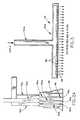
- FIG. 1is a perspective view of a reactor with a remote plasma generator system of the present invention
- FIG. 2is a cross-section taken along line II—II of FIG. 1;
- FIG. 2Ais an enlarged cross-section of the section designated IIA—IIA in FIG. 2;
- FIG. 3is an enlarged view of a gas injector tube of the reactor of FIG. 2;
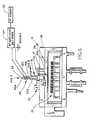
- FIG. 4is an enlarged top plan view of a cover of the reactor of FIG. 1;
- FIG. 5is an enlarged bottom plan view of the cover of FIG. 4;
- FIG. 6is a similar view to FIG. 2 illustrating a second embodiment of the remote plasma generator system of the present invention.
- FIG. 7is an enlarged view, of the remote plasma generator system of FIG. 6 .
- the numeral 10generally refers to a reactor of the present invention for processing semiconductor substrates.
- Reactor 10is suitable for performing various fabrication and treatment processes on a semiconductor substrate 12 , such as a semiconductor wafer, including thermal processing, for example thermal annealing, thermal re-flow of boro-phosphorous gases, and further chemical vapor deposition of thin film applications, such as oxide films, nitride films, doped and undoped polysilicon films, silicon epitaxial and tungsten metal and tungsten silicide films and the like, in the fabrication of semiconductor devices.
- reactor 10includes a gas injection system 16 which injects reactant gases into the reactor's processing chamber 18 for processing a substrate 12 .
- Gas injection system 16includes a plasma generator 14 for raising the level of energy of the reactant gases preferably prior to injection into chamber 18 .
- Plasma generator 14preferably ionizes reactant gases for injection into the reactor's processing chamber 18 and, more preferably, ionizes the reactant gases into a plasma, which relaxes the electron temperature and reduces the heating, and in some applications eliminates the heating, associated with most chemical vapor deposition processes.
- the stability of already deposited filmsis enhanced.
- plasma generator 14is preferably located outside reactor and ionizes the reactant gas or gases before injection into the reactor thus isolating the semiconductor substrate from the high electron energy of the plasma field which prevents changes to the substrate, such as device damage and/or failure that typically occurs when the substrate is exposed to such high electron energy.
- reactor 10includes a heater assembly 20 , which delivers heat to the substrate, preferably in a uniform manner, and an emissivity measurement assembly 22 which permits continuous emissivity measurement of the average surface area of the device side of the substrate during processing so that the amount and/or profile of the heat being delivered to the substrate during processing may be adjusted.
- a heater assembly 20which delivers heat to the substrate, preferably in a uniform manner
- an emissivity measurement assembly 22which permits continuous emissivity measurement of the average surface area of the device side of the substrate during processing so that the amount and/or profile of the heat being delivered to the substrate during processing may be adjusted.
- reactor 10includes a housing 24 which forms processing chamber 18 .
- Substrate 12is supported in processing chamber 18 on a platform 26 which is made from a suitable material, such as silicon carbide coated graphite, quartz, pure silicon carbide, alumina zirconia, aluminum, steel, or the like, and is oriented with a device side 12 a directed toward an upper wall or cover 28 of housing 24 .
- a suitable materialsuch as silicon carbide coated graphite, quartz, pure silicon carbide, alumina zirconia, aluminum, steel, or the like.
- Platform 26is preferably seated and supported in a recessed central opening 30 a provided in a top wall 30 of a second rotatable housing 32 .
- Housing 32is preferably rotatably supported in housing 24 on a base 34 .
- Base 34 and second housing 32are rotatably supported on base wall 36 of housing 24 and are preferably rotated using a conventional magnetically coupled drive mechanism 38 or other suitable driving devices which can apart rotation to base 34 through a vacuum seal.
- substrate 12is rotated to provide a uniform application of heat and reactant gases over its entire surface, as would be understood by those skilled in the art.
- the revolutions per minute (rpm) of base 34 and housing 32may be preset, for example preferably in a range of 5 to 60 rpm depending on the specific process, again is understood by those skilled in the art.
- heater assembly 20is completely enclosed by housing 32 and platform 26 , which when placed on top of housing 32 completes the enclosure of heater assembly 20 , Platform 26 can accommodate various substrate sizes, for example, substrates with diameters ranging from 150 to 300 mm and greater. Platform 26 supports substrate 12 spaced from lower surface 28 a of cover 28 with the space therebetween forming process chamber 18 .
- Process chamber 18is preferably evacuated through a vacuum exhaust port provided in gas injector assembly 16 , as will be more fully described below.
- substrate 12is placed into evacuated chamber 18 through a chamber valve 39 and is placed on platform 26 by a conventional wafer transport device (not shown), such as an automatic transport robot as is known in the art.
- gas injection assembly 16includes manifold 40 through which one or more gases are injected onto substrate 12 .
- manifold 40is formed from a plurality of gas injection tubes 46 which are arranged in a spaced relationship to extend over substrate 12 and are supported in cover 28 .
- tubes 46comprises non-reactive gas tubes, for example quartz or alumina tubes or the like.
- each gas injection tube 46is isolated from the adjacent injection tube and is aligned in a similar fashion to the channels described in commonly owned U.S. Pat. No.
- each tube 46is preferably removably supported in cover 28 so that one or more tubes 46 may be removed for cleaning or replacement.
- Gas injection manifold 40may be also assembled as a module which is positioned and supported in cover 28 so that the entire module can be removed as well as the individual tubes.
- Manifold 40also includes a gas injection ring 41 , which extends around tubes 46 and an exhaust manifold 44 , which similarly extends around tubes 46 radially inwardly of inner gas injection ring 41 .
- Injection ring 41is typically used to inject an inert gas, such as nitrogen or the like, into processing chamber 18 and directs the inert gas to the perimeter of the substrate to form a gas barrier so that when reactive gases are injected through gas injection tubes 46 the reactive gases are confined to an area of the substrate directly below the respective tubes 46 due to the placement of the vacuum exhaust manifold 44 being adjacent the gas injection tubes 46 .
- Exhaust manifold 44extends along and is adjacent gas injection tubes 46 so that any stray gas molecules which migrate near the region under exhaust manifold 44 will be exhausted from processing chamber 18 . Therefore, the gas or gases introduced by gas injection tubes are confined to a discrete volume of processing chamber 18 and, further, to a discrete area of substrate 12 .
- each tube 46includes a plurality of orifices or holes 48 , which may be formed, for example, by drilling, such as laser drilling, for directing or dispersing the respective gas in the tube onto the substrate 12 .
- the size, location, and pitch of each orifice or holemay be varied as described to vary the flow of the gas and, further, may be varied along the length of tube 46 to adjust the profile of the injected gas to optimize gas distribution over substrate 12 .
- the profile of the flow of the gasis desired to direct less gas to the center of the substrate than to the regions toward the perimeter of the substrate, as described in U.S. Pat. No. 5,814,365. In this manner, tubes 46 function similar to a sprinkler. Referring again to FIG.
- manifold 40preferably includes three tubes, a central tube 46 a and two outer tubes 46 b , 46 c .
- each tube 46 a , 46 b , or 46 cmay inject a respective gas, such as a respective reactant gas, onto substrate 12 .
- a first reactant gasmay be injected through central tube 46 a
- a second reactant gasmay be injected by tubes 46 b and 46 c .
- the flow through each tubemay be individually controlled so that they can all turn on together, be sequenced one tube after another, or a random sequence with various time intervals between each on/off cycle.
- each of the respective tubes 46 a , 46 b , 46 cmay be associated with an injection of a specific gas. It should be understood by those skilled in the art that a wide variety of gases can be employed and selectively introduced through the orifices 48 , for example hydrogen, argon, tungsten, hexaflouride, or the like to process substrate 12 .
- each tube 46 a , 46 b , 46 cincludes or is in communication with a delivery tube 50 a , 50 b , 50 c , respectively, which extends from tubes 46 a , 46 b , 46 c through cover 28 .
- Each delivery tube 50 a , 50 b , or 50 cis preferably coupled in series to a larger diameter supply tube 52 a , 52 b , or 52 c , respectively, which is positioned outside chamber 18 and above cover 28 .
- tubes 50 a , 50 b , 50 c , 46 a , 46 b , 46 cmay each have a diameter of approximately 0.25 inches with tubes 46 a , 46 b , and 46 c having orifice hole diameters of about 0.20 inches.
- Supply tubes 52 a , 52 b , and 52 ceach have a diameter in a range of 0.5 inch to 1 inch or larger.
- Supply tubes 52 a , 52 b , and 52 care also preferably formed from non-reactive material, such as quartz or alumina, and deliver ionized gases to tubes 46 a , 46 b , 46 c by way of tubes 50 a , 50 b , 50 c and, preferably, deliver gas ionized into a plasma, as will be more fully described below.
- non-reactive materialsuch as quartz or alumina
- gas injection manifold 40includes an exhaust manifold 44 .
- exhaust manifold 44extends around tubes 46 a , 46 b , 46 c to provide an additional boundary beyond which the reactive gases can not extend.
- exhaust manifold 44also assists in the prevention of back flow contamination of the reactant gases.
- exhaust manifold 44controls the film deposition on substrate 12 in a manner which results in localized area film deposition and, further, permits use of any emissivity measurement system described below.
- the gas or gases injected into chamber 18are ionized before injection so that the energy level in the gas is raised prior to injection into chamber 18 .
- the plasma generator 14is mounted exteriorly of the reactor to isolate the high electron energy from the plasma field from reaching the substrate being processed in the reactor. By isolating the plasma field, this system prevents changes in the substrate from occurring due to high electron energy which can cause device decay and failure.
- Plasma generator 14produces an electromagnetic field through which the reactant gases flow before entering supply tubes 52 a , 52 b , or 52 c .
- one or all the gasesmay be ionized before injection into chamber 18 .
- Generator 14includes a tuned cavity, such as a microwave cavity, that surrounds a tube 14 a which is inserted into the respective supply tube 52 a , 52 b , or 52 c .
- Plasma generationis affected by using a microwave generator with a suitable electrical matching network.
- This high frequency alternating poweris supplied to the tuned cavity that surrounds tube 14 a , which is preferably made of quartz or aluminum material, and in which the gas to be excited is flowing. At certain power, the flowing gas atoms become excited and even ionized depending on the power input. Excited and ionized gas atoms are then directed rapidly onto the wafer using the quartz or aluminum tubing distributor.
- the speciesreact either with another gas in the chamber and/or with the silicon wafer surface itself.
- the gaspasses through plasma generator 14 and enters supply tubes 52 a , 52 b , and 52 c , which preferably provide an enlarged passage, the respective gas ionizes and dissociates and, most preferably, ionizes into a gas plasma.
- the gas being injected into chamber 18is more reactive with the semiconductor substrate, for example silicon, germanium, or gallium arcinide and, further, the process temperatures required to achieve thin film deposition is reduced.
- reaction rateis typically about 150 Angstroms per minute.
- rate of depositionis in excess of 1,500 angstroms per minute.
- the film deposition rate of silane and ammonia at 400 mTorr and 750° C.can be achieved at around 400° C. if the reactant gases are ionized into a plasma.
- a silicon waferWhen pure oxygen gas is injected at elevated temperatures of 900° to 1,100° C., a silicon wafer can be ionized into silicon dioxide.
- silicon dioxideWhen oxygen plasma is injected into reactor 10 , silicon dioxide can be formed at the surface of a silicon wafer at temperatures as low as room temperature. Alternately, higher growth rates can be achieved when oxygen plasma is injected into chamber 18 onto a silicon wafer at or near 400° C., which is well below the 1,100° C. thermal processing conditions associated with non-ionized oxygen.
- Nitrogen gasdoes not react with a bare silicon wafer even when injected at temperatures of 1,150° C.
- nitrogenis injected in plasma form into chamber 18 onto a silicon wafer, a very thin film of silicon nitride is formed at room temperature. This deposition reaction is even further enhanced when the nitrogen is ionized using a helium plasma.
- a fluorine containing compoundfor example hydrogen Freon, NF 3 , or XeF 2 or the like
- the excited fluorine ionscan be used to etch the wafer isotropically from native oxide or deposited oxide.
- the exited fluorine ionscan be used as a very effective wafer pre-cleaning and post-deposition cleaning application.
- the use of XeF 2 as an etchantpermits pre-cleaning, etching, simultaneous etching during deposition and post-cleaning to be done at room temperature, for example 25° C.
- hydrogen plasmacan be used at various temperatures for water-surface cleaning or “pre-cleaning” for preparing the surface for gate oxide quality growth.
- silicon dioxide of high qualitycan be formed on a pre-cleaned silicon wafer.
- the formed dioxide surfacecan then be nitrided at near room temperature. This process paves the way for the formation of advanced semiconductor gate dielectrics.
- silicon nitrideis grown at temperatures less than 750° C. (which is typically the minimum processing temperature for growing silicon nitride).
- reactor 10preferably includes a non-contact emissivity measurement system 22 for measuring the emissivity and calculating the temperature of substrate 12 to one of the various fabrication processes.
- Emissivity measurement system 22determines the temperature of substrate 12 by comparing the radiation emitted by a reference light source, which is preferably positioned in the chamber 18 , with that of the radiation emitted by substrate 12 .
- the reference light sourcepreferably includes at least one lamp which is similar to construction to the lamps used in heater assembly 20 , which are described in U.S. Pat. No. 5,951,896. Reference is made to U.S. Pat. No. 5,814,365 for further details of a preferred example of the emissivity measurement system 22 .
- Reactor 10further includes a plurality of optical fiber temperature measurement probes 54 which are fixed to cover 28 and constantly collect photon density data emitted from the device side 12 a of substrate device 12 during all processing conditions.
- the temperatures measured by probes 54are sent to a main computer control to compare them to a set temperature and any deviation is computed and transformed into a control current to drive a standard off-the-shelf SCR current relay to deliver the proportional power to each of the lamp zones then the heater assembly 20 .
- reactor 10includes three probes 54 which are positioned to measure the temperature of different parts of the wafer which assures temperature uniformity during the processing cycle.
- Temperature readings of substrate 12 calculated by processing unit 56are preferably used as input into a control system (not shown) which monitors and controls the output of heater assembly 20 .
- the control systemis coupled to heater assembly 20 through an electrical feed through 58 which extends through the base wall 36 of reactor housing 24 .
- feed through 58is sealed by an O-ring or sealed using other conventional sealing devices or methods.
- lifter pins 60which protrude through platform 26 and lift substrate 12 off platform 26 for automatic loading and unloading of substrate 12 within reactor 10 .
- Lifter pins 60are raised and lowered by magnetically coupled wafer lifters 62 which are conventionally known in the art.
- Pins 56are centrally located in housing 24 and project through a central portion of the heater assembly 20 and through a central portion of platform 26 .
- lifter pins 54extend through O-ring seals provided in the base wall 36 of housing 24 .
- reactor 10includes an electromagnetic field plasma generator 114 .
- Generator 114includes a generator tube 116 , sleeve 118 which extends around generator tube 116 , and a coil 120 which extends around sleeve 118 .
- Sleeve 118preferably comprises a water-cooled sleeve to provide cooling for coil 120 .
- Coil 120is grounded on one end and electrically coupled to a drive circuit 121 .
- Drive circuit 121includes a power source 122 , such as a radio frequency (RF) power source or a microwave power source, and an impedance matching network 124 .
- RFradio frequency
- power source 122may have a frequency of 13.56 MHZ, and supply power preferably in a range of about 800-1200 watts and, more preferably, about 1000 watts.
- Coil 120is preferably a copper coil with a diameter, for example, of about 0.15 inch and is wound around sleeve 120 between about 2 and 20 turns and, more preferably, about 7 turns.
- generator tube 116includes an input end 116 a and an output end 116 b , with output end 116 b being inserted into a respective supply tube 52 a , 52 b , or 52 c .
- power supply 122is energized and coil 120 generates an electromagnetic field within generator tube 116 .
- the gasundergoes dissociation and ionization with the confines of the larger supply tube 52 a , 52 b , or 52 c .
- These “excited” gas speciesare then fed into chamber 18 and impinge onto substrate 12 .
- numerous processescan be achieved as described in the examples above.
- this remote plasma generatorsupplies energy to the gas being used to process the substrate in order to raise the energy of the gas such that the gas is ionized into a plasma form.
- Such energetic speciesthen become more chemically active and, as a result, lead to lowering the process temperatures required for the formation of semiconductor thin films with almost total isolation of the plasma generator or electric field from the wafer that is being processed.
- the remote plasma systemprevents changes in the semiconductor substrate during processing such as device damage and/or failure;
- This new quartz gas injection systemmay include one or more features as the reactor described in U.S. Pat. No.
- top or bottomand derivatives or equivalents thereof shall relate to the invention as oriented in FIGS. 1 to 7 . It is understood that the invention may assume various alternative-orientations and configurations, except where expressly specified to the contrary. It is also understood that the specific dimensions, configurations, devices and methods illustrated in the attached drawings, and described in the preceding specification, are simply exemplary embodiments of the inventive concepts defined in the appended claims. Hence, specific dimensions and other physical characteristics relating to the embodiments disclosed herein are not to be considered limiting unless the claims expressly state otherwise.
- the present inventionprovides a reactor chamber which injects reactant gases that have been transformed into a gas plasma to enhance the processing of the substrate. Furthermore, the reactor chamber delivers and controls the flow of ionized gases to the substrate during the processing so that the substrate receives a uniform deposition of thin film of the process gas or gases.
Landscapes
- Chemical & Material Sciences (AREA)
- Chemical Kinetics & Catalysis (AREA)
- Engineering & Computer Science (AREA)
- Materials Engineering (AREA)
- Mechanical Engineering (AREA)
- Metallurgy (AREA)
- Organic Chemistry (AREA)
- General Chemical & Material Sciences (AREA)
- Chemical Vapour Deposition (AREA)
- Formation Of Insulating Films (AREA)
- Drying Of Semiconductors (AREA)
Abstract
Description
Claims (42)
Priority Applications (5)
| Application Number | Priority Date | Filing Date | Title |
|---|---|---|---|
| US09/488,309US6783627B1 (en) | 2000-01-20 | 2000-01-20 | Reactor with remote plasma system and method of processing a semiconductor substrate |
| TW089119900ATW486756B (en) | 2000-01-20 | 2000-09-27 | Reactor with remote plasma system and method of processing a semiconductor substrate |
| EP00650147AEP1118691A1 (en) | 2000-01-20 | 2000-10-11 | Reactor with remote plasma system and method of processing a semiconductor substrate |
| KR1020010003037AKR20010076357A (en) | 2000-01-20 | 2001-01-19 | Reactor with remote plasma system and method of processing a semiconductor substrate |
| JP2001011166AJP2001257204A (en) | 2000-01-20 | 2001-01-19 | Substrate processing apparatus and method of manufacturing semiconductor device |
Applications Claiming Priority (1)
| Application Number | Priority Date | Filing Date | Title |
|---|---|---|---|
| US09/488,309US6783627B1 (en) | 2000-01-20 | 2000-01-20 | Reactor with remote plasma system and method of processing a semiconductor substrate |
Publications (1)
| Publication Number | Publication Date |
|---|---|
| US6783627B1true US6783627B1 (en) | 2004-08-31 |
Family
ID=23939213
Family Applications (1)
| Application Number | Title | Priority Date | Filing Date |
|---|---|---|---|
| US09/488,309Expired - LifetimeUS6783627B1 (en) | 2000-01-20 | 2000-01-20 | Reactor with remote plasma system and method of processing a semiconductor substrate |
Country Status (5)
| Country | Link |
|---|---|
| US (1) | US6783627B1 (en) |
| EP (1) | EP1118691A1 (en) |
| JP (1) | JP2001257204A (en) |
| KR (1) | KR20010076357A (en) |
| TW (1) | TW486756B (en) |
Cited By (18)
| Publication number | Priority date | Publication date | Assignee | Title |
|---|---|---|---|---|
| US20040082171A1 (en)* | 2002-09-17 | 2004-04-29 | Shin Cheol Ho | ALD apparatus and ALD method for manufacturing semiconductor device |
| US20040187779A1 (en)* | 2003-03-27 | 2004-09-30 | Park Young Hoon | Thin film deposition reactor |
| US20040235299A1 (en)* | 2003-05-22 | 2004-11-25 | Axcelis Technologies, Inc. | Plasma ashing apparatus and endpoint detection process |
| US20040238123A1 (en)* | 2003-05-22 | 2004-12-02 | Axcelis Technologies, Inc. | Plasma apparatus, gas distribution assembly for a plasma apparatus and processes therewith |
| US20060006057A1 (en)* | 2002-06-28 | 2006-01-12 | Robert Bosch Gmbh | Device and method for the production of chlorotriflouride and system for etching semiconductor substrates using said device |
| US20070116892A1 (en)* | 2005-11-18 | 2007-05-24 | Daystar Technologies, Inc. | Methods and apparatus for treating a work piece with a vaporous element |
| US20100078045A1 (en)* | 2008-09-29 | 2010-04-01 | Toratani Kenichiro | Semiconductor manufacturing apparatus and method for cleaning same |
| US20140099794A1 (en)* | 2012-09-21 | 2014-04-10 | Applied Materials, Inc. | Radical chemistry modulation and control using multiple flow pathways |
| US20140238608A1 (en)* | 2013-02-28 | 2014-08-28 | Novellus Systems, Inc. | Ceramic showerhead with embedded rf electrode for capacitively coupled plasma reactor |
| US20150118416A1 (en)* | 2013-10-31 | 2015-04-30 | Semes Co., Ltd. | Substrate treating apparatus and method |
| US20150167161A1 (en)* | 2012-06-07 | 2015-06-18 | Soitec | Gas injection components for deposition systems and related methods |
| US9129778B2 (en) | 2011-03-18 | 2015-09-08 | Lam Research Corporation | Fluid distribution members and/or assemblies |
| CN109155251A (en)* | 2016-05-19 | 2019-01-04 | 应用材料公司 | For the conductor etching of improvement and the System and method for of component protection |
| US10224182B2 (en) | 2011-10-17 | 2019-03-05 | Novellus Systems, Inc. | Mechanical suppression of parasitic plasma in substrate processing chamber |
| US10342110B1 (en)* | 2018-09-14 | 2019-07-02 | Serendipity Technologies LLC. | Plasma power generator (z-box and z-tower) |
| US10879049B2 (en)* | 2015-07-30 | 2020-12-29 | Taiwan Semiconductor Manufacturing Co., Ltd. | Chemical vapor deposition tool and operating method thereof |
| US12009228B2 (en) | 2015-02-03 | 2024-06-11 | Applied Materials, Inc. | Low temperature chuck for plasma processing systems |
| DE102023105638A1 (en) | 2023-03-07 | 2024-09-12 | VON ARDENNE Asset GmbH & Co. KG | Chamber lid and vacuum chamber |
Families Citing this family (7)
| Publication number | Priority date | Publication date | Assignee | Title |
|---|---|---|---|---|
| DE10320597A1 (en)* | 2003-04-30 | 2004-12-02 | Aixtron Ag | Method and device for depositing semiconductor layers with two process gases, one of which is preconditioned |
| US20060062914A1 (en)* | 2004-09-21 | 2006-03-23 | Diwakar Garg | Apparatus and process for surface treatment of substrate using an activated reactive gas |
| WO2007035460A1 (en)* | 2005-09-20 | 2007-03-29 | Air Products And Chemicals, Inc. | Apparatus and process for surface treatment of substrate using an activated reactive gas |
| US8372203B2 (en)* | 2005-09-30 | 2013-02-12 | Applied Materials, Inc. | Apparatus temperature control and pattern compensation |
| DE102009043840A1 (en) | 2009-08-24 | 2011-03-03 | Aixtron Ag | CVD reactor with strip-like gas inlet zones and method for depositing a layer on a substrate in such a CVD reactor |
| US10453657B2 (en) | 2016-07-08 | 2019-10-22 | Applied Materials, Inc. | Apparatus for depositing metal films with plasma treatment |
| JP2022097945A (en)* | 2020-12-21 | 2022-07-01 | 株式会社アルバック | Substrate processing device and substrate processing method |
Citations (26)
| Publication number | Priority date | Publication date | Assignee | Title |
|---|---|---|---|---|
| JPS56102577A (en)* | 1980-01-18 | 1981-08-17 | Mitsubishi Electric Corp | Method and device for forming thin film |
| US4540868A (en) | 1982-03-06 | 1985-09-10 | Deutsche Forschungs- Und Versuchsanstalt Fur Luft- Und Raumfahrt E.V. | Plasma gun that reduces cathode contamination |
| US4550684A (en) | 1983-08-11 | 1985-11-05 | Genus, Inc. | Cooled optical window for semiconductor wafer heating |
| US4596718A (en) | 1984-06-19 | 1986-06-24 | Plasmainvent Ag | Vacuum plasma coating apparatus |
| US4680447A (en) | 1983-08-11 | 1987-07-14 | Genus, Inc. | Cooled optical window for semiconductor wafer heating |
| US4942058A (en) | 1986-04-15 | 1990-07-17 | Canon Kabushiki Kaisha | Process for forming deposited film |
| US4993358A (en) | 1989-07-28 | 1991-02-19 | Watkins-Johnson Company | Chemical vapor deposition reactor and method of operation |
| US5155336A (en) | 1990-01-19 | 1992-10-13 | Applied Materials, Inc. | Rapid thermal heating apparatus and method |
| JPH05139881A (en) | 1991-11-18 | 1993-06-08 | Sumitomo Electric Ind Ltd | Molecular beam epitaxial growth method and its equipment |
| US5310260A (en) | 1990-04-10 | 1994-05-10 | Luxtron Corporation | Non-contact optical techniques for measuring surface conditions |
| US5366002A (en) | 1993-05-05 | 1994-11-22 | Applied Materials, Inc. | Apparatus and method to ensure heat transfer to and from an entire substrate during semiconductor processing |
| FR2715168A1 (en) | 1994-01-14 | 1995-07-21 | Univ Lille Sciences Tech | Method for depositing, at room temperature, a layer of metal or semi-metal and their oxide on a substrate. |
| US5453124A (en) | 1992-12-30 | 1995-09-26 | Texas Instruments Incorporated | Programmable multizone gas injector for single-wafer semiconductor processing equipment |
| US5487787A (en) | 1991-05-10 | 1996-01-30 | Celestech, Inc. | Apparatus and method for plasma deposition |
| US5531835A (en) | 1994-05-18 | 1996-07-02 | Applied Materials, Inc. | Patterned susceptor to reduce electrostatic force in a CVD chamber |
| JPH0964307A (en) | 1995-08-29 | 1997-03-07 | Hitachi Ltd | Heat treatment method for oxide thin film |
| JPH0969504A (en) | 1994-07-21 | 1997-03-11 | Applied Komatsu Technol Kk | Cleaning technology for deposition chamber employing remote exciting source |
| JPH09219295A (en) | 1996-01-30 | 1997-08-19 | Applied Materials Inc | Liquid-cooled remote plasma applicator |
| US5788778A (en)* | 1996-09-16 | 1998-08-04 | Applied Komatsu Technology, Inc. | Deposition chamber cleaning technique using a high power remote excitation source |
| US5814365A (en)* | 1997-08-15 | 1998-09-29 | Micro C Technologies, Inc. | Reactor and method of processing a semiconductor substate |
| US5916455A (en)* | 1996-03-18 | 1999-06-29 | Applied Materials, Inc. | Method and apparatus for generating a low pressure plasma |
| JPH11187253A (en) | 1997-12-22 | 1999-07-09 | Canon Inc | Image processing apparatus and method |
| US5948168A (en)* | 1995-06-23 | 1999-09-07 | Applied Materials, Inc. | Distributed microwave plasma reactor for semiconductor processing |
| US6225745B1 (en)* | 1999-12-17 | 2001-05-01 | Axcelis Technologies, Inc. | Dual plasma source for plasma process chamber |
| US6263831B1 (en)* | 1998-02-17 | 2001-07-24 | Dry Plasma Systems, Inc. | Downstream plasma using oxygen gas mixtures |
| US6283130B1 (en)* | 1995-05-30 | 2001-09-04 | Anelva Corporation | Plasma cleaning method and placement area protector used in the method |
Family Cites Families (1)
| Publication number | Priority date | Publication date | Assignee | Title |
|---|---|---|---|---|
| US5976992A (en)* | 1993-09-27 | 1999-11-02 | Kabushiki Kaisha Toshiba | Method of supplying excited oxygen |
- 2000
- 2000-01-20USUS09/488,309patent/US6783627B1/ennot_activeExpired - Lifetime
- 2000-09-27TWTW089119900Apatent/TW486756B/enactive
- 2000-10-11EPEP00650147Apatent/EP1118691A1/ennot_activeWithdrawn
- 2001
- 2001-01-19JPJP2001011166Apatent/JP2001257204A/enactivePending
- 2001-01-19KRKR1020010003037Apatent/KR20010076357A/ennot_activeCeased
Patent Citations (31)
| Publication number | Priority date | Publication date | Assignee | Title |
|---|---|---|---|---|
| JPS56102577A (en)* | 1980-01-18 | 1981-08-17 | Mitsubishi Electric Corp | Method and device for forming thin film |
| US4540868A (en) | 1982-03-06 | 1985-09-10 | Deutsche Forschungs- Und Versuchsanstalt Fur Luft- Und Raumfahrt E.V. | Plasma gun that reduces cathode contamination |
| US4550684A (en) | 1983-08-11 | 1985-11-05 | Genus, Inc. | Cooled optical window for semiconductor wafer heating |
| US4680447A (en) | 1983-08-11 | 1987-07-14 | Genus, Inc. | Cooled optical window for semiconductor wafer heating |
| US4596718A (en) | 1984-06-19 | 1986-06-24 | Plasmainvent Ag | Vacuum plasma coating apparatus |
| US4596718B1 (en) | 1984-06-19 | 1989-10-17 | ||
| US4942058A (en) | 1986-04-15 | 1990-07-17 | Canon Kabushiki Kaisha | Process for forming deposited film |
| US4993358A (en) | 1989-07-28 | 1991-02-19 | Watkins-Johnson Company | Chemical vapor deposition reactor and method of operation |
| US5155336A (en) | 1990-01-19 | 1992-10-13 | Applied Materials, Inc. | Rapid thermal heating apparatus and method |
| US5317492A (en) | 1990-01-19 | 1994-05-31 | Applied Materials, Inc. | Rapid thermal heating apparatus and method |
| US5487127A (en) | 1990-01-19 | 1996-01-23 | Applied Materials, Inc. | Rapid thermal heating apparatus and method utilizing plurality of light pipes |
| US5310260A (en) | 1990-04-10 | 1994-05-10 | Luxtron Corporation | Non-contact optical techniques for measuring surface conditions |
| US5490728A (en) | 1990-04-10 | 1996-02-13 | Luxtron Corporation | Non-contact optical techniques for measuring surface conditions |
| US5487787A (en) | 1991-05-10 | 1996-01-30 | Celestech, Inc. | Apparatus and method for plasma deposition |
| JPH05139881A (en) | 1991-11-18 | 1993-06-08 | Sumitomo Electric Ind Ltd | Molecular beam epitaxial growth method and its equipment |
| US5453124A (en) | 1992-12-30 | 1995-09-26 | Texas Instruments Incorporated | Programmable multizone gas injector for single-wafer semiconductor processing equipment |
| US5366002A (en) | 1993-05-05 | 1994-11-22 | Applied Materials, Inc. | Apparatus and method to ensure heat transfer to and from an entire substrate during semiconductor processing |
| US5566744A (en) | 1993-05-05 | 1996-10-22 | Applied Materials, Inc. | Apparatus and method to ensure heat transfer to and from an entire substrate during semiconductor processing |
| FR2715168A1 (en) | 1994-01-14 | 1995-07-21 | Univ Lille Sciences Tech | Method for depositing, at room temperature, a layer of metal or semi-metal and their oxide on a substrate. |
| US5531835A (en) | 1994-05-18 | 1996-07-02 | Applied Materials, Inc. | Patterned susceptor to reduce electrostatic force in a CVD chamber |
| JPH0969504A (en) | 1994-07-21 | 1997-03-11 | Applied Komatsu Technol Kk | Cleaning technology for deposition chamber employing remote exciting source |
| US6283130B1 (en)* | 1995-05-30 | 2001-09-04 | Anelva Corporation | Plasma cleaning method and placement area protector used in the method |
| US5948168A (en)* | 1995-06-23 | 1999-09-07 | Applied Materials, Inc. | Distributed microwave plasma reactor for semiconductor processing |
| JPH0964307A (en) | 1995-08-29 | 1997-03-07 | Hitachi Ltd | Heat treatment method for oxide thin film |
| JPH09219295A (en) | 1996-01-30 | 1997-08-19 | Applied Materials Inc | Liquid-cooled remote plasma applicator |
| US5916455A (en)* | 1996-03-18 | 1999-06-29 | Applied Materials, Inc. | Method and apparatus for generating a low pressure plasma |
| US5788778A (en)* | 1996-09-16 | 1998-08-04 | Applied Komatsu Technology, Inc. | Deposition chamber cleaning technique using a high power remote excitation source |
| US5814365A (en)* | 1997-08-15 | 1998-09-29 | Micro C Technologies, Inc. | Reactor and method of processing a semiconductor substate |
| JPH11187253A (en) | 1997-12-22 | 1999-07-09 | Canon Inc | Image processing apparatus and method |
| US6263831B1 (en)* | 1998-02-17 | 2001-07-24 | Dry Plasma Systems, Inc. | Downstream plasma using oxygen gas mixtures |
| US6225745B1 (en)* | 1999-12-17 | 2001-05-01 | Axcelis Technologies, Inc. | Dual plasma source for plasma process chamber |
Non-Patent Citations (1)
| Title |
|---|
| Search Report on European Patent Application No. EP 00 65 0147, which corresponds to U.S. patent application Ser. No. 09/488,309. |
Cited By (32)
| Publication number | Priority date | Publication date | Assignee | Title |
|---|---|---|---|---|
| US8382940B2 (en)* | 2002-06-28 | 2013-02-26 | Robert Bosch Gmbh | Device and method for producing chlorine trifluoride and system for etching semiconductor substrates using this device |
| US20060006057A1 (en)* | 2002-06-28 | 2006-01-12 | Robert Bosch Gmbh | Device and method for the production of chlorotriflouride and system for etching semiconductor substrates using said device |
| US7435445B2 (en)* | 2002-09-17 | 2008-10-14 | Moohan Co., Ltd. | Method for manufacturing semiconductor device |
| US20040082171A1 (en)* | 2002-09-17 | 2004-04-29 | Shin Cheol Ho | ALD apparatus and ALD method for manufacturing semiconductor device |
| US20060177579A1 (en)* | 2002-09-17 | 2006-08-10 | Shin Cheol H | Method for manufacturing semiconductor device |
| US20040187779A1 (en)* | 2003-03-27 | 2004-09-30 | Park Young Hoon | Thin film deposition reactor |
| US20100055807A1 (en)* | 2003-05-22 | 2010-03-04 | Axcelis Technologies, Inc. | Plasma ashing apparatus and endpoint detection process |
| US20040235299A1 (en)* | 2003-05-22 | 2004-11-25 | Axcelis Technologies, Inc. | Plasma ashing apparatus and endpoint detection process |
| US8580076B2 (en)* | 2003-05-22 | 2013-11-12 | Lam Research Corporation | Plasma apparatus, gas distribution assembly for a plasma apparatus and processes therewith |
| US20040238123A1 (en)* | 2003-05-22 | 2004-12-02 | Axcelis Technologies, Inc. | Plasma apparatus, gas distribution assembly for a plasma apparatus and processes therewith |
| US8268181B2 (en) | 2003-05-22 | 2012-09-18 | Axcelis Technologies, Inc. | Plasma ashing apparatus and endpoint detection process |
| US7442413B2 (en) | 2005-11-18 | 2008-10-28 | Daystar Technologies, Inc. | Methods and apparatus for treating a work piece with a vaporous element |
| US20070116892A1 (en)* | 2005-11-18 | 2007-05-24 | Daystar Technologies, Inc. | Methods and apparatus for treating a work piece with a vaporous element |
| US20070116893A1 (en)* | 2005-11-18 | 2007-05-24 | Daystar Technologies, Inc. | Low-hydrogen photovoltaic cell |
| US20100078045A1 (en)* | 2008-09-29 | 2010-04-01 | Toratani Kenichiro | Semiconductor manufacturing apparatus and method for cleaning same |
| US9566620B2 (en) | 2008-09-29 | 2017-02-14 | Kabushiki Kaisha Toshiba | Semiconductor manufacturing apparatus and method for cleaning same |
| US9129778B2 (en) | 2011-03-18 | 2015-09-08 | Lam Research Corporation | Fluid distribution members and/or assemblies |
| US11621150B2 (en) | 2011-10-17 | 2023-04-04 | Lam Research Corporation | Mechanical suppression of parasitic plasma in substrate processing chamber |
| US10224182B2 (en) | 2011-10-17 | 2019-03-05 | Novellus Systems, Inc. | Mechanical suppression of parasitic plasma in substrate processing chamber |
| US20150167161A1 (en)* | 2012-06-07 | 2015-06-18 | Soitec | Gas injection components for deposition systems and related methods |
| US20140099794A1 (en)* | 2012-09-21 | 2014-04-10 | Applied Materials, Inc. | Radical chemistry modulation and control using multiple flow pathways |
| US20140238608A1 (en)* | 2013-02-28 | 2014-08-28 | Novellus Systems, Inc. | Ceramic showerhead with embedded rf electrode for capacitively coupled plasma reactor |
| US9449795B2 (en)* | 2013-02-28 | 2016-09-20 | Novellus Systems, Inc. | Ceramic showerhead with embedded RF electrode for capacitively coupled plasma reactor |
| US20150118416A1 (en)* | 2013-10-31 | 2015-04-30 | Semes Co., Ltd. | Substrate treating apparatus and method |
| US12009228B2 (en) | 2015-02-03 | 2024-06-11 | Applied Materials, Inc. | Low temperature chuck for plasma processing systems |
| US10879049B2 (en)* | 2015-07-30 | 2020-12-29 | Taiwan Semiconductor Manufacturing Co., Ltd. | Chemical vapor deposition tool and operating method thereof |
| CN109155251A (en)* | 2016-05-19 | 2019-01-04 | 应用材料公司 | For the conductor etching of improvement and the System and method for of component protection |
| CN109155251B (en)* | 2016-05-19 | 2023-08-15 | 应用材料公司 | Systems and methods for improved semiconductor etching and component protection |
| US10342110B1 (en)* | 2018-09-14 | 2019-07-02 | Serendipity Technologies LLC. | Plasma power generator (z-box and z-tower) |
| US20200092976A1 (en)* | 2018-09-14 | 2020-03-19 | Amen Dhyllon | PLASMA POWER GENERATOR (Z-box and Z-tower) |
| US10869379B2 (en)* | 2018-09-14 | 2020-12-15 | Serendipity Technologies Llc | Plasma power generator (Z-box and Z-tower) |
| DE102023105638A1 (en) | 2023-03-07 | 2024-09-12 | VON ARDENNE Asset GmbH & Co. KG | Chamber lid and vacuum chamber |
Also Published As
| Publication number | Publication date |
|---|---|
| TW486756B (en) | 2002-05-11 |
| KR20010076357A (en) | 2001-08-11 |
| JP2001257204A (en) | 2001-09-21 |
| EP1118691A1 (en) | 2001-07-25 |
Similar Documents
| Publication | Publication Date | Title |
|---|---|---|
| US6783627B1 (en) | Reactor with remote plasma system and method of processing a semiconductor substrate | |
| US6800830B2 (en) | Chemistry for boron diffusion barrier layer and method of application in semiconductor device fabrication | |
| US7816205B2 (en) | Method of forming non-volatile memory having charge trap layer with compositional gradient | |
| US5015330A (en) | Film forming method and film forming device | |
| JP4994551B2 (en) | Improved apparatus and method for growing thin films | |
| US20060029747A1 (en) | Elimination of flow and pressure gradients in low utilization processes | |
| CN101310036B (en) | Multi-layer high-quality gate dielectric layer for low-temperature polysilicon TFT | |
| JP5698719B2 (en) | In-situ chamber cleaning process to remove byproduct deposits from chemical vapor deposition etch chambers | |
| TWI557799B (en) | Method for oxidizing a semiconductor device | |
| US7588036B2 (en) | Chamber clean method using remote and in situ plasma cleaning systems | |
| US20040086434A1 (en) | Apparatus and method for treating objects with radicals generated from plasma | |
| KR101991574B1 (en) | Film forming apparatus and gas injection member user therefor | |
| EP1067587B1 (en) | Thermally processing a substrate | |
| KR20060042255A (en) | In-Shot Dry Cleaning Chamber for FOE Production | |
| KR20050010782A (en) | Method for improving nitrogen profile in plasma nitrided gate dielectric layers | |
| JP2004349546A (en) | Oxide film forming method, oxide film forming apparatus and electronic device material | |
| KR101994164B1 (en) | Sealing film forming method | |
| JP6937806B2 (en) | Substrate processing equipment and semiconductor manufacturing method | |
| KR20000062563A (en) | Method and apparatus for forming material layers from atomic gasses | |
| US20230053083A1 (en) | Plasma processing apparatus and film forming method | |
| KR101579504B1 (en) | Method of manufacturing semiconductor device, method of processing substrate, substrate processing apparatus and non-transitory computer-readable recording medium | |
| JP3129777B2 (en) | Heat treatment apparatus and heat treatment method | |
| JPH06196410A (en) | Plasma processing device | |
| JP2005259902A (en) | Substrate processing equipment | |
| KR102688353B1 (en) | Apparatus and method for treating substrate |
Legal Events
| Date | Code | Title | Description |
|---|---|---|---|
| AS | Assignment | Owner name:MICRO C TECHNOLOGIES, INC., MICHIGAN Free format text:ASSIGNMENT OF ASSIGNORS INTEREST;ASSIGNOR:MAHAWILI, IMAD;REEL/FRAME:010573/0075 Effective date:20000119 | |
| AS | Assignment | Owner name:KOKUSAI SEMICONDUCTOR EQUIPMENT CORPORATION, CALIF Free format text:ASSIGNMENT OF ASSIGNORS INTEREST;ASSIGNOR:MICRO C TECHNOLOGIES, INC.;REEL/FRAME:014709/0282 Effective date:20031110 | |
| STCF | Information on status: patent grant | Free format text:PATENTED CASE | |
| CC | Certificate of correction | ||
| FEPP | Fee payment procedure | Free format text:PAT HOLDER NO LONGER CLAIMS SMALL ENTITY STATUS, ENTITY STATUS SET TO UNDISCOUNTED (ORIGINAL EVENT CODE: STOL); ENTITY STATUS OF PATENT OWNER: LARGE ENTITY | |
| REFU | Refund | Free format text:REFUND - SURCHARGE, PETITION TO ACCEPT PYMT AFTER EXP, UNINTENTIONAL (ORIGINAL EVENT CODE: R2551); ENTITY STATUS OF PATENT OWNER: LARGE ENTITY | |
| FPAY | Fee payment | Year of fee payment:4 | |
| FPAY | Fee payment | Year of fee payment:8 | |
| FPAY | Fee payment | Year of fee payment:12 | |
| IPR | Aia trial proceeding filed before the patent and appeal board: inter partes review | Free format text:TRIAL NO: IPR2018-01582 Opponent name:ASM IP HOLDING B.V. Effective date:20180822 Free format text:TRIAL NO: IPR2018-01584 Opponent name:ASM IP HOLDING B.V. Effective date:20180822 |