US6781317B1 - Methods and apparatus for calibration and metrology for an integrated RF generator system - Google Patents
Methods and apparatus for calibration and metrology for an integrated RF generator systemDownload PDFInfo
- Publication number
- US6781317B1 US6781317B1US10/373,163US37316303AUS6781317B1US 6781317 B1US6781317 B1US 6781317B1US 37316303 AUS37316303 AUS 37316303AUS 6781317 B1US6781317 B1US 6781317B1
- Authority
- US
- United States
- Prior art keywords
- load
- signal
- matching network
- calibration
- impedance matching
- Prior art date
- Legal status (The legal status is an assumption and is not a legal conclusion. Google has not performed a legal analysis and makes no representation as to the accuracy of the status listed.)
- Expired - Lifetime
Links
- 238000000034methodMethods0.000titleclaimsabstractdescription74
- 239000000523sampleSubstances0.000claimsabstractdescription61
- 238000004891communicationMethods0.000claimsabstractdescription12
- 238000003860storageMethods0.000claimsabstractdescription4
- 238000005259measurementMethods0.000claimsdescription20
- 239000003990capacitorSubstances0.000claimsdescription11
- 230000008569processEffects0.000claimsdescription8
- 238000012544monitoring processMethods0.000claimsdescription5
- 238000004519manufacturing processMethods0.000claimsdescription4
- 238000010521absorption reactionMethods0.000claimsdescription2
- 238000013500data storageMethods0.000claimsdescription2
- 230000037361pathwayEffects0.000claimsdescription2
- 238000010586diagramMethods0.000description13
- 238000012545processingMethods0.000description11
- 239000000758substrateSubstances0.000description7
- 230000001939inductive effectEffects0.000description6
- 238000007707calorimetryMethods0.000description4
- 230000008859changeEffects0.000description4
- 239000007789gasSubstances0.000description3
- 230000004044responseEffects0.000description3
- XKRFYHLGVUSROY-UHFFFAOYSA-NArgonChemical compound[Ar]XKRFYHLGVUSROY-UHFFFAOYSA-N0.000description2
- 239000002826coolantSubstances0.000description2
- 230000001419dependent effectEffects0.000description2
- 239000000463materialSubstances0.000description2
- 239000004065semiconductorSubstances0.000description2
- PNEYBMLMFCGWSK-UHFFFAOYSA-Naluminium oxideInorganic materials[O-2].[O-2].[O-2].[Al+3].[Al+3]PNEYBMLMFCGWSK-UHFFFAOYSA-N0.000description1
- 238000013459approachMethods0.000description1
- 229910052786argonInorganic materials0.000description1
- 230000005540biological transmissionEffects0.000description1
- 239000000919ceramicSubstances0.000description1
- 239000013626chemical specieSubstances0.000description1
- 238000004140cleaningMethods0.000description1
- 238000001816coolingMethods0.000description1
- 230000008021depositionEffects0.000description1
- 238000013461designMethods0.000description1
- 230000000694effectsEffects0.000description1
- 230000005672electromagnetic fieldEffects0.000description1
- 238000005516engineering processMethods0.000description1
- 238000005530etchingMethods0.000description1
- 230000003993interactionEffects0.000description1
- 239000007788liquidSubstances0.000description1
- 238000012986modificationMethods0.000description1
- 230000004048modificationEffects0.000description1
- 150000004767nitridesChemical class0.000description1
- 238000011017operating methodMethods0.000description1
- 239000002245particleSubstances0.000description1
- -1pressureSubstances0.000description1
- 238000013064process characterizationMethods0.000description1
- 238000004886process controlMethods0.000description1
- 238000011002quantificationMethods0.000description1
- 238000012546transferMethods0.000description1
- 230000009466transformationEffects0.000description1
- 230000001131transforming effectEffects0.000description1
- 238000013024troubleshootingMethods0.000description1
Images


Classifications
- H—ELECTRICITY
- H01—ELECTRIC ELEMENTS
- H01J—ELECTRIC DISCHARGE TUBES OR DISCHARGE LAMPS
- H01J37/00—Discharge tubes with provision for introducing objects or material to be exposed to the discharge, e.g. for the purpose of examination or processing thereof
- H01J37/32—Gas-filled discharge tubes
- H01J37/32917—Plasma diagnostics
- H01J37/32935—Monitoring and controlling tubes by information coming from the object and/or discharge
- H—ELECTRICITY
- H01—ELECTRIC ELEMENTS
- H01J—ELECTRIC DISCHARGE TUBES OR DISCHARGE LAMPS
- H01J37/00—Discharge tubes with provision for introducing objects or material to be exposed to the discharge, e.g. for the purpose of examination or processing thereof
- H01J37/32—Gas-filled discharge tubes
- H01J37/32009—Arrangements for generation of plasma specially adapted for examination or treatment of objects, e.g. plasma sources
- H01J37/32082—Radio frequency generated discharge
Definitions
- the present inventionrelates generally to plasma processing equipment.
- the present inventionrelates to calibration and control of RF and microwave plasma processing equipment.
- Radio frequency or microwave (hereinafter “RF”) plasma generation equipmentis widely used in semiconductor and industrial plasma processing.
- Plasma processingsupports a wide variety of applications, including etching of materials from substrates, deposition of materials onto substrates, cleaning of substrate surfaces, and modification of substrate surfaces.
- the frequency and power levels employedvary widely, from about 10 kHz to 2.45 GHz and from a few Watts to as much as 100 kW or greater.
- the range of frequencies and powers presently used in plasma processing equipmentis somewhat narrower, ranging from about 10 KHz to 2.45 GHz and 10 W to 30 kW, respectively.
- Plasma processing equipmenttypically requires a precision RF signal generator, a matching network, cabling, and metrology equipment.
- precision instrumentationis usually required to control the actual power reaching the plasma.
- the impedance of loads associated with a plasmacan vary considerably in response to variations in gas recipe, plasma density, delivered RF power, pressure and other parameters.
- An RF supplyincluding a signal generator and matching network, can deliver power to the plasma in a number of ways, for example, via an antenna or sample holder.
- An antennatypically has a primarily inductive load impedance, with a smaller resistive component.
- a sample holdertypically presents a primarily capacitive impedance, also with a smaller resistive component.
- Matching networksare typically positioned between the output of the RF generator and the input of the process chamber.
- the matching networkprovides a means of matching the output impedance of the generator to the input impedance of the process chamber.
- a matching networkoften includes elements such as variable capacitors and variable inductors to permit dynamic impedance matching of an RF generator to a changing load.
- a matching networkcan accommodate mismatches in impedance between the standard fifty-ohm output impedance of the RF generator and the input of the load. The mismatch can be exacerbated by a process chamber and plasma whose associated load can fluctuate over a large range of values.
- the impedance mismatchcan cause inefficient power deliver.
- the mismatchcan also cause the power delivered to the plasma to vary, which can cause process inconsistency both within a chamber for successive substrates and among similar chambers.
- use of an impedance matching networkcan improve the efficiency of power transfer from a signal generator to a plasma vessel.
- Components used in some plasma generation systemscan present further difficulties in process characterization and control.
- many systemsutilize coaxial cables to connect an RF generator to an impedance matching network.
- Determination of the power delivered to a reactive loadcan be difficult and of limited accuracy.
- a standard operating methodentails holding power delivered to the plasma vessel load constant.
- the poweris generally not well known because, for example, power is lost in the matchbox; the lost power is a complicated function of, for example, the positions of the vacuum variable capacitors in a matchbox plus a plasma vessel load having a nonlinear behavior.
- An impedance probecan be placed between the matchbox and the plasma vessel to obtain a measure of power delivered to the plasma vessel.
- This approachhas at least two disadvantages. First, an impedance probe can be very inaccurate when the phase angle between current voltage waveforms is high. A high phase angle typically is encountered for a highly reactive plasma vessel load. Second, impedance probes are typically too costly for production systems.
- An RF plasma generation systemcan include an RF generator, impedance matching network, a signal probe that monitors the RF signal between the generator and the matching network, a plasma vessel, and a calibration database.
- the calibration databaseprovides data that permits accurate determination, for example, of plasma vessel power consumption via RF signal parameter values collected by the signal probe.
- the calibration databaseis obtained from measurements collected from the impedance matching network and a calibration load that represents the behavior of the plasma vessel.
- the systemcan provide accurate measurements of plasma vessel impedance and plasma vessel power consumption, even when the load associated with the plasma vessel is highly reactive.
- the systemis particularly well suited to designs that include a variable frequency RF generator and an impedance matching network having an impedance that is fixed during operation of the system. In such a system, the frequency can be adjusted to obtain a minimum in reflected power.
- the inventionfeatures a method for operating an RF plasma generation system.
- the systemcan include an RF signal generator, an impedance matching network, a plasma vessel, and an RF signal probe that monitors the RF signal delivered from the RF signal generator to an input port of the impedance matching network.
- the methodincludes causing an RF signal to be applied to the input port of the impedance matching network, monitoring a present value of at least one parameter of the RF signal associated with the input port of the impedance matching network, and causing the RF signal to be applied from an output port of the impedance matching network to an input port of the plasma vessel.
- the RF signalis monitored at a location along a pathway of the RF signal between the RF signal generator and the input port of the impedance matching network.
- the methodalso includes providing calibration data associating values of the RF signal parameter with values of a characteristic of a load associated with the plasma vessel.
- a present value of the characteristic of the load associated with the present value of the parameter of the RF signalis determined by referencing the calibration data.
- the impedance matching networkhas a fixed impedance.
- the impedance matching networkcan have a plurality of fixed impedances associated with a plurality of operating recipes of the RF plasma generation system.
- the inventionfeatures a method for calibrating an RF plasma generation system.
- the methodincludes providing a calibration load that represents the load associated with the plasma vessel.
- the calibration loadhas an input port in electromagnetic communication with an output port of the impedance matching network.
- a sequence of RF signalsis applied to the input port of the impedance matching network thereby causing the sequence of RF signals to be applied to an input port of the calibration load.
- At least one parameter associated with the sequence of RF signals applied to the input port of the impedance matching networkis determined, as is at least one characteristic of the calibration load responsive to the sequence of RF signals.
- the power of the RF signalscan be ramped over a range of power values associated with operation of the RF plasma generating system.
- a value of the impedance of the calibration loadcan be determined to characterize the calibration load, and the value of the impedance can be stored.
- At least one value of the impedance of the load, associated with a center frequency of the RF signal, a range of frequencies of the RF signal, and/or a range of temperatures of the calibration load,can be determined.
- the characteristic of the calibration loadcan be a power consumption of the calibration load.
- the inventionfeatures an RF plasma generation system.
- the systemincludes an impedance matching network having an input port to receive an RF signal from an RF generator, and an output port to deliver the RF signal to an input port of a plasma vessel associated with a load.
- the systemincludes an RF signal probe in electromagnetic communication with the input port of the impedance matching network to detect at least one RF signal parameter associated with the RF signal at the input port of the impedance matching network.
- the systemalso includes a calibration storage unit.
- the unitstores calibration data that includes an association of values of the RF signal parameter with values of at least one characteristic of the load.
- a control unitdetermines an association between the detected signal parameter and a present value of the plasma vessel load characteristic by referencing the calibration data.
- the inventionfeatures an RF plasma generation system.
- the systemincludes an impedance matching network, a plasma vessel associated with a load, and a data storage unit storing calibration data.
- the calibration datais created by a method that includes providing a calibration load that represents the load associated with the plasma vessel.
- the calibration loadhas an input port in electromagnetic communication with an output port of the impedance matching network.
- the methodincludes applying a sequence of RF signals to the input port of the impedance matching network, determining at least one parameter associated with the sequence of RF signals applied to the input port of the impedance matching network, and determining at least one characteristic of the calibration load responsive to the sequence of RF signals.
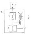
- FIG. 1is a block diagram of an embodiment of an RF plasma generation system.
- FIG. 2is an embodiment of an equivalent circuit diagram, which is associated with the matching network and the plasma vessel of FIG. 1 .
- FIG. 3is a flowchart of an embodiment of a method for operating an RF plasma generation system.
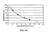
- FIG. 4 ais a graph of a curve that relates load resistance values to reflection coefficient values for one operational embodiment of an RF plasma generation system.
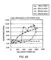
- FIGS. 4 b , 4 c and 4 dare graphs of exemplary calibration data, which illustrate specific operational recipes for an embodiment of an RF plasma generation system.
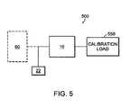
- FIG. 5is a block diagram of an embodiment of a calibration apparatus.
- FIG. 6is a block diagram of an embodiment of a calibration load.
- FIGS. 7 a and 7 bare block diagrams of embodiments of calibration apparatus for calibrating a calibration load.
- FIG. 8is a flowchart of an embodiment of a method for calibration of an RF plasma generation system.
- An “RF signal”, as used herein,refers to an electromagnetic field or a collection of moving charged particles having a frequency in the RF or microwave range.
- an RF generatorproduces an RF signal for delivery, for example, to a matching network. After transforming the RF signal, the network can provide the RF signal for delivery to a plasma vessel.
- a “plasma vessel”includes at least one RF delivery component and has at least one chamber within which a plasma can exist.
- An “RF delivery component”can deliver power to a plasma in a chamber of a plasma vessel.
- the RF delivery componentcan be, for example, a chuck and/or a coil.
- a “coil”is a predominately inductive antenna component of a plasma vessel, which delivers power to a plasma within the vessel.
- a “chuck” or “bias”is a predominately capacitive component of a plasma vessel, which delivers RF power to a plasma within the vessel.
- a chuck or biascan be a sample substrate holder.
- a “load”is, or relates to, a component or portion of a plasma system that consumes power (for example, a plasma vessel load).
- a loadcan be characterized by an impedance associated with the load. Information about the impedance can assist in determination of the power consumed by the load.
- a “plasma vessel load”(also referred to as a load or impedance associated with a plasma vessel) is primarily a combination of the load associated with the RF delivery component of the plasma vessel and the load associated with the plasma within the plasma vessel.
- a “probe”is a device that can monitor one or more parameters of an RF signal (e.g., a voltage, current and/or phase of the RF signal).
- a probecan function by being placed, for example, in series or parallel with other components of a plasma system or via other means.
- a probecan be any type of electromagnetic sensor, such as sensors that measure forward or reflected RF voltage, current, power, and/or phase.
- Reactanceis a portion of the impedance of an alternating-current circuit that is associated with a capacitance and/or inductance, and which typically is expressed in units of ohms.
- parameterand “characteristic” are herein used interchangeably to refer to quantifiable aspects of an RF signal or a plasma.
- valueis herein used to refer to a quantitative measure of a parameter or characteristic.
- monitoringand “measure” herein interchangeably refer to the collection and/or quantification of parameters and characteristics.
- calibrationand “calibrate” herein interchangeably refer to measurements and processing of measurements performed to provide improved accuracy and/or precision of available data relating to component characteristics and operating conditions of plasma generation apparatus.
- resonant frequencyand “off-resonant frequency” respectively refer to operating frequencies that lead to resonant and off-resonant operation.
- resonant operationrefers to RF power delivery when RF current and RF voltage are approximately in-phase at an input to a matching network.
- off-resonant operationrefers to RF power delivery when current and voltage are not in phase.
- the reflection coefficient (“ ⁇ ”)refers to the ratio of the reflected electric wave amplitude to the forward wave amplitude.
- FIG. 1illustrates an embodiment of an RF plasma generation system 100 .
- the system 100includes power supply portion 90 and a plasma vessel 50 .
- the plasma vessel 50has at least one chamber 56 and an RF delivery component 55 , which can deliver power to a plasma in the chamber 56 .
- the RF delivery component 55includes, for example, a coil or a chuck.
- the power supply portion 90includes an impedance matching network 10 and an RF signal probe 20 , and can include an RF generator signal 60 .
- the RF signal generator 60generates an RF signal for delivery to an input port 11 of the impedance matching network 10 .
- the impedance matching network 10also has an output port 12 for delivery of the RF signal, either directly or via intermediate components, to the RF delivery component 55 of the plasma vessel 50 .
- the probe 20detects one or more characteristics associated with the RF signal delivered to the input port 11 of the impedance matching network 10 .
- the probe 20can be positioned, for example, in series or parallel relative to an electromagnetic connection between the RF signal generator 60 and the impedance matching network 10 .
- the system 100can also include a control unit 30 , and can include a calibration data unit 40 .
- the control unit 30can be in communication with the RF signal generator 60 , to provide control signals to the RF signal generator 60 , and can be in communication with the probe 20 , to receive data from the probe regarding the one or more characteristics associated with the RF signal delivered to the input port 11 of the impedance matching network 10 .
- the calibration data unit 40stores calibration data related to the behavior of the impedance matching network 10 and the plasma vessel (production of calibration data is described below with reference to FIG. 5 through FIG. 8 ).
- the calibration datais obtained and stored prior to operation of the system 100 . Relatively precise measurements of system performance and control of system 100 are possible via collection of RF signal data by the probe 20 , and by associations of the data with calibration data, as performed manually by an operator or automatically by the control unit 30 .
- the impedance matching network 10has a fixed impedance during operation of the system 100 .
- a fixed impedancecan permit data collected by the probe 20 to accurately indicate characteristics of the plasma vessel 55 load, via associations provided by the calibration data.
- the impedance matching network 10can include one or more components that each have a fixed impedance, or can be configurable to provide a desired fixed impedance, for example, a particular impedance appropriate for a specific processing recipe to be implemented by the system 100 .
- the impedance matching network 10does not include variable-impedance components such as motor-driven vacuum capacitors or other components that can introduce undesirable instability.
- the term “fixed”, as used herein,refers to an impedance that is not adjusted during operation of the system for a particular recipe.
- the impedance matching network 10can be reconfigured with a different fixed impedance to support a different operational recipe.
- Fixed values of a fixed impedance matching circuitcan be manufactured with tolerances, for example, in a range of 1 to 2%. Variations in reactive elements can be accommodated, for example, by allowing the center frequency to vary or by adding small compensating elements, for example, capacitors. Variation in the resistance (“Q”) of the matching elements can change the overall system efficiency, but the system 100 can be implemented with sufficient “headroom” (i.e., additional power capability) to accommodate such a variation.
- the RF delivery component 55can include multiple components.
- the RF delivery component 55can include complicated mechanical structures whose electrical characteristics can be modeled as a network of inductors, resistors and capacitors.
- the calibration datacan include data that relates values of impedance associated with the load of the plasma vessel 50 with values of parameters that can be measured by the probe 20 .
- the calibration datacan also include data that relates values of the parameters to a power delivery efficiency.
- the power delivery efficiencycan be defined as the ratio of the power delivered to the load associated with the plasma vessel 50 to the power of the RF signal associated with the input 11 of the network 10 (as can be measured via the probe 20 ).
- the load impedance and the power delivery efficiency of the impedance matching network 10can then be accurately determined from measurements of the RF signal prior to entry at the input 11 of the impedance matching network 10 by referencing data in the calibration database.
- the measured power of the RF signal prior to entry at the input 11 in combination with the power delivery efficiencythen provides an accurate determination of the power delivered to the load associated with the plasma vessel 50 .
- Knowledge of the plasma vessel 50 impedance and power consumptioncan in turn be utilized for intelligent control of the system 100 .
- the RF signal generator 60is a variable frequency generator
- the impedance matching network 10has a fixed impedance, or a plurality of fixed impedances corresponding to, for example, a plurality of operational recipes.
- the network 10can include selectable components to provide a fixed impedance in response to the selection of one of an operational recipe.
- the control unit 30can be implemented in software, firmware or hardware (e.g., as an application-specific integrated circuit), and can include a user interface.
- the control unit 30can be implemented, for example, as one or more integrated circuits, such as microprocessors.
- a single integrated circuit or microprocessorcan include the control unit 30 and the calibration data unit 40 .
- One or more microprocessorscan implement software that enables the functioning of the control unit 30 .
- the softwarecan be designed to run on general-purpose equipment or specialized processors dedicated to the functionality herein described.
- the system 100can include a user interface to provide interaction with the control unit 30 and/or other portions of the system 100 .
- the interfacecan be configured to accept control information from a user and to provide information about the system 100 to a user.
- the user interfacecan be used, for example, to set system control parameters or to provide diagnostics and; troubleshooting information to the user.
- the user interfaceprovides networked communication between the system 100 and users that may be either local to the operating environment or remote from the operating environment.
- the user interfacecan also be used to modify and update software.
- FIG. 2is an equivalent circuit diagram 200 , which includes equivalent circuit components that can be associated with the actual components of the matching network 10 and the plasma vessel 50 .
- Tie equivalent circuit diagram 200includes a matching network portion 210 and a plasma vessel portion 250 .
- the matching network portion 210includes a capacitive component C m , a resistive component R m , an inductive component L m , and/or a shunt capacitive component C s . These components can illustrate the origins of the impedance of the impedance matching network 10 .
- the plasma vessel portion 250includes a resistive component R c and/or an inductive component L c . These components can illustrate the origins of the impedance associated with the plasma vessel 50 .
- an RF delivery portion that includes a coilcan contribute to the inductive component L c of the plasma vessel portion 250 of the circuit diagram 200 , while a plasma within the plasma vessel can contribute to the resistive component R c .
- Alternative equivalent circuit diagramscan include an capacitive component to, for example, include a contribution to impedance from a chuck.
- FIG. 3illustrates a flowchart of an embodiment of a method 300 for operating a plasma generation system.
- the method 300can be implemented, for example, by the above-described RF plasma generation system 100 .
- the referencesshould not be considered as limiting the method 300 to implementation with the RF plasma generation system 100 .
- the method 300includes causing an RF signal to be applied from an output port of an impedance matching network to an input port of a plasma vessel associated with a load (Step 310 ), monitoring a present value of at least one parameter of the RF signal associated with an input port of the impedance matching network (Step 320 ), providing calibration data associating values of the at least one RF signal parameter with values of at least one characteristic of the load (Step 330 ), and determining a present value of the at least one characteristic of the load associated with the present value of the at least one parameter of the RF signal by referencing the calibration data (Step 340 ).
- the one or more parameters of the RF signalcan include, for example, a voltage, a current, a phase, and/or a power of the RF signal.
- the at least one characteristic of the loadcan include, for example, a power delivered to the load and/or an impedance of the load.
- the method 300can further include selecting a fixed impedance of the impedance matching network (Step 350 ).
- the impedance matching networkpreferably has a fixed impedance during operation of the system 100 .
- An appropriate impedancecan be selected, for example, to support a particular process recipe.
- the methodcan include changing a power of the RF signal associated with the input port of the impedance matching network if the present value of the characteristic of the load is different than at least one predetermined load criterion (Step 360 ).
- the predetermined load criterioncan be a power level delivered to the load associated with the plasma vessel 50 .
- the methodcan further include adjusting a frequency of the RF signal responsive to the determination of the present value of the characteristic of the load (Step 370 ).
- the frequency of the RF signalcan be adjusted to an off-resonant frequency.
- a desirable frequencycan be either below or above the resonant frequency.
- the frequencycan be adjusted to reduce or minimize power reflected from the impedance matching network 10 towards the RF signal generator 60 , or to reduce or minimize plasma fluctuations and instabilities.
- the RF plasma generation system 100can be implemented, for example, as a closely-coupled system.
- a closely-coupled plasma systemhas an RF signal generator and matching network portions that are in close proximity, for example, in a single housing, without use of a connecting coaxial cable.
- the housingcan be attached directly to a plasma vessel, and have the output of the matching network coupled to the plasma vessel without use of a coaxial cable.
- a closely coupled plasma systemcan reduce errors in measurement and control that arise from use of coaxial connector cables.
- Such a systemcan also be calibrated as a single unit, which reduces error in comparison to combinations of calibrations of individual components.
- the calibration datacan include, for example, associations of parameter values to load characteristic values, for example, associations of current values to load impedance values, and other associations, such as parameter values to power delivery efficiency values.
- power delivery efficiency valuesare associated with, and dependent on, both load impedance values and RF signal power values.
- the associationscan be stored, in part, as a power delivery efficiency table.
- the power delivery efficiency tableincludes ratios of power delivered to the calibration load to power delivered to the input port of the impedance matching network. The ratios can be tabulated according to load impedance value and RF signal power value.
- ⁇a reflection coefficient
- ⁇relates forward and reflected portions of an RF signal.
- ⁇relates to the RF signal that travels between the RF generator 60 and the input port 11 of the impedance matching network 10 .
- ⁇is a complex number, it can be convenient to express efficiency ratios as a function of a signed magnitude of ⁇ values, where the signed magnitude of ⁇ is the magnitude of ⁇ multiplied by the sign of the cosine of the angle of ⁇ .
- the signed magnitude of ⁇is herein after generally referred to informally as the “reflection coefficient”.
- the calibration dataalso can include plasma vessel load impedance values as a function of the reflection coefficient.
- the calibration datacan include one or more tables correlating load resistance values to reflection coefficient values.
- the resistance valuescan be calculated from an equation having parameters fitted to data points collected with a calibration apparatus (a calibration apparatus is described below, with reference to FIG. 5 through FIG. 8 ).
- FIG. 4illustrates a graph of a curve that relates load resistance values to reflection coefficient values.
- the curvewas obtained by fitting a theoretically based equation to four data points determined through use of a calibration apparatus.
- Z ois a characteristic output impedance of an RF signal generator (12.5 ohms for the graph of FIG. 4 a ), and A and R M respectively are matching network transformation ratio and loss values.
- the curve in FIG. 4 awas developed by solving Equations 1 and 2 for R L and adjusting A and R M to provide a least squares fit of the curve to the four data points.
- curves like that shown in FIG. 4 acan be developed entirely empirically developed, for example, by collecting more data point with the calibration apparatus.
- the reflection coefficientcan be determined via the probe 20 , and the plasma vessel impedance than determined via reference to tabulated calibration data, or calibration data in the form of an entirely or partially empirically-based equation.
- the power delivery efficiencycan be determined because the power delivery efficiency is generally a function of both the plasma vessel load impedance and the power determined via the probe 20 (i.e., the power delivered to the input port 11 of the impedance matching network 10 ).
- the power delivered to the plasma vesselcan then be determined by multiplying the power determined by the probe 20 by the power delivery efficiency.
- delivered power valuescan be stored, as a function of the above-described quantities. Power delivery efficiency can be included in the calibration data, for example, in table form.
- FIGS. 4 b , 4 c and 4 dare graphs of some embodiments of portions of calibration data, which illustrate some specific operational recipes for a system 100 .
- FIG. 4 bshows three curves of load impedance versus delivered power, each for a different gas species (Ar, O 2 and SF 6 ) from which a plasma is formed.
- FIG. 4 cshows four curves of load impedance versus delivered power, each for an argon-based plasma at four different pressures.
- FIG. 4 dsimilarly shows four curves of load impedance versus delivered power for an SF 6 -based plasma, at four different pressures.
- FIG. 5is a block diagram that illustrates an embodiment of a calibration apparatus 500 that can be used to calibrate the RF plasma generation system 100 .
- the apparatuspreferably includes the probe 20 and the impedance matching network 10 , as well as a calibration load 550 .
- the calibration load 550is designed to represent the behavior of the plasma vessel 50 .
- An RF signalcan be supplied to the calibration apparatus 500 from the RF signal generator 60 or any generator that can provide, for example, a desired range of RF signal frequencies and power levels.
- calibration load 550permits, in part, calibration of data extracted from the probe 20 .
- Measurements collected with the probe 20 and impedance matching network 10 connected to the calibration load 550permit calibration of data extracted from the RF signal via the probe 20 . That is, calibration data is developed from probe 20 measurement data collected with the calibration apparatus 500 . The calibration data then supports measurements of improved accuracy when the probe 20 and the impedance matching network are utilized as part of the RF plasma generation system 100 . More generally, calibration data can be developed using a probe and a network that represents the behavior and/or structure of the probe 20 and the impedance matching network 10 .
- the calibration load 550includes one or more components that permit it to represent the behavior of the load associated with the plasma vessel 50 .
- the calibration load 550can include one or more resistors, inductors and/or capacitors to provide an impedance that is effectively the same as an impedance of the plasma vessel 50 .
- the impedance of the plasma vessel 50is a function of several factors. These factors can include the structure of the RF delivery component 55 (e.g., a coil or a chuck) and plasma factors such as the atomic species, density, pressure and power absorption of the plasma.
- the impedance arising from these factorscan be represented with, for example, a collection of one or more of the above-described electronic components.
- the calibration load 550provides a known load for calibration of data extracted from the RF signal obtained via the probe 20 .
- RF signal parameters collected from the probe 20can be evaluated while operating the calibration apparatus 500 with a well-characterized calibration load 550 connected to the output 12 of the impedance matching network 10 .
- the calibration load 550acts as a stand-in for the plasma vessel 50 because the load of the plasma vessel 50 is generally poorly known.
- Calibration data developed through use of the calibration apparatus 500then permits, as described above, interpretation of data collected via the signal probe 20 to accurately characterize the load associated with the plasma vessel 50 (for example, load impedance or load power consumption).
- FIG. 6illustrates a block diagram of a more detailed embodiment of a calibration load 550 a .
- the calibration load 550 aincludes a reactive portion 620 , a resistive portion 630 , a probe 610 and an RF signal input port 690 .
- the reactive portion 620 , resistive portion 630 , and probe 610are in electromagnetic communication with the RF signal input port 690 .
- An RF signal received via the input port 690passes through the reactive portion 620 and the resistive portion 630 .
- the probe 610detects at least one characteristic of the RF signal that is received via the input port 690 .
- a primary use of the probe 610can be determination of power consumption by the calibration load 550 a.
- the calibration load 550 acan include a heat sink 650 to provide cooling of the reactive and/or resistive portions 620 , 630 .
- Coolant ports 651can be included in the calibration load 550 a to provide, for example, circulation of a liquid coolant through the heat sink 650 .
- the heat sink 650can include, for example, an alumina nitride ceramic substrate.
- Probe calibration ports 611can be provided for probe 610 calibration purposes, as discussed in more detail below.
- a probe output port 612can be included to access an output signal of the probe 610 to monitor the at least one characteristic of the RF signal detected by the probe 610 .
- the reactive portion 620can have a selectable value of reactance and/or the resistive portion 630 can have a selectable value of resistance, which can be selected, for example, via a selector 640 .
- the selector 640can include, for example, vacuum relays.
- a selector control port 641can be included to provide control signals to the selector 640 .
- the reactive portion 620can include, for example, a spiral inductor.
- the resistive portion 630can include, for example, selectable resistors. The spiral inductor and the selectable resistors can be mounted on a circuit board.
- the RF signal input port 690can include a high-power non-50 ohm connector.
- the probe 610can include a transformer and a circuit board, which converts an alternating current (AC) signal into a direct current (DC) signal that is, for example, proportional to the root-mean-square (RMS) value of the RF signal detected by the probe 610 .
- the circuit boardcan then deliver the DC signal to the probe output port 612 .
- the probe 610can thus detect, for example, the current of the RF signal received at the RF signal input port 690 .
- the reactive and resistive portions 620 , 630 of the calibration load 550 acan be selected to represent a load associated respectively with an RF delivery portion 55 and a plasma portion of the plasma vessel 50 . More specifically, the reactive and resistive portions 620 , 630 of the calibration load 550 a are typically selected to provide a capacitive or inductive portion of impedance, primarily associated respectively with a chuck or a coil, and a resistive portion of impedance, primarily associated respectively with a plasma within the plasma vessel 50 .
- the resistive portion 630can include more than one resistor, and/or the reactive portion 620 can include one or more inductors and/or one or more capacitors.
- Various combinations of the selectable componentscan then be selected to provide a range of impedance values of interest.
- the range of valuescan be selected, for example, to correspond to an expected range of impedance values of the plasma vessel 50 .
- the description herein of various componentsis somewhat idealized, i.e., real inductors, for example, generally contribute some resistance to a circuit.
- the load of the plasma vessel 50can be related to the impedance of fixed components, such as a coil or chuck of the RF delivery portion 55 , and to a variable portion that is dependent on a particular process recipe or operating conditions of the vessel 50 .
- the load associated with a plasmacan be a function of parameters that include the plasma density, chemical species, pressure, gas flow rate and power consumption.
- the calibration load 550 acan include a selector 540 , which can select a fixed impedance of the reactive portion 620 and the resistive portion 630 to represent a particular operating condition of the plasma vessel 50 .
- the calibration apparatus 500can then be used to, in effect, calibrate the combination of the impedance matching network 10 and the plasma vessel 50 for the particular operating conditions.
- Calibration measurementscan be obtained for a range of operating conditions. For example, a range of conditions that covers the range of operating conditions planned for the RF plasma generation system 100 can be surveyed.
- RF signal characteristics detected by the probe 610can provide a measure of the power consumption of the calibration load 550 .
- calorimetry measurementsfor example, can provide a measure of the power consumption of the calibration load 550 .
- the calibration load 550 ais itself calibrated prior to collection of calibration data with the calibration load 550 a .
- Calibration of the calibration load 550 acan improve precision and/or accuracy of calibration data developed through use of the calibration load 550 a .
- the utility of the calibration load 550 ais improved if the output of the signal probe 20 is calibrated and/or the impedance of the reactive and resistive portions 620 , 630 are know with accuracy and precision.
- FIGS. 7 a and 7 bare block diagrams of embodiments of apparatus that can be used for calibrating the calibration load 550 a .
- FIG. 7 aillustrates calibration of the response of the probe 20 , which in this illustrative embodiment is a current probe.
- the apparatus used to calibrate the calibration load 550 aincludes a wattmeter 70 and a 50 ohm standard load 720 connected to the probe calibration ports 611 , and a voltmeter 730 connected to the probe output port 612 .
- the wattmeter 70 , 50 ohm standard load 720 , and the voltmeter 730are preferably calibrated with reference to a traceable standard, for example, National Institutes of Standards and Technology (NIST) standards. Their accuracy is preferably approximately 1% or better.
- FIG. 7 billustrates calibration of the resistance of the reactive portion 620 and the resistive portion 630 .
- An analyzer 740connected to the RF signal input port 690 provides accurate measurements of the impedance associated with the calibration load 550 a, that is, the impedance arising essentially from the reactive portion 620 and the resistive portion 630 .
- the analyzer 740can be a network analyzer, as known to one having ordinary skill in the plasma processing equipment art.
- a desirable network analyzerpreferably has a measurement accuracy of approximately 0.020 ohm or better.
- the network analyzer 740can be used to provide measurements of the impedance of the calibration load 550 a for all selectable combinations of the reactive portion 620 , the resistive portion 630 and the temperature of the calibration load 550 a .
- the resistive portion 630 of the calibration load 550 acan also be determined, for example, from a measurement of the RF current via a probe in combination with a calorimetry measurement of the delivered power.
- the impedance for each selectable combinationcan be measured at a center frequency of an RF signal. Alternatively, the impedance can be measured as a function of frequency, which can provide improved accuracy though generally requiring storage of more data.
- the calibration load 550 acan change resistance as heat production causes a change in its temperature. The resistance change can be tracked to maintain valid calibration data. Alternatively, use of calorimetry obviates a need to track resistance changes.
- FIG. 8illustrates a flowchart of an embodiment of a method 800 for calibration of an RF plasma generation system.
- the method 800can be implemented, for example, with the above-described calibration apparatus 500 to provide calibration data for the above-described RF plasma generation system 100 .
- the referencesshould not be considered as limiting the method 300 to implementation for the RF plasma generation system 100 .
- the method 800is generally applicable, for example, to calibration of plasma generation systems that include an impedance matching network and a plasma vessel associated with a load.
- the method 800includes providing a calibration load (such as the load 500 ), that represents the load associated with the plasma vessel (Step 810 ).
- the calibration loadhas an input port in electromagnetic communication with an output port of an impedance matching network.
- the methodincludes applying a sequence of RF signals to the input port of the impedance matching network (Step 820 ), which in turn causes the sequence of RF signals to be applied to the input port of the calibration load.
- the methodalso includes determining at least one parameter associated with the sequence of RF signals applied to the input port of the impedance matching network (Step 830 ) and determining at least one characteristic of the calibration load responsive to the sequence of RF signals (Step 840 ).
- the methodcan further include storing calibration data that associates values of the at least one signal parameter and values of the at least one characteristic of the calibration load (Step 850 ). Steps of the method can be repeated for each of a plurality of calibration load impedances, to survey a range of impedances associated with a plasma vessel.
- the at least one parameter associated with the sequence of RF signalscan be, for example, a current of the RF signal.
- the probe 20can be a current probe, and thus detect the current of the RF signal associated with the input port 11 of the impedance matching network 10 .
- Calibration data obtained via the method 800can then permit determination of characteristics of the plasma vessel 50 , for example, impedance and/or power consumption, with relatively good accuracy and precision.
- the calibration datacan be used to prepare lookup tables, which can be stored, for example, in the calibration data unit 40 for use by the control unit 30 during operation of the RF plasma generation system 100 .
- the lookup tablescan contain data that relates an RF signal reflection coefficient to the plasma vessel 50 load impedance and to the power delivery efficiency for the load.
- the application of the sequence of RF signals to the input port of the impedance matching networkcan entail ramping the power of the RF signal over a range of interest, for each of a series of selectable impedances of the calibration load.
- the at least one parameter determined at Step 830can be, for example an RF signal current.
- the at least one characteristic of the calibration load determined at Step 840can be the power delivered to the calibration load, as determined, for example, via a current-voltage probe in the calibration load or calorimetry measurements of the calibration load. Accordingly, correlations between the at least one parameter of the RF signal and the at least one characteristic of the calibration load can be developed and embodied in the form of calibration data.
Landscapes
- Physics & Mathematics (AREA)
- Engineering & Computer Science (AREA)
- Plasma & Fusion (AREA)
- Chemical & Material Sciences (AREA)
- Analytical Chemistry (AREA)
- Plasma Technology (AREA)
Abstract
Description

Claims (45)
Priority Applications (4)
| Application Number | Priority Date | Filing Date | Title |
|---|---|---|---|
| US10/373,163US6781317B1 (en) | 2003-02-24 | 2003-02-24 | Methods and apparatus for calibration and metrology for an integrated RF generator system |
| TW093104434ATW200428912A (en) | 2003-02-24 | 2004-02-23 | Methods and apparatus for calibration and metrology for an integrated RF generator system |
| PCT/US2004/005827WO2004077022A2 (en) | 2003-02-24 | 2004-02-24 | Methods and apparatus for calibration and metrology for an integrated rf generator system |
| US10/897,580US7122965B2 (en) | 2003-02-24 | 2004-07-23 | Methods and apparatus for calibration and metrology for an integrated RF generator system |
Applications Claiming Priority (1)
| Application Number | Priority Date | Filing Date | Title |
|---|---|---|---|
| US10/373,163US6781317B1 (en) | 2003-02-24 | 2003-02-24 | Methods and apparatus for calibration and metrology for an integrated RF generator system |
Related Child Applications (1)
| Application Number | Title | Priority Date | Filing Date |
|---|---|---|---|
| US10/897,580ContinuationUS7122965B2 (en) | 2003-02-24 | 2004-07-23 | Methods and apparatus for calibration and metrology for an integrated RF generator system |
Publications (1)
| Publication Number | Publication Date |
|---|---|
| US6781317B1true US6781317B1 (en) | 2004-08-24 |
Family
ID=32868654
Family Applications (2)
| Application Number | Title | Priority Date | Filing Date |
|---|---|---|---|
| US10/373,163Expired - LifetimeUS6781317B1 (en) | 2003-02-24 | 2003-02-24 | Methods and apparatus for calibration and metrology for an integrated RF generator system |
| US10/897,580Expired - Fee RelatedUS7122965B2 (en) | 2003-02-24 | 2004-07-23 | Methods and apparatus for calibration and metrology for an integrated RF generator system |
Family Applications After (1)
| Application Number | Title | Priority Date | Filing Date |
|---|---|---|---|
| US10/897,580Expired - Fee RelatedUS7122965B2 (en) | 2003-02-24 | 2004-07-23 | Methods and apparatus for calibration and metrology for an integrated RF generator system |
Country Status (3)
| Country | Link |
|---|---|
| US (2) | US6781317B1 (en) |
| TW (1) | TW200428912A (en) |
| WO (1) | WO2004077022A2 (en) |
Cited By (45)
| Publication number | Priority date | Publication date | Assignee | Title |
|---|---|---|---|---|
| US20050057165A1 (en)* | 2003-02-24 | 2005-03-17 | Applied Science And Technology, Inc. | Methods and apparatus for calibration and metrology for an integrated RF generator system |
| US20050119864A1 (en)* | 2003-12-02 | 2005-06-02 | Coumou David J. | RF metrology characterization for field installation and serviceability for the plasma processing industry |
| US20050168152A1 (en)* | 2003-07-16 | 2005-08-04 | Advanced Energy Industries, Inc. | Termination of secondary frequencies in RF power delivery |
| US20060258022A1 (en)* | 2005-05-13 | 2006-11-16 | Wright Timothy L | Method for the calibration of radio frequency generator output power |
| US20070103092A1 (en)* | 2005-11-07 | 2007-05-10 | Alan Millner | Method and apparatus of providing power to ignite and sustain a plasma in a reactive gas generator |
| US20070139122A1 (en)* | 2005-10-31 | 2007-06-21 | Mks Instruments, Inc. | Radio Frequency Power Delivery System |
| US20080179948A1 (en)* | 2005-10-31 | 2008-07-31 | Mks Instruments, Inc. | Radio frequency power delivery system |
| EP1952533A1 (en)* | 2005-10-31 | 2008-08-06 | MKS Instruments, Inc. | Radio frequency power delivery system |
| US20090281741A1 (en)* | 2008-05-07 | 2009-11-12 | Van Zyl Gideon J | System, method, and apparatus for monitoring power |
| US20100219757A1 (en)* | 2009-02-27 | 2010-09-02 | Souheil Benzerrouk | Method and Apparatus of Providing Power to Ignite and Sustain a Plasma in a Reactive Gas Generator |
| EP1976347A3 (en)* | 2007-03-30 | 2012-01-11 | Tokyo Electron Limited | Plasma processing apparatus, radio frequency generator and correction method therefor |
| US8222822B2 (en) | 2009-10-27 | 2012-07-17 | Tyco Healthcare Group Lp | Inductively-coupled plasma device |
| US8575843B2 (en) | 2008-05-30 | 2013-11-05 | Colorado State University Research Foundation | System, method and apparatus for generating plasma |
| US20140214350A1 (en)* | 2013-01-31 | 2014-07-31 | John C. Valcore, JR. | Using Modeling to Determine Wafer Bias Associated With A Plasma System |
| US20140265851A1 (en)* | 2013-03-14 | 2014-09-18 | Lam Research Corporation | Chamber Matching For Power Control Mode |
| US20140349417A1 (en)* | 2013-05-23 | 2014-11-27 | Lam Research Corporation | System, Method and Apparatus for RF Power Compensation in Plasma Etch Chamber |
| US20140346952A1 (en)* | 2013-05-22 | 2014-11-27 | Dai Kyu CHOI | Remote plasma system having self-management function and self management method of the same |
| US8994270B2 (en) | 2008-05-30 | 2015-03-31 | Colorado State University Research Foundation | System and methods for plasma application |
| US9028656B2 (en) | 2008-05-30 | 2015-05-12 | Colorado State University Research Foundation | Liquid-gas interface plasma device |
| US9114666B2 (en) | 2012-02-22 | 2015-08-25 | Lam Research Corporation | Methods and apparatus for controlling plasma in a plasma processing system |
| US9272359B2 (en) | 2008-05-30 | 2016-03-01 | Colorado State University Research Foundation | Liquid-gas interface plasma device |
| US9288886B2 (en) | 2008-05-30 | 2016-03-15 | Colorado State University Research Foundation | Plasma-based chemical source device and method of use thereof |
| US9320127B2 (en) | 2013-01-11 | 2016-04-19 | Lam Research Corporation | Tuning a parameter associated with plasma impedance |
| US9320126B2 (en) | 2012-12-17 | 2016-04-19 | Lam Research Corporation | Determining a value of a variable on an RF transmission model |
| US9368329B2 (en) | 2012-02-22 | 2016-06-14 | Lam Research Corporation | Methods and apparatus for synchronizing RF pulses in a plasma processing system |
| US9390893B2 (en) | 2012-02-22 | 2016-07-12 | Lam Research Corporation | Sub-pulsing during a state |
| US9455126B2 (en) | 2009-11-19 | 2016-09-27 | Lam Research Corporation | Arrangement for plasma processing system control based on RF voltage |
| US9462672B2 (en) | 2012-02-22 | 2016-10-04 | Lam Research Corporation | Adjustment of power and frequency based on three or more states |
| US9502221B2 (en) | 2013-07-26 | 2016-11-22 | Lam Research Corporation | Etch rate modeling and use thereof with multiple parameters for in-chamber and chamber-to-chamber matching |
| US20160343548A1 (en)* | 2015-05-19 | 2016-11-24 | Lam Research Corporation | Systems and methods for providing characteristics of an impedance matching model for use with matching networks |
| US9536749B2 (en) | 2014-12-15 | 2017-01-03 | Lam Research Corporation | Ion energy control by RF pulse shape |
| US9532826B2 (en) | 2013-03-06 | 2017-01-03 | Covidien Lp | System and method for sinus surgery |
| US9555145B2 (en) | 2013-03-13 | 2017-01-31 | Covidien Lp | System and method for biofilm remediation |
| US9594105B2 (en) | 2014-01-10 | 2017-03-14 | Lam Research Corporation | Cable power loss determination for virtual metrology |
| US9607810B2 (en) | 2012-02-22 | 2017-03-28 | Lam Research Corporation | Impedance-based adjustment of power and frequency |
| US9620337B2 (en) | 2013-01-31 | 2017-04-11 | Lam Research Corporation | Determining a malfunctioning device in a plasma system |
| US9779196B2 (en) | 2013-01-31 | 2017-10-03 | Lam Research Corporation | Segmenting a model within a plasma system |
| US9831065B2 (en) | 2012-12-14 | 2017-11-28 | Lam Research Corporation | Computation of statistics for statistical data decimation |
| US9842725B2 (en) | 2013-01-31 | 2017-12-12 | Lam Research Corporation | Using modeling to determine ion energy associated with a plasma system |
| US9870900B2 (en) | 2014-07-30 | 2018-01-16 | Samsung Electronics Co., Ltd. | Methods and systems for managing semiconductor manufacturing equipment |
| US10128090B2 (en) | 2012-02-22 | 2018-11-13 | Lam Research Corporation | RF impedance model based fault detection |
| US10157729B2 (en) | 2012-02-22 | 2018-12-18 | Lam Research Corporation | Soft pulsing |
| US10231321B2 (en) | 2012-02-22 | 2019-03-12 | Lam Research Corporation | State-based adjustment of power and frequency |
| US10325759B2 (en) | 2012-02-22 | 2019-06-18 | Lam Research Corporation | Multiple control modes |
| US10950421B2 (en) | 2014-04-21 | 2021-03-16 | Lam Research Corporation | Using modeling for identifying a location of a fault in an RF transmission system for a plasma system |
Families Citing this family (58)
| Publication number | Priority date | Publication date | Assignee | Title |
|---|---|---|---|---|
| JP4739793B2 (en)* | 2005-03-31 | 2011-08-03 | 株式会社ダイヘン | High frequency power supply |
| US7593747B1 (en)* | 2005-07-01 | 2009-09-22 | Cisco Technology, Inc. | Techniques for controlling delivery of power to a remotely powerable device based on temperature |
| CN100362619C (en)* | 2005-08-05 | 2008-01-16 | 中微半导体设备(上海)有限公司 | Radio Frequency Matching Coupling Network of Vacuum Reaction Chamber and Its Configuration Method |
| DE102009029906A1 (en)* | 2008-06-20 | 2009-12-31 | Suss Micro Tec Test Systeme Gmbh | Method for determining electrical properties of electronic components and method for calibrating the measuring unit |
| JP5498217B2 (en)* | 2010-03-24 | 2014-05-21 | 株式会社ダイヘン | High frequency measuring device and calibration method of high frequency measuring device |
| CN102420579A (en)* | 2011-11-16 | 2012-04-18 | 中微半导体设备(上海)有限公司 | Method and system for automatically realizing radio frequency power matching |
| US9530620B2 (en) | 2013-03-15 | 2016-12-27 | Lam Research Corporation | Dual control modes |
| US9685297B2 (en) | 2012-08-28 | 2017-06-20 | Advanced Energy Industries, Inc. | Systems and methods for monitoring faults, anomalies, and other characteristics of a switched mode ion energy distribution system |
| US9210790B2 (en)* | 2012-08-28 | 2015-12-08 | Advanced Energy Industries, Inc. | Systems and methods for calibrating a switched mode ion energy distribution system |
| US9408288B2 (en) | 2012-09-14 | 2016-08-02 | Lam Research Corporation | Edge ramping |
| US9043525B2 (en) | 2012-12-14 | 2015-05-26 | Lam Research Corporation | Optimizing a rate of transfer of data between an RF generator and a host system within a plasma tool |
| US9107284B2 (en) | 2013-03-13 | 2015-08-11 | Lam Research Corporation | Chamber matching using voltage control mode |
| US9865432B1 (en) | 2014-01-10 | 2018-01-09 | Reno Technologies, Inc. | RF impedance matching network |
| US9755641B1 (en) | 2014-01-10 | 2017-09-05 | Reno Technologies, Inc. | High speed high voltage switching circuit |
| US9196459B2 (en) | 2014-01-10 | 2015-11-24 | Reno Technologies, Inc. | RF impedance matching network |
| US9844127B2 (en) | 2014-01-10 | 2017-12-12 | Reno Technologies, Inc. | High voltage switching circuit |
| US10431428B2 (en) | 2014-01-10 | 2019-10-01 | Reno Technologies, Inc. | System for providing variable capacitance |
| US9496122B1 (en) | 2014-01-10 | 2016-11-15 | Reno Technologies, Inc. | Electronically variable capacitor and RF matching network incorporating same |
| US10455729B2 (en) | 2014-01-10 | 2019-10-22 | Reno Technologies, Inc. | Enclosure cooling system |
| US9697991B2 (en) | 2014-01-10 | 2017-07-04 | Reno Technologies, Inc. | RF impedance matching network |
| US9525412B2 (en) | 2015-02-18 | 2016-12-20 | Reno Technologies, Inc. | Switching circuit |
| US12119206B2 (en) | 2015-02-18 | 2024-10-15 | Asm America, Inc. | Switching circuit |
| US11017983B2 (en) | 2015-02-18 | 2021-05-25 | Reno Technologies, Inc. | RF power amplifier |
| US10340879B2 (en) | 2015-02-18 | 2019-07-02 | Reno Technologies, Inc. | Switching circuit |
| US9729122B2 (en) | 2015-02-18 | 2017-08-08 | Reno Technologies, Inc. | Switching circuit |
| US9306533B1 (en) | 2015-02-20 | 2016-04-05 | Reno Technologies, Inc. | RF impedance matching network |
| US11150283B2 (en) | 2015-06-29 | 2021-10-19 | Reno Technologies, Inc. | Amplitude and phase detection circuit |
| US11081316B2 (en) | 2015-06-29 | 2021-08-03 | Reno Technologies, Inc. | Impedance matching network and method |
| US10692699B2 (en) | 2015-06-29 | 2020-06-23 | Reno Technologies, Inc. | Impedance matching with restricted capacitor switching |
| US11342161B2 (en) | 2015-06-29 | 2022-05-24 | Reno Technologies, Inc. | Switching circuit with voltage bias |
| US10984986B2 (en) | 2015-06-29 | 2021-04-20 | Reno Technologies, Inc. | Impedance matching network and method |
| US11342160B2 (en) | 2015-06-29 | 2022-05-24 | Reno Technologies, Inc. | Filter for impedance matching |
| US11335540B2 (en) | 2015-06-29 | 2022-05-17 | Reno Technologies, Inc. | Impedance matching network and method |
| KR20170103657A (en)* | 2016-03-03 | 2017-09-13 | 램 리써치 코포레이션 | Systems and methods for using one or more fixtures and efficiency to determine parameters of a match network model |
| US11289307B2 (en) | 2017-07-10 | 2022-03-29 | Reno Technologies, Inc. | Impedance matching network and method |
| US12334307B2 (en) | 2017-07-10 | 2025-06-17 | Asm Ip Holding B.V. | Power control for rf impedance matching network |
| US11476091B2 (en) | 2017-07-10 | 2022-10-18 | Reno Technologies, Inc. | Impedance matching network for diagnosing plasma chamber |
| US11101110B2 (en) | 2017-07-10 | 2021-08-24 | Reno Technologies, Inc. | Impedance matching network and method |
| US12272522B2 (en) | 2017-07-10 | 2025-04-08 | Asm America, Inc. | Resonant filter for solid state RF impedance matching network |
| US11315758B2 (en) | 2017-07-10 | 2022-04-26 | Reno Technologies, Inc. | Impedance matching using electronically variable capacitance and frequency considerations |
| US10714314B1 (en) | 2017-07-10 | 2020-07-14 | Reno Technologies, Inc. | Impedance matching network and method |
| US10483090B2 (en) | 2017-07-10 | 2019-11-19 | Reno Technologies, Inc. | Restricted capacitor switching |
| US11398370B2 (en) | 2017-07-10 | 2022-07-26 | Reno Technologies, Inc. | Semiconductor manufacturing using artificial intelligence |
| US11114280B2 (en) | 2017-07-10 | 2021-09-07 | Reno Technologies, Inc. | Impedance matching with multi-level power setpoint |
| US11393659B2 (en) | 2017-07-10 | 2022-07-19 | Reno Technologies, Inc. | Impedance matching network and method |
| US10727029B2 (en) | 2017-07-10 | 2020-07-28 | Reno Technologies, Inc | Impedance matching using independent capacitance and frequency control |
| US11521833B2 (en) | 2017-07-10 | 2022-12-06 | Reno Technologies, Inc. | Combined RF generator and RF solid-state matching network |
| KR20250026880A (en) | 2017-11-17 | 2025-02-25 | 에이이에스 글로벌 홀딩스 피티이 리미티드 | Spatial and temporal control of ion bias voltage for plasma processing |
| US11437221B2 (en) | 2017-11-17 | 2022-09-06 | Advanced Energy Industries, Inc. | Spatial monitoring and control of plasma processing environments |
| US11521831B2 (en) | 2019-05-21 | 2022-12-06 | Reno Technologies, Inc. | Impedance matching network and method with reduced memory requirements |
| US12106947B2 (en) | 2020-03-19 | 2024-10-01 | Lam Research Corporation | RF reference measuring circuit for a direct drive system supplying power to generate plasma in a substrate processing system |
| US11784028B2 (en)* | 2020-12-24 | 2023-10-10 | Applied Materials, Inc. | Performing radio frequency matching control using a model-based digital twin |
| US11961712B2 (en) | 2021-04-26 | 2024-04-16 | Advanced Energy Industries, Inc. | Combining the determination of single and mutual, preset preserving, impedance loads with advances in single and double sensor calibration techniques in the application of single and pairwise calibration of sensors |
| US11670487B1 (en) | 2022-01-26 | 2023-06-06 | Advanced Energy Industries, Inc. | Bias supply control and data processing |
| US12046448B2 (en) | 2022-01-26 | 2024-07-23 | Advanced Energy Industries, Inc. | Active switch on time control for bias supply |
| US11942309B2 (en) | 2022-01-26 | 2024-03-26 | Advanced Energy Industries, Inc. | Bias supply with resonant switching |
| US11978613B2 (en) | 2022-09-01 | 2024-05-07 | Advanced Energy Industries, Inc. | Transition control in a bias supply |
| KR20240138176A (en) | 2023-03-10 | 2024-09-20 | 삼성전자주식회사 | Apparatus for supporting rf power and operating method thereof |
Citations (2)
| Publication number | Priority date | Publication date | Assignee | Title |
|---|---|---|---|---|
| US6462483B1 (en)* | 1999-11-18 | 2002-10-08 | Nano-Architect Research Corporation | Induction plasma processing chamber |
| US6646385B2 (en)* | 2000-03-31 | 2003-11-11 | Lam Research Corporation | Plasma excitation coil |
Family Cites Families (9)
| Publication number | Priority date | Publication date | Assignee | Title |
|---|---|---|---|---|
| US5467013A (en)* | 1993-12-07 | 1995-11-14 | Sematech, Inc. | Radio frequency monitor for semiconductor process control |
| JPH07191764A (en)* | 1993-12-27 | 1995-07-28 | Fujitsu Ltd | High frequency power supply device and plasma generator |
| EP0715334B1 (en)* | 1994-11-30 | 1999-04-14 | Applied Materials, Inc. | Plasma reactors for processing semiconductor wafers |
| US6239587B1 (en)* | 1997-01-03 | 2001-05-29 | Texas Instruments Incorporated | Probe for monitoring radio frequency voltage and current |
| JPH1183907A (en)* | 1997-09-03 | 1999-03-26 | Mitsubishi Electric Corp | How to measure high frequency current |
| CN1299226C (en)* | 1997-09-17 | 2007-02-07 | 东京电子株式会社 | System and method for monitoring and controlling gas plasma process |
| US6583572B2 (en)* | 2001-03-30 | 2003-06-24 | Lam Research Corporation | Inductive plasma processor including current sensor for plasma excitation coil |
| US6741446B2 (en)* | 2001-03-30 | 2004-05-25 | Lam Research Corporation | Vacuum plasma processor and method of operating same |
| US6781317B1 (en)* | 2003-02-24 | 2004-08-24 | Applied Science And Technology, Inc. | Methods and apparatus for calibration and metrology for an integrated RF generator system |
- 2003
- 2003-02-24USUS10/373,163patent/US6781317B1/ennot_activeExpired - Lifetime
- 2004
- 2004-02-23TWTW093104434Apatent/TW200428912A/enunknown
- 2004-02-24WOPCT/US2004/005827patent/WO2004077022A2/enactiveApplication Filing
- 2004-07-23USUS10/897,580patent/US7122965B2/ennot_activeExpired - Fee Related
Patent Citations (2)
| Publication number | Priority date | Publication date | Assignee | Title |
|---|---|---|---|---|
| US6462483B1 (en)* | 1999-11-18 | 2002-10-08 | Nano-Architect Research Corporation | Induction plasma processing chamber |
| US6646385B2 (en)* | 2000-03-31 | 2003-11-11 | Lam Research Corporation | Plasma excitation coil |
Non-Patent Citations (6)
Cited By (70)
| Publication number | Priority date | Publication date | Assignee | Title |
|---|---|---|---|---|
| US20050057165A1 (en)* | 2003-02-24 | 2005-03-17 | Applied Science And Technology, Inc. | Methods and apparatus for calibration and metrology for an integrated RF generator system |
| US7122965B2 (en)* | 2003-02-24 | 2006-10-17 | Mks Instruments, Inc. | Methods and apparatus for calibration and metrology for an integrated RF generator system |
| US20050168152A1 (en)* | 2003-07-16 | 2005-08-04 | Advanced Energy Industries, Inc. | Termination of secondary frequencies in RF power delivery |
| US7049751B2 (en)* | 2003-07-16 | 2006-05-23 | Advanced Energy Industries, Inc | Termination of secondary frequencies in RF power delivery |
| US20050119864A1 (en)* | 2003-12-02 | 2005-06-02 | Coumou David J. | RF metrology characterization for field installation and serviceability for the plasma processing industry |
| US6983215B2 (en)* | 2003-12-02 | 2006-01-03 | Mks Instruments, Inc. | RF metrology characterization for field installation and serviceability for the plasma processing industry |
| US20060258022A1 (en)* | 2005-05-13 | 2006-11-16 | Wright Timothy L | Method for the calibration of radio frequency generator output power |
| US20080179948A1 (en)* | 2005-10-31 | 2008-07-31 | Mks Instruments, Inc. | Radio frequency power delivery system |
| US20070139122A1 (en)* | 2005-10-31 | 2007-06-21 | Mks Instruments, Inc. | Radio Frequency Power Delivery System |
| EP1952533A1 (en)* | 2005-10-31 | 2008-08-06 | MKS Instruments, Inc. | Radio frequency power delivery system |
| US8710926B2 (en)* | 2005-10-31 | 2014-04-29 | Mks Instruments, Inc. | Radio frequency power delivery system |
| US7764140B2 (en) | 2005-10-31 | 2010-07-27 | Mks Instruments, Inc. | Radio frequency power delivery system |
| TWI425767B (en)* | 2005-10-31 | 2014-02-01 | Mks Instr Inc | Radio frequency power delivery system |
| US20100231296A1 (en)* | 2005-10-31 | 2010-09-16 | Mks Instruments, Inc. | Radio Frequency Power Delivery System |
| US8633782B2 (en) | 2005-10-31 | 2014-01-21 | Mks Instruments, Inc. | Radio frequency power delivery system |
| US20120262064A1 (en)* | 2005-10-31 | 2012-10-18 | Mks Instruments, Inc. | Radio Frequency Power Delivery System |
| US7353771B2 (en) | 2005-11-07 | 2008-04-08 | Mks Instruments, Inc. | Method and apparatus of providing power to ignite and sustain a plasma in a reactive gas generator |
| TWI396220B (en)* | 2005-11-07 | 2013-05-11 | Mks Instr Inc | Method and apparatus of providing power to ignite and sustain a plasma in a reactive gas generator |
| US20070103092A1 (en)* | 2005-11-07 | 2007-05-10 | Alan Millner | Method and apparatus of providing power to ignite and sustain a plasma in a reactive gas generator |
| EP1976347A3 (en)* | 2007-03-30 | 2012-01-11 | Tokyo Electron Limited | Plasma processing apparatus, radio frequency generator and correction method therefor |
| US7970562B2 (en) | 2008-05-07 | 2011-06-28 | Advanced Energy Industries, Inc. | System, method, and apparatus for monitoring power |
| US20090281741A1 (en)* | 2008-05-07 | 2009-11-12 | Van Zyl Gideon J | System, method, and apparatus for monitoring power |
| US8575843B2 (en) | 2008-05-30 | 2013-11-05 | Colorado State University Research Foundation | System, method and apparatus for generating plasma |
| US9287091B2 (en) | 2008-05-30 | 2016-03-15 | Colorado State University Research Foundation | System and methods for plasma application |
| US9288886B2 (en) | 2008-05-30 | 2016-03-15 | Colorado State University Research Foundation | Plasma-based chemical source device and method of use thereof |
| US9272359B2 (en) | 2008-05-30 | 2016-03-01 | Colorado State University Research Foundation | Liquid-gas interface plasma device |
| US8994270B2 (en) | 2008-05-30 | 2015-03-31 | Colorado State University Research Foundation | System and methods for plasma application |
| US9028656B2 (en) | 2008-05-30 | 2015-05-12 | Colorado State University Research Foundation | Liquid-gas interface plasma device |
| US20100219757A1 (en)* | 2009-02-27 | 2010-09-02 | Souheil Benzerrouk | Method and Apparatus of Providing Power to Ignite and Sustain a Plasma in a Reactive Gas Generator |
| US8692466B2 (en) | 2009-02-27 | 2014-04-08 | Mks Instruments Inc. | Method and apparatus of providing power to ignite and sustain a plasma in a reactive gas generator |
| US8222822B2 (en) | 2009-10-27 | 2012-07-17 | Tyco Healthcare Group Lp | Inductively-coupled plasma device |
| US8878434B2 (en) | 2009-10-27 | 2014-11-04 | Covidien Lp | Inductively-coupled plasma device |
| US9455126B2 (en) | 2009-11-19 | 2016-09-27 | Lam Research Corporation | Arrangement for plasma processing system control based on RF voltage |
| US9114666B2 (en) | 2012-02-22 | 2015-08-25 | Lam Research Corporation | Methods and apparatus for controlling plasma in a plasma processing system |
| US9462672B2 (en) | 2012-02-22 | 2016-10-04 | Lam Research Corporation | Adjustment of power and frequency based on three or more states |
| US9607810B2 (en) | 2012-02-22 | 2017-03-28 | Lam Research Corporation | Impedance-based adjustment of power and frequency |
| US10128090B2 (en) | 2012-02-22 | 2018-11-13 | Lam Research Corporation | RF impedance model based fault detection |
| US10157729B2 (en) | 2012-02-22 | 2018-12-18 | Lam Research Corporation | Soft pulsing |
| US10231321B2 (en) | 2012-02-22 | 2019-03-12 | Lam Research Corporation | State-based adjustment of power and frequency |
| US10325759B2 (en) | 2012-02-22 | 2019-06-18 | Lam Research Corporation | Multiple control modes |
| US9368329B2 (en) | 2012-02-22 | 2016-06-14 | Lam Research Corporation | Methods and apparatus for synchronizing RF pulses in a plasma processing system |
| US9390893B2 (en) | 2012-02-22 | 2016-07-12 | Lam Research Corporation | Sub-pulsing during a state |
| US9831065B2 (en) | 2012-12-14 | 2017-11-28 | Lam Research Corporation | Computation of statistics for statistical data decimation |
| US9320126B2 (en) | 2012-12-17 | 2016-04-19 | Lam Research Corporation | Determining a value of a variable on an RF transmission model |
| US9320127B2 (en) | 2013-01-11 | 2016-04-19 | Lam Research Corporation | Tuning a parameter associated with plasma impedance |
| US9620337B2 (en) | 2013-01-31 | 2017-04-11 | Lam Research Corporation | Determining a malfunctioning device in a plasma system |
| US9502216B2 (en)* | 2013-01-31 | 2016-11-22 | Lam Research Corporation | Using modeling to determine wafer bias associated with a plasma system |
| US9779196B2 (en) | 2013-01-31 | 2017-10-03 | Lam Research Corporation | Segmenting a model within a plasma system |
| US20140214350A1 (en)* | 2013-01-31 | 2014-07-31 | John C. Valcore, JR. | Using Modeling to Determine Wafer Bias Associated With A Plasma System |
| US9842725B2 (en) | 2013-01-31 | 2017-12-12 | Lam Research Corporation | Using modeling to determine ion energy associated with a plasma system |
| US9532826B2 (en) | 2013-03-06 | 2017-01-03 | Covidien Lp | System and method for sinus surgery |
| US10524848B2 (en) | 2013-03-06 | 2020-01-07 | Covidien Lp | System and method for sinus surgery |
| US9555145B2 (en) | 2013-03-13 | 2017-01-31 | Covidien Lp | System and method for biofilm remediation |
| US20140265851A1 (en)* | 2013-03-14 | 2014-09-18 | Lam Research Corporation | Chamber Matching For Power Control Mode |
| US9119283B2 (en)* | 2013-03-14 | 2015-08-25 | Lam Research Corporation | Chamber matching for power control mode |
| US9349575B2 (en)* | 2013-05-22 | 2016-05-24 | Dai Kyu CHOI | Remote plasma system having self-management function and self management method of the same |
| US20140346952A1 (en)* | 2013-05-22 | 2014-11-27 | Dai Kyu CHOI | Remote plasma system having self-management function and self management method of the same |
| US9412670B2 (en)* | 2013-05-23 | 2016-08-09 | Lam Research Corporation | System, method and apparatus for RF power compensation in plasma etch chamber |
| US20140349417A1 (en)* | 2013-05-23 | 2014-11-27 | Lam Research Corporation | System, Method and Apparatus for RF Power Compensation in Plasma Etch Chamber |
| US9502221B2 (en) | 2013-07-26 | 2016-11-22 | Lam Research Corporation | Etch rate modeling and use thereof with multiple parameters for in-chamber and chamber-to-chamber matching |
| US9594105B2 (en) | 2014-01-10 | 2017-03-14 | Lam Research Corporation | Cable power loss determination for virtual metrology |
| US10950421B2 (en) | 2014-04-21 | 2021-03-16 | Lam Research Corporation | Using modeling for identifying a location of a fault in an RF transmission system for a plasma system |
| US9870900B2 (en) | 2014-07-30 | 2018-01-16 | Samsung Electronics Co., Ltd. | Methods and systems for managing semiconductor manufacturing equipment |
| US9536749B2 (en) | 2014-12-15 | 2017-01-03 | Lam Research Corporation | Ion energy control by RF pulse shape |
| US9720022B2 (en)* | 2015-05-19 | 2017-08-01 | Lam Research Corporation | Systems and methods for providing characteristics of an impedance matching model for use with matching networks |
| CN106169410B (en)* | 2015-05-19 | 2018-04-20 | 朗姆研究公司 | For offer and the system and method for the characteristic of impedance matching model associated with matching network |
| CN106169410A (en)* | 2015-05-19 | 2016-11-30 | 朗姆研究公司 | For providing and the system and method for the characteristic of impedance matching model associated with matching network |
| KR20160136235A (en)* | 2015-05-19 | 2016-11-29 | 램 리써치 코포레이션 | Systems and methods for providing characteristics of an impedance matching model for use with matching networks |
| US20160343548A1 (en)* | 2015-05-19 | 2016-11-24 | Lam Research Corporation | Systems and methods for providing characteristics of an impedance matching model for use with matching networks |
| KR102649759B1 (en)* | 2015-05-19 | 2024-03-19 | 램 리써치 코포레이션 | Systems and methods for providing characteristics of an impedance matching model for use with matching networks |
Also Published As
| Publication number | Publication date |
|---|---|
| WO2004077022A2 (en) | 2004-09-10 |
| WO2004077022A3 (en) | 2005-02-10 |
| US20050057165A1 (en) | 2005-03-17 |
| US7122965B2 (en) | 2006-10-17 |
| TW200428912A (en) | 2004-12-16 |
Similar Documents
| Publication | Publication Date | Title |
|---|---|---|
| US6781317B1 (en) | Methods and apparatus for calibration and metrology for an integrated RF generator system | |
| EP0939428B1 (en) | Voltage-current probe with high matching directivity | |
| US9911577B2 (en) | Arrangement for plasma processing system control based on RF voltage | |
| US6046594A (en) | Method and apparatus for monitoring parameters of an RF powered load in the presence of harmonics | |
| CN101154933B (en) | Method for matching network characterization | |
| US9704692B2 (en) | System for instantaneous radiofrequency power measurement and associated methods | |
| US6313584B1 (en) | Electrical impedance matching system and method | |
| US8010084B2 (en) | RF power delivery diagnostic system | |
| US8686711B2 (en) | High-frequency measuring device and high-frequency measuring device calibration method | |
| KR20200123259A (en) | RF metrology system for substrate processing apparatus, including RF sensors with corresponding lock-in amplifiers | |
| EP0631711B1 (en) | System for characterizing ac properties of a processing plasma | |
| WO2011063246A2 (en) | Methods and apparatus for controlling a plasma processing system | |
| US11956883B2 (en) | Methods and apparatus for controlling RF parameters at multiple frequencies | |
| US8510071B2 (en) | High-frequency measuring device and high-frequency measuring device calibration method | |
| US20040116080A1 (en) | Time resolved RF plasma impedance meter | |
| US20240006155A1 (en) | Power supply device and plasma system | |
| Oldham et al. | Low-voltage standards in the 10 Hz to 1 MHz range | |
| Kang et al. | RF voltage difference between two outputs of a tee in the calibration of TVCs to 1 MHz | |
| Garvin et al. | Measurement and error evaluation of electrical parameters at plasma relevant frequencies and impedances | |
| Li et al. | Tracking controller design of a RF matching box with plasma load varying | |
| Law | Process-induced oscillator frequency pulling and phase noise within plasma systems | |
| Karaböce et al. | Comparison of the input electrical power measurement methods for HIFU transducers | |
| Hanke | Precise Kelvin double bridge for measuring dissipation factors and capacitances up to 1 F | |
| Rummel | Monitoring and control of rf electrical parameters near plasma loads | |
| El-Deeb | Calibration and performance of an automatic microstrip six-port reflectometer |
Legal Events
| Date | Code | Title | Description |
|---|---|---|---|
| AS | Assignment | Owner name:APPLIED SCIENCE & TECHNOLOGY, INC., MASSACHUSETTS Free format text:ASSIGNMENT OF ASSIGNORS INTEREST;ASSIGNOR:GOODMAN, DANIEL;REEL/FRAME:014221/0630 Effective date:20030214 | |
| STCF | Information on status: patent grant | Free format text:PATENTED CASE | |
| AS | Assignment | Owner name:MKS INSTRUMENTS, INC., MASSACHUSETTS Free format text:ASSIGNMENT OF ASSIGNORS INTEREST;ASSIGNOR:APPLIED SCIENCE AND TECHNOLOGY, INC.;REEL/FRAME:016700/0252 Effective date:20050608 | |
| FPAY | Fee payment | Year of fee payment:4 | |
| FPAY | Fee payment | Year of fee payment:8 | |
| FPAY | Fee payment | Year of fee payment:12 | |
| AS | Assignment | Owner name:BARCLAYS BANK PLC, NEW YORK Free format text:SECURITY AGREEMENT;ASSIGNORS:MKS INSTRUMENTS, INC.;NEWPORT CORPORATION;REEL/FRAME:038663/0139 Effective date:20160429 Owner name:DEUTSCHE BANK AG NEW YORK BRANCH, NEW YORK Free format text:SECURITY AGREEMENT;ASSIGNORS:MKS INSTRUMENTS, INC.;NEWPORT CORPORATION;REEL/FRAME:038663/0265 Effective date:20160429 | |
| AS | Assignment | Owner name:BARCLAYS BANK PLC, AS COLLATERAL AGENT, NEW YORK Free format text:PATENT SECURITY AGREEMENT (ABL);ASSIGNORS:ELECTRO SCIENTIFIC INDUSTRIES, INC.;MKS INSTRUMENTS, INC.;NEWPORT CORPORATION;REEL/FRAME:048211/0312 Effective date:20190201 Owner name:NEWPORT CORPORATION, CALIFORNIA Free format text:RELEASE BY SECURED PARTY;ASSIGNOR:DEUTSCHE BANK AG NEW YORK BRANCH;REEL/FRAME:048226/0095 Effective date:20190201 Owner name:MKS INSTRUMENTS, INC., MASSACHUSETTS Free format text:RELEASE BY SECURED PARTY;ASSIGNOR:DEUTSCHE BANK AG NEW YORK BRANCH;REEL/FRAME:048226/0095 Effective date:20190201 | |
| AS | Assignment | Owner name:BARCLAYS BANK PLC, AS COLLATERAL AGENT, NEW YORK Free format text:CORRECTIVE ASSIGNMENT TO CORRECT THE REMOVE U.S. PATENT NO.7,919,646 PREVIOUSLY RECORDED ON REEL 048211 FRAME 0312. ASSIGNOR(S) HEREBY CONFIRMS THE PATENT SECURITY AGREEMENT (ABL);ASSIGNORS:ELECTRO SCIENTIFIC INDUSTRIES, INC.;MKS INSTRUMENTS, INC.;NEWPORT CORPORATION;REEL/FRAME:055668/0687 Effective date:20190201 | |
| AS | Assignment | Owner name:JPMORGAN CHASE BANK, N.A., AS COLLATERAL AGENT, ILLINOIS Free format text:SECURITY INTEREST;ASSIGNORS:MKS INSTRUMENTS, INC.;NEWPORT CORPORATION;ELECTRO SCIENTIFIC INDUSTRIES, INC.;REEL/FRAME:061572/0069 Effective date:20220817 | |
| AS | Assignment | Owner name:ELECTRO SCIENTIFIC INDUSTRIES, INC., OREGON Free format text:RELEASE BY SECURED PARTY;ASSIGNOR:BARCLAYS BANK PLC;REEL/FRAME:063009/0001 Effective date:20220817 Owner name:NEWPORT CORPORATION, MASSACHUSETTS Free format text:RELEASE BY SECURED PARTY;ASSIGNOR:BARCLAYS BANK PLC;REEL/FRAME:063009/0001 Effective date:20220817 Owner name:MKS INSTRUMENTS, INC., MASSACHUSETTS Free format text:RELEASE BY SECURED PARTY;ASSIGNOR:BARCLAYS BANK PLC;REEL/FRAME:063009/0001 Effective date:20220817 Owner name:ELECTRO SCIENTIFIC INDUSTRIES, INC., OREGON Free format text:RELEASE BY SECURED PARTY;ASSIGNOR:BARCLAYS BANK PLC;REEL/FRAME:062739/0001 Effective date:20220817 Owner name:NEWPORT CORPORATION, MASSACHUSETTS Free format text:RELEASE BY SECURED PARTY;ASSIGNOR:BARCLAYS BANK PLC;REEL/FRAME:062739/0001 Effective date:20220817 Owner name:MKS INSTRUMENTS, INC., MASSACHUSETTS Free format text:RELEASE BY SECURED PARTY;ASSIGNOR:BARCLAYS BANK PLC;REEL/FRAME:062739/0001 Effective date:20220817 |