US6778022B1 - VCO with high-Q switching capacitor bank - Google Patents
VCO with high-Q switching capacitor bankDownload PDFInfo
- Publication number
- US6778022B1 US6778022B1US10/057,707US5770702AUS6778022B1US 6778022 B1US6778022 B1US 6778022B1US 5770702 AUS5770702 AUS 5770702AUS 6778022 B1US6778022 B1US 6778022B1
- Authority
- US
- United States
- Prior art keywords
- terminal
- variable capacitor
- coupled
- inductor
- frequency
- Prior art date
- Legal status (The legal status is an assumption and is not a legal conclusion. Google has not performed a legal analysis and makes no representation as to the accuracy of the status listed.)
- Expired - Lifetime, expires
Links
- 239000003990capacitorSubstances0.000titleclaimsdescription128
- 238000002955isolationMethods0.000claimsabstractdescription20
- 238000000034methodMethods0.000claimsabstractdescription17
- 230000010355oscillationEffects0.000claimsdescription30
- 230000008859changeEffects0.000claimsdescription22
- 238000010586diagramMethods0.000description9
- 230000007423decreaseEffects0.000description7
- 239000002184metalSubstances0.000description7
- 230000006870functionEffects0.000description5
- 229910021420polycrystalline siliconInorganic materials0.000description5
- 229920005591polysiliconPolymers0.000description5
- 230000008878couplingEffects0.000description4
- 238000010168coupling processMethods0.000description4
- 238000005859coupling reactionMethods0.000description4
- 230000005540biological transmissionEffects0.000description3
- 238000006243chemical reactionMethods0.000description3
- 230000008569processEffects0.000description3
- 238000012545processingMethods0.000description3
- 230000009467reductionEffects0.000description3
- 230000008901benefitEffects0.000description2
- 238000004891communicationMethods0.000description2
- 238000007796conventional methodMethods0.000description2
- 239000013078crystalSubstances0.000description2
- 230000003247decreasing effectEffects0.000description2
- 238000013461designMethods0.000description2
- 238000005516engineering processMethods0.000description2
- 230000036039immunityEffects0.000description2
- 239000007943implantSubstances0.000description2
- 239000011810insulating materialSubstances0.000description2
- 238000004519manufacturing processMethods0.000description2
- 238000012986modificationMethods0.000description2
- 230000004048modificationEffects0.000description2
- 238000005457optimizationMethods0.000description2
- 230000003071parasitic effectEffects0.000description2
- 230000000737periodic effectEffects0.000description2
- 230000035945sensitivityEffects0.000description2
- 230000003595spectral effectEffects0.000description2
- 239000000758substrateSubstances0.000description2
- 230000001419dependent effectEffects0.000description1
- 238000009792diffusion processMethods0.000description1
- 230000000694effectsEffects0.000description1
- 238000001914filtrationMethods0.000description1
- 238000013100final testMethods0.000description1
- 239000000463materialSubstances0.000description1
- 230000002093peripheral effectEffects0.000description1
- -1resistorsSubstances0.000description1
- 238000001228spectrumMethods0.000description1
- 238000009966trimmingMethods0.000description1
Images


Classifications
- H—ELECTRICITY
- H03—ELECTRONIC CIRCUITRY
- H03L—AUTOMATIC CONTROL, STARTING, SYNCHRONISATION OR STABILISATION OF GENERATORS OF ELECTRONIC OSCILLATIONS OR PULSES
- H03L7/00—Automatic control of frequency or phase; Synchronisation
- H03L7/06—Automatic control of frequency or phase; Synchronisation using a reference signal applied to a frequency- or phase-locked loop
- H03L7/16—Indirect frequency synthesis, i.e. generating a desired one of a number of predetermined frequencies using a frequency- or phase-locked loop
- H03L7/18—Indirect frequency synthesis, i.e. generating a desired one of a number of predetermined frequencies using a frequency- or phase-locked loop using a frequency divider or counter in the loop
- H—ELECTRICITY
- H03—ELECTRONIC CIRCUITRY
- H03B—GENERATION OF OSCILLATIONS, DIRECTLY OR BY FREQUENCY-CHANGING, BY CIRCUITS EMPLOYING ACTIVE ELEMENTS WHICH OPERATE IN A NON-SWITCHING MANNER; GENERATION OF NOISE BY SUCH CIRCUITS
- H03B5/00—Generation of oscillations using amplifier with regenerative feedback from output to input
- H03B5/08—Generation of oscillations using amplifier with regenerative feedback from output to input with frequency-determining element comprising lumped inductance and capacitance
- H03B5/12—Generation of oscillations using amplifier with regenerative feedback from output to input with frequency-determining element comprising lumped inductance and capacitance active element in amplifier being semiconductor device
- H03B5/1206—Generation of oscillations using amplifier with regenerative feedback from output to input with frequency-determining element comprising lumped inductance and capacitance active element in amplifier being semiconductor device using multiple transistors for amplification
- H03B5/1212—Generation of oscillations using amplifier with regenerative feedback from output to input with frequency-determining element comprising lumped inductance and capacitance active element in amplifier being semiconductor device using multiple transistors for amplification the amplifier comprising a pair of transistors, wherein an output terminal of each being connected to an input terminal of the other, e.g. a cross coupled pair
- H03B5/1215—Generation of oscillations using amplifier with regenerative feedback from output to input with frequency-determining element comprising lumped inductance and capacitance active element in amplifier being semiconductor device using multiple transistors for amplification the amplifier comprising a pair of transistors, wherein an output terminal of each being connected to an input terminal of the other, e.g. a cross coupled pair the current source or degeneration circuit being in common to both transistors of the pair, e.g. a cross-coupled long-tailed pair
- H—ELECTRICITY
- H03—ELECTRONIC CIRCUITRY
- H03B—GENERATION OF OSCILLATIONS, DIRECTLY OR BY FREQUENCY-CHANGING, BY CIRCUITS EMPLOYING ACTIVE ELEMENTS WHICH OPERATE IN A NON-SWITCHING MANNER; GENERATION OF NOISE BY SUCH CIRCUITS
- H03B5/00—Generation of oscillations using amplifier with regenerative feedback from output to input
- H03B5/08—Generation of oscillations using amplifier with regenerative feedback from output to input with frequency-determining element comprising lumped inductance and capacitance
- H03B5/12—Generation of oscillations using amplifier with regenerative feedback from output to input with frequency-determining element comprising lumped inductance and capacitance active element in amplifier being semiconductor device
- H03B5/1228—Generation of oscillations using amplifier with regenerative feedback from output to input with frequency-determining element comprising lumped inductance and capacitance active element in amplifier being semiconductor device the amplifier comprising one or more field effect transistors
- H—ELECTRICITY
- H03—ELECTRONIC CIRCUITRY
- H03B—GENERATION OF OSCILLATIONS, DIRECTLY OR BY FREQUENCY-CHANGING, BY CIRCUITS EMPLOYING ACTIVE ELEMENTS WHICH OPERATE IN A NON-SWITCHING MANNER; GENERATION OF NOISE BY SUCH CIRCUITS
- H03B5/00—Generation of oscillations using amplifier with regenerative feedback from output to input
- H03B5/08—Generation of oscillations using amplifier with regenerative feedback from output to input with frequency-determining element comprising lumped inductance and capacitance
- H03B5/12—Generation of oscillations using amplifier with regenerative feedback from output to input with frequency-determining element comprising lumped inductance and capacitance active element in amplifier being semiconductor device
- H03B5/1237—Generation of oscillations using amplifier with regenerative feedback from output to input with frequency-determining element comprising lumped inductance and capacitance active element in amplifier being semiconductor device comprising means for varying the frequency of the generator
- H03B5/124—Generation of oscillations using amplifier with regenerative feedback from output to input with frequency-determining element comprising lumped inductance and capacitance active element in amplifier being semiconductor device comprising means for varying the frequency of the generator the means comprising a voltage dependent capacitance
- H—ELECTRICITY
- H03—ELECTRONIC CIRCUITRY
- H03L—AUTOMATIC CONTROL, STARTING, SYNCHRONISATION OR STABILISATION OF GENERATORS OF ELECTRONIC OSCILLATIONS OR PULSES
- H03L7/00—Automatic control of frequency or phase; Synchronisation
- H03L7/06—Automatic control of frequency or phase; Synchronisation using a reference signal applied to a frequency- or phase-locked loop
- H03L7/08—Details of the phase-locked loop
- H03L7/099—Details of the phase-locked loop concerning mainly the controlled oscillator of the loop
- H—ELECTRICITY
- H03—ELECTRONIC CIRCUITRY
- H03B—GENERATION OF OSCILLATIONS, DIRECTLY OR BY FREQUENCY-CHANGING, BY CIRCUITS EMPLOYING ACTIVE ELEMENTS WHICH OPERATE IN A NON-SWITCHING MANNER; GENERATION OF NOISE BY SUCH CIRCUITS
- H03B2201/00—Aspects of oscillators relating to varying the frequency of the oscillations
- H03B2201/02—Varying the frequency of the oscillations by electronic means
- H03B2201/025—Varying the frequency of the oscillations by electronic means the means being an electronic switch for switching in or out oscillator elements
- H03B2201/0266—Varying the frequency of the oscillations by electronic means the means being an electronic switch for switching in or out oscillator elements the means comprising a transistor
- H—ELECTRICITY
- H03—ELECTRONIC CIRCUITRY
- H03J—TUNING RESONANT CIRCUITS; SELECTING RESONANT CIRCUITS
- H03J2200/00—Indexing scheme relating to tuning resonant circuits and selecting resonant circuits
- H03J2200/10—Tuning of a resonator by means of digitally controlled capacitor bank
Definitions
- Wireless devicestypically transmit and receive data through the air using high-frequency electromagnetic waveforms.
- Data transmissionis begun by encoding the data to be transmitted.
- the encoded datais used to modulate (i.e., is multiplied by) a high frequency carrier signal. This results in a signal having frequency components at the sum and difference of the frequencies of the multiplied signals.
- the low frequency difference componentis filtered, and the high frequency sum component, the modulated carrier signal, is applied to an antenna for transmission.
- the transmitted signalis referred to as a radio frequency (RF) signal.
- RFradio frequency
- Receptioninvolves receiving an RF signal on an antenna and filtering undesired spectral components.
- the signalis demodulated by multiplying it with a local oscillator (LO) signal having a frequency approximately equal to the frequency of the carrier signal. Again, the result is a signal having frequency components at the sum and difference of the frequencies of the LO and RF signals.
- the high frequency sum componentis removed, while the low frequency difference component is the data signal, which is decoded.
- the proper generation of the carrier and LO signalsis of critical importance. Spurious frequency components, noise, and jitter distort the data signal and degrade reception. Also, the LO signal at the receiver needs to be tuned near the carrier's frequency. Too large a tuning range leads to phase noise, and too small a range may mean a receiver cannot be properly tuned. Thus, it is desirable to have circuits and methods for generating carrier and LO signals with high spectral purity, low phase noise and jitter, and proper tuning range.
- An exemplary embodimentprovides a voltage controlled oscillator (VCO) that may provide either or both carrier and local oscillator signals.
- VCOvoltage controlled oscillator
- a tuning voltageis applied to the VCO through a resistor to a varactor diode.
- the resulting capacitance of the varactor diodeis AC coupled through another capacitor to a VCO tank circuit.
- the control voltagemay be analog or continuous, as from a phase-locked loop (PLL), or digital, as from a trimming circuit
- PLLphase-locked loop
- a plurality of tuning diodes, and both continuous and digital tuningare used.
- AC coupling capacitorsisolate the tank circuit from the varactor diode capacitances. This means that both the VCO output and control voltages can vary through the entire supply range without forward biasing the varactor diodes. Also, series resistances found in prior art variable capacitance networks are reduced, thus maintaining a high Q for the VCO tank circuit, which results in good start-up performance and low phase noise. Further, the capacitive coupling reduces the oscillator's K vco resulting in reduced sensitivity to noise on the VCO control voltages.
- Another exemplary embodimentprovides a method of tuning a voltage controlled oscillator.
- the methodincludes measuring a frequency of oscillation of the voltage controlled oscillator, comparing the frequency of oscillation to a desired frequency, generating a logic signal, and applying the logic signal to a resistor.
- the resistoris coupled to a fit capacitor and a second capacitor, the first capacitor is coupled to an inductor, and the second capacitor is coupled to a first supply terminal.
- a further exemplary embodimentprovides an integrated circuit.
- the integrated circuithas a VCO which includes a first inductor, a first capacitor coupled to the first inductor, a first varactor diode coupled to the first capacitor, and a first isolation resistor coupled to the first capacitor and the first varactor diode.
- the first isolation resistoris configured to receive a control voltage.
- the VCOincludes a first inductor, a second inductor, a first capacitor coupled to the first inductor, a second capacitor coupled to the first inductor, a third capacitor coupled to the first capacitor, and a fourth capacitor coupled to the second capacitor.
- first isolation resistorcoupled to the first capacitor and the third capacitor, wherein the first isolation resistor is configured to receive a control voltage
- a second isolation resistorcoupled to the second capacitor and the second varactor diode, wherein the second isolation resistor is configured to receive the control voltage
- a first devicehaving a drain coupled to the first inductor and a gate coupled to the second inductor
- a second devicehaving a drain coupled to the second inductor and a gate coupled to the first inductor.
- the phase-locked loopincludes a phase detector configured to receive a reference clock, a low-pass filter coupled to the phase detector, a voltage-controlled oscillator coupled to the low-pass filter, and a divider coupled between the voltage-controlled oscillator and the low-pass filter.
- the voltage-controlled oscillatorincludes a first inductor, a second inductor, a first capacitor coupled to the first inductor, a second capacitor coupled to the first inductor, a third capacitor coupled to the first capacitor, and a fourth capacitor coupled to the second capacitor.
- first isolation resistorcoupled to the first capacitor and the third capacitor, wherein the first isolation resistor is configured to receive a control voltage
- a second isolation resistorcoupled to the second capacitor and the fourth capacitor
- the second isolation resistoris configured to receive the control voltage
- a first devicehaving a drain coupled to the first inductor and a gate coupled to the second inductor
- a second devicehaving a drain coupled to the second inductor and a gate coupled to the first inductor.
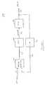
- FIG. 1is a block diagram of a phase-locked loop that may use VCOs consistent with embodiments of the present invention
- FIG. 2Ais a simplified schematic of a VCO that may incorporate embodiments of the present invention.
- FIG. 2Bis a plot of capacitance as a function of tuning voltage for a reverse-biased varactor diode that may be used in embodiments of the present invention
- FIG. 2Cis a side view of a varactor diode that may be used in an embodiment of the present invention.
- FIG. 3shows a conventional method of digitally adjusting the value of a capacitor
- FIG. 4is a schematic of a high-Q switching capacitor bank that may be used in embodiments of the present invention.
- FIG. 5is a schematic of another adjustable capacitance that may be used in embodiments of the present invention.
- FIG. 6is a schematic of a phase-locked loop in accordance with an embodiment of the present invention.
- FIG. 7is a flow chart of a method for tuning a VCO in accordance with an embodiment of the present invention.
- FIG. 8is a block diagram of an RF transceiver with a VCO in accordance with an embodiment of the present invention.
- FIG. 9shows a simplified block diagram for one example of an electronic system having optimized performance according to the present invention.
- FIG. 1is a block diagram of a phase-locked loop (PLL) 100 which may use VCOs consistent with embodiments of the present invention.
- PLLphase-locked loop
- This block diagram, as with all the included figures,is shown for illustrative purposes only, and does not limit either the possible applications of embodiments of the present invention, or the claims. Included are a phase detector 110 , low-pass filter (LPF) 120 , voltage controlled oscillator (VCO) 130 , and divider 140 .
- LPFlow-pass filter
- VCOvoltage controlled oscillator
- a reference clockis applied to the phase detector 110 on line 105 .
- the reference clockmay be generated by a crystal, or other periodic signal source.
- VCO 130provides an output signal Fout on line 135 .
- This signalas with the other signals, may be single-ended or differential. Often, Fout is differential, while Vtune and the reference clock are single-ended.
- the divider 140divides Fout's frequency, in this example by the value “m”.
- Phase detector 110compares the reference clock frequency to the frequency of the signal at the divider's output on line 145 , and outputs a signal on line 115 having an amplitude that is proportional to the differences in their frequencies.
- the signal on line 115is filtered by the low-pass filter 120 , and applied to the VCO 130 as Vtune on line 125 .
- the low-pass filter 120may be fully integrated on-chip, alternately some or all of the filter may be off-chip.
- the frequency of the output signal Fout from the VCO 130varies with changes in Vtune. If the frequency of the signal at the output of the divider 140 is higher than the reference clock, the signal at the output 115 of phase detector 110 , and thus Vtune, changes such that Fout's frequency decreases. Alternately, if the frequency of the signal at the output of the divider 140 is lower than the reference clock, the signal at the output 115 of phase detector 110 , and thus Vtune, changes such that Fout's frequency increases. In this way, the VCO output Fout on line 135 maintains a frequency that is a multiple “m” of the frequency of the reference clock applied on line 105 .
- a charge pumpmay be inserted between the phase detector 110 and low-pass filter 120 .
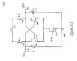
- FIG. 2Ais a simplified schematic of a VCO 200 which may incorporate embodiments of the present invention. Included are devices M 1 210 and M 2 220 , which form a differential pair connected in a positive feedback configuration, current source device M 3 230 , and an LC tank comprising inductors L 1 240 and L 2 250 and variable capacitors C 1 262 and C 2 264 .
- Lis the parallel combination of L 1 and L 2
- Cis the parallel combination of C 1 and C 2 . If the value of L 1 is equal to the value of L 2 , and the value of C 1 is equal to the value of C 2 , then L is one-half the value of L 1 , and C is twice the value of C 1 .
- L 1can be used for L
- C 1can be used for C, since the factors of 2 and one-half cancel.
- Calso includes stray capacitances of the inductor, drain and gate capacitances of the differential pair, parasitic capacitances of the interconnect lines, and other capacitances.
- the frequency of oscillation of this VCOmay be varied by changing the value of C.
- CMOScomplementary metal-oxide-semiconductor
- NMOScomplementary metal-oxide-semiconductor
- the devicesmay be HEMT, HBT, bipolar, JFET, p-channel MOS (PMOS), or other type device.
- the capacitorsmay be a series or parallel combination of capacitors. Specifically, the capacitors may be a parallel combination of multiple capacitors in series.
- the inductorsmay be on-chip spirals, bond wires, or traces, off-chip printed circuit board traces or inductors, a combination thereof, or other type inductor.
- FIG. 2Bshows capacitance as a function of tuning voltage for a varactor diode which may be used in embodiments of the present invention.
- the capacitance 296 of the varactor diodeis plotted on a graph having a Y-axis 294 of capacitance and an X axis 292 of reverse-bias voltage.
- the capacitanceis at a maximum value, and the change in capacitance per change in voltage (the first derivative of the capacitance) is also at a maximum. Both the capacitance and the change in capacitance per change in voltage decrease with increasing voltage. It will be appreciated by one skilled in the art that other diodes and voltage dependent capacitances may have other characteristics, and may also be used in embodiments of the present invention.
- FIG. 2Cis a side view of a junction varactor or varactor diode that may be used in an embodiment of the present invention.
- a p-well 284is diffused or implanted above a p-substrate 285 ; alternately the p-substrate itself may be used.
- an n-source/drain region 282or other suitable n-type region, is diffused or implanted.
- the n-source/drain to p-well interfacehas an associated capacitance 286 .
- This n-source/drain to p-well diodehas a capacitance that decreases with increasing reverse bias voltage—that is as the voltage of region 282 increases relative to the voltage of region 284 .
- variable capacitancesmay be used.
- a psource/drain to n-well diode or other p-n junctionmay be used.
- a MOS varactormay be used.
- a MOS varactormay be formed from an area or trace of polysilicon or metal over a n-well, p-well, or other region, where the polysilicon or metal is isolated by gate, field, “thin,” or other oxide.
- other insulating materialmay be used, and other materials than metal or polysilicon may be used.
- the variable capacitancemay be on-chip or off-chip, or partly on-chip and partly off-chip.
- FIG. 3shows a conventional method of digitally adjusting the capacitances in a VCO. Included are switch devices M 1 310 , M 2 320 , and M 3 330 , and capacitors C 1 340 , C 2 350 , and C 3 360 . Control voltages V 1 , V 2 , and V 3 are applied to devices M 1 310 , M 2 320 , and M 3 330 . If a control voltage is high, its corresponding device is on, and its corresponding capacitor is connected to the VCO tank. If a control voltage is low, its corresponding capacitance is disconnected from the VCO tank, and does not contribute to the VCO frequency. In this way, as the control voltages are switched, the capacitance at the tank circuit is varied, and the VCO is changed or tuned in frequency.
- K vcoThe K vco of an oscillator is defined as the change in frequency of the oscillator for a change in control voltage.
- a large K vcowould enable the VCO to tune over a wide range of frequency, and would reduce design concerns about capacitor and inductor tolerances, temperature and supply variations, and the like.
- the K vcois low, the immunity to noise on the control line is maximized. This means that the frequency of the VCO does not change excessively in the presence of noise or signal coupling on the control line. This is of particular concern since in most designs the control line is a single ended signal.
- a low K vcosuch that noise on the control line has a reduced effect on the VCO frequency, is at odds with having a broad tuning range, which requires a higher K vco .
- VCOvoltage-to-envelope-to-envelope-to-envelope-to-envelope-to-envelope-to-envelope-to-envelope-to-envelope-to-envelope-to-envelope-to-envelope-to-envelope-to-envelope-to-envelope-to-envelope-to-envelope-to-envelope-to-envelope-producing a signal.
- wireless transceiversoften need to be compliant with multiple standards, each operating over a different frequency range. Some standards require the VCO frequency to change periodically, such as in a frequency-hopping or spread-spectrum system.
- the variable capacitances shown below in FIGS. 4 and 5may be used to compensate for these process variations and to select between various transmission and reception bands.
- VCOvoltage-locked loops
- Vtuneon line 125 from the low-pass filter 120 in FIG. 1, or other sources.
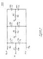
- FIG. 4is a schematic of a high-Q switching capacitor bank 400 , which may be used in embodiments of the present invention. Included are series of capacitors C 1 410 and C 2 420 , C 3 430 and C 4 440 , and C 5 450 and C 6 460 . Resistors R 1 470 , R 2 475 , and R 3 480 couple to the common node of the series of capacitors, and are driven by control voltages V 1 , V 2 , and V 3 . In a specific embodiment, these voltages are digital, in other embodiments they may be analog or digital. One skilled in the art appreciates that other numbers of capacitors and resistors may be used, three are shown here for exemplary purposes only.
- This circuitappears as a capacitance between nodes 485 and 490 .
- Node 490is shown as VSS.
- node 490can be VDD, or other appropriate a supply, control, bias, or circuit voltage.
- a high-Q switching capacitor bankmay replace all or part of the variable capacitance C 1 262 between nodes 270 and 290 , while another replaces all or part of C 2 264 between nodes 280 and 290 .
- capacitors C 2 420 , C 4 440 , and C 6 460are reverse-biased varactor diodes, or junction varactors. Alternately, capacitors C 2 420 , C 4 440 , and C 6 460 may be MOS varactors, or other variable capacitors.
- the control voltages V 1 , V 2 , and V 3are applied through resistors R 1 470 , R 2 475 , and R 3 480 to capacitors C 2 420 , C 4 440 , and C 6 460 .
- the average value of the voltage seen by capacitors C 2 420 , C 4 440 , and C 6 460is equal to the control voltages V 1 , V 2 , and V 3 .
- the control voltages V 1 , V 2 , and V 3determine the capacitance values of C 2 420 , C 4 440 , and C 6 460 .
- the resulting capacitancesare AC coupled through capacitors C 1 410 , C 3 430 , and C 5 450 to the VCO inductors, thus forming a tank circuit.
- the capacitors C 1 410 , C 3 430 , and C 5 450may be thin oxide, metal to metal, MOS, or other type of capacitor.
- the capacitorsmay use gate or other oxide, or other layer as insulating material. In a specific embodiment, these capacitors are designed to have a low voltage coefficient, that is their values do not vary strongly with changes in tune, supply, or control voltage.
- These capacitorsmay alternately be varactor capacitances, such as junction or MOS varactors, or other type of variable capacitors.
- the resistorsmay be resistors, parallel or series combinations of resistors, or properly biased active devices.
- the resistorsmay be formed from polysilicon, base or other diffusion or implant, or other resistive structure. For example, a resistor implant may be used.
- the AC pathis through the series capacitors between Fout line 485 and VSS line 490 . Accordingly, there are no resistors and the AC path, meaning the circuit has a high Q and improved phase noise, and is thus referred to as a high-Q switching capacitor bank. Moreover, the control voltage is DC blocked by the coupling capacitor. This means that the tank and varactor are isolated from each other. Because of this, both the output of the VCO and the tuning or control voltages can vary over the entire supply range, without forward biasing the varactor diodes.
- C 2 420 , C 4 440 , and C 6 460are MOS or junction varactors, while C 1 410 , C 3 430 , and C 5 450 are “fixed,” or low voltage sensitive, capacitors.
- the varactorsmay be junction varactors, such as a n-source-drain region in an p-well, a p-source drain region in an n-well or other appropriate structure, as discussed above. If a psource drain region is used, the diode may be coupled to VDD instead of VSS or ground as indicated in FIG. 4 .
- Other variable capacitorsmay be used instead of varactor diode capacitors.
- theybe MOS varactors, such as a polysilicon or metal trace isolated by gate or other oxide from an n-well, p-well, or other region.
- FIG. 5is a schematic 500 of a variable capacitance consistent with an embodiment of the present invention. Included are capacitors C 1 510 and C 2 520 , and isolation resistor R 1 530 . Capacitors C 1 510 and C 2 520 form a series of capacitors, with R 1 530 connected to the common point. In this embodiment, two control voltages are provided, specifically Vcont 1 on line 540 , which drives R 1 530 , and Vcont 2 on line 560 , which drives C 2 520 .
- This circuitappears as a capacitance between nodes 550 and 560 .
- a networkmay replace all or part of the variable capacitance C 1 262 , while another replaces all or part of C 2 264 .
- the capacitors C 1 262 and C 2 264connect to Vcont 2 rather than VSS as shown in FIG. 2 A.
- the circuits of FIGS. 4 and 5combine to form part of the capacitors C 1 262 and C 2 264 in FIG. 2 .
- capacitors C 1 510 and C 2 520are reverse-biased diodes or junction varactors. Alternately, they may be MOS capacitors.
- the capacitors C 1 510 and C 2 520 , and the resistor R 1 530may be constructed similar to capacitors C 1 410 or C 2 420 , and resistor R 1 470 in FIG. 4 .
- Vcont 2may be an analog control voltage from a phase-locked loop, such as the control voltage Vtune on line 125 in FIG. 1, while Vcont 1 may be a K vco control signal. Alternately, these functions may be reversed.
- the K vco control signalmay be continuous or digital.
- K vco of an oscillatoris the change in a VCO's oscillation frequency per change in control voltage.
- K vcois reduced by the presence of C 1 410 , C 3 430 , C 5 450 in FIG. 4, and C 1 510 in FIG. 5 .
- C 2 520varies as a function of Vcont 2 at a certain rate.
- the capacitance seen by the VCOis the series combination of C 1 510 and C 2 520 , the capacitance seen by the VCO varies as a function of voltage at a lower rate than does C 2 520 alone.
- the value of C 1 510may be adjusted by changing Vcont 1 such that the resulting K vco is no larger than required to tune the VCO over a desired range.
- a larger value of C 1 510results in more of the capacitance C 2 520 being coupled to the tank, leading to a higher K vco , while smaller valued C 1 510 passes less of the capacitance of C 2 520 , resulting in a lower K vco .
- Properly adjusting the value of C 1 510allows for maximum immunity to noise on the control line while still allowing the VCO to be tuned properly.
- the VCO of FIG. 2Amay incorporate the circuit of FIG. 5 as each of the variable capacitors C 1 262 and C 2 254 .
- Fout line 550 of FIG. 5connects to nodes 270 and 280 in FIG. 2A, and the capacitors connect to Vcont 2 rather than VSS.
- the voltage Fout on line 550has an average value of VDD, thus the average voltage across C 1 510 is VDD less the control voltage Vcont 1 on line 540 .
- the control voltage Vcont 1may be used to adjust the value of C 1 , and thus the K vco .
- the voltage across C 2 520is the voltage Veont 1 less the control voltage Vcont 2 on line 560 .
- the control voltage Vcont 2may be used to adjust the value of C 2 520 , and thus the frequency of oscillation of the VCO.
- FIG. 6is a schematic of a phase-locked loop 600 consistent with an embodiment of the present invention. Included are VCO pair M 1 610 and M 2 620 configured as a cross-coupled differential pair, current source M 3 630 , inductors L 1 632 and L 2 634 , and several tunable capacitance networks. Also included is a phase detector 640 , low-pass filter 670 , buffer 660 , and divider 650 . A control logic block 680 is also included, which outputs control logic signals V 1 through VN. These control signals are applied to resistors R 1 636 and R 2 638 , N- 2 pairs of intervening resistors not shown for simplicity, and R 3 652 and R 4 654 .
- control logic signalsmay be high or low, thus altering the value of effective capacitance contributed by capacitors C 1 642 , C 2 664 , C 3 646 , and C 4 648 , N- 2 pairs of series capacitors not shown for simplicity, and C 5 662 , C 6 664 , C 7 668 , and C 8 672 .
- the control logic signalscan be used for compensating for process tolerances, for band selection, and frequency hopping.
- a reference clockis applied to the phase detector 640 on line 645 .
- the reference clockmay be generated by a crystal, or other periodic signal source.
- the buffer 650isolates the VCO from the divider 650 .
- the divider 650divides the output frequency of the VCO, in this example by the value “m”.
- Phase detector 640compares the reference clock frequency to the frequency of the signal at the divider's output on line 145 , and outputs a signal having an amplitude that is proportional to the differences in their frequencies. That signal is filtered by the low-pass filter 670 resulting in Vcont on line 657 , which is applied to the isolation resistors R 5 656 and R 6 658 .
- the frequency of the VCO output signalvaries with changes in the Vcont signal on line 657 . If the frequency of the signal at the output of the divider 650 is higher than the reference clock, the signal at the output of phase detector 640 , and thus Vcont, changes such that the VCO's frequency decreases. Alternately, if the frequency of the signal at the output of the divider 650 is lower than the reference clock, the signal at the output of phase detector 640 , and thus Vcont, changes such that the VCO's frequency increases. In this way, the VCO output maintains a frequency that is a multiple “m” of the frequency of the reference clock applied on line 645 .
- a charge pumpmay be inserted between the phase detector 640 and low-pass filter 670 .
- the voltage V 1 on line 637may be VSS, VDD, or other control, bias, or circuit voltage.
- C 1 642 , C 5 662 , C 9 674 , C 4 648 , C 8 672 , and C 12 682are reversed-biased diodes or junction varactors, whose junction capacitances are determined by V 1 , VN, and Vcont. Again, these may alternately be MOS varactors.
- These variable capacitancesare AC coupled through C 2 644 , C 6 664 , C 10 676 , C 3 646 , C 7 668 , and C 11 678 to the inductors and nodes 612 and 614 .
- the values of the resulting capacitances, the inductors L 1 632 and L 2 634 , and the stray and parasitic capacitances and inductancesdetermine the frequency of oscillation of the VCO.
- the capacitors, resistors, and other componentsmay be the same or similar structures as those in FIGS. 4, 5 , and the other figures.
- FIG. 7is a flow chart of a method for tuning a VCO consistent with an embodiment of the present invention.
- the frequency of a VCOis measured.
- control logic signalsare generated based on a comparison of the measured frequency of the VCO and the desired frequency of the VCO.
- the control logic signalsare applied to a first plurality of resistors, where each resistor is coupled to the midpoint of a series of two capacitors, each of the series being coupled between a VCO node and a first node.
- This first nodemay be a control signal line, or any reference signal line such as supply, ground, or other bias point.
- a control voltageis applied to at least one resistor.
- This resistoris coupled to a midpoint of a series of two capacitors, each series being coupled between the node of the VCO and a second node.
- the second nodemay be connected to the first node, and the second node may be a control signal line, or any reference signal line such as supply, ground, or other bias point.
- FIG. 8is a block diagram of an RF transceiver 800 with a VCO 812 in accordance with an embodiment of the present invention. This block diagram is shown for illustrative purposes only, and does not limit either the possible applications of embodiments of the present invention, or the claims.
- An antenna switch 802operates to connect the antenna either to the receiver or the transmitter circuitry of transceiver 800 .
- the receive channelincludes a filter 804 that receives the signal from the antenna and operates to reject unwanted signals such as noise from adjacent channels.
- a low noise amplifier 806amplifies the signal at the output of filter 804 , and supplies it to in-phase (I) and quadrature-phase (Q) down-conversion mixers 808 and 810 , respectively.
- a voltage controlled oscillator 812generates a pair of local oscillating signals that are 90 degrees out-of-phase with respect to each other.
- the local oscillating signalsare respectively supplied to the I and Q mixers.
- DC offset reduction circuits 814 and 816are coupled around mixers 808 and 810 .
- An example of a preferred implementation of such an offset reduction circuitcan be found in commonly-assigned patent application Ser. No. 09/768,841, filed Jan. 23, 2001, attorney docket number 20798-001100US, which is incorporated by reference.
- the I and Q signalsare respectively filtered by low-pass filters (LPFs) 818 and 820 , and the filtered signals are applied to automatic gain control (AGC) circuits 822 and 824 .
- LPFslow-pass filters
- AGCautomatic gain control
- LPFs 818 and 820are described in greater detail in commonly-assigned patent application Ser. No. 09/612,116, titled “Active Circuit having LC Trap Functionality,” which is hereby incorporated by reference.
- the baseband signal processingis performed by block 826 that receives outputs of AGCs 822 and 824 and converts the analog signals to digital signals before processing them using, for example, orthogonal frequency division multiplexing (OFDM).
- block 826also provides media access control (MAC) functionality.
- the gain adjustment control signals 828 and 830are provided by block 826 . Control signal 828 adjusts the gain of AGCs 822 and 824 . Control signal 830 adjusts the gain of LNA 806 , DC offset reduction circuits 814 and 816 , and, in some embodiments, mixers 808 and 810 .
- the transmit channelincludes low-pass filters (LPFs) 832 and 834 that receive the I and Q signals and supply them to I and Q up-conversion mixers 836 and 838 .
- LPFslow-pass filters
- the up-converter mixers 836 and 838each receive one of the VCO output signals which are in quadrature.
- Mixers 836 and 838combine to form the image reject mixer discussed above with respect to FIG. 1 .
- the outputs of the two up-conversion mixersare combined and applied to a differential to single-ended converter 840 .
- An example of a preferred implementation of such an single-ended convertercan be found in commonly-assigned patent application Ser. No. 09/784,735, filed Feb.
- this block diagramimplements a 5 GHz RF transceiver according to the IEEE 802.11a standard.
- the differential to single-ended technique as embodied in the transceiver of FIG. 8allows for implementation of various electronic systems that are capable of wireless RF communication with optimized performance.
- Such electronic systemsinclude desktop and laptop personal computers, mobile telephone, television and internet devices, home gateways and media servers, portable digital music devices, data pipes and the like.
- FIG. 9shows a simplified block diagram for one example of an electronic system having optimized performance according to the present invention.
- a desktop personal computer 900is used for illustrative purposes.
- System 900includes a central processing unit (CPU) 902 , memory 904 , input/output (I/O) devices 906 and transceiver 908 all coupled to a common personal computer interface (PCI) bus 910 .
- CPUcentral processing unit
- memory 904volatile and non-volatile memory
- I/Oinput/output
- transceiver 908all coupled to a common personal computer interface (PCI) bus 910 .
- PCIpersonal computer interface
- Transceiver 908may be incorporated into and couple to PCI bus 910 via I/O devices block 906 .
- Transceiver 908is of the type described above in connection with FIG. 8 .
- Via PCI bus 910transceiver 908 allows system 900 to wirelessly communicate with other RF wireless devices.
Landscapes
- Inductance-Capacitance Distribution Constants And Capacitance-Resistance Oscillators (AREA)
Abstract
Description

Claims (25)
Priority Applications (1)
| Application Number | Priority Date | Filing Date | Title |
|---|---|---|---|
| US10/057,707US6778022B1 (en) | 2001-05-17 | 2002-01-24 | VCO with high-Q switching capacitor bank |
Applications Claiming Priority (2)
| Application Number | Priority Date | Filing Date | Title |
|---|---|---|---|
| US29225701P | 2001-05-17 | 2001-05-17 | |
| US10/057,707US6778022B1 (en) | 2001-05-17 | 2002-01-24 | VCO with high-Q switching capacitor bank |
Publications (1)
| Publication Number | Publication Date |
|---|---|
| US6778022B1true US6778022B1 (en) | 2004-08-17 |
Family
ID=32852880
Family Applications (1)
| Application Number | Title | Priority Date | Filing Date |
|---|---|---|---|
| US10/057,707Expired - LifetimeUS6778022B1 (en) | 2001-05-17 | 2002-01-24 | VCO with high-Q switching capacitor bank |
Country Status (1)
| Country | Link |
|---|---|
| US (1) | US6778022B1 (en) |
Cited By (33)
| Publication number | Priority date | Publication date | Assignee | Title |
|---|---|---|---|---|
| US20030132455A1 (en)* | 2001-10-16 | 2003-07-17 | Kimitake Utsunomiya | Methods and apparatus for implementing a receiver on a monolithic integrated circuit |
| US20030223017A1 (en)* | 2002-05-28 | 2003-12-04 | Kimitake Utsunomiya | Quadratic nyquist slope filter |
| US20050110528A1 (en)* | 2003-11-25 | 2005-05-26 | International Business Machines Corporation | Voltage controlled oscillator (vco) with amplitude control |
| US20050143039A1 (en)* | 2002-05-29 | 2005-06-30 | Takatsugu Kamata | Image rejection quadratic filter |
| US20050164465A1 (en)* | 2003-09-24 | 2005-07-28 | Intel Corporation | Vertical capacitor apparatus, systems, and methods |
| US20050190013A1 (en)* | 2002-06-05 | 2005-09-01 | Kimitake Utsunomiya | Frequency discrete LC filter bank |
| US20050264376A1 (en)* | 2003-07-18 | 2005-12-01 | Takatsugu Kamata | Methods and apparatus for an improved discrete LC filter |
| US7023282B1 (en) | 2004-05-11 | 2006-04-04 | Rf Micro Devices, Inc. | Coarse tuning for fractional-N synthesizers having reduced period comparison error |
| US20060097811A1 (en)* | 2004-11-09 | 2006-05-11 | Takahiro Nakamura | Variable inductor, and oscillator and communication system using the same |
| US7064591B1 (en) | 2004-05-11 | 2006-06-20 | Rf Micro Devices, Inc. | Coarse tuning for fractional-N synthesizers |
| US20060139138A1 (en)* | 2004-10-19 | 2006-06-29 | Daisuke Watanabe | Inductance variable device |
| US20060214723A1 (en)* | 2005-03-11 | 2006-09-28 | Takatsugu Kamata | MOSFET temperature compensation current source |
| US20060217095A1 (en)* | 2005-03-11 | 2006-09-28 | Takatsuga Kamata | Wideband tuning circuit |
| US7151363B1 (en) | 2004-06-08 | 2006-12-19 | Rf Micro Devices, Inc. | High PSRR, fast settle time voltage regulator |
| US20070132522A1 (en)* | 2005-12-08 | 2007-06-14 | Lee Ja Y | Multi-band LC resonance voltage-controlled oscillator with adjustable negative resistance cell |
| DE102006023353A1 (en)* | 2006-05-17 | 2007-11-22 | Atmel Duisburg Gmbh | Integrated resonant circuit |
| US20070268007A1 (en)* | 2006-05-17 | 2007-11-22 | Samir El Rai | Integrated tunable resonance circuit |
| US7333155B2 (en) | 2002-06-05 | 2008-02-19 | Rfstream Corporation | Quadratic video demodulation with baseband nyquist filter |
| US20080174388A1 (en)* | 2006-09-27 | 2008-07-24 | Thales | Compact power-agile filter, particularly for radiocommunication system amplification module |
| US7446631B2 (en) | 2005-03-11 | 2008-11-04 | Rf Stream Corporation | Radio frequency inductive-capacitive filter circuit topology |
| US7479839B1 (en) | 2008-03-31 | 2009-01-20 | International Business Machines Corporation | Varactor bank switching based on negative control voltage generation |
| US20090195336A1 (en)* | 2008-02-05 | 2009-08-06 | Cho-Chun Huang | Tunable voltage-controlled oscillator |
| US20090206939A1 (en)* | 2007-07-20 | 2009-08-20 | Christian Grewing | VCO Pre-Compensation |
| US20090215391A1 (en)* | 2008-02-01 | 2009-08-27 | Korea Advanced Institute Of Science And Technology | Apparatus and method for compensating inductance in inductive coupling communications |
| US20090243743A1 (en)* | 2008-03-31 | 2009-10-01 | International Business Machines Corporation | Varactor bank switching based on anti-parallel branch configuration |
| US20110204969A1 (en)* | 2010-02-19 | 2011-08-25 | Taiwan Semiconductor Manufacturing Company, Ltd. | Gated-varactors |
| US8928418B2 (en) | 2013-02-13 | 2015-01-06 | International Business Machines Corporation | Compensating for process variation in integrated circuit fabrication |
| US9602051B1 (en) | 2016-02-09 | 2017-03-21 | Cognitive Systems Corp. | Transforming voltage in a voltage controlled oscillator for wireless sensor devices |
| US9673755B1 (en) | 2016-02-09 | 2017-06-06 | Cognitive Systems Corp. | Controlling a switched capacitor bank in a voltage controlled oscillator for wireless sensor devices |
| US20170214409A1 (en)* | 2016-01-22 | 2017-07-27 | Kabushiki Kaisha Toshiba | Oscillator, radio communication device, and radio communication method |
| TWI620412B (en)* | 2012-12-27 | 2018-04-01 | 瑞薩電子股份有限公司 | Semiconductor device and method for adjusting filter circuit |
| US10461696B2 (en) | 2017-10-23 | 2019-10-29 | Analog Devices, Inc. | Switched capacitor banks |
| US10469029B2 (en) | 2017-10-23 | 2019-11-05 | Analog Devices, Inc. | Inductor current distribution |
Citations (13)
| Publication number | Priority date | Publication date | Assignee | Title |
|---|---|---|---|---|
| US3784917A (en)* | 1972-12-15 | 1974-01-08 | Philco Ford Corp | Constant lock-in range automatic frequency control |
| US4612585A (en) | 1982-09-10 | 1986-09-16 | Hitachi, Ltd. | Chrominance signal recording and reproducing apparatus |
| US4673892A (en)* | 1985-05-13 | 1987-06-16 | Nec Corporation | Phase locked loop frequency synthesizer with battery saving circuit |
| US4766497A (en) | 1987-05-06 | 1988-08-23 | Zenith Electronics Corporation | IF circuit with reduced sound attenuation for cable signals |
| JPH01208902A (en)* | 1988-02-16 | 1989-08-22 | Matsushita Electric Ind Co Ltd | voltage controlled oscillator |
| US5635892A (en) | 1994-12-06 | 1997-06-03 | Lucent Technologies Inc. | High Q integrated inductor |
| US5736749A (en) | 1996-11-19 | 1998-04-07 | Lucent Technologies Inc. | Integrated circuit device with inductor incorporated therein |
| US5745838A (en) | 1997-03-14 | 1998-04-28 | Tresness Irrevocable Patent Trust | Return path filter |
| US6008102A (en) | 1998-04-09 | 1999-12-28 | Motorola, Inc. | Method of forming a three-dimensional integrated inductor |
| US6031432A (en) | 1997-02-28 | 2000-02-29 | Schreuders; Ronald C. | Balancing apparatus for signal transmissions |
| US6233441B1 (en)* | 1998-05-29 | 2001-05-15 | Silicon Laboratories, Inc. | Method and apparatus for generating a discretely variable capacitance for synthesizing high-frequency signals for wireless communications |
| US6239665B1 (en)* | 1999-11-02 | 2001-05-29 | International Business Machines Corporation | Method and apparatus for switching in metal insulator metal capacitors and fet tuning capacitors for low noise oscillators |
| US6542043B1 (en)* | 2001-10-16 | 2003-04-01 | Broadcom Corporation | All PMOS fully differential voltage controlled oscillator |
- 2002
- 2002-01-24USUS10/057,707patent/US6778022B1/ennot_activeExpired - Lifetime
Patent Citations (13)
| Publication number | Priority date | Publication date | Assignee | Title |
|---|---|---|---|---|
| US3784917A (en)* | 1972-12-15 | 1974-01-08 | Philco Ford Corp | Constant lock-in range automatic frequency control |
| US4612585A (en) | 1982-09-10 | 1986-09-16 | Hitachi, Ltd. | Chrominance signal recording and reproducing apparatus |
| US4673892A (en)* | 1985-05-13 | 1987-06-16 | Nec Corporation | Phase locked loop frequency synthesizer with battery saving circuit |
| US4766497A (en) | 1987-05-06 | 1988-08-23 | Zenith Electronics Corporation | IF circuit with reduced sound attenuation for cable signals |
| JPH01208902A (en)* | 1988-02-16 | 1989-08-22 | Matsushita Electric Ind Co Ltd | voltage controlled oscillator |
| US5635892A (en) | 1994-12-06 | 1997-06-03 | Lucent Technologies Inc. | High Q integrated inductor |
| US5736749A (en) | 1996-11-19 | 1998-04-07 | Lucent Technologies Inc. | Integrated circuit device with inductor incorporated therein |
| US6031432A (en) | 1997-02-28 | 2000-02-29 | Schreuders; Ronald C. | Balancing apparatus for signal transmissions |
| US5745838A (en) | 1997-03-14 | 1998-04-28 | Tresness Irrevocable Patent Trust | Return path filter |
| US6008102A (en) | 1998-04-09 | 1999-12-28 | Motorola, Inc. | Method of forming a three-dimensional integrated inductor |
| US6233441B1 (en)* | 1998-05-29 | 2001-05-15 | Silicon Laboratories, Inc. | Method and apparatus for generating a discretely variable capacitance for synthesizing high-frequency signals for wireless communications |
| US6239665B1 (en)* | 1999-11-02 | 2001-05-29 | International Business Machines Corporation | Method and apparatus for switching in metal insulator metal capacitors and fet tuning capacitors for low noise oscillators |
| US6542043B1 (en)* | 2001-10-16 | 2003-04-01 | Broadcom Corporation | All PMOS fully differential voltage controlled oscillator |
Non-Patent Citations (10)
| Title |
|---|
| Bautista et al., "A High IIP2 Downconversion Mixer Using Dynamic Matching", IEEE Journal of Solid-State Circuits, vol. 35, No. 12, Dec. 2000, pp. 1934-1941. |
| Gibilisco "Handbook of Radio & Wireless Technology" McGraw-Hill 1999 p. 91.** |
| Lam et al., "A 2.6-GHz/5.2-GHz Frequency Synthesizer in 0.4-mum CMOS Technology", IEEE Journal of Solid-State Circuits, vol. 35, No. 5, May 2000, pp. 788-794. |
| Lam et al., "A 2.6-GHz/5.2-GHz Frequency Synthesizer in 0.4-μm CMOS Technology", IEEE Journal of Solid-State Circuits, vol. 35, No. 5, May 2000, pp. 788-794. |
| Liu et al., "5-GHz CMOS Radio Transceiver Front-End Chipset", IEEE Journal of Solid-State Circuits, vol. 35, No. 12, Dec. 2000, pp. 1927-1933. |
| Rategh et al., "A CMOS Frequency Synthesizer with an Injection-Locked Frequency Divider for a 5-GHz Wireless LAN Receiver", IEEE Journal of Solid-State Circuits, vol. 35, No. 5, May 2000, pp. 780-787. |
| Rogers et al. "The effect of varactor nonlinearity on the phase noise of completely integrated VCO's" IEEE Journal of Solid-State Circuits, No 35 Issue 9 Sep. 2000 pp 1360-1367.** |
| Samavati et al., "A 5-GHz CMOS Wireless LAN Receiver Front End", IEEE Journal of Solid-State Circuits, vol. 35, No. 5, May 2000, pp. 765-772. |
| Steyaert et al., "A 2-V CMOS Cellular Transceiver Front-End", IEEE Journal of Solid-State Circuits, vol. 35, No. 12, Dec. 2000, pp. 195-1907. |
| Wong et al., "A Wide Turning Range Gated Varactor", IEEE Journal of Solid-State Circuits, vol. 35, No. 5, May 2000, pp. 773-779. |
Cited By (61)
| Publication number | Priority date | Publication date | Assignee | Title |
|---|---|---|---|---|
| US20030132455A1 (en)* | 2001-10-16 | 2003-07-17 | Kimitake Utsunomiya | Methods and apparatus for implementing a receiver on a monolithic integrated circuit |
| US7327406B2 (en) | 2001-10-16 | 2008-02-05 | Rfstream Corporation | Methods and apparatus for implementing a receiver on a monolithic integrated circuit |
| US20030223017A1 (en)* | 2002-05-28 | 2003-12-04 | Kimitake Utsunomiya | Quadratic nyquist slope filter |
| US7199844B2 (en) | 2002-05-28 | 2007-04-03 | Rfstream Corporation | Quadratic nyquist slope filter |
| US20050143039A1 (en)* | 2002-05-29 | 2005-06-30 | Takatsugu Kamata | Image rejection quadratic filter |
| US7116961B2 (en) | 2002-05-29 | 2006-10-03 | Rfstream Corporation | Image rejection quadratic filter |
| US7333155B2 (en) | 2002-06-05 | 2008-02-19 | Rfstream Corporation | Quadratic video demodulation with baseband nyquist filter |
| US20050190013A1 (en)* | 2002-06-05 | 2005-09-01 | Kimitake Utsunomiya | Frequency discrete LC filter bank |
| US7102465B2 (en) | 2002-06-05 | 2006-09-05 | Rfstream Corporation | Frequency discrete LC filter bank |
| US7183880B2 (en) | 2003-07-18 | 2007-02-27 | Rfstream Corporation | Discrete inductor bank and LC filter |
| US7088202B2 (en)* | 2003-07-18 | 2006-08-08 | Rfstream Corporation | Methods and apparatus for an improved discrete LC filter |
| US20050264376A1 (en)* | 2003-07-18 | 2005-12-01 | Takatsugu Kamata | Methods and apparatus for an improved discrete LC filter |
| US20050164465A1 (en)* | 2003-09-24 | 2005-07-28 | Intel Corporation | Vertical capacitor apparatus, systems, and methods |
| US7352557B2 (en)* | 2003-09-24 | 2008-04-01 | Intel Corporation | Vertical capacitor apparatus, systems, and methods |
| US6954088B2 (en)* | 2003-11-25 | 2005-10-11 | International Business Machines Corporation | Voltage controlled oscillator (VCO) with amplitude control |
| US20050110528A1 (en)* | 2003-11-25 | 2005-05-26 | International Business Machines Corporation | Voltage controlled oscillator (vco) with amplitude control |
| US7023282B1 (en) | 2004-05-11 | 2006-04-04 | Rf Micro Devices, Inc. | Coarse tuning for fractional-N synthesizers having reduced period comparison error |
| US7064591B1 (en) | 2004-05-11 | 2006-06-20 | Rf Micro Devices, Inc. | Coarse tuning for fractional-N synthesizers |
| US7274229B1 (en) | 2004-05-11 | 2007-09-25 | Rf Micro Devices, Inc. | Coarse tuning for fractional-N synthesizers |
| US7151363B1 (en) | 2004-06-08 | 2006-12-19 | Rf Micro Devices, Inc. | High PSRR, fast settle time voltage regulator |
| US7348871B2 (en) | 2004-10-19 | 2008-03-25 | Matsushita Electric Industrial Co., Ltd. | Inductance variable device |
| US20060139138A1 (en)* | 2004-10-19 | 2006-06-29 | Daisuke Watanabe | Inductance variable device |
| US20080055037A1 (en)* | 2004-10-19 | 2008-03-06 | Daisuke Watanabe | Inductance variable device |
| US20070176721A1 (en)* | 2004-10-19 | 2007-08-02 | Daisuke Watanabe | Inductance variable device |
| US7336147B2 (en)* | 2004-10-19 | 2008-02-26 | Matsushita Electric Industrial Co., Ltd. | Inductance variable device |
| US20110105053A1 (en)* | 2004-11-09 | 2011-05-05 | Renesas Electronics Corporation | Variable inductor, and oscillator and communication system using the same |
| US7902934B2 (en)* | 2004-11-09 | 2011-03-08 | Renesas Electronics Corporation | Variable inductor, and oscillator and communication system using the same |
| US20060097811A1 (en)* | 2004-11-09 | 2006-05-11 | Takahiro Nakamura | Variable inductor, and oscillator and communication system using the same |
| US8502614B2 (en) | 2004-11-09 | 2013-08-06 | Renesas Electronics Corporation | Variable inductor, and oscillator and communication system using the same |
| US7446631B2 (en) | 2005-03-11 | 2008-11-04 | Rf Stream Corporation | Radio frequency inductive-capacitive filter circuit topology |
| US20060217095A1 (en)* | 2005-03-11 | 2006-09-28 | Takatsuga Kamata | Wideband tuning circuit |
| US20060214723A1 (en)* | 2005-03-11 | 2006-09-28 | Takatsugu Kamata | MOSFET temperature compensation current source |
| US7358795B2 (en) | 2005-03-11 | 2008-04-15 | Rfstream Corporation | MOSFET temperature compensation current source |
| US7554416B2 (en) | 2005-12-08 | 2009-06-30 | Electronics And Telecommunications Research Institute | Multi-band LC resonance voltage-controlled oscillator with adjustable negative resistance cell |
| US20070132522A1 (en)* | 2005-12-08 | 2007-06-14 | Lee Ja Y | Multi-band LC resonance voltage-controlled oscillator with adjustable negative resistance cell |
| WO2007131576A1 (en)* | 2006-05-17 | 2007-11-22 | Atmel Duisburg Gmbh | Integrated, tunable oscillating circuit |
| DE102006023353A1 (en)* | 2006-05-17 | 2007-11-22 | Atmel Duisburg Gmbh | Integrated resonant circuit |
| US7633352B2 (en) | 2006-05-17 | 2009-12-15 | Atmel Duisburg Gmbh | Integrated tunable resonance circuit |
| US20070268007A1 (en)* | 2006-05-17 | 2007-11-22 | Samir El Rai | Integrated tunable resonance circuit |
| DE102006023352A1 (en)* | 2006-05-17 | 2007-11-22 | Atmel Duisburg Gmbh | Integrated tunable resonant circuit |
| US20080174388A1 (en)* | 2006-09-27 | 2008-07-24 | Thales | Compact power-agile filter, particularly for radiocommunication system amplification module |
| US7812690B2 (en)* | 2006-09-27 | 2010-10-12 | Thales | Compact power-agile filter, particularly for radiocommunication system amplification module |
| US8368479B2 (en) | 2007-07-20 | 2013-02-05 | Infineon Technologies Ag | VCO pre-compensation |
| US20090206939A1 (en)* | 2007-07-20 | 2009-08-20 | Christian Grewing | VCO Pre-Compensation |
| US20090215391A1 (en)* | 2008-02-01 | 2009-08-27 | Korea Advanced Institute Of Science And Technology | Apparatus and method for compensating inductance in inductive coupling communications |
| US8244187B2 (en)* | 2008-02-01 | 2012-08-14 | Korea Advanced Institute Of Science And Technology | Apparatus and method for compensating inductance in inductive coupling communications |
| US20090195336A1 (en)* | 2008-02-05 | 2009-08-06 | Cho-Chun Huang | Tunable voltage-controlled oscillator |
| US20090243743A1 (en)* | 2008-03-31 | 2009-10-01 | International Business Machines Corporation | Varactor bank switching based on anti-parallel branch configuration |
| US20090243702A1 (en)* | 2008-03-31 | 2009-10-01 | International Business Machines Corporation | Varactor bank switching based on negative control voltage generation |
| US7479839B1 (en) | 2008-03-31 | 2009-01-20 | International Business Machines Corporation | Varactor bank switching based on negative control voltage generation |
| US20110204969A1 (en)* | 2010-02-19 | 2011-08-25 | Taiwan Semiconductor Manufacturing Company, Ltd. | Gated-varactors |
| US8273616B2 (en)* | 2010-02-19 | 2012-09-25 | Taiwan Semiconductor Manufacturing Company, Ltd. | Gated-varactors |
| US8609479B2 (en) | 2010-02-19 | 2013-12-17 | Taiwan Semiconductor Manufacturing Company, Ltd. | Gated-varactors |
| TWI620412B (en)* | 2012-12-27 | 2018-04-01 | 瑞薩電子股份有限公司 | Semiconductor device and method for adjusting filter circuit |
| US8928418B2 (en) | 2013-02-13 | 2015-01-06 | International Business Machines Corporation | Compensating for process variation in integrated circuit fabrication |
| US20170214409A1 (en)* | 2016-01-22 | 2017-07-27 | Kabushiki Kaisha Toshiba | Oscillator, radio communication device, and radio communication method |
| US9866224B2 (en)* | 2016-01-22 | 2018-01-09 | Kabushiki Kaisha Toshiba | Oscillator, radio communication device, and radio communication method |
| US9602051B1 (en) | 2016-02-09 | 2017-03-21 | Cognitive Systems Corp. | Transforming voltage in a voltage controlled oscillator for wireless sensor devices |
| US9673755B1 (en) | 2016-02-09 | 2017-06-06 | Cognitive Systems Corp. | Controlling a switched capacitor bank in a voltage controlled oscillator for wireless sensor devices |
| US10461696B2 (en) | 2017-10-23 | 2019-10-29 | Analog Devices, Inc. | Switched capacitor banks |
| US10469029B2 (en) | 2017-10-23 | 2019-11-05 | Analog Devices, Inc. | Inductor current distribution |
Similar Documents
| Publication | Publication Date | Title |
|---|---|---|
| US6778022B1 (en) | VCO with high-Q switching capacitor bank | |
| US7209017B2 (en) | Symmetrical linear voltage controlled oscillator | |
| US6833769B2 (en) | Voltage controlled capacitive elements having a biasing network | |
| US7518458B2 (en) | Oscillator and data processing equipment using the same and voltage control oscillator and data processing equipment using voltage control oscillator | |
| JP5036966B2 (en) | LC oscillator with wide tuning range and low phase noise | |
| US9236872B2 (en) | Voltage-controlled oscillator, signal generation apparatus, and electronic device | |
| US8067995B2 (en) | Voltage controlled oscillator, and PLL circuit and wireless communication device each using the same | |
| US20030227341A1 (en) | Voltage-controlled oscillator and frequency synthesizer | |
| US7622967B2 (en) | Phase shifting circuit having a constant phase shift | |
| US20110215848A1 (en) | Frequency synthesizer | |
| EP1583221A1 (en) | PLL frequency synthesizer circuit and frequency tuning method thereof | |
| US20090108947A1 (en) | Voltage Controlled Oscillator | |
| EP2005592B1 (en) | Differing charge pump currents for integrated pll filter | |
| EP1589655B1 (en) | Wideband voltage controlled oscillator employing evanescent mode coupled-resonators | |
| US6236238B1 (en) | Output buffer with independently controllable current mirror legs | |
| US7015768B1 (en) | Low noise voltage-controlled oscillator | |
| US20050225398A1 (en) | Oscillating circuit having a noise reduction circuit | |
| KR102503742B1 (en) | Wideband Phase Locked Loops for Multi-Band Millimeter Wave 5G Communications | |
| US7098747B2 (en) | Precision tunable voltage controlled oscillation and applications thereof | |
| Ruffieux et al. | A 1.2 mW RDS receiver for portable applications | |
| US7082295B2 (en) | On-chip loop filter for use in a phase locked loop and other applications | |
| US7057466B2 (en) | Varactor-based ring oscillator | |
| CN1701512B (en) | VCO device | |
| US7205857B2 (en) | Oscillator with quadrature output in a cross-coupled configuration | |
| EP1619789B1 (en) | Low thermal drift, tunable frequency voltage controlled oscillator |
Legal Events
| Date | Code | Title | Description |
|---|---|---|---|
| AS | Assignment | Owner name:RESONEXT COMMUNICATIONS, INC., CALIFORNIA Free format text:ASSIGNMENT OF ASSIGNORS INTEREST;ASSIGNORS:ZHANG, PENGFEI;SOORAPANTH, CHET;REEL/FRAME:012545/0527;SIGNING DATES FROM 20020122 TO 20020123 | |
| AS | Assignment | Owner name:RF MICRO DEVICES, INC., NORTH CAROLINA Free format text:MERGER;ASSIGNOR:RESONEXT COMMUNICATIONS, INC.;REEL/FRAME:013957/0507 Effective date:20021219 | |
| STCF | Information on status: patent grant | Free format text:PATENTED CASE | |
| FEPP | Fee payment procedure | Free format text:PAT HOLDER NO LONGER CLAIMS SMALL ENTITY STATUS, ENTITY STATUS SET TO UNDISCOUNTED (ORIGINAL EVENT CODE: STOL); ENTITY STATUS OF PATENT OWNER: LARGE ENTITY | |
| FPAY | Fee payment | Year of fee payment:4 | |
| FPAY | Fee payment | Year of fee payment:8 | |
| AS | Assignment | Owner name:BANK OF AMERICA, N.A., AS ADMINISTRATIVE AGENT, TE Free format text:NOTICE OF GRANT OF SECURITY INTEREST IN PATENTS;ASSIGNOR:RF MICRO DEVICES, INC.;REEL/FRAME:030045/0831 Effective date:20130319 | |
| AS | Assignment | Owner name:RF MICRO DEVICES, INC., NORTH CAROLINA Free format text:TERMINATION AND RELEASE OF SECURITY INTEREST IN PATENTS (RECORDED 3/19/13 AT REEL/FRAME 030045/0831);ASSIGNOR:BANK OF AMERICA, N.A., AS ADMINISTRATIVE AGENT;REEL/FRAME:035334/0363 Effective date:20150326 | |
| REMI | Maintenance fee reminder mailed | ||
| FPAY | Fee payment | Year of fee payment:12 | |
| SULP | Surcharge for late payment | Year of fee payment:11 | |
| AS | Assignment | Owner name:QORVO US, INC., NORTH CAROLINA Free format text:MERGER;ASSIGNOR:RF MICRO DEVICES, INC.;REEL/FRAME:039196/0941 Effective date:20160330 |