US6777800B2 - Semiconductor die package including drain clip - Google Patents
Semiconductor die package including drain clipDownload PDFInfo
- Publication number
- US6777800B2 US6777800B2US10/262,170US26217002AUS6777800B2US 6777800 B2US6777800 B2US 6777800B2US 26217002 AUS26217002 AUS 26217002AUS 6777800 B2US6777800 B2US 6777800B2
- Authority
- US
- United States
- Prior art keywords
- drain
- semiconductor die
- region
- lead
- source
- Prior art date
- Legal status (The legal status is an assumption and is not a legal conclusion. Google has not performed a legal analysis and makes no representation as to the accuracy of the status listed.)
- Expired - Lifetime, expires
Links
- 239000004065semiconductorSubstances0.000titleclaimsabstractdescription120
- 239000012778molding materialSubstances0.000claimsabstractdescription56
- 229910000679solderInorganic materials0.000claimsdescription27
- 238000000034methodMethods0.000claimsdescription22
- 238000000465mouldingMethods0.000claimsdescription8
- RYGMFSIKBFXOCR-UHFFFAOYSA-NCopperChemical compound[Cu]RYGMFSIKBFXOCR-UHFFFAOYSA-N0.000claimsdescription6
- 229910052802copperInorganic materials0.000claimsdescription6
- 239000010949copperSubstances0.000claimsdescription6
- 238000005530etchingMethods0.000claimsdescription6
- 230000005496eutecticsEffects0.000description2
- 230000014509gene expressionEffects0.000description2
- 238000004519manufacturing processMethods0.000description2
- 238000013021overheatingMethods0.000description2
- 229910045601alloyInorganic materials0.000description1
- 239000000956alloySubstances0.000description1
- 238000005452bendingMethods0.000description1
- 150000001875compoundsChemical class0.000description1
- 238000011109contaminationMethods0.000description1
- 238000001816coolingMethods0.000description1
- 238000005260corrosionMethods0.000description1
- 230000007797corrosionEffects0.000description1
- 238000010586diagramMethods0.000description1
- 239000003989dielectric materialSubstances0.000description1
- 238000009792diffusion processMethods0.000description1
- 238000001312dry etchingMethods0.000description1
- 230000005669field effectEffects0.000description1
- 230000017525heat dissipationEffects0.000description1
- 238000010330laser markingMethods0.000description1
- 229910044991metal oxideInorganic materials0.000description1
- 150000004706metal oxidesChemical class0.000description1
- 238000012986modificationMethods0.000description1
- 230000004048modificationEffects0.000description1
- 238000004806packaging method and processMethods0.000description1
- 238000000206photolithographyMethods0.000description1
- 229920002120photoresistant polymerPolymers0.000description1
- 238000001039wet etchingMethods0.000description1
Images


Classifications
- H—ELECTRICITY
- H01—ELECTRIC ELEMENTS
- H01L—SEMICONDUCTOR DEVICES NOT COVERED BY CLASS H10
- H01L24/00—Arrangements for connecting or disconnecting semiconductor or solid-state bodies; Methods or apparatus related thereto
- H01L24/73—Means for bonding being of different types provided for in two or more of groups H01L24/10, H01L24/18, H01L24/26, H01L24/34, H01L24/42, H01L24/50, H01L24/63, H01L24/71
- H—ELECTRICITY
- H01—ELECTRIC ELEMENTS
- H01L—SEMICONDUCTOR DEVICES NOT COVERED BY CLASS H10
- H01L23/00—Details of semiconductor or other solid state devices
- H01L23/48—Arrangements for conducting electric current to or from the solid state body in operation, e.g. leads, terminal arrangements ; Selection of materials therefor
- H01L23/488—Arrangements for conducting electric current to or from the solid state body in operation, e.g. leads, terminal arrangements ; Selection of materials therefor consisting of soldered or bonded constructions
- H01L23/495—Lead-frames or other flat leads
- H01L23/49517—Additional leads
- H01L23/49524—Additional leads the additional leads being a tape carrier or flat leads
- H—ELECTRICITY
- H01—ELECTRIC ELEMENTS
- H01L—SEMICONDUCTOR DEVICES NOT COVERED BY CLASS H10
- H01L23/00—Details of semiconductor or other solid state devices
- H01L23/48—Arrangements for conducting electric current to or from the solid state body in operation, e.g. leads, terminal arrangements ; Selection of materials therefor
- H01L23/488—Arrangements for conducting electric current to or from the solid state body in operation, e.g. leads, terminal arrangements ; Selection of materials therefor consisting of soldered or bonded constructions
- H01L23/495—Lead-frames or other flat leads
- H01L23/49541—Geometry of the lead-frame
- H01L23/49562—Geometry of the lead-frame for individual devices of subclass H10D
- H—ELECTRICITY
- H01—ELECTRIC ELEMENTS
- H01L—SEMICONDUCTOR DEVICES NOT COVERED BY CLASS H10
- H01L24/00—Arrangements for connecting or disconnecting semiconductor or solid-state bodies; Methods or apparatus related thereto
- H01L24/01—Means for bonding being attached to, or being formed on, the surface to be connected, e.g. chip-to-package, die-attach, "first-level" interconnects; Manufacturing methods related thereto
- H01L24/34—Strap connectors, e.g. copper straps for grounding power devices; Manufacturing methods related thereto
- H01L24/36—Structure, shape, material or disposition of the strap connectors prior to the connecting process
- H01L24/37—Structure, shape, material or disposition of the strap connectors prior to the connecting process of an individual strap connector
- H—ELECTRICITY
- H01—ELECTRIC ELEMENTS
- H01L—SEMICONDUCTOR DEVICES NOT COVERED BY CLASS H10
- H01L24/00—Arrangements for connecting or disconnecting semiconductor or solid-state bodies; Methods or apparatus related thereto
- H01L24/01—Means for bonding being attached to, or being formed on, the surface to be connected, e.g. chip-to-package, die-attach, "first-level" interconnects; Manufacturing methods related thereto
- H01L24/34—Strap connectors, e.g. copper straps for grounding power devices; Manufacturing methods related thereto
- H01L24/39—Structure, shape, material or disposition of the strap connectors after the connecting process
- H01L24/40—Structure, shape, material or disposition of the strap connectors after the connecting process of an individual strap connector
- H—ELECTRICITY
- H01—ELECTRIC ELEMENTS
- H01L—SEMICONDUCTOR DEVICES NOT COVERED BY CLASS H10
- H01L24/00—Arrangements for connecting or disconnecting semiconductor or solid-state bodies; Methods or apparatus related thereto
- H01L24/80—Methods for connecting semiconductor or other solid state bodies using means for bonding being attached to, or being formed on, the surface to be connected
- H01L24/84—Methods for connecting semiconductor or other solid state bodies using means for bonding being attached to, or being formed on, the surface to be connected using a strap connector
- H—ELECTRICITY
- H01—ELECTRIC ELEMENTS
- H01L—SEMICONDUCTOR DEVICES NOT COVERED BY CLASS H10
- H01L2224/00—Indexing scheme for arrangements for connecting or disconnecting semiconductor or solid-state bodies and methods related thereto as covered by H01L24/00
- H01L2224/01—Means for bonding being attached to, or being formed on, the surface to be connected, e.g. chip-to-package, die-attach, "first-level" interconnects; Manufacturing methods related thereto
- H01L2224/10—Bump connectors; Manufacturing methods related thereto
- H01L2224/15—Structure, shape, material or disposition of the bump connectors after the connecting process
- H01L2224/16—Structure, shape, material or disposition of the bump connectors after the connecting process of an individual bump connector
- H01L2224/161—Disposition
- H01L2224/16151—Disposition the bump connector connecting between a semiconductor or solid-state body and an item not being a semiconductor or solid-state body, e.g. chip-to-substrate, chip-to-passive
- H01L2224/16221—Disposition the bump connector connecting between a semiconductor or solid-state body and an item not being a semiconductor or solid-state body, e.g. chip-to-substrate, chip-to-passive the body and the item being stacked
- H01L2224/16245—Disposition the bump connector connecting between a semiconductor or solid-state body and an item not being a semiconductor or solid-state body, e.g. chip-to-substrate, chip-to-passive the body and the item being stacked the item being metallic
- H—ELECTRICITY
- H01—ELECTRIC ELEMENTS
- H01L—SEMICONDUCTOR DEVICES NOT COVERED BY CLASS H10
- H01L2224/00—Indexing scheme for arrangements for connecting or disconnecting semiconductor or solid-state bodies and methods related thereto as covered by H01L24/00
- H01L2224/01—Means for bonding being attached to, or being formed on, the surface to be connected, e.g. chip-to-package, die-attach, "first-level" interconnects; Manufacturing methods related thereto
- H01L2224/34—Strap connectors, e.g. copper straps for grounding power devices; Manufacturing methods related thereto
- H01L2224/36—Structure, shape, material or disposition of the strap connectors prior to the connecting process
- H01L2224/37—Structure, shape, material or disposition of the strap connectors prior to the connecting process of an individual strap connector
- H01L2224/37001—Core members of the connector
- H01L2224/37099—Material
- H01L2224/371—Material with a principal constituent of the material being a metal or a metalloid, e.g. boron [B], silicon [Si], germanium [Ge], arsenic [As], antimony [Sb], tellurium [Te] and polonium [Po], and alloys thereof
- H01L2224/37138—Material with a principal constituent of the material being a metal or a metalloid, e.g. boron [B], silicon [Si], germanium [Ge], arsenic [As], antimony [Sb], tellurium [Te] and polonium [Po], and alloys thereof the principal constituent melting at a temperature of greater than or equal to 950°C and less than 1550°C
- H01L2224/37147—Copper [Cu] as principal constituent
- H—ELECTRICITY
- H01—ELECTRIC ELEMENTS
- H01L—SEMICONDUCTOR DEVICES NOT COVERED BY CLASS H10
- H01L2224/00—Indexing scheme for arrangements for connecting or disconnecting semiconductor or solid-state bodies and methods related thereto as covered by H01L24/00
- H01L2224/01—Means for bonding being attached to, or being formed on, the surface to be connected, e.g. chip-to-package, die-attach, "first-level" interconnects; Manufacturing methods related thereto
- H01L2224/34—Strap connectors, e.g. copper straps for grounding power devices; Manufacturing methods related thereto
- H01L2224/39—Structure, shape, material or disposition of the strap connectors after the connecting process
- H01L2224/40—Structure, shape, material or disposition of the strap connectors after the connecting process of an individual strap connector
- H01L2224/4005—Shape
- H01L2224/4009—Loop shape
- H01L2224/40095—Kinked
- H—ELECTRICITY
- H01—ELECTRIC ELEMENTS
- H01L—SEMICONDUCTOR DEVICES NOT COVERED BY CLASS H10
- H01L2224/00—Indexing scheme for arrangements for connecting or disconnecting semiconductor or solid-state bodies and methods related thereto as covered by H01L24/00
- H01L2224/01—Means for bonding being attached to, or being formed on, the surface to be connected, e.g. chip-to-package, die-attach, "first-level" interconnects; Manufacturing methods related thereto
- H01L2224/34—Strap connectors, e.g. copper straps for grounding power devices; Manufacturing methods related thereto
- H01L2224/39—Structure, shape, material or disposition of the strap connectors after the connecting process
- H01L2224/40—Structure, shape, material or disposition of the strap connectors after the connecting process of an individual strap connector
- H01L2224/401—Disposition
- H01L2224/40151—Connecting between a semiconductor or solid-state body and an item not being a semiconductor or solid-state body, e.g. chip-to-substrate, chip-to-passive
- H01L2224/40221—Connecting between a semiconductor or solid-state body and an item not being a semiconductor or solid-state body, e.g. chip-to-substrate, chip-to-passive the body and the item being stacked
- H01L2224/40245—Connecting between a semiconductor or solid-state body and an item not being a semiconductor or solid-state body, e.g. chip-to-substrate, chip-to-passive the body and the item being stacked the item being metallic
- H—ELECTRICITY
- H01—ELECTRIC ELEMENTS
- H01L—SEMICONDUCTOR DEVICES NOT COVERED BY CLASS H10
- H01L2224/00—Indexing scheme for arrangements for connecting or disconnecting semiconductor or solid-state bodies and methods related thereto as covered by H01L24/00
- H01L2224/73—Means for bonding being of different types provided for in two or more of groups H01L2224/10, H01L2224/18, H01L2224/26, H01L2224/34, H01L2224/42, H01L2224/50, H01L2224/63, H01L2224/71
- H01L2224/732—Location after the connecting process
- H01L2224/73251—Location after the connecting process on different surfaces
- H01L2224/73253—Bump and layer connectors
- H—ELECTRICITY
- H01—ELECTRIC ELEMENTS
- H01L—SEMICONDUCTOR DEVICES NOT COVERED BY CLASS H10
- H01L2224/00—Indexing scheme for arrangements for connecting or disconnecting semiconductor or solid-state bodies and methods related thereto as covered by H01L24/00
- H01L2224/73—Means for bonding being of different types provided for in two or more of groups H01L2224/10, H01L2224/18, H01L2224/26, H01L2224/34, H01L2224/42, H01L2224/50, H01L2224/63, H01L2224/71
- H01L2224/732—Location after the connecting process
- H01L2224/73251—Location after the connecting process on different surfaces
- H01L2224/73255—Bump and strap connectors
- H—ELECTRICITY
- H01—ELECTRIC ELEMENTS
- H01L—SEMICONDUCTOR DEVICES NOT COVERED BY CLASS H10
- H01L2224/00—Indexing scheme for arrangements for connecting or disconnecting semiconductor or solid-state bodies and methods related thereto as covered by H01L24/00
- H01L2224/80—Methods for connecting semiconductor or other solid state bodies using means for bonding being attached to, or being formed on, the surface to be connected
- H01L2224/83—Methods for connecting semiconductor or other solid state bodies using means for bonding being attached to, or being formed on, the surface to be connected using a layer connector
- H01L2224/838—Bonding techniques
- H01L2224/83801—Soldering or alloying
- H—ELECTRICITY
- H01—ELECTRIC ELEMENTS
- H01L—SEMICONDUCTOR DEVICES NOT COVERED BY CLASS H10
- H01L2224/00—Indexing scheme for arrangements for connecting or disconnecting semiconductor or solid-state bodies and methods related thereto as covered by H01L24/00
- H01L2224/80—Methods for connecting semiconductor or other solid state bodies using means for bonding being attached to, or being formed on, the surface to be connected
- H01L2224/84—Methods for connecting semiconductor or other solid state bodies using means for bonding being attached to, or being formed on, the surface to be connected using a strap connector
- H01L2224/8434—Bonding interfaces of the connector
- H01L2224/84345—Shape, e.g. interlocking features
- H—ELECTRICITY
- H01—ELECTRIC ELEMENTS
- H01L—SEMICONDUCTOR DEVICES NOT COVERED BY CLASS H10
- H01L2224/00—Indexing scheme for arrangements for connecting or disconnecting semiconductor or solid-state bodies and methods related thereto as covered by H01L24/00
- H01L2224/80—Methods for connecting semiconductor or other solid state bodies using means for bonding being attached to, or being formed on, the surface to be connected
- H01L2224/84—Methods for connecting semiconductor or other solid state bodies using means for bonding being attached to, or being formed on, the surface to be connected using a strap connector
- H01L2224/8438—Bonding interfaces outside the semiconductor or solid-state body
- H01L2224/84385—Shape, e.g. interlocking features
- H—ELECTRICITY
- H01—ELECTRIC ELEMENTS
- H01L—SEMICONDUCTOR DEVICES NOT COVERED BY CLASS H10
- H01L2224/00—Indexing scheme for arrangements for connecting or disconnecting semiconductor or solid-state bodies and methods related thereto as covered by H01L24/00
- H01L2224/80—Methods for connecting semiconductor or other solid state bodies using means for bonding being attached to, or being formed on, the surface to be connected
- H01L2224/84—Methods for connecting semiconductor or other solid state bodies using means for bonding being attached to, or being formed on, the surface to be connected using a strap connector
- H01L2224/848—Bonding techniques
- H01L2224/84801—Soldering or alloying
- H—ELECTRICITY
- H01—ELECTRIC ELEMENTS
- H01L—SEMICONDUCTOR DEVICES NOT COVERED BY CLASS H10
- H01L2924/00—Indexing scheme for arrangements or methods for connecting or disconnecting semiconductor or solid-state bodies as covered by H01L24/00
- H01L2924/0001—Technical content checked by a classifier
- H01L2924/00014—Technical content checked by a classifier the subject-matter covered by the group, the symbol of which is combined with the symbol of this group, being disclosed without further technical details
- H—ELECTRICITY
- H01—ELECTRIC ELEMENTS
- H01L—SEMICONDUCTOR DEVICES NOT COVERED BY CLASS H10
- H01L2924/00—Indexing scheme for arrangements or methods for connecting or disconnecting semiconductor or solid-state bodies as covered by H01L24/00
- H01L2924/01—Chemical elements
- H01L2924/01004—Beryllium [Be]
- H—ELECTRICITY
- H01—ELECTRIC ELEMENTS
- H01L—SEMICONDUCTOR DEVICES NOT COVERED BY CLASS H10
- H01L2924/00—Indexing scheme for arrangements or methods for connecting or disconnecting semiconductor or solid-state bodies as covered by H01L24/00
- H01L2924/01—Chemical elements
- H01L2924/01005—Boron [B]
- H—ELECTRICITY
- H01—ELECTRIC ELEMENTS
- H01L—SEMICONDUCTOR DEVICES NOT COVERED BY CLASS H10
- H01L2924/00—Indexing scheme for arrangements or methods for connecting or disconnecting semiconductor or solid-state bodies as covered by H01L24/00
- H01L2924/01—Chemical elements
- H01L2924/01006—Carbon [C]
- H—ELECTRICITY
- H01—ELECTRIC ELEMENTS
- H01L—SEMICONDUCTOR DEVICES NOT COVERED BY CLASS H10
- H01L2924/00—Indexing scheme for arrangements or methods for connecting or disconnecting semiconductor or solid-state bodies as covered by H01L24/00
- H01L2924/01—Chemical elements
- H01L2924/01015—Phosphorus [P]
- H—ELECTRICITY
- H01—ELECTRIC ELEMENTS
- H01L—SEMICONDUCTOR DEVICES NOT COVERED BY CLASS H10
- H01L2924/00—Indexing scheme for arrangements or methods for connecting or disconnecting semiconductor or solid-state bodies as covered by H01L24/00
- H01L2924/01—Chemical elements
- H01L2924/01023—Vanadium [V]
- H—ELECTRICITY
- H01—ELECTRIC ELEMENTS
- H01L—SEMICONDUCTOR DEVICES NOT COVERED BY CLASS H10
- H01L2924/00—Indexing scheme for arrangements or methods for connecting or disconnecting semiconductor or solid-state bodies as covered by H01L24/00
- H01L2924/01—Chemical elements
- H01L2924/01027—Cobalt [Co]
- H—ELECTRICITY
- H01—ELECTRIC ELEMENTS
- H01L—SEMICONDUCTOR DEVICES NOT COVERED BY CLASS H10
- H01L2924/00—Indexing scheme for arrangements or methods for connecting or disconnecting semiconductor or solid-state bodies as covered by H01L24/00
- H01L2924/01—Chemical elements
- H01L2924/01029—Copper [Cu]
- H—ELECTRICITY
- H01—ELECTRIC ELEMENTS
- H01L—SEMICONDUCTOR DEVICES NOT COVERED BY CLASS H10
- H01L2924/00—Indexing scheme for arrangements or methods for connecting or disconnecting semiconductor or solid-state bodies as covered by H01L24/00
- H01L2924/01—Chemical elements
- H01L2924/01033—Arsenic [As]
- H—ELECTRICITY
- H01—ELECTRIC ELEMENTS
- H01L—SEMICONDUCTOR DEVICES NOT COVERED BY CLASS H10
- H01L2924/00—Indexing scheme for arrangements or methods for connecting or disconnecting semiconductor or solid-state bodies as covered by H01L24/00
- H01L2924/01—Chemical elements
- H01L2924/01074—Tungsten [W]
- H—ELECTRICITY
- H01—ELECTRIC ELEMENTS
- H01L—SEMICONDUCTOR DEVICES NOT COVERED BY CLASS H10
- H01L2924/00—Indexing scheme for arrangements or methods for connecting or disconnecting semiconductor or solid-state bodies as covered by H01L24/00
- H01L2924/01—Chemical elements
- H01L2924/01077—Iridium [Ir]
- H—ELECTRICITY
- H01—ELECTRIC ELEMENTS
- H01L—SEMICONDUCTOR DEVICES NOT COVERED BY CLASS H10
- H01L2924/00—Indexing scheme for arrangements or methods for connecting or disconnecting semiconductor or solid-state bodies as covered by H01L24/00
- H01L2924/01—Chemical elements
- H01L2924/01082—Lead [Pb]
- H—ELECTRICITY
- H01—ELECTRIC ELEMENTS
- H01L—SEMICONDUCTOR DEVICES NOT COVERED BY CLASS H10
- H01L2924/00—Indexing scheme for arrangements or methods for connecting or disconnecting semiconductor or solid-state bodies as covered by H01L24/00
- H01L2924/013—Alloys
- H01L2924/0132—Binary Alloys
- H01L2924/01322—Eutectic Alloys, i.e. obtained by a liquid transforming into two solid phases
- H—ELECTRICITY
- H01—ELECTRIC ELEMENTS
- H01L—SEMICONDUCTOR DEVICES NOT COVERED BY CLASS H10
- H01L2924/00—Indexing scheme for arrangements or methods for connecting or disconnecting semiconductor or solid-state bodies as covered by H01L24/00
- H01L2924/013—Alloys
- H01L2924/014—Solder alloys
- H—ELECTRICITY
- H01—ELECTRIC ELEMENTS
- H01L—SEMICONDUCTOR DEVICES NOT COVERED BY CLASS H10
- H01L2924/00—Indexing scheme for arrangements or methods for connecting or disconnecting semiconductor or solid-state bodies as covered by H01L24/00
- H01L2924/10—Details of semiconductor or other solid state devices to be connected
- H01L2924/11—Device type
- H01L2924/12—Passive devices, e.g. 2 terminal devices
- H01L2924/1204—Optical Diode
- H01L2924/12042—LASER
- H—ELECTRICITY
- H01—ELECTRIC ELEMENTS
- H01L—SEMICONDUCTOR DEVICES NOT COVERED BY CLASS H10
- H01L2924/00—Indexing scheme for arrangements or methods for connecting or disconnecting semiconductor or solid-state bodies as covered by H01L24/00
- H01L2924/10—Details of semiconductor or other solid state devices to be connected
- H01L2924/11—Device type
- H01L2924/13—Discrete devices, e.g. 3 terminal devices
- H01L2924/1304—Transistor
- H01L2924/1306—Field-effect transistor [FET]
- H01L2924/13091—Metal-Oxide-Semiconductor Field-Effect Transistor [MOSFET]
- H—ELECTRICITY
- H01—ELECTRIC ELEMENTS
- H01L—SEMICONDUCTOR DEVICES NOT COVERED BY CLASS H10
- H01L2924/00—Indexing scheme for arrangements or methods for connecting or disconnecting semiconductor or solid-state bodies as covered by H01L24/00
- H01L2924/15—Details of package parts other than the semiconductor or other solid state devices to be connected
- H01L2924/151—Die mounting substrate
- H01L2924/156—Material
- H01L2924/157—Material with a principal constituent of the material being a metal or a metalloid, e.g. boron [B], silicon [Si], germanium [Ge], arsenic [As], antimony [Sb], tellurium [Te] and polonium [Po], and alloys thereof
- H01L2924/15738—Material with a principal constituent of the material being a metal or a metalloid, e.g. boron [B], silicon [Si], germanium [Ge], arsenic [As], antimony [Sb], tellurium [Te] and polonium [Po], and alloys thereof the principal constituent melting at a temperature of greater than or equal to 950 C and less than 1550 C
- H01L2924/15747—Copper [Cu] as principal constituent
- H—ELECTRICITY
- H01—ELECTRIC ELEMENTS
- H01L—SEMICONDUCTOR DEVICES NOT COVERED BY CLASS H10
- H01L2924/00—Indexing scheme for arrangements or methods for connecting or disconnecting semiconductor or solid-state bodies as covered by H01L24/00
- H01L2924/15—Details of package parts other than the semiconductor or other solid state devices to be connected
- H01L2924/181—Encapsulation
Definitions
- a semiconductor die packageThere are a number of semiconductor die packages.
- a semiconductor dieis mounted to a lead frame with leads. Wires couple the semiconductor die to the leads. The wires, the semiconductor die and then the most of the lead frame (except for the leads that extend outward) are then encapsulated in a molding material. The molding material is then shaped.
- the formed semiconductor die packageincludes a molded body that has leads extending laterally away from the molded body. The semiconductor die package can be mounted onto a circuit board.
- Embodiments of the inventionaddress these and other problems individually and collectively.
- Embodiments of the inventionare directed to semiconductor die packages and methods for making semiconductor die packages.
- One embodiment of the inventionis directed to a semiconductor die package comprising: (a) a semiconductor die comprising a first surface, a second surface, and a vertical power MOSFET having a gate region and a source region at the first surface, and a drain region at the second surface; (b) a drain clip having a major surface and being electrically coupled to the drain region; (c) a gate lead electrically coupled to the gate region; (d) a source lead electrically coupled to the source region; and (e) a non-conductive molding material encapsulating the semiconductor die, wherein the major surface of the drain clip is exposed through the non-conductive molding material.
- Another embodiment of the inventionis directed to a semiconductor die package comprising: (a) a semiconductor die comprising a first surface, a second surface, and a vertical power MOSFET having a gate region and a source region at the first surface, and a drain region at the second surface; (b) a drain clip having a major surface and being electrically coupled to the drain region; (c) a drain lead electrically coupled to an end of the drain clip; (d) a gate lead electrically coupled to the gate region; (e) a source lead structure including at least one source lead and a protruding region having a major surface, and a die attach surface opposite the major surface of the source lead structure, the die attach surface being electrically coupled to the source region; and (f) a non-conductive molding material encapsulating the semiconductor die, wherein the major surface of the drain clip is exposed through the non-conductive molding material.
- Another embodiment of the inventionis directed to a method for making a semiconductor die package, the method comprising: (a) providing a semiconductor die comprising a first surface, a second surface, and a vertical power MOSFET having a gate region and a source region at the first surface, and a drain region at the second surface; (b) attaching a source lead structure to the source region and a gate lead to the gate region; (c) attaching a drain clip having a major surface to the drain region; (d) molding an molding material around the semiconductor die, whereby the major surface is exposed through the molding material.
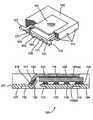
- FIG. 1shows a perspective view of a semiconductor die package. A major surface of a drain clip is exposed through the top side of the package and is parallel to a surface of a molding material.
- FIG. 2shows a perspective bottom view of a semiconductor die package. A major surface of a source lead structure, a surface of a gate lead, and surfaces of source leads are exposed through a molding material.
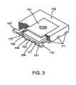
- FIG. 3shows a perspective three dimensional view of a semiconductor die package with part of the molding material partially removed showing a molded assembled part.
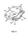
- FIG. 4shows a perspective three dimensional view of a semiconductor die package with part of the molding material partially removed showing a molded assembled part.
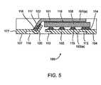
- FIG. 5shows a side cross-sectional view of a semiconductor die package according to an embodiment of the invention.
- FIG. 6shows a drain lead, a source lead structure, and a gate lead.
- FIG. 7shows an exploded view of a semiconductor die package.
- FIG. 8shows a block diagram of an exemplary method for manufacturing semiconductor die packages according to embodiments of the invention.
- Embodiments of the inventionare directed to semiconductor die packages. They can be made in any suitable manner.
- a semiconductor die with solder bumps on its front sidecan be flipped over and attached to a lead frame.
- the lead framemay be a copper lead frame.
- the bumped semiconductor dieincludes one or more gate solder bumps and source solder bumps.
- a gate solder bumpcan be attached to an isolated gate lead structure of the lead frame, while the source solder bumps are attached to one or more source lead structures in the lead frame.
- the gate and source lead structureseventually form gate and source connections for a MOSFET in the semiconductor die.
- the back side of the semiconductor diewhich corresponds to the drain region of the MOSFET, is electrically coupled to a drain clip.
- the drain clipcan be attached to the back side of the semiconductor die using solder paste.
- the drain clipinterconnects the back side of the semiconductor die to a drain lead structure including drain leads.
- Solder pastee.g., a solder paste alloy
- the drain clip, the solder, and the drain lead structurecan provide a drain connection from the back side of the semiconductor die to the front side of the semiconductor die.
- the source lead structure in the semiconductor die packagemay include a protruding portion with a major surface.
- the source leads of the source lead structure, the gate lead of the gate lead structure, and the major surface of the source lead structureare exposed through a molding material. These surfaces may be within the same plane and may also be co-planar with the surface of the drain leads in the drain lead structure.
- a major surface of a drain clipis exposed through the molding material.
- the semiconductor die packages according to embodiments of the inventioncan have a low overall package resistance (i.e., a low RdSon).
- the drain region in the semiconductor diemay be electrically coupled to a drain clip, and the drain clip may be electrically connected to a drain lead structure with drain leads.
- a source lead structure and a gate lead structurecan be respectively coupled to the source region and the gate region in the semiconductor die. Substantially direct electrical connections are made to the gate, source, and drain regions in the semiconductor die, and this reduces the overall package resistance.
- the semiconductor die packagecan accommodate large semiconductor dies, or small semiconductor dies (e.g., up to 4 mils thick) while providing reliable interconnections.
- embodiments of the inventionare thin.
- the semiconductor die packagecan be as thin as 0.75 mm or less.
- embodiments of the inventionalso exhibit improved thermal performance.
- the improved thermal performancecan be achieved, since a drain clip is exposed and is coplanar with the surface of a molding material in the semiconductor die package. This provides for a natural heat sink in the semiconductor die package.
- the source and the drainare exposed at the same time from the top and bottom of the package in one assembly process.
- the exposed major surfaces of the drain clip and the source lead structurecan serve as a natural cooling means to cool off the semiconductor die when it is operating.
- embodiments of the inventioncan also be manufactured in high volumes. Flip chips, lead frames, a drain clip, and a molding material can be used in embodiments of the invention to facilitate high production volumes.
- FIGS. 1-7illustrate embodiments of the invention.
- like numeralsdesignate like elements.
- FIG. 1is a top, perspective view of a semiconductor die package 100 according to an embodiment of the invention.
- the semiconductor die package 100includes a drain clip 101 and a molding material 102 that is molded around the drain clip 101 . As shown in FIG. 1, a major surface 101 ( a ) of the drain clip 101 is exposed through the molding material 102 .
- the molding material 102may comprise any suitable moldable dielectric material that is known in the art.
- the molding material 102protects the semiconductor die (not shown) inside of the package 100 from any contamination or corrosion from the surrounding environment.
- the molding material 102may first be molded, and then shaped. After molding, the molding material 102 can be sawn off and separated from other semiconductor die packages so that the resulting semiconductor die package is in a block form. Alternatively, the molding material 102 may be molded individually without sawing.
- the semiconductor die 108may include any suitable semiconductor device. Suitable devices include vertical power transistors. Vertical power transistors include VDMOS transistors.
- VDMOS transistorsinclude VDMOS transistors.
- a VDMOS transistoris a MOSFET that has two or more semiconductor regions formed by diffusion. It has a source region, a drain region, and a gate region. The device is vertical in that the source region and the drain region are at opposite surfaces of the semiconductor die.
- the gate regionmay be a trenched gate structure or a planar gate structure, and is formed at the same surface as the source region. Trenched gate structures are preferred, since trenched gate structures are narrower and occupy less space than planar gate structures.
- the current flow from the source region to the drain region in a VDMOS deviceis substantially perpendicular to the die surfaces.
- the front side of a semiconductor diecan comprise a source region and a gate region, while the back side of the semiconductor die can comprise the drain region.
- FIG. 2shows the bottom part of a semiconductor die package 100 .
- the semiconductor die package 100includes drain leads 107 .
- the drain leads 107 , and the gate lead 112 and the source leads 111are at opposite sides of the semiconductor die package 100 in the illustrated embodiment.
- a major surface 103 ( a ) of a source lead structure 103is exposed through the molding material 102 .
- the drain leads 107are also exposed through the molding material 102 .
- the drain leads 107 , the gate lead 112 , and the source leads 111do not extend beyond the side surfaces of the molding material 102 . This results in a more compact semiconductor die package.
- Tie bar regions 106are between the source and gate leads 111 , 112 , and the drain leads 107 . When the tie bar regions 106 are uncut, the tie bar regions 106 connect a lead frame containing source and gate leads 111 , 112 and drain leads 107 to other lead frames in an array of lead frames. The tie bar regions 106 serve to support a lead frame before and during package assembly.
- FIG. 3shows an assembled cut-away top view of a semiconductor die package 100 according to an embodiment of the invention.
- a semiconductor die 108is attached to a die attach surface 109 of a source lead structure 103 .
- the source lead structure 103also includes a tie bar region 106 .
- a gate lead structure 171 with a gate lead 112is attached to the gate region (not shown) of the semiconductor die 108 through a solder bump 141 .
- a drain clip 101is attached to the semiconductor die 108 through a layer of solder (not shown).
- the drain clip 101has a major surface 101 ( a ).
- a drain lead structure 177 including drain leads 107is also attached to the drain clip 101 through a layer of solder.
- Source leads 111are shown as being exposed at a side of the semiconductor die package 100 .
- FIG. 4shows an assembled cut-away bottom view of a semiconductor die package 100 .
- the bottom, cut-away portionshows the exposed major surface 103 ( a ) of the source lead structure 103 .
- the major surface 103 ( a )can be directly coupled to a printed circuit board (PCB) (not shown).
- PCBprinted circuit board
- the surfaces of the drain leads 107are shown as being co-planar with the surfaces of the source leads 111 and the gate lead 112 , as well as the major surface 103 ( a ).
- the major surface 103 ( a )is part of a protruding portion of the source lead structure 103 that protrudes from an adjacent surface 113 .
- the adjacent surface 113can be formed by etching.
- the lead frame that is used to form the gate lead structure and the source lead structureis partially-etched (e.g., half-etched) to allow for a molding material to flow during molding.
- the partially etched areaprovides enough area for a mold compound to flow and hold the assembled die package in tact and protected after molding. Partial etching can be performed using photolithography and etching processes that are known in the art. For example, a patterned photoresist layer may be formed on desired areas of a lead frame.
- the lead framecan then be etched (using, for example, wet or dry etching) to a predetermined depth, so that the lead frame is partially etched in some regions.
- FIG. 5shows a side, cross-sectional view of a semiconductor die package according to an embodiment of the invention.
- the drain clip 101is bent at about a 45 degree angle and has a bent portion 117 .
- This drain clip 101is electrically coupled to the backside of the semiconductor die 108 with a layer of eutectic solder paste 116 .
- the drain clip 101has a major surface that is exposed through the molding material 102 .
- the drain clip 101is electrically coupled with the drain lead structure 177 which has a bent portion 120 that forms a V-shape with a main portion of the drain clip 101 .
- Eutectic solder paste 118connects the drain clip 101 to the drain lead structure 120 .
- the drain lead structure 120is partially-etched at reference numeral 119 to allow for the bending of the drain clip 101 .
- the bottom portion of the source lead structure 103also includes a partially etched region 113 .
- the purpose of the partially-etched source lead structure 103is to allow the molding material to flow and hold the semiconductor die package 100 intact and protected.
- the footprint of the semiconductor die package 100is shown by the reference numerals 104 , 107 .
- Flip chip solder bumps 115 and reflowed solder paste 114electrically couple the source lead structure 103 and the semiconductor die 108 together.
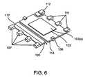
- FIG. 6shows a detailed design of a lead frame structure.
- the isolated gate lead 112is partially-etched to provide enough area for a molding material to flow over it.
- the source leads 111are substantially coplanar with the major surface 103 ( a ) of the source lead structure 103 and can also be formed using a partial etching process.
- the bottom part of the lead frameis partially etched at a region where the adjacent surface 113 is located. The partially-etched region will allow the molding material to flow during molding.
- the drain lead structure 177has drain leads 107 and a bent portion 120 .
- the bent portion 120is where the drain lead structure 177 couples to the drain clip (not shown).
- the drain leads 107can also be formed by partial etching.
- FIG. 7shows an exploded view of a semiconductor die package according to an embodiment of the invention.
- the molding material 102is shown in the final assembly, which holds the various other components in the semiconductor die package together.
- the metallized drain lead structure 177 and the source lead structure 103serve as the drain and source terminals of the semiconductor die package.
- the semiconductor die 108is bumped with solder and this is directly attached to the source lead structure 103 .
- the drain clip 101can be a shaped copper sheet that connects the drain region of the semiconductor die 108 to the drain lead structure 177 .
- the end part of the drain clip 101is bent at a 45 degree angle to match the angular bend of the drain lead structure 177 .
- the angular parts of both the drain lead structure 177 and the drain clip 101are electrically coupled using solder paste. Although 45 degree bend angles are described above, it is understood that the drain lead structure 177 and the drain clip 101 can have bend angles of any appropriate value.
- the semiconductor die packages according to embodiments of the inventionmay be of any suitable size.
- the package sizemay be smaller than 2 ⁇ 2 mm 2 , or could be larger than 20 ⁇ 20 mm 2 .
- the semiconductor die packages according to embodiments of the inventionare preferably cubic in nature. They can sometimes be referred to as “flip chip quad packs.”
- the semiconductor die packages according to embodiments of the inventionmay be manufactured according to any suitable method.
- the methodcomprises providing a semiconductor die comprising a first surface, a second surface, and a vertical power MOSFET having a gate region and a source region at the first surface, and a drain region at the second surface. Then, a source lead structure is attached to the source region and a gate lead to the gate region. A drain clip having a major surface is also attached to the drain region. A molding material is molded around the semiconductor die, whereby the major surface is exposed through the molding material.
- FIG. 8An exemplary process flow is shown in FIG. 8 .
- a semiconductor die with solder bumpsis attached to a lead frame (including what will be the source lead structure, the gate lead structure, and the drain lead structure) in the semiconductor die package using a flip chip die attach process (step 302 ).
- the lead framemay be in an array of lead frames.
- the lead framePrior to solder bump attach, the lead frame may be partially etched in desired regions (as described above), and a portion of the drain lead structure in the lead frame may be bent.
- an infrared (IR) reflow process(step 304 ) is performed to reflow the solder bumps and establish an electrical connection between the semiconductor die and the source lead structure.
- IRinfrared
- a drain clipis then bonded to the semiconductor die (step 306 ).
- the drain clip and/or the semiconductor diemay contain a layer of solder or an array of solder bumps.
- the drain clipcan also be bonded to the drain lead structure in the lead frame with solder.
- the drain clipcan also be bonded to the drain lead structure with solder.
- a film assisted molding processcan then be used to mold a molding material around the semiconductor die, the lead frame structure and the drain clip.
- the filmmay be, for example, a piece of tape that is taped to the major surface of the drain clip.
- the tapeprevents molding material from being deposited on the major surface of the drain clip.
- a molding materialmay be molded around the semiconductor die, the drain clip, and the lead frame structure while the tape is on the drain clip. Excess molding material may be removed from the side of the semiconductor die opposite the drain clip.
- a waterjet deflash process(step 312 ) may be used to remove excess molding material (e.g., on a gate lead structure). Then, the molding material may harden. After molding and deflash, the tape may be removed.
- a laser marking processmay be used to mark the resulting product (step 314 )
- the tie bars (as well as connections to the source leads, gate lead, and drain leads) that hold the lead frame together with other lead framescan be sawed, and the packages in an array can be singulated (step 316 ).
- the final form factor for the package after singulationcan be square in that all sides have leads within the edges of the molding material. Then, the individual semiconductor die packages can be tested (step 318 ).
- drain clipand a drain lead structure as separate elements.
- the drain clipcould include drain leads so that a separate drain lead structure would not be necessary in other embodiments.
Landscapes
- Engineering & Computer Science (AREA)
- Computer Hardware Design (AREA)
- Microelectronics & Electronic Packaging (AREA)
- Power Engineering (AREA)
- Physics & Mathematics (AREA)
- Condensed Matter Physics & Semiconductors (AREA)
- General Physics & Mathematics (AREA)
- Lead Frames For Integrated Circuits (AREA)
- Structures Or Materials For Encapsulating Or Coating Semiconductor Devices Or Solid State Devices (AREA)
Abstract
Description
Claims (14)
Priority Applications (8)
| Application Number | Priority Date | Filing Date | Title |
|---|---|---|---|
| US10/262,170US6777800B2 (en) | 2002-09-30 | 2002-09-30 | Semiconductor die package including drain clip |
| DE10393232TDE10393232T5 (en) | 2002-09-30 | 2003-09-17 | Semiconductor chip package with drain terminal |
| AU2003270700AAU2003270700A1 (en) | 2002-09-30 | 2003-09-17 | Semiconductor die package including drain clip |
| PCT/US2003/029142WO2004032232A1 (en) | 2002-09-30 | 2003-09-17 | Semiconductor die package including drain clip |
| JP2004541558AJP4698225B2 (en) | 2002-09-30 | 2003-09-17 | Semiconductor die package with drain clip |
| CNB038232154ACN100362656C (en) | 2002-09-30 | 2003-09-17 | Semiconductor die package including drain clip |
| TW092126403ATWI319905B (en) | 2002-09-30 | 2003-09-24 | Semiconductor die package including drain clip |
| JP2011004949AJP2011097090A (en) | 2002-09-30 | 2011-01-13 | Semiconductor die package including drain clip |
Applications Claiming Priority (1)
| Application Number | Priority Date | Filing Date | Title |
|---|---|---|---|
| US10/262,170US6777800B2 (en) | 2002-09-30 | 2002-09-30 | Semiconductor die package including drain clip |
Publications (2)
| Publication Number | Publication Date |
|---|---|
| US20040063240A1 US20040063240A1 (en) | 2004-04-01 |
| US6777800B2true US6777800B2 (en) | 2004-08-17 |
Family
ID=32030152
Family Applications (1)
| Application Number | Title | Priority Date | Filing Date |
|---|---|---|---|
| US10/262,170Expired - LifetimeUS6777800B2 (en) | 2002-09-30 | 2002-09-30 | Semiconductor die package including drain clip |
Country Status (7)
| Country | Link |
|---|---|
| US (1) | US6777800B2 (en) |
| JP (2) | JP4698225B2 (en) |
| CN (1) | CN100362656C (en) |
| AU (1) | AU2003270700A1 (en) |
| DE (1) | DE10393232T5 (en) |
| TW (1) | TWI319905B (en) |
| WO (1) | WO2004032232A1 (en) |
Cited By (114)
| Publication number | Priority date | Publication date | Assignee | Title |
|---|---|---|---|---|
| US20040169289A1 (en)* | 2003-02-28 | 2004-09-02 | Yukihiro Satou | Semiconductor device, a method of manufacturing the same and an electronic device |
| US20050001293A1 (en)* | 2001-03-12 | 2005-01-06 | Fairchild Semiconductor Corporation | Method for forming semiconductor device including stacked dies |
| US20050023670A1 (en)* | 2003-07-31 | 2005-02-03 | Renesas Technology Corp. | Semiconductor device and a method of manufacturing the same |
| US6872599B1 (en)* | 2002-12-10 | 2005-03-29 | National Semiconductor Corporation | Enhanced solder joint strength and ease of inspection of leadless leadframe package (LLP) |
| US20050127483A1 (en)* | 2001-10-22 | 2005-06-16 | Rajeev Joshi | Thin, thermally enhanced flip chip in a leaded molded package |
| US20050218498A1 (en)* | 2004-03-09 | 2005-10-06 | Toshiyuki Hata | Semiconductor device |
| US20050218300A1 (en)* | 2004-04-02 | 2005-10-06 | Quinones Maria Clemens Y | Surface mount multi-channel optocoupler |
| US20060097366A1 (en)* | 2003-07-19 | 2006-05-11 | Ns Electronics Bangkok (1993) Ltd. | Semiconductor package including leadframe roughened with chemical etchant to prevent separation between leadframe and molding compound |
| US20060108671A1 (en)* | 2004-11-23 | 2006-05-25 | Siliconix Incorporated | Semiconductor package including die interposed between cup-shaped lead frame and lead frame having mesas and valleys |
| US20060110856A1 (en)* | 2004-11-23 | 2006-05-25 | Mohammed Kasem | Method of fabricating semiconductor package including die interposed between cup-shaped lead frame having mesas and valleys |
| US20060145312A1 (en)* | 2005-01-05 | 2006-07-06 | Kai Liu | Dual flat non-leaded semiconductor package |
| US20060237814A1 (en)* | 2005-03-09 | 2006-10-26 | Khalil Hosseini | Semiconductor device having surface mountable external contact areas and method for producing the same |
| US20060267161A1 (en)* | 2005-05-31 | 2006-11-30 | Thompson Vasile R | Methods of making integrated circuits |
| US20070001278A1 (en)* | 2005-06-30 | 2007-01-04 | Oseob Jeon | Semiconductor die package and method for making the same |
| US20070040252A1 (en)* | 2005-08-17 | 2007-02-22 | Khalil Hosseini | Semiconductor power component with a vertical current path through a semiconductor power chip |
| US20070045785A1 (en)* | 2005-08-30 | 2007-03-01 | Noquil Jonathan A | Reversible-multiple footprint package and method of manufacturing |
| US20070090463A1 (en)* | 2005-10-20 | 2007-04-26 | Tan Xiaochun | Semiconductor devices with multiple heat sinks |
| US20070090523A1 (en)* | 2005-10-20 | 2007-04-26 | Ralf Otremba | Semiconductor component and methods to produce a semiconductor component |
| US20070114352A1 (en)* | 2005-11-18 | 2007-05-24 | Victor R Cruz Erwin | Semiconductor die package using leadframe and clip and method of manufacturing |
| US20070155058A1 (en)* | 2006-01-05 | 2007-07-05 | Jereza Armand Vincent C | Clipless and wireless semiconductor die package and method for making the same |
| US20070161151A1 (en)* | 2005-12-30 | 2007-07-12 | Madrid Ruben P | Packaged semiconductor device with dual exposed surfaces and method of manufacturing |
| US20070164428A1 (en)* | 2006-01-18 | 2007-07-19 | Alan Elbanhawy | High power module with open frame package |
| US20070187807A1 (en)* | 2006-02-13 | 2007-08-16 | Jeongil Lee | Multi-chip module for battery power control |
| US20070222044A1 (en)* | 2006-03-21 | 2007-09-27 | Ralf Otremba | Electronic Component and Methods to Produce an Electronic Component |
| US20070249092A1 (en)* | 2006-04-24 | 2007-10-25 | Rajeev Joshi | Semiconductor die package including multiple dies and a common node structure |
| US20070259514A1 (en)* | 2006-05-04 | 2007-11-08 | Ralf Otremba | Interconnection Structure, Electronic Component and Method of Manufacturing the Same |
| US20070267728A1 (en)* | 2006-05-19 | 2007-11-22 | Noquil Jonathan A | Flip chip mlp with folded heat sink |
| US20070267729A1 (en)* | 2006-05-17 | 2007-11-22 | Ralf Otremba | Electronic Component Having a Semiconductor Power Device |
| US20070290337A1 (en)* | 2006-06-14 | 2007-12-20 | Ralf Otremba | Electrically Conductive Connection, Electronic Component and Method for Their Production |
| US20080001279A1 (en)* | 2006-06-30 | 2008-01-03 | Alan Elbanhawy | Chip module for complete power train |
| US20080048342A1 (en)* | 2006-04-28 | 2008-02-28 | Chuan Cheah | Multi-chip module |
| US20080054417A1 (en)* | 2006-08-29 | 2008-03-06 | Sangdo Lee | Semiconductor die package including stacked dice and heat sink structures |
| US20080173991A1 (en)* | 2007-01-24 | 2008-07-24 | Erwin Victor Cruz | Pre-molded clip structure |
| US20080185696A1 (en)* | 2007-02-05 | 2008-08-07 | Ruben Madrid | Semiconductor die package including leadframe with die attach pad with folded edge |
| US20080203550A1 (en)* | 2007-02-27 | 2008-08-28 | Henrik Ewe | Component, Power Component, Apparatus, Method Of Manufacturing A Component, And Method Of Manufacturing A Power Semiconductor Component |
| US20080203559A1 (en)* | 2007-02-28 | 2008-08-28 | Lee Keun-Hyuk | Power device package and semiconductor package mold for fabricating the same |
| US20080209511A1 (en)* | 2004-05-18 | 2008-08-28 | Silverbrook Research Pty Ltd | Authentication method for pharmaceutical products having coded packaging |
| US20080211070A1 (en)* | 2004-11-23 | 2008-09-04 | Ming Sun | Flip chip contact (FCC) power package |
| US20080224285A1 (en)* | 2007-03-12 | 2008-09-18 | Lim Seung-Won | Power module having stacked flip-chip and method of fabricating the power module |
| US20080224286A1 (en)* | 2007-03-13 | 2008-09-18 | Martin Standing | Vertically mountable semiconductor device package |
| US20080246137A1 (en)* | 2006-10-19 | 2008-10-09 | Infineon Technologies Ag | Integrated circuit device and method for the production thereof |
| US20080251739A1 (en)* | 2007-04-13 | 2008-10-16 | Yoon Hwa Choi | Optical coupler package |
| US20080258272A1 (en)* | 2007-04-19 | 2008-10-23 | Lay Yeap Lim | Etched leadframe structure |
| US20080271585A1 (en)* | 2007-05-05 | 2008-11-06 | Jones Pearl R | Apparatus and method for teaching the playing of a stringed instrument |
| US20090008758A1 (en)* | 2005-01-05 | 2009-01-08 | Alpha & Omega Semiconductor Incorporated | Use of discrete conductive layer in semiconductor device to re-route bonding wires for semiconductor device package |
| US20090057852A1 (en)* | 2007-08-27 | 2009-03-05 | Madrid Ruben P | Thermally enhanced thin semiconductor package |
| US20090057854A1 (en)* | 2007-08-28 | 2009-03-05 | Gomez Jocel P | Self locking and aligning clip structure for semiconductor die package |
| US20090057855A1 (en)* | 2007-08-30 | 2009-03-05 | Maria Clemens Quinones | Semiconductor die package including stand off structures |
| WO2006058030A3 (en)* | 2004-11-23 | 2009-04-02 | Siliconix Inc | Semiconductor package including die interposed between cup-shaped lead frame and lead frame having mesas and valleys |
| US20090128968A1 (en)* | 2007-11-21 | 2009-05-21 | Alpha & Omega Semiconductor, Ltd. | Stacked-die package for battery power management |
| US20090140179A1 (en)* | 2007-11-30 | 2009-06-04 | Yong Liu | Semiconductor die packages suitable for optoelectronic applications having clip attach structures for angled mounting of dice |
| US20090140266A1 (en)* | 2007-11-30 | 2009-06-04 | Yong Liu | Package including oriented devices |
| US20090146284A1 (en)* | 2007-12-06 | 2009-06-11 | Kim Ji-Hwan | Molded Leadless Packages and Assemblies Having Stacked Molded Leadless Packages |
| US20090160036A1 (en)* | 2007-12-19 | 2009-06-25 | David Grey | Package with multiple dies |
| US20090166850A1 (en)* | 2008-01-02 | 2009-07-02 | Oseob Jeon | High-Power Semiconductor Die Packages With Integrated Heat-Sink Capability and Methods of Manufacturing the Same |
| US20090166826A1 (en)* | 2007-12-27 | 2009-07-02 | Janducayan Omar A | Lead frame die attach paddles with sloped walls and backside grooves suitable for leadless packages |
| US20090174044A1 (en)* | 2007-12-13 | 2009-07-09 | Eom Joo-Yang | Multi-chip package |
| US20090174048A1 (en)* | 2008-01-09 | 2009-07-09 | Yong Liu | Die package including substrate with molded device |
| US20090179315A1 (en)* | 2008-01-14 | 2009-07-16 | Armand Vincent Jereza | Semiconductor Die Packages Having Solder-free Connections, Systems Using the Same, and Methods of Making the Same |
| US20090179313A1 (en)* | 2008-01-10 | 2009-07-16 | Maria Clemens Quinones | Flex clip connector for semiconductor device |
| US20090194856A1 (en)* | 2008-02-06 | 2009-08-06 | Gomez Jocel P | Molded package assembly |
| US20090218666A1 (en)* | 2008-02-28 | 2009-09-03 | Yang Gwi-Gyeon | Power device package and method of fabricating the same |
| USD600219S1 (en)* | 2006-04-26 | 2009-09-15 | Panasonic Corporation | Lead frame |
| US20090230519A1 (en)* | 2008-03-14 | 2009-09-17 | Infineon Technologies Ag | Semiconductor Device |
| US20090230536A1 (en)* | 2008-03-12 | 2009-09-17 | Yong Liu | Semiconductor die package including multiple semiconductor dice |
| US20090243079A1 (en)* | 2008-03-31 | 2009-10-01 | Lim Seung-Won | Semiconductor device package |
| US20090278241A1 (en)* | 2008-05-08 | 2009-11-12 | Yong Liu | Semiconductor die package including die stacked on premolded substrate including die |
| US20090294934A1 (en)* | 2008-05-30 | 2009-12-03 | Alpha & Omega Semiconductor, Ltd. | Conductive clip for semiconductor device package |
| US20100052119A1 (en)* | 2008-08-28 | 2010-03-04 | Yong Liu | Molded Ultra Thin Semiconductor Die Packages, Systems Using the Same, and Methods of Making the Same |
| US20100072585A1 (en)* | 2008-09-25 | 2010-03-25 | Alpha & Omega Semiconductor Incorporated | Top exposed clip with window array |
| US20100072590A1 (en)* | 2008-09-22 | 2010-03-25 | Yong Liu | Stacking Quad Pre-Molded Component Packages, Systems Using the Same, and Methods of Making the Same |
| US20100078831A1 (en)* | 2008-09-26 | 2010-04-01 | Jairus Legaspi Pisigan | Integrated circuit package system with singulation process |
| US20100109134A1 (en)* | 2008-10-31 | 2010-05-06 | Jereza Armand Vincent C | Pre-molded, clip-bonded multi-die semiconductor package |
| US20100109147A1 (en)* | 2008-11-06 | 2010-05-06 | Tracy Autry | Less expensive high power plastic surface mount package |
| US20100123257A1 (en)* | 2008-11-14 | 2010-05-20 | Yong Liu | Flexible and Stackable Semiconductor Die Packages, Systems Using the Same, and Methods of Making the Same |
| US7737548B2 (en) | 2007-08-29 | 2010-06-15 | Fairchild Semiconductor Corporation | Semiconductor die package including heat sinks |
| US20100148346A1 (en)* | 2008-12-12 | 2010-06-17 | Quinones Maria Clemens Y | Semiconductor die package including low stress configuration |
| US20100148328A1 (en)* | 2008-12-17 | 2010-06-17 | Fairchild Semiconductor Corporation | Power quad flat no-lead semiconductor die packages with isolated heat sink for high-voltage, high-power applications, systems using the same, and methods of making the same |
| US20100176508A1 (en)* | 2009-01-12 | 2010-07-15 | Ciclon Semiconductor Device Corp. | Semiconductor device package and method of assembly thereof |
| US7757392B2 (en) | 2006-05-17 | 2010-07-20 | Infineon Technologies Ag | Method of producing an electronic component |
| US20100181666A1 (en)* | 2009-01-16 | 2010-07-22 | Nec Electronics Corporation | Semiconductor device having lead free solders between semiconductor chip and frame and gabrication method thereof |
| US7768075B2 (en) | 2006-04-06 | 2010-08-03 | Fairchild Semiconductor Corporation | Semiconductor die packages using thin dies and metal substrates |
| US7768108B2 (en) | 2008-03-12 | 2010-08-03 | Fairchild Semiconductor Corporation | Semiconductor die package including embedded flip chip |
| US20100193921A1 (en)* | 2009-02-05 | 2010-08-05 | Jereza Armand Vincent C | Semiconductor die package and method for making the same |
| US20100193803A1 (en)* | 2009-02-04 | 2010-08-05 | Yong Liu | Stacked Micro Optocouplers and Methods of Making the Same |
| US7791084B2 (en) | 2008-01-09 | 2010-09-07 | Fairchild Semiconductor Corporation | Package with overlapping devices |
| US7851897B1 (en)* | 2008-06-16 | 2010-12-14 | Maxim Integrated Products, Inc. | IC package structures for high power dissipation and low RDSon |
| US20110024917A1 (en)* | 2009-07-31 | 2011-02-03 | Anup Bhalla | Multi-die package |
| US20110033977A1 (en)* | 2009-08-06 | 2011-02-10 | Maxim Integrated Products, Inc. | Method of forming solderable side-surface terminals of quad no-lead frame (qfn) integrated circuit packages |
| US20110095411A1 (en)* | 2006-08-14 | 2011-04-28 | Texas Instruments Incorporated | Wirebond-less Semiconductor Package |
| US20110227207A1 (en)* | 2010-03-18 | 2011-09-22 | Alpha And Omega Semiconductor Incorporated | Stacked dual chip package and method of fabrication |
| US20110227205A1 (en)* | 2010-03-18 | 2011-09-22 | Jun Lu | Multi-layer lead frame package and method of fabrication |
| US20120032317A1 (en)* | 2007-11-08 | 2012-02-09 | Randolph Cruz | Self-Aligning Structures and Method for Integrated Chips |
| US20120104580A1 (en)* | 2010-10-29 | 2012-05-03 | Alpha And Omega Semiconductor Incorporated | Substrateless power device packages |
| US8193618B2 (en) | 2008-12-12 | 2012-06-05 | Fairchild Semiconductor Corporation | Semiconductor die package with clip interconnection |
| US8421204B2 (en) | 2011-05-18 | 2013-04-16 | Fairchild Semiconductor Corporation | Embedded semiconductor power modules and packages |
| US8436429B2 (en) | 2011-05-29 | 2013-05-07 | Alpha & Omega Semiconductor, Inc. | Stacked power semiconductor device using dual lead frame and manufacturing method |
| US8531016B2 (en)* | 2011-05-19 | 2013-09-10 | International Rectifier Corporation | Thermally enhanced semiconductor package with exposed parallel conductive clip |
| TWI419286B (en)* | 2010-12-14 | 2013-12-11 | Alpha & Omega Semiconductor | Top exposed package and assembly method |
| US20140273344A1 (en)* | 2013-03-14 | 2014-09-18 | Vishay-Siliconix | Method for fabricating stack die package |
| US20150173248A1 (en)* | 2013-12-16 | 2015-06-18 | Delta Electronics (Shanghai) Co., Ltd. | Power module, power converter and manufacturing method of power module |
| US9070721B2 (en) | 2013-03-15 | 2015-06-30 | Semiconductor Components Industries, Llc | Semiconductor devices and methods of making the same |
| US20150214139A1 (en)* | 2014-01-30 | 2015-07-30 | Kabushiki Kaisha Toshiba | Semiconductor device |
| US9184152B2 (en) | 2010-09-09 | 2015-11-10 | Vishay-Siliconix | Dual lead frame semiconductor package and method of manufacture |
| US9257375B2 (en) | 2009-07-31 | 2016-02-09 | Alpha and Omega Semiconductor Inc. | Multi-die semiconductor package |
| US9391005B2 (en)* | 2009-10-27 | 2016-07-12 | Alpha And Omega Semiconductor Incorporated | Method for packaging a power device with bottom source electrode |
| US20170263539A1 (en)* | 2013-03-14 | 2017-09-14 | General Electric Company | Power overlay structure and method of making same |
| US9966330B2 (en) | 2013-03-14 | 2018-05-08 | Vishay-Siliconix | Stack die package |
| US10186477B2 (en) | 2013-03-14 | 2019-01-22 | General Electric Company | Power overlay structure and method of making same |
| US11075154B2 (en)* | 2017-10-26 | 2021-07-27 | Shindengen Electric Manufacturing Co., Ltd. | Semiconductor device and method of manufacturing semiconductor device |
| US20220208686A1 (en)* | 2020-12-30 | 2022-06-30 | UTAC Headquarters Pte. Ltd. | Semiconductor Device and Method of Forming Leadframe with Clip Bond for Electrical Interconnect |
| EP4123699A1 (en) | 2021-07-22 | 2023-01-25 | Nexperia B.V. | A semiconductor device and a method of manufacturing of a semiconductor device |
| EP4123700A1 (en) | 2021-07-22 | 2023-01-25 | Nexperia B.V. | A semiconductor device and a method of manufacturing of a semiconductor device |
| EP4148779A1 (en) | 2021-09-14 | 2023-03-15 | Nexperia B.V. | A semiconductor device and a method of manufacture |
Families Citing this family (53)
| Publication number | Priority date | Publication date | Assignee | Title |
|---|---|---|---|---|
| US7122884B2 (en)* | 2002-04-16 | 2006-10-17 | Fairchild Semiconductor Corporation | Robust leaded molded packages and methods for forming the same |
| US7061077B2 (en) | 2002-08-30 | 2006-06-13 | Fairchild Semiconductor Corporation | Substrate based unmolded package including lead frame structure and semiconductor die |
| US6867481B2 (en)* | 2003-04-11 | 2005-03-15 | Fairchild Semiconductor Corporation | Lead frame structure with aperture or groove for flip chip in a leaded molded package |
| DE102004041088B4 (en)* | 2004-08-24 | 2009-07-02 | Infineon Technologies Ag | Semiconductor component in flat conductor technology with a semiconductor chip and method for its production |
| US7812441B2 (en)* | 2004-10-21 | 2010-10-12 | Siliconix Technology C.V. | Schottky diode with improved surge capability |
| TWI278090B (en)* | 2004-10-21 | 2007-04-01 | Int Rectifier Corp | Solderable top metal for SiC device |
| US9419092B2 (en) | 2005-03-04 | 2016-08-16 | Vishay-Siliconix | Termination for SiC trench devices |
| US7834376B2 (en) | 2005-03-04 | 2010-11-16 | Siliconix Technology C. V. | Power semiconductor switch |
| DE102005027356B4 (en)* | 2005-06-13 | 2007-11-22 | Infineon Technologies Ag | Semiconductor power device stack in flat conductor technology with surface-mountable external contacts and a method for producing the same |
| CN101223638A (en)* | 2005-07-05 | 2008-07-16 | 国际整流器公司 | Schottky diode with improved surge capability |
| US8368165B2 (en) | 2005-10-20 | 2013-02-05 | Siliconix Technology C. V. | Silicon carbide Schottky diode |
| US7749877B2 (en)* | 2006-03-07 | 2010-07-06 | Siliconix Technology C. V. | Process for forming Schottky rectifier with PtNi silicide Schottky barrier |
| US7663211B2 (en)* | 2006-05-19 | 2010-02-16 | Fairchild Semiconductor Corporation | Dual side cooling integrated power device package and module with a clip attached to a leadframe in the package and the module and methods of manufacture |
| US9627552B2 (en) | 2006-07-31 | 2017-04-18 | Vishay-Siliconix | Molybdenum barrier metal for SiC Schottky diode and process of manufacture |
| DE102006060484B4 (en)* | 2006-12-19 | 2012-03-08 | Infineon Technologies Ag | Semiconductor device with a semiconductor chip and method for producing the same |
| DE102007002807B4 (en)* | 2007-01-18 | 2014-08-14 | Infineon Technologies Ag | chip system |
| US7872350B2 (en)* | 2007-04-10 | 2011-01-18 | Qimonda Ag | Multi-chip module |
| US7759777B2 (en)* | 2007-04-16 | 2010-07-20 | Infineon Technologies Ag | Semiconductor module |
| US7851908B2 (en)* | 2007-06-27 | 2010-12-14 | Infineon Technologies Ag | Semiconductor device |
| US7705436B2 (en)* | 2007-08-06 | 2010-04-27 | Infineon Technologies Ag | Semiconductor device with semiconductor chip and method for producing it |
| US8129225B2 (en)* | 2007-08-10 | 2012-03-06 | Infineon Technologies Ag | Method of manufacturing an integrated circuit module |
| JP5025394B2 (en)* | 2007-09-13 | 2012-09-12 | 株式会社東芝 | Semiconductor device and manufacturing method thereof |
| US7727813B2 (en) | 2007-11-26 | 2010-06-01 | Infineon Technologies Ag | Method for making a device including placing a semiconductor chip on a substrate |
| EP2242094A1 (en) | 2009-04-17 | 2010-10-20 | Nxp B.V. | Foil and method for foil-based bonding and resulting package |
| US20110095410A1 (en)* | 2009-10-28 | 2011-04-28 | Fairchild Semiconductor Corporation | Wafer level semiconductor device connector |
| US8486757B2 (en) | 2009-11-25 | 2013-07-16 | Infineon Technologies Ag | Semiconductor device and method of packaging a semiconductor device with a clip |
| US8586419B2 (en)* | 2010-01-19 | 2013-11-19 | Vishay-Siliconix | Semiconductor packages including die and L-shaped lead and method of manufacture |
| US8193620B2 (en)* | 2010-02-17 | 2012-06-05 | Analog Devices, Inc. | Integrated circuit package with enlarged die paddle |
| CN101859755B (en)* | 2010-05-14 | 2012-01-04 | 上海凯虹科技电子有限公司 | Power MOSFET (Metal-Oxide-Semiconductor Field Effect Transistor) package body and package method thereof |
| JP5822468B2 (en)* | 2011-01-11 | 2015-11-24 | ローム株式会社 | Semiconductor device |
| US8614503B2 (en)* | 2011-05-19 | 2013-12-24 | International Rectifier Corporation | Common drain exposed conductive clip for high power semiconductor packages |
| CN102842556B (en)* | 2011-06-21 | 2015-04-22 | 万国半导体(开曼)股份有限公司 | Semiconductor component with dual surfaces exposed and manufacturing method of semiconductor component |
| JP5475737B2 (en) | 2011-10-04 | 2014-04-16 | 富士フイルム株式会社 | Radiation imaging apparatus and image processing method |
| CN102842548A (en)* | 2012-08-23 | 2012-12-26 | 苏州固锝电子股份有限公司 | Square flat-type power metal oxide semi-conductor (MOS) chip packaging structure |
| CN103208474A (en)* | 2013-03-22 | 2013-07-17 | 苏州固锝电子股份有限公司 | Quad flat type high-power chip packing structure |
| CN104347568B (en)* | 2013-08-07 | 2017-03-01 | 万国半导体股份有限公司 | Semiconductor device of multi-chip hybrid packaged and preparation method thereof |
| JP6386746B2 (en) | 2014-02-26 | 2018-09-05 | 株式会社ジェイデバイス | Semiconductor device |
| US9425304B2 (en) | 2014-08-21 | 2016-08-23 | Vishay-Siliconix | Transistor structure with improved unclamped inductive switching immunity |
| KR20160033870A (en)* | 2014-09-18 | 2016-03-29 | 제엠제코(주) | Semiconductor package with clip structure |
| CN106158734B (en)* | 2014-10-03 | 2019-01-08 | 力祥半导体股份有限公司 | Semiconductor packaging device |
| JP2016149516A (en)* | 2015-02-05 | 2016-08-18 | 株式会社東芝 | Semiconductor device |
| US10256168B2 (en)* | 2016-06-12 | 2019-04-09 | Nexperia B.V. | Semiconductor device and lead frame therefor |
| US10727151B2 (en)* | 2017-05-25 | 2020-07-28 | Infineon Technologies Ag | Semiconductor chip package having a cooling surface and method of manufacturing a semiconductor package |
| JP6892796B2 (en) | 2017-07-07 | 2021-06-23 | 新光電気工業株式会社 | Electronic component equipment and its manufacturing method |
| US10672691B2 (en)* | 2017-12-18 | 2020-06-02 | Littelfuse, Inc. | Thin profile power semiconductor device package having face-to-face mounted dice and no internal bondwires |
| DE102017223689B4 (en)* | 2017-12-22 | 2024-06-13 | Infineon Technologies Ag | Semiconductor devices with high frequency conduction elements and related manufacturing processes |
| EP3882969B1 (en)* | 2020-03-18 | 2024-05-01 | Nexperia B.V. | A cascode semiconductor device and method of manufacture |
| JP6967627B2 (en) | 2020-05-08 | 2021-11-17 | アオイ電子株式会社 | Semiconductor device |
| US11562949B2 (en)* | 2020-06-17 | 2023-01-24 | Texas Instruments Incorporated | Semiconductor package including undermounted die with exposed backside metal |
| CN112151466B (en)* | 2020-09-07 | 2023-06-27 | 矽磐微电子(重庆)有限公司 | Chip packaging structure and manufacturing method thereof |
| JP2024046340A (en)* | 2022-09-22 | 2024-04-03 | 株式会社東芝 | Semiconductor Device |
| TWI875286B (en)* | 2023-11-03 | 2025-03-01 | 同欣電子工業股份有限公司 | Semiconductor package structure |
| CN117476590A (en)* | 2023-12-28 | 2024-01-30 | 华羿微电子股份有限公司 | Double-sided heat dissipation packaging structure and preparation method thereof |
Citations (15)
| Publication number | Priority date | Publication date | Assignee | Title |
|---|---|---|---|---|
| US5319242A (en) | 1992-03-18 | 1994-06-07 | Motorola, Inc. | Semiconductor package having an exposed die surface |
| US6133634A (en) | 1998-08-05 | 2000-10-17 | Fairchild Semiconductor Corporation | High performance flip chip package |
| US6143981A (en) | 1998-06-24 | 2000-11-07 | Amkor Technology, Inc. | Plastic integrated circuit package and method and leadframe for making the package |
| US20010048116A1 (en)* | 2000-04-04 | 2001-12-06 | International Rectifier Corp. | Chip scale surface mounted device and process of manufacture |
| US20020066950A1 (en) | 2000-12-04 | 2002-06-06 | Fairchild Semiconductor Corporation | Flip chip in leaded molded package with two dies |
| US20020081772A1 (en) | 2000-12-21 | 2002-06-27 | Madrid Ruben P. | Method and system for manufacturing ball grid array ("BGA") packages |
| US20020089042A1 (en) | 2000-11-28 | 2002-07-11 | Madrid Ruben P. | Semiconductor leadframe for staggered board attach |
| US20020100962A1 (en) | 2001-02-01 | 2002-08-01 | Rajeev Joshi | Unmolded package for a semiconductor device |
| US20020125550A1 (en)* | 2001-03-12 | 2002-09-12 | Estacio Maria Cristina B. | Dual stacked die package |
| US20020167075A1 (en) | 2001-05-14 | 2002-11-14 | Ruben Madrid | Carrier with metal bumps for semiconductor die packages |
| US20020171126A1 (en) | 2001-05-15 | 2002-11-21 | Estacio Maria Cristina B. | Power chip scale package |
| US20030025183A1 (en)* | 2001-08-01 | 2003-02-06 | Fairchild Semiconductor Corporation | Packaged semiconductor device and method of manufacture using shaped die |
| US20030052408A1 (en)* | 2000-04-13 | 2003-03-20 | Fairchild Semiconductor Corporation | Semiconductor device including molded wireless exposed drain packaging |
| US20030197278A1 (en)* | 2002-04-17 | 2003-10-23 | Rajeev Joshi | Structure of integrated trace of chip package |
| US6674157B2 (en) | 2001-11-02 | 2004-01-06 | Fairchild Semiconductor Corporation | Semiconductor package comprising vertical power transistor |
Family Cites Families (4)
| Publication number | Priority date | Publication date | Assignee | Title |
|---|---|---|---|---|
| JP3867881B2 (en)* | 1998-09-09 | 2007-01-17 | 新電元工業株式会社 | Semiconductor device |
| JP4260263B2 (en)* | 1999-01-28 | 2009-04-30 | 株式会社ルネサステクノロジ | Semiconductor device |
| JP3596388B2 (en)* | 1999-11-24 | 2004-12-02 | 株式会社デンソー | Semiconductor device |
| US6870254B1 (en)* | 2000-04-13 | 2005-03-22 | Fairchild Semiconductor Corporation | Flip clip attach and copper clip attach on MOSFET device |
- 2002
- 2002-09-30USUS10/262,170patent/US6777800B2/ennot_activeExpired - Lifetime
- 2003
- 2003-09-17WOPCT/US2003/029142patent/WO2004032232A1/enactiveApplication Filing
- 2003-09-17DEDE10393232Tpatent/DE10393232T5/ennot_activeCeased
- 2003-09-17AUAU2003270700Apatent/AU2003270700A1/ennot_activeAbandoned
- 2003-09-17JPJP2004541558Apatent/JP4698225B2/ennot_activeExpired - Fee Related
- 2003-09-17CNCNB038232154Apatent/CN100362656C/ennot_activeExpired - Fee Related
- 2003-09-24TWTW092126403Apatent/TWI319905B/ennot_activeIP Right Cessation
- 2011
- 2011-01-13JPJP2011004949Apatent/JP2011097090A/enactivePending
Patent Citations (18)
| Publication number | Priority date | Publication date | Assignee | Title |
|---|---|---|---|---|
| US5319242A (en) | 1992-03-18 | 1994-06-07 | Motorola, Inc. | Semiconductor package having an exposed die surface |
| US6143981A (en) | 1998-06-24 | 2000-11-07 | Amkor Technology, Inc. | Plastic integrated circuit package and method and leadframe for making the package |
| US6489678B1 (en) | 1998-08-05 | 2002-12-03 | Fairchild Semiconductor Corporation | High performance multi-chip flip chip package |
| US6133634A (en) | 1998-08-05 | 2000-10-17 | Fairchild Semiconductor Corporation | High performance flip chip package |
| US20010048116A1 (en)* | 2000-04-04 | 2001-12-06 | International Rectifier Corp. | Chip scale surface mounted device and process of manufacture |
| US6624522B2 (en)* | 2000-04-04 | 2003-09-23 | International Rectifier Corporation | Chip scale surface mounted device and process of manufacture |
| US20030052408A1 (en)* | 2000-04-13 | 2003-03-20 | Fairchild Semiconductor Corporation | Semiconductor device including molded wireless exposed drain packaging |
| US20020089042A1 (en) | 2000-11-28 | 2002-07-11 | Madrid Ruben P. | Semiconductor leadframe for staggered board attach |
| US20020066950A1 (en) | 2000-12-04 | 2002-06-06 | Fairchild Semiconductor Corporation | Flip chip in leaded molded package with two dies |
| US20020081772A1 (en) | 2000-12-21 | 2002-06-27 | Madrid Ruben P. | Method and system for manufacturing ball grid array ("BGA") packages |
| US6469384B2 (en) | 2001-02-01 | 2002-10-22 | Fairchild Semiconductor Corporation | Unmolded package for a semiconductor device |
| US20020100962A1 (en) | 2001-02-01 | 2002-08-01 | Rajeev Joshi | Unmolded package for a semiconductor device |
| US20020125550A1 (en)* | 2001-03-12 | 2002-09-12 | Estacio Maria Cristina B. | Dual stacked die package |
| US20020167075A1 (en) | 2001-05-14 | 2002-11-14 | Ruben Madrid | Carrier with metal bumps for semiconductor die packages |
| US20020171126A1 (en) | 2001-05-15 | 2002-11-21 | Estacio Maria Cristina B. | Power chip scale package |
| US20030025183A1 (en)* | 2001-08-01 | 2003-02-06 | Fairchild Semiconductor Corporation | Packaged semiconductor device and method of manufacture using shaped die |
| US6674157B2 (en) | 2001-11-02 | 2004-01-06 | Fairchild Semiconductor Corporation | Semiconductor package comprising vertical power transistor |
| US20030197278A1 (en)* | 2002-04-17 | 2003-10-23 | Rajeev Joshi | Structure of integrated trace of chip package |
Non-Patent Citations (2)
| Title |
|---|
| Fairchild Semiconductor Catalog "High Speed-10 MBit/s Logic Gate Optocouplers," Aug. 27, 2002, pp. 1-11. |
| Seme Lab Catalog "Metal Gate RF Silicon FET," 1996, pp. 1-2. |
Cited By (264)
| Publication number | Priority date | Publication date | Assignee | Title |
|---|---|---|---|---|
| US7071033B2 (en)* | 2001-03-12 | 2006-07-04 | Fairchild Semiconductor Corporation | Method for forming semiconductor device including stacked dies |
| US20050001293A1 (en)* | 2001-03-12 | 2005-01-06 | Fairchild Semiconductor Corporation | Method for forming semiconductor device including stacked dies |
| US7821124B2 (en) | 2001-10-22 | 2010-10-26 | Fairchild Semiconductor Corporation | Thin, thermally enhanced flip chip in a leaded molded package |
| US20050127483A1 (en)* | 2001-10-22 | 2005-06-16 | Rajeev Joshi | Thin, thermally enhanced flip chip in a leaded molded package |
| US7332806B2 (en)* | 2001-10-22 | 2008-02-19 | Fairchild Semiconductor Corporation | Thin, thermally enhanced molded package with leadframe having protruding region |
| US20080105957A1 (en)* | 2001-10-22 | 2008-05-08 | Rajeev Joshi | Thin, thermally enhanced flip chip in a leaded molded package |
| US7023074B2 (en) | 2002-12-10 | 2006-04-04 | National Semiconductor Corporation | Enhanced solder joint strength and ease of inspection of leadless leadframe package (LLP) |
| US20050116321A1 (en)* | 2002-12-10 | 2005-06-02 | National Semiconductor Corporation, A Delaware Corp. | Enhanced solder joint strength and ease of inspection of leadless leadframe package (LLP) |
| US6872599B1 (en)* | 2002-12-10 | 2005-03-29 | National Semiconductor Corporation | Enhanced solder joint strength and ease of inspection of leadless leadframe package (LLP) |
| US20050218494A1 (en)* | 2003-02-28 | 2005-10-06 | Renesas Technology Corp. | Semiconductor device, a method of manufacturing the same and an electronic device |
| US6992385B2 (en)* | 2003-02-28 | 2006-01-31 | Renesas Technology Corp. | Semiconductor device, a method of manufacturing the same and an electronic device |
| US7728416B2 (en) | 2003-02-28 | 2010-06-01 | Renesas Technology Corp. | Semiconductor device, a method of manufacturing the same and an electronic device |
| US20090001559A1 (en)* | 2003-02-28 | 2009-01-01 | Renesas Technology Corp. | Semiconductor device, a method of manufacturing the same and an electronic device |
| US20100193934A1 (en)* | 2003-02-28 | 2010-08-05 | Renesas Technology Corp. | Semiconductor device, a method of manufacturing the same and an electronic device |
| US20040169289A1 (en)* | 2003-02-28 | 2004-09-02 | Yukihiro Satou | Semiconductor device, a method of manufacturing the same and an electronic device |
| US8022518B2 (en) | 2003-02-28 | 2011-09-20 | Renesas Electronics Corporation | Semiconductor device having a sealing body and partially exposed conductors |
| US8698289B2 (en) | 2003-02-28 | 2014-04-15 | Renesas Electronics Corporation | Semiconductor device, a method of manufacturing the same and an electronic device |
| US7205180B1 (en) | 2003-07-19 | 2007-04-17 | Ns Electronics Bangkok (1993) Ltd. | Process of fabricating semiconductor packages using leadframes roughened with chemical etchant |
| US20060097366A1 (en)* | 2003-07-19 | 2006-05-11 | Ns Electronics Bangkok (1993) Ltd. | Semiconductor package including leadframe roughened with chemical etchant to prevent separation between leadframe and molding compound |
| US7049683B1 (en)* | 2003-07-19 | 2006-05-23 | Ns Electronics Bangkok (1993) Ltd. | Semiconductor package including organo-metallic coating formed on surface of leadframe roughened using chemical etchant to prevent separation between leadframe and molding compound |
| US7327017B2 (en) | 2003-07-19 | 2008-02-05 | Utac Thai Limited | Semiconductor package including leadframe roughened with chemical etchant to prevent separation between leadframe and molding compound |
| US7586180B2 (en) | 2003-07-31 | 2009-09-08 | Renesas Technology Corp. | Semiconductor packaging device comprising a semiconductor chip including a MOSFET |
| US7408251B2 (en)* | 2003-07-31 | 2008-08-05 | Renesas Technology Corp. | Semiconductor packaging device comprising a semiconductor chip including a MOSFET |
| US20080272472A1 (en)* | 2003-07-31 | 2008-11-06 | Renesas Technology Corp. | Semiconductor packaging device comprising a semiconductor chip including a MOSFET |
| US20060097391A1 (en)* | 2003-07-31 | 2006-05-11 | Renesas Technology Corp. | Semiconductor device and a method of manufacturing the same |
| US6992386B2 (en)* | 2003-07-31 | 2006-01-31 | Renesas Technology Corp. | Semiconductor device and a method of manufacturing the same |
| US20050023670A1 (en)* | 2003-07-31 | 2005-02-03 | Renesas Technology Corp. | Semiconductor device and a method of manufacturing the same |
| US20080315378A1 (en)* | 2004-03-09 | 2008-12-25 | Renesas Technology Corp. | Semiconductor device with surface mounting terminals |
| US7955902B2 (en) | 2004-03-09 | 2011-06-07 | Renesas Electronics Corporation | Manufacturing method of semiconductor device with surface mounting terminals |
| US20100261316A1 (en)* | 2004-03-09 | 2010-10-14 | Renesas Technology Corporation | Semiconductor device with surface mounting terminals |
| US20050218498A1 (en)* | 2004-03-09 | 2005-10-06 | Toshiyuki Hata | Semiconductor device |
| US7763967B2 (en) | 2004-03-09 | 2010-07-27 | Renesas Technology Corp. | Semiconductor device with surface mounting terminals |
| US7196313B2 (en) | 2004-04-02 | 2007-03-27 | Fairchild Semiconductor Corporation | Surface mount multi-channel optocoupler |
| US20050218300A1 (en)* | 2004-04-02 | 2005-10-06 | Quinones Maria Clemens Y | Surface mount multi-channel optocoupler |
| US20080209511A1 (en)* | 2004-05-18 | 2008-08-28 | Silverbrook Research Pty Ltd | Authentication method for pharmaceutical products having coded packaging |
| US20060108671A1 (en)* | 2004-11-23 | 2006-05-25 | Siliconix Incorporated | Semiconductor package including die interposed between cup-shaped lead frame and lead frame having mesas and valleys |
| US8564049B2 (en) | 2004-11-23 | 2013-10-22 | Alpha & Omega Semiconductor Incorporated | Flip chip contact (FCC) power package |
| CN101443906B (en)* | 2004-11-23 | 2013-03-13 | 西利康尼克斯股份有限公司 | Semiconductor package including die interposed between cup-shaped lead frame and lead frame having mesas and valleys |
| WO2006058030A3 (en)* | 2004-11-23 | 2009-04-02 | Siliconix Inc | Semiconductor package including die interposed between cup-shaped lead frame and lead frame having mesas and valleys |
| US20080211070A1 (en)* | 2004-11-23 | 2008-09-04 | Ming Sun | Flip chip contact (FCC) power package |
| US20060110856A1 (en)* | 2004-11-23 | 2006-05-25 | Mohammed Kasem | Method of fabricating semiconductor package including die interposed between cup-shaped lead frame having mesas and valleys |
| US7238551B2 (en)* | 2004-11-23 | 2007-07-03 | Siliconix Incorporated | Method of fabricating semiconductor package including die interposed between cup-shaped lead frame having mesas and valleys |
| US7394150B2 (en)* | 2004-11-23 | 2008-07-01 | Siliconix Incorporated | Semiconductor package including die interposed between cup-shaped lead frame and lead frame having mesas and valleys |
| US20110108998A1 (en)* | 2005-01-05 | 2011-05-12 | Alpha & Omega Semiconductor Incorporated | Use of discrete conductive layer in semiconductor device to re-route bonding wires for semiconductor device package |
| US7884454B2 (en) | 2005-01-05 | 2011-02-08 | Alpha & Omega Semiconductor, Ltd | Use of discrete conductive layer in semiconductor device to re-route bonding wires for semiconductor device package |
| US20060145312A1 (en)* | 2005-01-05 | 2006-07-06 | Kai Liu | Dual flat non-leaded semiconductor package |
| US8344519B2 (en) | 2005-01-05 | 2013-01-01 | Alpha & Omega Semiconductor Incorporated | Stacked-die package for battery power management |
| US8049315B2 (en) | 2005-01-05 | 2011-11-01 | Alpha & Omega Semiconductors, Ltd. | Use of discrete conductive layer in semiconductor device to re-route bonding wires for semiconductor device package |
| US20090008758A1 (en)* | 2005-01-05 | 2009-01-08 | Alpha & Omega Semiconductor Incorporated | Use of discrete conductive layer in semiconductor device to re-route bonding wires for semiconductor device package |
| US20060237814A1 (en)* | 2005-03-09 | 2006-10-26 | Khalil Hosseini | Semiconductor device having surface mountable external contact areas and method for producing the same |
| US7579675B2 (en)* | 2005-03-09 | 2009-08-25 | Infineon Technologies Ag | Semiconductor device having surface mountable external contact areas and method for producing the same |
| US20060267161A1 (en)* | 2005-05-31 | 2006-11-30 | Thompson Vasile R | Methods of making integrated circuits |
| US7271469B2 (en)* | 2005-05-31 | 2007-09-18 | Freescale Semiconductor, Inc. | Methods of making integrated circuits |
| US20070001278A1 (en)* | 2005-06-30 | 2007-01-04 | Oseob Jeon | Semiconductor die package and method for making the same |
| US8183088B2 (en) | 2005-06-30 | 2012-05-22 | Fairchild Semiconductor Corporation | Semiconductor die package and method for making the same |
| US8664752B2 (en) | 2005-06-30 | 2014-03-04 | Fairchild Semiconductor Corporation | Semiconductor die package and method for making the same |
| US7772681B2 (en) | 2005-06-30 | 2010-08-10 | Fairchild Semiconductor Corporation | Semiconductor die package and method for making the same |
| US20100258925A1 (en)* | 2005-06-30 | 2010-10-14 | Oseob Jeon | Semiconductor die package and method for making the same |
| US20070040252A1 (en)* | 2005-08-17 | 2007-02-22 | Khalil Hosseini | Semiconductor power component with a vertical current path through a semiconductor power chip |
| US7632718B2 (en)* | 2005-08-17 | 2009-12-15 | Infineon Technologies Ag | Semiconductor power component with a vertical current path through a semiconductor power chip |
| US20070045785A1 (en)* | 2005-08-30 | 2007-03-01 | Noquil Jonathan A | Reversible-multiple footprint package and method of manufacturing |
| WO2007027790A3 (en)* | 2005-08-30 | 2007-04-26 | Fairchild Semiconductor | Reversible-multiple footprint package and method of manufacturing |
| US20070090523A1 (en)* | 2005-10-20 | 2007-04-26 | Ralf Otremba | Semiconductor component and methods to produce a semiconductor component |
| US7786555B2 (en)* | 2005-10-20 | 2010-08-31 | Diodes, Incorporated | Semiconductor devices with multiple heat sinks |
| US20070090463A1 (en)* | 2005-10-20 | 2007-04-26 | Tan Xiaochun | Semiconductor devices with multiple heat sinks |
| US7786558B2 (en) | 2005-10-20 | 2010-08-31 | Infineon Technologies Ag | Semiconductor component and methods to produce a semiconductor component |
| US7285849B2 (en) | 2005-11-18 | 2007-10-23 | Fairchild Semiconductor Corporation | Semiconductor die package using leadframe and clip and method of manufacturing |
| US20070114352A1 (en)* | 2005-11-18 | 2007-05-24 | Victor R Cruz Erwin | Semiconductor die package using leadframe and clip and method of manufacturing |
| US20080044946A1 (en)* | 2005-11-18 | 2008-02-21 | Cruz Erwin Victor R | Semiconductor die package using leadframe and clip and method of manufacturing |
| US8058107B2 (en) | 2005-11-18 | 2011-11-15 | Cruz Erwin Victor R | Semiconductor die package using leadframe and clip and method of manufacturing |
| US20100155913A1 (en)* | 2005-12-30 | 2010-06-24 | Madrid Ruben P | Thermally enhanced thin semiconductor package |
| US8193622B2 (en)* | 2005-12-30 | 2012-06-05 | Fairchild Semiconductor Corporation | Thermally enhanced thin semiconductor package |
| US7816178B2 (en) | 2005-12-30 | 2010-10-19 | Fairchild Semiconductor Corporation | Packaged semiconductor device with dual exposed surfaces and method of manufacturing |
| US7576429B2 (en)* | 2005-12-30 | 2009-08-18 | Fairchild Semiconductor Corporation | Packaged semiconductor device with dual exposed surfaces and method of manufacturing |
| US20070161151A1 (en)* | 2005-12-30 | 2007-07-12 | Madrid Ruben P | Packaged semiconductor device with dual exposed surfaces and method of manufacturing |
| US20090269885A1 (en)* | 2005-12-30 | 2009-10-29 | Madrid Ruben P | Packaged semiconductor device with dual exposed surfaces and method of manufacturing |
| US7371616B2 (en) | 2006-01-05 | 2008-05-13 | Fairchild Semiconductor Corporation | Clipless and wireless semiconductor die package and method for making the same |
| US20070155058A1 (en)* | 2006-01-05 | 2007-07-05 | Jereza Armand Vincent C | Clipless and wireless semiconductor die package and method for making the same |
| US20070164428A1 (en)* | 2006-01-18 | 2007-07-19 | Alan Elbanhawy | High power module with open frame package |
| US7868432B2 (en) | 2006-02-13 | 2011-01-11 | Fairchild Semiconductor Corporation | Multi-chip module for battery power control |
| US20070187807A1 (en)* | 2006-02-13 | 2007-08-16 | Jeongil Lee | Multi-chip module for battery power control |
| US20070222044A1 (en)* | 2006-03-21 | 2007-09-27 | Ralf Otremba | Electronic Component and Methods to Produce an Electronic Component |
| US7663212B2 (en) | 2006-03-21 | 2010-02-16 | Infineon Technologies Ag | Electronic component having exposed surfaces |
| US7768075B2 (en) | 2006-04-06 | 2010-08-03 | Fairchild Semiconductor Corporation | Semiconductor die packages using thin dies and metal substrates |
| US7618896B2 (en) | 2006-04-24 | 2009-11-17 | Fairchild Semiconductor Corporation | Semiconductor die package including multiple dies and a common node structure |
| KR101360163B1 (en) | 2006-04-24 | 2014-02-07 | 페어차일드 세미컨덕터 코포레이션 | Semiconductor die package including multiple dies and a common node structure |
| WO2007127552A3 (en)* | 2006-04-24 | 2008-04-03 | Fairchild Semiconductor | Semiconductor die package including multiple dies and a common node structure |
| US20070249092A1 (en)* | 2006-04-24 | 2007-10-25 | Rajeev Joshi | Semiconductor die package including multiple dies and a common node structure |
| US20100090331A1 (en)* | 2006-04-24 | 2010-04-15 | Rajeev Joshi | Semiconductor die package including multiple dies and a common node structure |
| US8212361B2 (en) | 2006-04-24 | 2012-07-03 | Fairchild Semiconductor Corporation | Semiconductor die package including multiple dies and a common node structure |
| USD600219S1 (en)* | 2006-04-26 | 2009-09-15 | Panasonic Corporation | Lead frame |
| US20080048342A1 (en)* | 2006-04-28 | 2008-02-28 | Chuan Cheah | Multi-chip module |
| US7804131B2 (en)* | 2006-04-28 | 2010-09-28 | International Rectifier Corporation | Multi-chip module |
| US20070259514A1 (en)* | 2006-05-04 | 2007-11-08 | Ralf Otremba | Interconnection Structure, Electronic Component and Method of Manufacturing the Same |
| US7541681B2 (en) | 2006-05-04 | 2009-06-02 | Infineon Technologies Ag | Interconnection structure, electronic component and method of manufacturing the same |
| US7476978B2 (en) | 2006-05-17 | 2009-01-13 | Infineon Technologies, Ag | Electronic component having a semiconductor power device |
| US20070267729A1 (en)* | 2006-05-17 | 2007-11-22 | Ralf Otremba | Electronic Component Having a Semiconductor Power Device |
| US7757392B2 (en) | 2006-05-17 | 2010-07-20 | Infineon Technologies Ag | Method of producing an electronic component |
| US8119457B2 (en) | 2006-05-19 | 2012-02-21 | Fairchild Semiconductor Corporation | Flip chip MLP with folded heat sink |
| US20070267728A1 (en)* | 2006-05-19 | 2007-11-22 | Noquil Jonathan A | Flip chip mlp with folded heat sink |
| WO2007136941A3 (en)* | 2006-05-19 | 2008-04-10 | Fairchild Semiconductor | Flip chip mlp with folded heat sink |
| US7812437B2 (en)* | 2006-05-19 | 2010-10-12 | Fairchild Semiconductor Corporation | Flip chip MLP with folded heat sink |
| US20070290337A1 (en)* | 2006-06-14 | 2007-12-20 | Ralf Otremba | Electrically Conductive Connection, Electronic Component and Method for Their Production |
| US20080001279A1 (en)* | 2006-06-30 | 2008-01-03 | Alan Elbanhawy | Chip module for complete power train |
| US7656024B2 (en) | 2006-06-30 | 2010-02-02 | Fairchild Semiconductor Corporation | Chip module for complete power train |
| US7875498B2 (en) | 2006-06-30 | 2011-01-25 | Fairchild Semiconductor Corporation | Chip module for complete power train |
| US20110095411A1 (en)* | 2006-08-14 | 2011-04-28 | Texas Instruments Incorporated | Wirebond-less Semiconductor Package |
| US8304903B2 (en)* | 2006-08-14 | 2012-11-06 | Texas Instruments Incorporated | Wirebond-less semiconductor package |
| US20080054417A1 (en)* | 2006-08-29 | 2008-03-06 | Sangdo Lee | Semiconductor die package including stacked dice and heat sink structures |
| US7564124B2 (en) | 2006-08-29 | 2009-07-21 | Fairchild Semiconductor Corporation | Semiconductor die package including stacked dice and heat sink structures |
| US20080246137A1 (en)* | 2006-10-19 | 2008-10-09 | Infineon Technologies Ag | Integrated circuit device and method for the production thereof |
| US8330252B2 (en)* | 2006-10-19 | 2012-12-11 | Infineon Technologies Ag | Integrated circuit device and method for the production thereof |
| US20100258923A1 (en)* | 2007-01-24 | 2010-10-14 | Erwin Victor Cruz | Pre-molded clip structure |
| US7838340B2 (en) | 2007-01-24 | 2010-11-23 | Fairchild Semiconductor Corporation | Pre-molded clip structure |
| US20080173991A1 (en)* | 2007-01-24 | 2008-07-24 | Erwin Victor Cruz | Pre-molded clip structure |
| US7768105B2 (en) | 2007-01-24 | 2010-08-03 | Fairchild Semiconductor Corporation | Pre-molded clip structure |
| US8513059B2 (en) | 2007-01-24 | 2013-08-20 | Fairchild Semiconductor Corporation | Pre-molded clip structure |
| US8008759B2 (en)* | 2007-01-24 | 2011-08-30 | Fairchild Semiconductor Corporation | Pre-molded clip structure |
| US9583454B2 (en) | 2007-01-24 | 2017-02-28 | Fairchild Semiconductor Corporation | Semiconductor die package including low stress configuration |
| WO2008091742A3 (en)* | 2007-01-24 | 2008-11-20 | Fairchild Semiconductor | Pre-molded clip structure |
| US20100258924A1 (en)* | 2007-01-24 | 2010-10-14 | Erwin Victor Cruz | Pre-molded clip structure |
| US20110008935A1 (en)* | 2007-02-05 | 2011-01-13 | Fairchild Semiconductor Corporation | Semiconductor die package including leadframe with die attach pad with folded edge |
| US7821116B2 (en) | 2007-02-05 | 2010-10-26 | Fairchild Semiconductor Corporation | Semiconductor die package including leadframe with die attach pad with folded edge |
| US20080185696A1 (en)* | 2007-02-05 | 2008-08-07 | Ruben Madrid | Semiconductor die package including leadframe with die attach pad with folded edge |
| US20080203550A1 (en)* | 2007-02-27 | 2008-08-28 | Henrik Ewe | Component, Power Component, Apparatus, Method Of Manufacturing A Component, And Method Of Manufacturing A Power Semiconductor Component |
| US8097936B2 (en) | 2007-02-27 | 2012-01-17 | Infineon Technologies Ag | Component, power component, apparatus, method of manufacturing a component, and method of manufacturing a power semiconductor component |
| US20080203559A1 (en)* | 2007-02-28 | 2008-08-28 | Lee Keun-Hyuk | Power device package and semiconductor package mold for fabricating the same |
| US8258622B2 (en) | 2007-02-28 | 2012-09-04 | Fairchild Korea Semiconductor, Ltd. | Power device package and semiconductor package mold for fabricating the same |
| US9130065B2 (en) | 2007-03-12 | 2015-09-08 | Fairchild Korea Semiconductor, Ltd | Power module having stacked flip-chip and method for fabricating the power module |
| US20080224285A1 (en)* | 2007-03-12 | 2008-09-18 | Lim Seung-Won | Power module having stacked flip-chip and method of fabricating the power module |
| US7675148B2 (en) | 2007-03-12 | 2010-03-09 | Fairchild Korea Semiconductor Ltd. | Power module having stacked flip-chip and method of fabricating the power module |
| US8686554B2 (en)* | 2007-03-13 | 2014-04-01 | International Rectifier Corporation | Vertically mountable semiconductor device package |
| US20080224286A1 (en)* | 2007-03-13 | 2008-09-18 | Martin Standing | Vertically mountable semiconductor device package |
| US20080251739A1 (en)* | 2007-04-13 | 2008-10-16 | Yoon Hwa Choi | Optical coupler package |
| US7659531B2 (en) | 2007-04-13 | 2010-02-09 | Fairchild Semiconductor Corporation | Optical coupler package |
| US7683463B2 (en) | 2007-04-19 | 2010-03-23 | Fairchild Semiconductor Corporation | Etched leadframe structure including recesses |
| US20080258272A1 (en)* | 2007-04-19 | 2008-10-23 | Lay Yeap Lim | Etched leadframe structure |
| US20080271585A1 (en)* | 2007-05-05 | 2008-11-06 | Jones Pearl R | Apparatus and method for teaching the playing of a stringed instrument |
| US20090057852A1 (en)* | 2007-08-27 | 2009-03-05 | Madrid Ruben P | Thermally enhanced thin semiconductor package |
| KR101539250B1 (en)* | 2007-08-27 | 2015-07-24 | 페어차일드 세미컨덕터 코포레이션 | Thermally enhanced thin semiconductor package |
| US20110076807A1 (en)* | 2007-08-28 | 2011-03-31 | Gomez Jocel P | Self locking and aligning clip structure for semiconductor die package |
| US7902657B2 (en) | 2007-08-28 | 2011-03-08 | Fairchild Semiconductor Corporation | Self locking and aligning clip structure for semiconductor die package |
| US20090057854A1 (en)* | 2007-08-28 | 2009-03-05 | Gomez Jocel P | Self locking and aligning clip structure for semiconductor die package |
| US8067273B2 (en) | 2007-08-28 | 2011-11-29 | Fairchild Semiconductor Corporation | Self locking and aligning clip structure for semiconductor die package |
| US7737548B2 (en) | 2007-08-29 | 2010-06-15 | Fairchild Semiconductor Corporation | Semiconductor die package including heat sinks |
| US20090057855A1 (en)* | 2007-08-30 | 2009-03-05 | Maria Clemens Quinones | Semiconductor die package including stand off structures |
| US8592963B2 (en)* | 2007-11-08 | 2013-11-26 | Intersil Americas Inc. | Self-aligning structures and method for integrated chips |
| US20120032317A1 (en)* | 2007-11-08 | 2012-02-09 | Randolph Cruz | Self-Aligning Structures and Method for Integrated Chips |
| US7898092B2 (en) | 2007-11-21 | 2011-03-01 | Alpha & Omega Semiconductor, | Stacked-die package for battery power management |
| US20090128968A1 (en)* | 2007-11-21 | 2009-05-21 | Alpha & Omega Semiconductor, Ltd. | Stacked-die package for battery power management |
| US20090140266A1 (en)* | 2007-11-30 | 2009-06-04 | Yong Liu | Package including oriented devices |
| US7589338B2 (en) | 2007-11-30 | 2009-09-15 | Fairchild Semiconductor Corporation | Semiconductor die packages suitable for optoelectronic applications having clip attach structures for angled mounting of dice |
| US20090140179A1 (en)* | 2007-11-30 | 2009-06-04 | Yong Liu | Semiconductor die packages suitable for optoelectronic applications having clip attach structures for angled mounting of dice |
| US20090146284A1 (en)* | 2007-12-06 | 2009-06-11 | Kim Ji-Hwan | Molded Leadless Packages and Assemblies Having Stacked Molded Leadless Packages |
| US20090174044A1 (en)* | 2007-12-13 | 2009-07-09 | Eom Joo-Yang | Multi-chip package |
| US7936054B2 (en) | 2007-12-13 | 2011-05-03 | Fairchild Korea Semiconductor Ltd. | Multi-chip package |
| US7781872B2 (en) | 2007-12-19 | 2010-08-24 | Fairchild Semiconductor Corporation | Package with multiple dies |
| US20090160036A1 (en)* | 2007-12-19 | 2009-06-25 | David Grey | Package with multiple dies |
| US20090166826A1 (en)* | 2007-12-27 | 2009-07-02 | Janducayan Omar A | Lead frame die attach paddles with sloped walls and backside grooves suitable for leadless packages |
| US8193043B2 (en)* | 2008-01-02 | 2012-06-05 | Fairchild Semiconductor Corporation | High-power semiconductor die packages with integrated heat-sink capability and methods of manufacturing the same |
| US20090166850A1 (en)* | 2008-01-02 | 2009-07-02 | Oseob Jeon | High-Power Semiconductor Die Packages With Integrated Heat-Sink Capability and Methods of Manufacturing the Same |
| US7800219B2 (en)* | 2008-01-02 | 2010-09-21 | Fairchild Semiconductor Corporation | High-power semiconductor die packages with integrated heat-sink capability and methods of manufacturing the same |
| US20110059580A1 (en)* | 2008-01-02 | 2011-03-10 | Oseob Jeon | High-power semiconductor die packages with integrated heat-sink capability and methods of manufacturing the same |
| US8525192B2 (en) | 2008-01-09 | 2013-09-03 | Fairchild Semiconductor Corporation | Die package including substrate with molded device |
| US8106406B2 (en) | 2008-01-09 | 2012-01-31 | Fairchild Semiconductor Corporation | Die package including substrate with molded device |
| US20090174048A1 (en)* | 2008-01-09 | 2009-07-09 | Yong Liu | Die package including substrate with molded device |
| US7791084B2 (en) | 2008-01-09 | 2010-09-07 | Fairchild Semiconductor Corporation | Package with overlapping devices |
| US7824966B2 (en) | 2008-01-10 | 2010-11-02 | Fairchild Semiconductor Corporation | Flex chip connector for semiconductor device |
| US20090179313A1 (en)* | 2008-01-10 | 2009-07-16 | Maria Clemens Quinones | Flex clip connector for semiconductor device |
| US7626249B2 (en) | 2008-01-10 | 2009-12-01 | Fairchild Semiconductor Corporation | Flex clip connector for semiconductor device |
| US20090311832A1 (en)* | 2008-01-10 | 2009-12-17 | Quinones Maria Clemens Y | Flex Chip Connector For Semiconductor Device |
| US20090179315A1 (en)* | 2008-01-14 | 2009-07-16 | Armand Vincent Jereza | Semiconductor Die Packages Having Solder-free Connections, Systems Using the Same, and Methods of Making the Same |
| US20090194856A1 (en)* | 2008-02-06 | 2009-08-06 | Gomez Jocel P | Molded package assembly |
| US20090218666A1 (en)* | 2008-02-28 | 2009-09-03 | Yang Gwi-Gyeon | Power device package and method of fabricating the same |
| US8198139B2 (en) | 2008-02-28 | 2012-06-12 | Fairchild Korea Semiconductor Ltd. | Power device package and method of fabricating the same |
| US20090230536A1 (en)* | 2008-03-12 | 2009-09-17 | Yong Liu | Semiconductor die package including multiple semiconductor dice |
| US8018054B2 (en) | 2008-03-12 | 2011-09-13 | Fairchild Semiconductor Corporation | Semiconductor die package including multiple semiconductor dice |
| US7768108B2 (en) | 2008-03-12 | 2010-08-03 | Fairchild Semiconductor Corporation | Semiconductor die package including embedded flip chip |
| US20090230519A1 (en)* | 2008-03-14 | 2009-09-17 | Infineon Technologies Ag | Semiconductor Device |
| US20090243079A1 (en)* | 2008-03-31 | 2009-10-01 | Lim Seung-Won | Semiconductor device package |
| US20090278241A1 (en)* | 2008-05-08 | 2009-11-12 | Yong Liu | Semiconductor die package including die stacked on premolded substrate including die |
| US8680658B2 (en)* | 2008-05-30 | 2014-03-25 | Alpha And Omega Semiconductor Incorporated | Conductive clip for semiconductor device package |
| TWI476842B (en)* | 2008-05-30 | 2015-03-11 | Alpha & Omega Semiconductor | Conductive clip for semiconductor device package |
| US20090294934A1 (en)* | 2008-05-30 | 2009-12-03 | Alpha & Omega Semiconductor, Ltd. | Conductive clip for semiconductor device package |
| US7851897B1 (en)* | 2008-06-16 | 2010-12-14 | Maxim Integrated Products, Inc. | IC package structures for high power dissipation and low RDSon |
| US7855439B2 (en) | 2008-08-28 | 2010-12-21 | Fairchild Semiconductor Corporation | Molded ultra thin semiconductor die packages, systems using the same, and methods of making the same |
| US20100052119A1 (en)* | 2008-08-28 | 2010-03-04 | Yong Liu | Molded Ultra Thin Semiconductor Die Packages, Systems Using the Same, and Methods of Making the Same |
| US7829988B2 (en) | 2008-09-22 | 2010-11-09 | Fairchild Semiconductor Corporation | Stacking quad pre-molded component packages, systems using the same, and methods of making the same |
| US20100072590A1 (en)* | 2008-09-22 | 2010-03-25 | Yong Liu | Stacking Quad Pre-Molded Component Packages, Systems Using the Same, and Methods of Making the Same |
| US20100072585A1 (en)* | 2008-09-25 | 2010-03-25 | Alpha & Omega Semiconductor Incorporated | Top exposed clip with window array |
| US8373257B2 (en) | 2008-09-25 | 2013-02-12 | Alpha & Omega Semiconductor Incorporated | Top exposed clip with window array |
| CN101685810B (en)* | 2008-09-25 | 2012-05-02 | 万国半导体股份有限公司 | Clamping piece for packaging semiconductor assembly, semiconductor packaging structure and packaging method |
| US20100078831A1 (en)* | 2008-09-26 | 2010-04-01 | Jairus Legaspi Pisigan | Integrated circuit package system with singulation process |
| US7898067B2 (en)* | 2008-10-31 | 2011-03-01 | Fairchild Semiconductor Corporaton | Pre-molded, clip-bonded multi-die semiconductor package |
| US20100109134A1 (en)* | 2008-10-31 | 2010-05-06 | Jereza Armand Vincent C | Pre-molded, clip-bonded multi-die semiconductor package |
| US8274164B2 (en)* | 2008-11-06 | 2012-09-25 | Microsemi Corporation | Less expensive high power plastic surface mount package |
| US20100109147A1 (en)* | 2008-11-06 | 2010-05-06 | Tracy Autry | Less expensive high power plastic surface mount package |
| US20100123257A1 (en)* | 2008-11-14 | 2010-05-20 | Yong Liu | Flexible and Stackable Semiconductor Die Packages, Systems Using the Same, and Methods of Making the Same |
| US8314499B2 (en) | 2008-11-14 | 2012-11-20 | Fairchild Semiconductor Corporation | Flexible and stackable semiconductor die packages having thin patterned conductive layers |
| US8106501B2 (en) | 2008-12-12 | 2012-01-31 | Fairchild Semiconductor Corporation | Semiconductor die package including low stress configuration |
| US20100148346A1 (en)* | 2008-12-12 | 2010-06-17 | Quinones Maria Clemens Y | Semiconductor die package including low stress configuration |
| US8193618B2 (en) | 2008-12-12 | 2012-06-05 | Fairchild Semiconductor Corporation | Semiconductor die package with clip interconnection |
| US20100148328A1 (en)* | 2008-12-17 | 2010-06-17 | Fairchild Semiconductor Corporation | Power quad flat no-lead semiconductor die packages with isolated heat sink for high-voltage, high-power applications, systems using the same, and methods of making the same |
| US7816784B2 (en) | 2008-12-17 | 2010-10-19 | Fairchild Semiconductor Corporation | Power quad flat no-lead semiconductor die packages with isolated heat sink for high-voltage, high-power applications, systems using the same, and methods of making the same |
| US20100176508A1 (en)* | 2009-01-12 | 2010-07-15 | Ciclon Semiconductor Device Corp. | Semiconductor device package and method of assembly thereof |
| US20120015483A1 (en)* | 2009-01-12 | 2012-01-19 | Texas Instruments Incorporated | Semiconductor Device Package and Method of Assembly Thereof |
| US8049312B2 (en)* | 2009-01-12 | 2011-11-01 | Texas Instruments Incorporated | Semiconductor device package and method of assembly thereof |
| US8389336B2 (en)* | 2009-01-12 | 2013-03-05 | Ciclon Semiconductor Device Corp. | Semiconductor device package and method of assembly thereof |
| US8310049B2 (en)* | 2009-01-16 | 2012-11-13 | Renesas Electronics Corporation | Semiconductor device having lead free solders between semiconductor chip and frame and fabrication method thereof |
| US20100181666A1 (en)* | 2009-01-16 | 2010-07-22 | Nec Electronics Corporation | Semiconductor device having lead free solders between semiconductor chip and frame and gabrication method thereof |
| US7973393B2 (en) | 2009-02-04 | 2011-07-05 | Fairchild Semiconductor Corporation | Stacked micro optocouplers and methods of making the same |
| US20100193803A1 (en)* | 2009-02-04 | 2010-08-05 | Yong Liu | Stacked Micro Optocouplers and Methods of Making the Same |
| US20100193921A1 (en)* | 2009-02-05 | 2010-08-05 | Jereza Armand Vincent C | Semiconductor die package and method for making the same |
| US8222718B2 (en) | 2009-02-05 | 2012-07-17 | Fairchild Semiconductor Corporation | Semiconductor die package and method for making the same |
| US9257375B2 (en) | 2009-07-31 | 2016-02-09 | Alpha and Omega Semiconductor Inc. | Multi-die semiconductor package |
| US8164199B2 (en) | 2009-07-31 | 2012-04-24 | Alpha and Omega Semiconductor Incorporation | Multi-die package |
| US20110024917A1 (en)* | 2009-07-31 | 2011-02-03 | Anup Bhalla | Multi-die package |
| US20110033977A1 (en)* | 2009-08-06 | 2011-02-10 | Maxim Integrated Products, Inc. | Method of forming solderable side-surface terminals of quad no-lead frame (qfn) integrated circuit packages |
| US9159586B1 (en) | 2009-08-06 | 2015-10-13 | Maxim Integrated Products, Inc. | Method of forming solderable side-surface terminals of quad no-lead frame (QFN) integrated circuit packages |
| CN102024721B (en)* | 2009-08-06 | 2015-07-01 | 马克西姆综合产品公司 | Method of forming solderable side-surface terminals of quad no-lead frame (qfn) integrated circuit packages |
| US8709870B2 (en)* | 2009-08-06 | 2014-04-29 | Maxim Integrated Products, Inc. | Method of forming solderable side-surface terminals of quad no-lead frame (QFN) integrated circuit packages |
| CN102024721A (en)* | 2009-08-06 | 2011-04-20 | 美士美积体产品公司 | Method of forming solderable side-surface terminals of quad no-lead frame (qfn) integrated circuit packages |
| US9391005B2 (en)* | 2009-10-27 | 2016-07-12 | Alpha And Omega Semiconductor Incorporated | Method for packaging a power device with bottom source electrode |
| US20110227207A1 (en)* | 2010-03-18 | 2011-09-22 | Alpha And Omega Semiconductor Incorporated | Stacked dual chip package and method of fabrication |
| US8513784B2 (en) | 2010-03-18 | 2013-08-20 | Alpha & Omega Semiconductor Incorporated | Multi-layer lead frame package and method of fabrication |
| US8581376B2 (en) | 2010-03-18 | 2013-11-12 | Alpha & Omega Semiconductor Incorporated | Stacked dual chip package and method of fabrication |
| US20110227205A1 (en)* | 2010-03-18 | 2011-09-22 | Jun Lu | Multi-layer lead frame package and method of fabrication |
| US9595503B2 (en) | 2010-09-09 | 2017-03-14 | Vishay-Siliconix | Dual lead frame semiconductor package and method of manufacture |
| US9184152B2 (en) | 2010-09-09 | 2015-11-10 | Vishay-Siliconix | Dual lead frame semiconductor package and method of manufacture |
| US10229893B2 (en) | 2010-09-09 | 2019-03-12 | Vishay-Siliconix | Dual lead frame semiconductor package and method of manufacture |
| US8987878B2 (en)* | 2010-10-29 | 2015-03-24 | Alpha And Omega Semiconductor Incorporated | Substrateless power device packages |
| US9136154B2 (en) | 2010-10-29 | 2015-09-15 | Alpha And Omega Semiconductor Incorporated | Substrateless power device packages |
| US20120104580A1 (en)* | 2010-10-29 | 2012-05-03 | Alpha And Omega Semiconductor Incorporated | Substrateless power device packages |
| TWI419286B (en)* | 2010-12-14 | 2013-12-11 | Alpha & Omega Semiconductor | Top exposed package and assembly method |
| US8421204B2 (en) | 2011-05-18 | 2013-04-16 | Fairchild Semiconductor Corporation | Embedded semiconductor power modules and packages |
| US20130337611A1 (en)* | 2011-05-19 | 2013-12-19 | International Rectifier Corporation | Thermally Enhanced Semiconductor Package with Conductive Clip |
| US8987051B2 (en)* | 2011-05-19 | 2015-03-24 | International Rectifier Corporation | Thermally enhanced semiconductor package with conductive clip |
| US8970021B2 (en) | 2011-05-19 | 2015-03-03 | International Rectifier Corporation | Thermally enhanced semiconductor package |
| US8531016B2 (en)* | 2011-05-19 | 2013-09-10 | International Rectifier Corporation | Thermally enhanced semiconductor package with exposed parallel conductive clip |
| US8436429B2 (en) | 2011-05-29 | 2013-05-07 | Alpha & Omega Semiconductor, Inc. | Stacked power semiconductor device using dual lead frame and manufacturing method |
| US20170263539A1 (en)* | 2013-03-14 | 2017-09-14 | General Electric Company | Power overlay structure and method of making same |
| US10546840B2 (en) | 2013-03-14 | 2020-01-28 | Vishay SIliconix, LLC | Method for fabricating stack die package |
| US10269688B2 (en) | 2013-03-14 | 2019-04-23 | General Electric Company | Power overlay structure and method of making same |
| US20140273344A1 (en)* | 2013-03-14 | 2014-09-18 | Vishay-Siliconix | Method for fabricating stack die package |
| US10186477B2 (en) | 2013-03-14 | 2019-01-22 | General Electric Company | Power overlay structure and method of making same |
| US9589929B2 (en)* | 2013-03-14 | 2017-03-07 | Vishay-Siliconix | Method for fabricating stack die package |
| US9966330B2 (en) | 2013-03-14 | 2018-05-08 | Vishay-Siliconix | Stack die package |
| US10490488B2 (en) | 2013-03-15 | 2019-11-26 | Semiconductor Components Industries, Llc | Semiconductor devices and methods of making the same |
| US9576883B2 (en) | 2013-03-15 | 2017-02-21 | Semiconductor Components Industries, Llc | Semiconductor devices and methods of making the same |
| US9397028B2 (en) | 2013-03-15 | 2016-07-19 | Semiconductor Components Industries, Llc | Semiconductor devices and methods of making the same |
| US10325835B2 (en) | 2013-03-15 | 2019-06-18 | Semiconductor Components Industries, Llc | Semiconductor devices and methods of making the same |
| US9070721B2 (en) | 2013-03-15 | 2015-06-30 | Semiconductor Components Industries, Llc | Semiconductor devices and methods of making the same |
| US10638633B2 (en) | 2013-12-16 | 2020-04-28 | Delta Electronics (Shanghai) Co., Ltd. | Power module, power converter and manufacturing method of power module |
| US10104797B2 (en)* | 2013-12-16 | 2018-10-16 | Delta Electronics (Shanghai) Co., Ltd. | Power module, power converter and manufacturing method of power module |
| US20150173248A1 (en)* | 2013-12-16 | 2015-06-18 | Delta Electronics (Shanghai) Co., Ltd. | Power module, power converter and manufacturing method of power module |
| US10462923B2 (en) | 2013-12-16 | 2019-10-29 | Delta Electronics (Shanghai( Co., Ltd. | Power module, power converter and manufacturing method of power module |
| US9275921B2 (en)* | 2014-01-30 | 2016-03-01 | Kabushiki Kaisha Toshiba | Semiconductor device |
| US20150214139A1 (en)* | 2014-01-30 | 2015-07-30 | Kabushiki Kaisha Toshiba | Semiconductor device |
| US11075154B2 (en)* | 2017-10-26 | 2021-07-27 | Shindengen Electric Manufacturing Co., Ltd. | Semiconductor device and method of manufacturing semiconductor device |
| US20220208686A1 (en)* | 2020-12-30 | 2022-06-30 | UTAC Headquarters Pte. Ltd. | Semiconductor Device and Method of Forming Leadframe with Clip Bond for Electrical Interconnect |
| US12293972B2 (en)* | 2020-12-30 | 2025-05-06 | UTAC Headquarters Pte. Ltd. | Semiconductor device and method of forming leadframe with clip bond for electrical interconnect |
| EP4123699A1 (en) | 2021-07-22 | 2023-01-25 | Nexperia B.V. | A semiconductor device and a method of manufacturing of a semiconductor device |
| EP4123700A1 (en) | 2021-07-22 | 2023-01-25 | Nexperia B.V. | A semiconductor device and a method of manufacturing of a semiconductor device |
| EP4148779A1 (en) | 2021-09-14 | 2023-03-15 | Nexperia B.V. | A semiconductor device and a method of manufacture |
Also Published As
| Publication number | Publication date |
|---|---|
| JP2011097090A (en) | 2011-05-12 |
| DE10393232T5 (en) | 2005-09-29 |
| TW200410375A (en) | 2004-06-16 |
| WO2004032232A1 (en) | 2004-04-15 |
| CN100362656C (en) | 2008-01-16 |
| CN1685504A (en) | 2005-10-19 |
| JP2006501675A (en) | 2006-01-12 |
| AU2003270700A1 (en) | 2004-04-23 |
| US20040063240A1 (en) | 2004-04-01 |
| JP4698225B2 (en) | 2011-06-08 |
| TWI319905B (en) | 2010-01-21 |
Similar Documents
| Publication | Publication Date | Title |
|---|---|---|
| US6777800B2 (en) | Semiconductor die package including drain clip | |
| US8193622B2 (en) | Thermally enhanced thin semiconductor package | |
| US6566164B1 (en) | Exposed copper strap in a semiconductor package | |
| CN101681897B (en) | Double-sided cooling integrated power device package and module and method of manufacturing the same | |
| US8193618B2 (en) | Semiconductor die package with clip interconnection | |
| US7304372B2 (en) | Semiconductor package | |
| US9218987B2 (en) | Method for top-side cooled semiconductor package with stacked interconnection plates | |
| US8754509B2 (en) | Package with multiple dies | |
| TWI495055B (en) | Semiconductor die package and method for making the same | |
| US7768108B2 (en) | Semiconductor die package including embedded flip chip | |
| US6744124B1 (en) | Semiconductor die package including cup-shaped leadframe | |
| CN101263596A (en) | Reversible multi-footprint package and method of manufacture | |
| US5299091A (en) | Packaged semiconductor device having heat dissipation/electrical connection bumps and method of manufacturing same | |
| US20090127677A1 (en) | Multi-Terminal Package Assembly For Semiconductor Devices | |
| TWI452662B (en) | Dual side cooling integrated power device package and module and methods of manufacture | |
| EP2973690B1 (en) | Stack die package | |
| US7402895B2 (en) | Semiconductor package structure and method of manufacture | |
| US7595547B1 (en) | Semiconductor die package including cup-shaped leadframe | |
| HK1118126B (en) | Semiconductor package structure and method of manufacture |
Legal Events
| Date | Code | Title | Description |
|---|---|---|---|
| AS | Assignment | Owner name:FAIRCHILD SEMICONDUCTOR CORPORATION, MAINE Free format text:ASSIGNMENT OF ASSIGNORS INTEREST;ASSIGNORS:MADRID, RUBEN;QUINONES, MARIA CLEMENS Y.;REEL/FRAME:013355/0705 Effective date:20020927 | |
| AS | Assignment | Owner name:FAIRCHILD SEMICONDUCTOR CORPORATION, MAINE Free format text:ASSIGNMENT OF ASSIGNORS INTEREST;ASSIGNORS:MADRID, RUBEN;QUINONES, MARIA CLEMENS Y.;REEL/FRAME:014195/0468 Effective date:20030927 | |
| STCF | Information on status: patent grant | Free format text:PATENTED CASE | |
| CC | Certificate of correction | ||
| FPAY | Fee payment | Year of fee payment:4 | |
| REMI | Maintenance fee reminder mailed | ||
| FPAY | Fee payment | Year of fee payment:8 | |
| FPAY | Fee payment | Year of fee payment:12 | |
| AS | Assignment | Owner name:DEUTSCHE BANK AG NEW YORK BRANCH, AS COLLATERAL AGENT, NEW YORK Free format text:PATENT SECURITY AGREEMENT;ASSIGNOR:FAIRCHILD SEMICONDUCTOR CORPORATION;REEL/FRAME:040075/0644 Effective date:20160916 Owner name:DEUTSCHE BANK AG NEW YORK BRANCH, AS COLLATERAL AG Free format text:PATENT SECURITY AGREEMENT;ASSIGNOR:FAIRCHILD SEMICONDUCTOR CORPORATION;REEL/FRAME:040075/0644 Effective date:20160916 | |
| AS | Assignment | Owner name:SEMICONDUCTOR COMPONENTS INDUSTRIES, LLC, ARIZONA Free format text:ASSIGNMENT OF ASSIGNORS INTEREST;ASSIGNOR:FAIRCHILD SEMICONDUCTOR CORPORATION;REEL/FRAME:057694/0374 Effective date:20210722 | |
| AS | Assignment | Owner name:FAIRCHILD SEMICONDUCTOR CORPORATION, ARIZONA Free format text:RELEASE BY SECURED PARTY;ASSIGNOR:DEUTSCHE BANK AG NEW YORK BRANCH;REEL/FRAME:057969/0206 Effective date:20211027 | |
| AS | Assignment | Owner name:DEUTSCHE BANK AG NEW YORK BRANCH, AS COLLATERAL AGENT, NEW YORK Free format text:SECURITY INTEREST;ASSIGNOR:SEMICONDUCTOR COMPONENTS INDUSTRIES, LLC;REEL/FRAME:058871/0799 Effective date:20211028 | |
| AS | Assignment | Owner name:FAIRCHILD SEMICONDUCTOR CORPORATION, ARIZONA Free format text:RELEASE OF SECURITY INTEREST IN PATENTS RECORDED AT REEL 040075, FRAME 0644;ASSIGNOR:DEUTSCHE BANK AG NEW YORK BRANCH, AS COLLATERAL AGENT;REEL/FRAME:064070/0536 Effective date:20230622 Owner name:SEMICONDUCTOR COMPONENTS INDUSTRIES, LLC, ARIZONA Free format text:RELEASE OF SECURITY INTEREST IN PATENTS RECORDED AT REEL 040075, FRAME 0644;ASSIGNOR:DEUTSCHE BANK AG NEW YORK BRANCH, AS COLLATERAL AGENT;REEL/FRAME:064070/0536 Effective date:20230622 | |
| AS | Assignment | Owner name:FAIRCHILD SEMICONDUCTOR CORPORATION, ARIZONA Free format text:RELEASE OF SECURITY INTEREST IN PATENTS RECORDED AT REEL 058871, FRAME 0799;ASSIGNOR:DEUTSCHE BANK AG NEW YORK BRANCH, AS COLLATERAL AGENT;REEL/FRAME:065653/0001 Effective date:20230622 Owner name:SEMICONDUCTOR COMPONENTS INDUSTRIES, LLC, ARIZONA Free format text:RELEASE OF SECURITY INTEREST IN PATENTS RECORDED AT REEL 058871, FRAME 0799;ASSIGNOR:DEUTSCHE BANK AG NEW YORK BRANCH, AS COLLATERAL AGENT;REEL/FRAME:065653/0001 Effective date:20230622 |