US6777729B1 - Semiconductor photodiode with back contacts - Google Patents
Semiconductor photodiode with back contactsDownload PDFInfo
- Publication number
- US6777729B1 US6777729B1US10/254,369US25436902AUS6777729B1US 6777729 B1US6777729 B1US 6777729B1US 25436902 AUS25436902 AUS 25436902AUS 6777729 B1US6777729 B1US 6777729B1
- Authority
- US
- United States
- Prior art keywords
- photodiode
- substrate
- junction
- electrical contact
- semiconductor
- Prior art date
- Legal status (The legal status is an assumption and is not a legal conclusion. Google has not performed a legal analysis and makes no representation as to the accuracy of the status listed.)
- Expired - Lifetime
Links
- 239000004065semiconductorSubstances0.000titleclaimsabstractdescription31
- 239000000758substrateSubstances0.000claimsabstractdescription47
- 238000000034methodMethods0.000claimsabstractdescription20
- 238000004519manufacturing processMethods0.000claimsabstractdescription12
- 238000001312dry etchingMethods0.000claimsabstractdescription5
- 230000005855radiationEffects0.000claimsdescription11
- 238000009792diffusion processMethods0.000claimsdescription7
- 238000000206photolithographyMethods0.000claimsdescription4
- 239000000969carrierSubstances0.000claimsdescription3
- 230000000873masking effectEffects0.000claimsdescription2
- 239000002800charge carrierSubstances0.000claims2
- 230000005684electric fieldEffects0.000claims2
- 210000004027cellAnatomy0.000description16
- 235000012431wafersNutrition0.000description8
- 230000008569processEffects0.000description6
- XUIMIQQOPSSXEZ-UHFFFAOYSA-NSiliconChemical compound[Si]XUIMIQQOPSSXEZ-UHFFFAOYSA-N0.000description4
- 229910052710siliconInorganic materials0.000description4
- 239000010703siliconSubstances0.000description4
- 238000013459approachMethods0.000description3
- 238000013461designMethods0.000description3
- 239000002019doping agentSubstances0.000description3
- 238000005516engineering processMethods0.000description3
- 239000002184metalSubstances0.000description3
- 229910052751metalInorganic materials0.000description3
- 238000003491arrayMethods0.000description2
- 230000015572biosynthetic processEffects0.000description2
- 238000001514detection methodMethods0.000description2
- 238000003384imaging methodMethods0.000description2
- 239000012535impuritySubstances0.000description2
- 238000005468ion implantationMethods0.000description2
- 239000000463materialSubstances0.000description2
- 230000037361pathwayEffects0.000description2
- 238000000059patterningMethods0.000description2
- 230000035945sensitivityEffects0.000description2
- 229910021332silicideInorganic materials0.000description2
- FVBUAEGBCNSCDD-UHFFFAOYSA-Nsilicide(4-)Chemical compound[Si-4]FVBUAEGBCNSCDD-UHFFFAOYSA-N0.000description2
- 238000003631wet chemical etchingMethods0.000description2
- ZOXJGFHDIHLPTG-UHFFFAOYSA-NBoronChemical compound[B]ZOXJGFHDIHLPTG-UHFFFAOYSA-N0.000description1
- 229910052796boronInorganic materials0.000description1
- 239000000919ceramicSubstances0.000description1
- 238000003486chemical etchingMethods0.000description1
- 239000004020conductorSubstances0.000description1
- 230000007547defectEffects0.000description1
- 238000004980dosimetryMethods0.000description1
- 238000005553drillingMethods0.000description1
- 230000005670electromagnetic radiationEffects0.000description1
- 238000005530etchingMethods0.000description1
- PCHJSUWPFVWCPO-UHFFFAOYSA-NgoldChemical compound[Au]PCHJSUWPFVWCPO-UHFFFAOYSA-N0.000description1
- 239000010931goldSubstances0.000description1
- 229910052737goldInorganic materials0.000description1
- 238000002513implantationMethods0.000description1
- PWPJGUXAGUPAHP-UHFFFAOYSA-NlufenuronChemical compoundC1=C(Cl)C(OC(F)(F)C(C(F)(F)F)F)=CC(Cl)=C1NC(=O)NC(=O)C1=C(F)C=CC=C1FPWPJGUXAGUPAHP-UHFFFAOYSA-N0.000description1
- 238000005259measurementMethods0.000description1
- 238000012986modificationMethods0.000description1
- 230000004048modificationEffects0.000description1
- 238000007747platingMethods0.000description1
- 238000012545processingMethods0.000description1
- 230000002035prolonged effectEffects0.000description1
- 238000011160researchMethods0.000description1
- 230000004044responseEffects0.000description1
Images


Classifications
- H—ELECTRICITY
- H10—SEMICONDUCTOR DEVICES; ELECTRIC SOLID-STATE DEVICES NOT OTHERWISE PROVIDED FOR
- H10F—INORGANIC SEMICONDUCTOR DEVICES SENSITIVE TO INFRARED RADIATION, LIGHT, ELECTROMAGNETIC RADIATION OF SHORTER WAVELENGTH OR CORPUSCULAR RADIATION
- H10F30/00—Individual radiation-sensitive semiconductor devices in which radiation controls the flow of current through the devices, e.g. photodetectors
- H10F30/20—Individual radiation-sensitive semiconductor devices in which radiation controls the flow of current through the devices, e.g. photodetectors the devices having potential barriers, e.g. phototransistors
- H10F30/21—Individual radiation-sensitive semiconductor devices in which radiation controls the flow of current through the devices, e.g. photodetectors the devices having potential barriers, e.g. phototransistors the devices being sensitive to infrared, visible or ultraviolet radiation
- H10F30/22—Individual radiation-sensitive semiconductor devices in which radiation controls the flow of current through the devices, e.g. photodetectors the devices having potential barriers, e.g. phototransistors the devices being sensitive to infrared, visible or ultraviolet radiation the devices having only one potential barrier, e.g. photodiodes
- H10F30/221—Individual radiation-sensitive semiconductor devices in which radiation controls the flow of current through the devices, e.g. photodetectors the devices having potential barriers, e.g. phototransistors the devices being sensitive to infrared, visible or ultraviolet radiation the devices having only one potential barrier, e.g. photodiodes the potential barrier being a PN homojunction
- H—ELECTRICITY
- H10—SEMICONDUCTOR DEVICES; ELECTRIC SOLID-STATE DEVICES NOT OTHERWISE PROVIDED FOR
- H10F—INORGANIC SEMICONDUCTOR DEVICES SENSITIVE TO INFRARED RADIATION, LIGHT, ELECTROMAGNETIC RADIATION OF SHORTER WAVELENGTH OR CORPUSCULAR RADIATION
- H10F39/00—Integrated devices, or assemblies of multiple devices, comprising at least one element covered by group H10F30/00, e.g. radiation detectors comprising photodiode arrays
- H10F39/10—Integrated devices
- H10F39/12—Image sensors
- H10F39/18—Complementary metal-oxide-semiconductor [CMOS] image sensors; Photodiode array image sensors
- H—ELECTRICITY
- H10—SEMICONDUCTOR DEVICES; ELECTRIC SOLID-STATE DEVICES NOT OTHERWISE PROVIDED FOR
- H10F—INORGANIC SEMICONDUCTOR DEVICES SENSITIVE TO INFRARED RADIATION, LIGHT, ELECTROMAGNETIC RADIATION OF SHORTER WAVELENGTH OR CORPUSCULAR RADIATION
- H10F71/00—Manufacture or treatment of devices covered by this subclass
- H10F71/121—The active layers comprising only Group IV materials
- Y—GENERAL TAGGING OF NEW TECHNOLOGICAL DEVELOPMENTS; GENERAL TAGGING OF CROSS-SECTIONAL TECHNOLOGIES SPANNING OVER SEVERAL SECTIONS OF THE IPC; TECHNICAL SUBJECTS COVERED BY FORMER USPC CROSS-REFERENCE ART COLLECTIONS [XRACs] AND DIGESTS
- Y02—TECHNOLOGIES OR APPLICATIONS FOR MITIGATION OR ADAPTATION AGAINST CLIMATE CHANGE
- Y02E—REDUCTION OF GREENHOUSE GAS [GHG] EMISSIONS, RELATED TO ENERGY GENERATION, TRANSMISSION OR DISTRIBUTION
- Y02E10/00—Energy generation through renewable energy sources
- Y02E10/50—Photovoltaic [PV] energy
- Y02E10/547—Monocrystalline silicon PV cells
Definitions
- This inventionrelates, in general, to semiconductor photodiodes, and more specifically to a semiconductor photodiode having one electrical contact that extends from a p-n junction at the surface of the photodiode to the back of the photodiode substrate and a second electrical contact located of the back of the photodiode substrate.
- a photodiode detectoris broadly defined as a device that responds to incident electromagnetic radiation by converting the radiation into electrical energy, thereby enabling measurement of the intensity of the incident radiation.
- a photodiode structurerequires a small wire to be bonded to the electrical contact on the top surface of the photodiode. This wire must extend above the photodiode surface and only touch the surface at the electrical contact point. These wires (normally referred to as wire bonds) are very delicate, prone to damage and limit the proximity that a photodiode can be to a surface.
- x-ray, extreme ultraviolet and deep ultraviolet (XUV radiation) steppersit is desirable to place the detector within a few micrometers to a given surface for dosimetry, imaging, position sensing and alignment applications. Wire bonds on the front surface of the photodiode, which typically are 1 millimeter high, will not allow this.
- Photodiodes used as solar cellshave been manufactured with electrical contacts on the back surface opposing the front active area (back contact devices) (citation # 1 ). According to Smith et. al. (citation # 2 ), there are three design categories of back contact cells, the Interdigitated Back-Contact (IBC) solar cell, the Emitter Wrap-Through (EWT) solar cell, and the contact wrap-through (CWT) solar cell.
- IBCInterdigitated Back-Contact
- EWTEmitter Wrap-Through
- CWTcontact wrap-through
- Both the IBC solar cell and the CWT solar cellare not suitable designs for making a photodiode for XUV radiation detection.
- the IBC solar celldoes not have an electrical contact that extends to the front surface of the diode which is needed for XUV photon detection. It is essential for XUV photodiodes to have the p-n junction formed near the surface as XUV radiation is absorbed within a fraction of a micron from the surface.
- the CWT solar cellshave a metal grid on the cell surface which reduces the sensitivity of the cell. For many applications (mainly radiometric), it is desirable to have an XUV photodiode with very high sensitivity without any radiation absorbing structure on the active surface.
- the CWT solar cellshave holes for front to back contact, the holes create an additional problem in realizing the XUV photodiodes as explained in the next paragraph.
- the buried contact EWT cellwas one of the earliest versions developed. It uses laser drilled holes from front to back of the cell as well as laser cut channels for contact plating. The problem with this method is that the holes in the wafer will make it almost impossible to pattern wafers using photolithography techniques needed for the above mentioned applications. Several patterning steps are required to realize an XUV photodiode after formation of the front to back contact.
- a brute force approach used in some silicon controlled rectifier (thyristor) manufacturing processesis to carry out the dopant diffusion in desired areas from the front and back of the wafer simultaneously. When the front and back diffusions meet, they form a conductive channel extending from the front of the device to the back of the device.
- temperatures in excess of 1200° C. and diffusion time in excess of a weekare required to achieve the desired results.
- Such a high temperature and prolonged process timeis known to mechanically deform the silicon wafers. If the wafers are deformed, it will be impossible to perform the submicron geometry patterning needed for the above XUV stepper applications.
- the electrical contact channelrequires a cross sectional area of only 0.125 mm ⁇ 0.125 mm with the present technology and can be made smaller as the semiconductor etching technology develops further.
- Another object of the present inventionis to provide a method of manufacturing a radiometric quality semiconductor photodiode with shallow p-n junction having one electrical contact through a small channel extending from the p-n junction to the back of the photodiode substrate and a second contact formed on the back of the semiconductor substrate.
- the electrical contact channelwill require a cross sectional area of only 0.125 mm ⁇ 0.125 mm.
- a radiometric quality semiconductor photodiodewith one electrical contact extending from a p-n junction at the photodiode surface to the back of the photodiode substrate and a second contact formed on the back of the semiconductor substrate.
- the electrical contact channelwill require a cross sectional area of only 0.125 mm ⁇ 0.125 mm.
- This photodiode with back contactswill eliminate the need for delicate wire bonds which are prone to damage during handling and will also allow the photodiode to be placed extremely close to a surface. Because of the small contact channel area of 0.125 mm ⁇ 0.125 mm, dense photodiode arrays can be manufactured.
- a novel approach to accomplish thiswill require the formation of a channel by dry etching that will extend from back of the photodiode substrate to close to the p-n junction at the front of the photodiode. Impurities will then be diffused radially outward from the channel to provide an electrical pathway from the p-n junction to the back of the substrate. Dry etching will provide precise control of channel depth close to the photodiode front surface which would not be achievable with laser drilling as used in the prior art. This will provide a means for manufacturing a radiometric quality photodiode suitable for the previously mentioned applications.
- the present inventioncomprises a radiometric quality semiconductor photodiode with shallow p-n junction having one electrical contact through a small channel extending from a p-n junction at the photodiode surface to the back of the photodiode substrate and a second contact formed on the back of the semiconductor substrate.
- the present inventioncomprises a method of making a radiometric quality semiconductor photodiode with shallow p-n junction having one electrical contact with a small channel extending from a p-n junction at the photodiode surface to the back of the photodiode substrate and a second contact formed on the back of the semiconductor substrate.
- the methodcomprises fabrication of a radiometric quality semiconductor photodiode having one electrical contact extending from a shallow p-n junction to the back of the photodiode substrate and with a second contact formed on the back of the semiconductor substrate by using techniques of photolithography and dry etching presently used in the semiconductor industry.
- FIG. 1illustrates the isometric view of one embodiment of the photodiode with back contacts.
- FIG. 2illustrates an enlarged subsection of the photodiode with back contacts.
- FIG. 3illustrates the cross section of the photodiode with back contacts.
- FIG. 4illustrates the process by which one embodiment of the photodiode with back contacts may be produced.
- FIG. 1illustrates an isometric view of a photodiode with back contacts.
- the photodiodecan be fabricated by an ULSI (Ultra Large Scale Integrated Circuit) compatible process.
- a substrate 30comprises a semiconductor material that is doped p-type. It should be understood that either n- or p-type conductivity can be used so long as junctions are formed with the proper dopant type as described herein below.
- a field oxide layer 32is located on the substrate.
- An n+ guard ring region 34 and a p+ channel stop region 36are located on the substrate.
- a defect free n-type active region 38is located on the front of the substrate.
- a passivating front window oxide layer or metal silicide layer 40is located on the substrate.
- a channel 42is etched into the back of the substrate extending to within 10 to 100 microns of the front surface.
- An n+ region 44is located in the substrate surrounding the etched channel and extending to the bottom of the substrate that will bring the front n-region to the back.
- a p+ ohmic contact region 46is located on the bottom of the substrate.
- Another p+ channel stop region 48is located on the back of the substrate.
- Gold for electrical contacts 50is located on the back of the substrate.
- FIG. 2(not to scale) shows an enlarged subsection of the photodiode with back contacts shown in FIG. 1 and emphasizes the area in which the back contacts are formed.
- FIG. 3(not to scale) illustrates a cross section of the photodiode with back contacts shown in FIG. 1 .
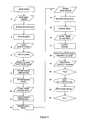
- FIG. 4illustrates one process of manufacturing a photodiode with back contacts as follows:
- Step 1forms a field oxide over the surface of a semiconductor substrate. This oxide acts as a masking layer during diffusion/implantation.
- Steps 2 through step 4form p+ regions on the back of the substrate which act as ohmic contact regions and channel stop regions.
- a diffusion process for boron dopingis described here, other doping techniques commonly used in the semiconductor industry such as ion implantation can also be used.
- Step 5 and step 6are photolithography and dry etch steps which form a channel in the substrate extending from the back of the photodiode to within 10 to 100 microns of the front surface.
- Step 7 through step 9form an n+ region around the channel created in steps 5 and 6 .
- n-type dopantWhen n-type dopant is introduced into the etched channel, it will diffuse radially and vertically into the substrate creating an electrical pathway from the front junction (to be formed) to the back contact.
- Steps 10 through step 12form an n+ region around the photodiode active area which acts as a guard ring that reduces the diode leakage current.
- Step 13 through step 15form the p+ region on the top surface of the photodiode which act as a channel stop.
- Step 16 and 17form an active area of the photodiode with shallow n-type doping in the p-substrate.
- Step 18forms a radiation hard oxide layer or metal silicide layer on the surface of the active area which acts as a passivating layer as well as an entrance window to radiation.
- Step 19 , 21 , and 22form electrical contacts on the back of the substrate.
- Step 20 and step 23verify that the desired electrical characteristics have been achieved.
- a photodiode with back contactscan be made from many different types of semiconductor materials including Si, GaN or SiC. Different processing techniques to form the photodiode with back contacts may be developed to achieve similar or better results as those presented here.
- FIG. 4 process flow chartdescribes the use of diffusion for doping, other semiconductor doping techniques like ion implantation can also be used to form the n- and p-type regions mentioned.
- a semiconductor photodiode having one electrical contact that extends from a p-n junction at the surface of the photodiode to the back of the photodiode substrate and the second contact formed on the back of the semiconductor substrateis provided and a process for manufacturing the invention is presented.
- This inventionwill provide the ability to place a photodiode extremely close to a surface. It will also provide a more durable device by eliminating the use of delicate wire bonds for electrical contacts.
- the manufacturing process presentedconsists of techniques that are well known in the semiconductor industry.
Landscapes
- Light Receiving Elements (AREA)
Abstract
Description
Not Applicable
Not Applicable
1. Field of Invention
This invention relates, in general, to semiconductor photodiodes, and more specifically to a semiconductor photodiode having one electrical contact that extends from a p-n junction at the surface of the photodiode to the back of the photodiode substrate and a second electrical contact located of the back of the photodiode substrate.
2. Description of Prior Art
A photodiode detector is broadly defined as a device that responds to incident electromagnetic radiation by converting the radiation into electrical energy, thereby enabling measurement of the intensity of the incident radiation. Usually, a photodiode structure requires a small wire to be bonded to the electrical contact on the top surface of the photodiode. This wire must extend above the photodiode surface and only touch the surface at the electrical contact point. These wires (normally referred to as wire bonds) are very delicate, prone to damage and limit the proximity that a photodiode can be to a surface. In some applications, such as x-ray, extreme ultraviolet and deep ultraviolet (XUV radiation) steppers, it is desirable to place the detector within a few micrometers to a given surface for dosimetry, imaging, position sensing and alignment applications. Wire bonds on the front surface of the photodiode, which typically are 1 millimeter high, will not allow this.
Photodiodes used as solar cells have been manufactured with electrical contacts on the back surface opposing the front active area (back contact devices) (citation #1). According to Smith et. al. (citation #2), there are three design categories of back contact cells, the Interdigitated Back-Contact (IBC) solar cell, the Emitter Wrap-Through (EWT) solar cell, and the contact wrap-through (CWT) solar cell.
Both the IBC solar cell and the CWT solar cell are not suitable designs for making a photodiode for XUV radiation detection. The IBC solar cell does not have an electrical contact that extends to the front surface of the diode which is needed for XUV photon detection. It is essential for XUV photodiodes to have the p-n junction formed near the surface as XUV radiation is absorbed within a fraction of a micron from the surface. The CWT solar cells have a metal grid on the cell surface which reduces the sensitivity of the cell. For many applications (mainly radiometric), it is desirable to have an XUV photodiode with very high sensitivity without any radiation absorbing structure on the active surface. Although the CWT solar cells have holes for front to back contact, the holes create an additional problem in realizing the XUV photodiodes as explained in the next paragraph. The buried contact EWT cell was one of the earliest versions developed. It uses laser drilled holes from front to back of the cell as well as laser cut channels for contact plating. The problem with this method is that the holes in the wafer will make it almost impossible to pattern wafers using photolithography techniques needed for the above mentioned applications. Several patterning steps are required to realize an XUV photodiode after formation of the front to back contact.
Fabrication of the back contact vertical junction solar cells have been described in U.S. Pat. No. 5,067,985 (citation # P1). Special (110) oriented silicon wafers were chosen and chemical etching was used to form a network of narrow channels into which impurities were diffused. Then a conducting material was deposited into the channels to form back contacts. (110) oriented silicon is useful only when long narrow channels are needed as in the solar cell structures. Small channel areas like those required in dense photodiode arrays can not be realized by wet chemical etching techniques.
We have made back contact photodiodes for x-ray steppers several years ago in which the holes in the wafer were formed by wet chemical etching through which the front contact was brought to the back of the photodiode. In this method, an area of about 0.75 mm×0.75 mm is needed to achieve the desired results. Hence, the photodiodes on the front of the wafer can not be placed closer than about a millimeter to each other, an undesirable feature when a photodiode dense array is desired for imaging purposes.
An obvious approach to avoid the use of wire bonds would be to mount the front surface of the diode onto a ceramic substrate and illuminate the diode from the back (citation #3). High XUV response of back illuminated devices dictates that the devices need to be thin so that the photogenerated carriers can diffuse to the front region. However, radiation hardness as that required by XUV photodiodes, has so far, not been demonstrated by the thin devices (citation #4).
A brute force approach used in some silicon controlled rectifier (thyristor) manufacturing processes, is to carry out the dopant diffusion in desired areas from the front and back of the wafer simultaneously. When the front and back diffusions meet, they form a conductive channel extending from the front of the device to the back of the device. However, temperatures in excess of 1200° C. and diffusion time in excess of a week are required to achieve the desired results. Such a high temperature and prolonged process time is known to mechanically deform the silicon wafers. If the wafers are deformed, it will be impossible to perform the submicron geometry patterning needed for the above XUV stepper applications.
Accordingly, it is an object of the present invention to provide a radiometric quality semiconductor photodiode with shallow p-n junction having one electrical contact through a small channel extending from the p-n junction to the back of the photodiode substrate and a second contact formed on the back of the semiconductor substrate. The electrical contact channel requires a cross sectional area of only 0.125 mm×0.125 mm with the present technology and can be made smaller as the semiconductor etching technology develops further.
Another object of the present invention is to provide a method of manufacturing a radiometric quality semiconductor photodiode with shallow p-n junction having one electrical contact through a small channel extending from the p-n junction to the back of the photodiode substrate and a second contact formed on the back of the semiconductor substrate. In the method proposed, the electrical contact channel will require a cross sectional area of only 0.125 mm×0.125 mm.
These and other objects and advantages are provided by a radiometric quality semiconductor photodiode with one electrical contact extending from a p-n junction at the photodiode surface to the back of the photodiode substrate and a second contact formed on the back of the semiconductor substrate. With the present technology, the electrical contact channel will require a cross sectional area of only 0.125 mm×0.125 mm.
This photodiode with back contacts will eliminate the need for delicate wire bonds which are prone to damage during handling and will also allow the photodiode to be placed extremely close to a surface. Because of the small contact channel area of 0.125 mm×0.125 mm, dense photodiode arrays can be manufactured.
A novel approach to accomplish this will require the formation of a channel by dry etching that will extend from back of the photodiode substrate to close to the p-n junction at the front of the photodiode. Impurities will then be diffused radially outward from the channel to provide an electrical pathway from the p-n junction to the back of the substrate. Dry etching will provide precise control of channel depth close to the photodiode front surface which would not be achievable with laser drilling as used in the prior art. This will provide a means for manufacturing a radiometric quality photodiode suitable for the previously mentioned applications.
According to one embodiment, the present invention comprises a radiometric quality semiconductor photodiode with shallow p-n junction having one electrical contact through a small channel extending from a p-n junction at the photodiode surface to the back of the photodiode substrate and a second contact formed on the back of the semiconductor substrate.
In another embodiment, the present invention comprises a method of making a radiometric quality semiconductor photodiode with shallow p-n junction having one electrical contact with a small channel extending from a p-n junction at the photodiode surface to the back of the photodiode substrate and a second contact formed on the back of the semiconductor substrate. The method comprises fabrication of a radiometric quality semiconductor photodiode having one electrical contact extending from a shallow p-n junction to the back of the photodiode substrate and with a second contact formed on the back of the semiconductor substrate by using techniques of photolithography and dry etching presently used in the semiconductor industry.
FIG. 1 illustrates the isometric view of one embodiment of the photodiode with back contacts.
FIG. 2 illustrates an enlarged subsection of the photodiode with back contacts.
FIG. 3 illustrates the cross section of the photodiode with back contacts.
FIG. 4 illustrates the process by which one embodiment of the photodiode with back contacts may be produced.
FIG. 1 (not to scale) illustrates an isometric view of a photodiode with back contacts. The photodiode can be fabricated by an ULSI (Ultra Large Scale Integrated Circuit) compatible process. Asubstrate 30 comprises a semiconductor material that is doped p-type. It should be understood that either n- or p-type conductivity can be used so long as junctions are formed with the proper dopant type as described herein below. Afield oxide layer 32 is located on the substrate. An n+guard ring region 34 and a p+channel stop region 36 are located on the substrate. A defect free n-typeactive region 38 is located on the front of the substrate. A passivating front window oxide layer ormetal silicide layer 40 is located on the substrate. Achannel 42 is etched into the back of the substrate extending to within 10 to 100 microns of the front surface. Ann+ region 44 is located in the substrate surrounding the etched channel and extending to the bottom of the substrate that will bring the front n-region to the back. A p+ohmic contact region 46 is located on the bottom of the substrate. Another p+channel stop region 48 is located on the back of the substrate. Gold forelectrical contacts 50 is located on the back of the substrate.
FIG. 2 (not to scale) shows an enlarged subsection of the photodiode with back contacts shown in FIG.1 and emphasizes the area in which the back contacts are formed.
FIG. 3 (not to scale) illustrates a cross section of the photodiode with back contacts shown in FIG.1.
FIG. 4 illustrates one process of manufacturing a photodiode with back contacts as follows:
A variety of modifications of the present invention will be obvious to those of ordinary skill in photodetector design and fabrication. A photodiode with back contacts can be made from many different types of semiconductor materials including Si, GaN or SiC. Different processing techniques to form the photodiode with back contacts may be developed to achieve similar or better results as those presented here. Although the FIG. 4 process flow chart describes the use of diffusion for doping, other semiconductor doping techniques like ion implantation can also be used to form the n- and p-type regions mentioned.
It should now be apparent that a semiconductor photodiode having one electrical contact that extends from a p-n junction at the surface of the photodiode to the back of the photodiode substrate and the second contact formed on the back of the semiconductor substrate is provided and a process for manufacturing the invention is presented. This invention will provide the ability to place a photodiode extremely close to a surface. It will also provide a more durable device by eliminating the use of delicate wire bonds for electrical contacts. The manufacturing process presented consists of techniques that are well known in the semiconductor industry.
Claims (2)
1. A semiconductor photodiode comprising a semiconductor substrate in which a p-n junction is formed and incident radiation energy can generate charge carriers separable by an electric field generated by said p-n junction and said carriers are conductible by first and second electrically conductive contacts,
where said first electrical contact extends from said p-n junction near the surface of said photodiode to the back of said photodiode substrate, and
said first electrical contact has an etched contact channel which extends from the back of said photodiode substrate to within 10 to 100 microns of said photodiode surface with cross sectional area of said channel having the dimensions of about 0.125 mm×0.125 mm, and
said second electrical contact is located on the back of said photodiode substrate.
2. A method for the fabrication of a semiconductor photodiode comprising a semiconductor substrate in which a p-n junction is formed and incident radiation energy can generate charge carriers separable by an electric field generated by said p-n junction and said carriers are conductible by first and second electrically conductive contacts, and
said first electrical contact extends from said p-n junction near the surface of said photodiode to the back of said photodiode substrate, and
said first electrical contact has an etched contact channel which extends from the back of said photodiode substrate to within 10 to 100 microns of said photodiode surface with cross sectional area of said channel having the dimensions of about 0.125 mm×0.125 mm and is created by a combination of masking, dry etching and diffusion, and
said second electrical contact is located on the back of said substrate of said photodiode and is created by standard photolithography and doping techniques.
Priority Applications (1)
| Application Number | Priority Date | Filing Date | Title |
|---|---|---|---|
| US10/254,369US6777729B1 (en) | 2002-09-25 | 2002-09-25 | Semiconductor photodiode with back contacts |
Applications Claiming Priority (1)
| Application Number | Priority Date | Filing Date | Title |
|---|---|---|---|
| US10/254,369US6777729B1 (en) | 2002-09-25 | 2002-09-25 | Semiconductor photodiode with back contacts |
Publications (1)
| Publication Number | Publication Date |
|---|---|
| US6777729B1true US6777729B1 (en) | 2004-08-17 |
Family
ID=32849413
Family Applications (1)
| Application Number | Title | Priority Date | Filing Date |
|---|---|---|---|
| US10/254,369Expired - LifetimeUS6777729B1 (en) | 2002-09-25 | 2002-09-25 | Semiconductor photodiode with back contacts |
Country Status (1)
| Country | Link |
|---|---|
| US (1) | US6777729B1 (en) |
Cited By (18)
| Publication number | Priority date | Publication date | Assignee | Title |
|---|---|---|---|---|
| US20040261840A1 (en)* | 2003-06-30 | 2004-12-30 | Advent Solar, Inc. | Emitter wrap-through back contact solar cells on thin silicon wafers |
| US20050172998A1 (en)* | 2004-02-05 | 2005-08-11 | Advent Solar, Inc. | Buried-contact solar cells with self-doping contacts |
| US20050172996A1 (en)* | 2004-02-05 | 2005-08-11 | Advent Solar, Inc. | Contact fabrication of emitter wrap-through back contact silicon solar cells |
| US20050176164A1 (en)* | 2004-02-05 | 2005-08-11 | Advent Solar, Inc. | Back-contact solar cells and methods for fabrication |
| US20050221541A1 (en)* | 2003-06-25 | 2005-10-06 | Metzler Richard A | Ultra thin back-illuminated photodiode array fabrication methods |
| US20060060238A1 (en)* | 2004-02-05 | 2006-03-23 | Advent Solar, Inc. | Process and fabrication methods for emitter wrap through back contact solar cells |
| US20060162766A1 (en)* | 2003-06-26 | 2006-07-27 | Advent Solar, Inc. | Back-contacted solar cells with integral conductive vias and method of making |
| WO2006117980A1 (en) | 2005-04-26 | 2006-11-09 | Shin-Etsu Handotai Co., Ltd. | Solar cell manufacturing method, solar cell, and semiconductor device manufacturing method |
| US20070158708A1 (en)* | 2003-03-10 | 2007-07-12 | Hamamatsu Photonics K.K. | Photodiode array, method for manufacturing same, and radiation detector |
| US20080143601A1 (en)* | 2006-11-30 | 2008-06-19 | Tenxc Wireless Inc. | Butler matrix implementation |
| US20080216887A1 (en)* | 2006-12-22 | 2008-09-11 | Advent Solar, Inc. | Interconnect Technologies for Back Contact Solar Cells and Modules |
| US20080315121A1 (en)* | 2007-06-25 | 2008-12-25 | Asml Netherlands B.V. | Radiation detector, method of manufacturing a radiation detector and lithographic apparatus comprising a radiation detector |
| US20090021717A1 (en)* | 2007-06-25 | 2009-01-22 | Asml Netherlands B.V. | Radiation Detector, Method of Manufacturing a Radiation Detector, and Lithographic Apparatus Comprising a Radiation Detector |
| US20090126786A1 (en)* | 2007-11-13 | 2009-05-21 | Advent Solar, Inc. | Selective Emitter and Texture Processes for Back Contact Solar Cells |
| US7576371B1 (en)* | 2006-03-03 | 2009-08-18 | Array Optronix, Inc. | Structures and methods to improve the crosstalk between adjacent pixels of back-illuminated photodiode arrays |
| US20100012172A1 (en)* | 2008-04-29 | 2010-01-21 | Advent Solar, Inc. | Photovoltaic Modules Manufactured Using Monolithic Module Assembly Techniques |
| US20100181634A1 (en)* | 2009-01-21 | 2010-07-22 | Taiwan Semiconductor Manufacturing Company, Ltd. | Method and structure for reducing cross-talk in image sensor devices |
| US20120275480A1 (en)* | 2011-04-26 | 2012-11-01 | Hidetoshi Koike | Solid-state imaging device and manufacturing method thereof |
Citations (3)
| Publication number | Priority date | Publication date | Assignee | Title |
|---|---|---|---|---|
| US5067985A (en) | 1990-06-08 | 1991-11-26 | The United States Of America As Represented By The Secretary Of The Air Force | Back-contact vertical-junction solar cell and method |
| US6066510A (en)* | 1996-10-21 | 2000-05-23 | Foveon, Inc. | Method for forming a photodiode with improved photoresponse behavior |
| US20030054585A1 (en)* | 2001-09-17 | 2003-03-20 | Keiji Mabuchi | Solid-state imaging device and method for manufacturing same |
- 2002
- 2002-09-25USUS10/254,369patent/US6777729B1/ennot_activeExpired - Lifetime
Patent Citations (3)
| Publication number | Priority date | Publication date | Assignee | Title |
|---|---|---|---|---|
| US5067985A (en) | 1990-06-08 | 1991-11-26 | The United States Of America As Represented By The Secretary Of The Air Force | Back-contact vertical-junction solar cell and method |
| US6066510A (en)* | 1996-10-21 | 2000-05-23 | Foveon, Inc. | Method for forming a photodiode with improved photoresponse behavior |
| US20030054585A1 (en)* | 2001-09-17 | 2003-03-20 | Keiji Mabuchi | Solid-state imaging device and method for manufacturing same |
Cited By (34)
| Publication number | Priority date | Publication date | Assignee | Title |
|---|---|---|---|---|
| US20070158708A1 (en)* | 2003-03-10 | 2007-07-12 | Hamamatsu Photonics K.K. | Photodiode array, method for manufacturing same, and radiation detector |
| US7462553B2 (en) | 2003-06-25 | 2008-12-09 | Semicoa | Ultra thin back-illuminated photodiode array fabrication methods |
| US20050221541A1 (en)* | 2003-06-25 | 2005-10-06 | Metzler Richard A | Ultra thin back-illuminated photodiode array fabrication methods |
| US20060162766A1 (en)* | 2003-06-26 | 2006-07-27 | Advent Solar, Inc. | Back-contacted solar cells with integral conductive vias and method of making |
| US20040261840A1 (en)* | 2003-06-30 | 2004-12-30 | Advent Solar, Inc. | Emitter wrap-through back contact solar cells on thin silicon wafers |
| US7649141B2 (en) | 2003-06-30 | 2010-01-19 | Advent Solar, Inc. | Emitter wrap-through back contact solar cells on thin silicon wafers |
| US7335555B2 (en) | 2004-02-05 | 2008-02-26 | Advent Solar, Inc. | Buried-contact solar cells with self-doping contacts |
| US20050172996A1 (en)* | 2004-02-05 | 2005-08-11 | Advent Solar, Inc. | Contact fabrication of emitter wrap-through back contact silicon solar cells |
| US7144751B2 (en) | 2004-02-05 | 2006-12-05 | Advent Solar, Inc. | Back-contact solar cells and methods for fabrication |
| US20060060238A1 (en)* | 2004-02-05 | 2006-03-23 | Advent Solar, Inc. | Process and fabrication methods for emitter wrap through back contact solar cells |
| US20050176164A1 (en)* | 2004-02-05 | 2005-08-11 | Advent Solar, Inc. | Back-contact solar cells and methods for fabrication |
| US20090320922A1 (en)* | 2004-02-05 | 2009-12-31 | Advent Solar, Inc. | Contact Fabrication of Emitter Wrap-Through Back Contact Silicon Solar Cells |
| US7863084B2 (en) | 2004-02-05 | 2011-01-04 | Applied Materials, Inc | Contact fabrication of emitter wrap-through back contact silicon solar cells |
| US20050172998A1 (en)* | 2004-02-05 | 2005-08-11 | Advent Solar, Inc. | Buried-contact solar cells with self-doping contacts |
| EP1876651A4 (en)* | 2005-04-26 | 2013-09-11 | Shinetsu Handotai Kk | SOLAR CELL MANUFACTURING METHOD, SOLAR CELL AND METHOD FOR PRODUCING SEMICONDUCTOR COMPONENTS |
| US20090020158A1 (en)* | 2005-04-26 | 2009-01-22 | Shin-Etsu Handotai Co., Ltd. | Method for manufacturing solar cell and solar cell, and method for manufacturing semiconductor device |
| WO2006117980A1 (en) | 2005-04-26 | 2006-11-09 | Shin-Etsu Handotai Co., Ltd. | Solar cell manufacturing method, solar cell, and semiconductor device manufacturing method |
| US7875890B1 (en) | 2006-03-03 | 2011-01-25 | Array Optronix, Inc. | Structures and methods to improve the crosstalk between adjacent pixels of back-illuminated photodiode arrays |
| US7576371B1 (en)* | 2006-03-03 | 2009-08-18 | Array Optronix, Inc. | Structures and methods to improve the crosstalk between adjacent pixels of back-illuminated photodiode arrays |
| US20080143601A1 (en)* | 2006-11-30 | 2008-06-19 | Tenxc Wireless Inc. | Butler matrix implementation |
| US20080216887A1 (en)* | 2006-12-22 | 2008-09-11 | Advent Solar, Inc. | Interconnect Technologies for Back Contact Solar Cells and Modules |
| US20090021717A1 (en)* | 2007-06-25 | 2009-01-22 | Asml Netherlands B.V. | Radiation Detector, Method of Manufacturing a Radiation Detector, and Lithographic Apparatus Comprising a Radiation Detector |
| US7586108B2 (en)* | 2007-06-25 | 2009-09-08 | Asml Netherlands B.V. | Radiation detector, method of manufacturing a radiation detector and lithographic apparatus comprising a radiation detector |
| US8138485B2 (en)* | 2007-06-25 | 2012-03-20 | Asml Netherlands B.V. | Radiation detector, method of manufacturing a radiation detector, and lithographic apparatus comprising a radiation detector |
| US8426831B2 (en) | 2007-06-25 | 2013-04-23 | Asml Netherlands B.V. | Radiation detector, method of manufacturing a radiation detector, and lithographic apparatus comprising a radiation detector |
| US20080315121A1 (en)* | 2007-06-25 | 2008-12-25 | Asml Netherlands B.V. | Radiation detector, method of manufacturing a radiation detector and lithographic apparatus comprising a radiation detector |
| US20090126786A1 (en)* | 2007-11-13 | 2009-05-21 | Advent Solar, Inc. | Selective Emitter and Texture Processes for Back Contact Solar Cells |
| US20100012172A1 (en)* | 2008-04-29 | 2010-01-21 | Advent Solar, Inc. | Photovoltaic Modules Manufactured Using Monolithic Module Assembly Techniques |
| US20110067751A1 (en)* | 2008-04-29 | 2011-03-24 | Meakin David H | Photovoltaic modules manufactured using monolithic module assembly techniques |
| US20100181634A1 (en)* | 2009-01-21 | 2010-07-22 | Taiwan Semiconductor Manufacturing Company, Ltd. | Method and structure for reducing cross-talk in image sensor devices |
| US7824948B2 (en)* | 2009-01-21 | 2010-11-02 | Taiwan Semiconductor Manufacturing Company, Ltd. | Method and structure for reducing cross-talk in image sensor devices |
| CN101783318B (en)* | 2009-01-21 | 2012-01-25 | 台湾积体电路制造股份有限公司 | Method and structure for reducing cross-talk in image sensor devices |
| US20120275480A1 (en)* | 2011-04-26 | 2012-11-01 | Hidetoshi Koike | Solid-state imaging device and manufacturing method thereof |
| US8659060B2 (en)* | 2011-04-26 | 2014-02-25 | Kabushiki Kaisha Toshiba | Solid-state imaging device and manufacturing method thereof |
Similar Documents
| Publication | Publication Date | Title |
|---|---|---|
| US6777729B1 (en) | Semiconductor photodiode with back contacts | |
| US9236519B2 (en) | Geiger-mode avalanche photodiode with high signal-to-noise ratio, and corresponding manufacturing process | |
| US4127932A (en) | Method of fabricating silicon photodiodes | |
| US4070689A (en) | Semiconductor solar energy device | |
| JP4278515B2 (en) | Solar cell and solar cell manufacturing method | |
| KR101889429B1 (en) | Bypass Diode for a Solar Cell | |
| EP0625803B1 (en) | Photodiode structure | |
| US9214588B2 (en) | Wavelength sensitive sensor photodiodes | |
| CN111223960B (en) | Method for manufacturing at least one passivated planar photodiode with reduced dark current | |
| EP0616373A2 (en) | Photoelectric conversion semiconductor device and method of manufacturing the same | |
| US3529217A (en) | Photosensitive semiconductor device | |
| US5994751A (en) | Photodiode having reduced series resistance, and method for fabrication thereof | |
| CN102187469A (en) | Electromagnetic radiation converter and battery | |
| KR20070104422A (en) | Photosensitive device having increased blue light sensitivity, manufacturing method and operating method thereof | |
| JPH0346279A (en) | Hetero junction photodiode | |
| CN110212044A (en) | A kind of deep trouth semiconductor light detecting structure and its manufacturing method | |
| US6621064B2 (en) | CMOS photodiode having reduced dark current and improved light sensitivity and responsivity | |
| US5854506A (en) | Semiconductor particle-detector | |
| US4219830A (en) | Semiconductor solar cell | |
| US4742017A (en) | Implantation method for forming Schottky barrier photodiodes | |
| CA1078948A (en) | Method of fabricating silicon photodiodes | |
| US4751560A (en) | Infrared photodiode array | |
| KR100709645B1 (en) | Radiation hardened visible p-i-n detector | |
| KR101768704B1 (en) | photo multiplier and manufacturing method for the same | |
| JPS5914180B2 (en) | photodetector cell |
Legal Events
| Date | Code | Title | Description |
|---|---|---|---|
| AS | Assignment | Owner name:INTERNATIONAL RADIATION DETECTORS INC., CALIFORNIA Free format text:ASSIGNMENT OF ASSIGNORS INTEREST;ASSIGNOR:PRINCE, CHAD;REEL/FRAME:014198/0055 Effective date:20030613 | |
| STCF | Information on status: patent grant | Free format text:PATENTED CASE | |
| REMI | Maintenance fee reminder mailed | ||
| FPAY | Fee payment | Year of fee payment:4 | |
| SULP | Surcharge for late payment | ||
| AS | Assignment | Owner name:ILLINOIS TOOL WORKS INC., ILLINOIS Free format text:ASSIGNMENT OF ASSIGNORS INTEREST;ASSIGNOR:INTERNATIONAL RADIATION DETECTORS, INC.;REEL/FRAME:025952/0863 Effective date:20101223 | |
| FPAY | Fee payment | Year of fee payment:8 | |
| SULP | Surcharge for late payment | ||
| FEPP | Fee payment procedure | Free format text:PAT HOLDER NO LONGER CLAIMS SMALL ENTITY STATUS, ENTITY STATUS SET TO UNDISCOUNTED (ORIGINAL EVENT CODE: STOL); ENTITY STATUS OF PATENT OWNER: LARGE ENTITY | |
| FPAY | Fee payment | Year of fee payment:12 |