US6777712B2 - Low-power organic light emitting diode pixel circuit - Google Patents
Low-power organic light emitting diode pixel circuitDownload PDFInfo
- Publication number
- US6777712B2 US6777712B2US10/390,809US39080903AUS6777712B2US 6777712 B2US6777712 B2US 6777712B2US 39080903 AUS39080903 AUS 39080903AUS 6777712 B2US6777712 B2US 6777712B2
- Authority
- US
- United States
- Prior art keywords
- oled
- circuit
- pixel circuit
- pixel
- voltage
- Prior art date
- Legal status (The legal status is an assumption and is not a legal conclusion. Google has not performed a legal analysis and makes no representation as to the accuracy of the status listed.)
- Expired - Lifetime
Links
Images


Classifications
- G—PHYSICS
- G09—EDUCATION; CRYPTOGRAPHY; DISPLAY; ADVERTISING; SEALS
- G09G—ARRANGEMENTS OR CIRCUITS FOR CONTROL OF INDICATING DEVICES USING STATIC MEANS TO PRESENT VARIABLE INFORMATION
- G09G3/00—Control arrangements or circuits, of interest only in connection with visual indicators other than cathode-ray tubes
- G09G3/20—Control arrangements or circuits, of interest only in connection with visual indicators other than cathode-ray tubes for presentation of an assembly of a number of characters, e.g. a page, by composing the assembly by combination of individual elements arranged in a matrix no fixed position being assigned to or needed to be assigned to the individual characters or partial characters
- G09G3/22—Control arrangements or circuits, of interest only in connection with visual indicators other than cathode-ray tubes for presentation of an assembly of a number of characters, e.g. a page, by composing the assembly by combination of individual elements arranged in a matrix no fixed position being assigned to or needed to be assigned to the individual characters or partial characters using controlled light sources
- G09G3/30—Control arrangements or circuits, of interest only in connection with visual indicators other than cathode-ray tubes for presentation of an assembly of a number of characters, e.g. a page, by composing the assembly by combination of individual elements arranged in a matrix no fixed position being assigned to or needed to be assigned to the individual characters or partial characters using controlled light sources using electroluminescent panels
- G09G3/32—Control arrangements or circuits, of interest only in connection with visual indicators other than cathode-ray tubes for presentation of an assembly of a number of characters, e.g. a page, by composing the assembly by combination of individual elements arranged in a matrix no fixed position being assigned to or needed to be assigned to the individual characters or partial characters using controlled light sources using electroluminescent panels semiconductive, e.g. using light-emitting diodes [LED]
- G09G3/3208—Control arrangements or circuits, of interest only in connection with visual indicators other than cathode-ray tubes for presentation of an assembly of a number of characters, e.g. a page, by composing the assembly by combination of individual elements arranged in a matrix no fixed position being assigned to or needed to be assigned to the individual characters or partial characters using controlled light sources using electroluminescent panels semiconductive, e.g. using light-emitting diodes [LED] organic, e.g. using organic light-emitting diodes [OLED]
- G09G3/3225—Control arrangements or circuits, of interest only in connection with visual indicators other than cathode-ray tubes for presentation of an assembly of a number of characters, e.g. a page, by composing the assembly by combination of individual elements arranged in a matrix no fixed position being assigned to or needed to be assigned to the individual characters or partial characters using controlled light sources using electroluminescent panels semiconductive, e.g. using light-emitting diodes [LED] organic, e.g. using organic light-emitting diodes [OLED] using an active matrix
- G09G3/3233—Control arrangements or circuits, of interest only in connection with visual indicators other than cathode-ray tubes for presentation of an assembly of a number of characters, e.g. a page, by composing the assembly by combination of individual elements arranged in a matrix no fixed position being assigned to or needed to be assigned to the individual characters or partial characters using controlled light sources using electroluminescent panels semiconductive, e.g. using light-emitting diodes [LED] organic, e.g. using organic light-emitting diodes [OLED] using an active matrix with pixel circuitry controlling the current through the light-emitting element
- G—PHYSICS
- G09—EDUCATION; CRYPTOGRAPHY; DISPLAY; ADVERTISING; SEALS
- G09G—ARRANGEMENTS OR CIRCUITS FOR CONTROL OF INDICATING DEVICES USING STATIC MEANS TO PRESENT VARIABLE INFORMATION
- G09G3/00—Control arrangements or circuits, of interest only in connection with visual indicators other than cathode-ray tubes
- G09G3/20—Control arrangements or circuits, of interest only in connection with visual indicators other than cathode-ray tubes for presentation of an assembly of a number of characters, e.g. a page, by composing the assembly by combination of individual elements arranged in a matrix no fixed position being assigned to or needed to be assigned to the individual characters or partial characters
- G09G3/22—Control arrangements or circuits, of interest only in connection with visual indicators other than cathode-ray tubes for presentation of an assembly of a number of characters, e.g. a page, by composing the assembly by combination of individual elements arranged in a matrix no fixed position being assigned to or needed to be assigned to the individual characters or partial characters using controlled light sources
- G09G3/30—Control arrangements or circuits, of interest only in connection with visual indicators other than cathode-ray tubes for presentation of an assembly of a number of characters, e.g. a page, by composing the assembly by combination of individual elements arranged in a matrix no fixed position being assigned to or needed to be assigned to the individual characters or partial characters using controlled light sources using electroluminescent panels
- G—PHYSICS
- G09—EDUCATION; CRYPTOGRAPHY; DISPLAY; ADVERTISING; SEALS
- G09G—ARRANGEMENTS OR CIRCUITS FOR CONTROL OF INDICATING DEVICES USING STATIC MEANS TO PRESENT VARIABLE INFORMATION
- G09G3/00—Control arrangements or circuits, of interest only in connection with visual indicators other than cathode-ray tubes
- G09G3/20—Control arrangements or circuits, of interest only in connection with visual indicators other than cathode-ray tubes for presentation of an assembly of a number of characters, e.g. a page, by composing the assembly by combination of individual elements arranged in a matrix no fixed position being assigned to or needed to be assigned to the individual characters or partial characters
- G09G3/2007—Display of intermediate tones
- G09G3/2014—Display of intermediate tones by modulation of the duration of a single pulse during which the logic level remains constant
- G—PHYSICS
- G11—INFORMATION STORAGE
- G11C—STATIC STORES
- G11C11/00—Digital stores characterised by the use of particular electric or magnetic storage elements; Storage elements therefor
- G11C11/21—Digital stores characterised by the use of particular electric or magnetic storage elements; Storage elements therefor using electric elements
- G11C11/34—Digital stores characterised by the use of particular electric or magnetic storage elements; Storage elements therefor using electric elements using semiconductor devices
- G11C11/40—Digital stores characterised by the use of particular electric or magnetic storage elements; Storage elements therefor using electric elements using semiconductor devices using transistors
- G11C11/41—Digital stores characterised by the use of particular electric or magnetic storage elements; Storage elements therefor using electric elements using semiconductor devices using transistors forming static cells with positive feedback, i.e. cells not needing refreshing or charge regeneration, e.g. bistable multivibrator or Schmitt trigger
- G11C11/413—Auxiliary circuits, e.g. for addressing, decoding, driving, writing, sensing, timing or power reduction
- G11C11/417—Auxiliary circuits, e.g. for addressing, decoding, driving, writing, sensing, timing or power reduction for memory cells of the field-effect type
- G11C11/419—Read-write [R-W] circuits
- G—PHYSICS
- G09—EDUCATION; CRYPTOGRAPHY; DISPLAY; ADVERTISING; SEALS
- G09G—ARRANGEMENTS OR CIRCUITS FOR CONTROL OF INDICATING DEVICES USING STATIC MEANS TO PRESENT VARIABLE INFORMATION
- G09G2300/00—Aspects of the constitution of display devices
- G09G2300/08—Active matrix structure, i.e. with use of active elements, inclusive of non-linear two terminal elements, in the pixels together with light emitting or modulating elements
- G09G2300/0809—Several active elements per pixel in active matrix panels
- G09G2300/0842—Several active elements per pixel in active matrix panels forming a memory circuit, e.g. a dynamic memory with one capacitor
- G09G2300/0857—Static memory circuit, e.g. flip-flop
- G—PHYSICS
- G09—EDUCATION; CRYPTOGRAPHY; DISPLAY; ADVERTISING; SEALS
- G09G—ARRANGEMENTS OR CIRCUITS FOR CONTROL OF INDICATING DEVICES USING STATIC MEANS TO PRESENT VARIABLE INFORMATION
- G09G2300/00—Aspects of the constitution of display devices
- G09G2300/08—Active matrix structure, i.e. with use of active elements, inclusive of non-linear two terminal elements, in the pixels together with light emitting or modulating elements
- G09G2300/0809—Several active elements per pixel in active matrix panels
- G09G2300/0842—Several active elements per pixel in active matrix panels forming a memory circuit, e.g. a dynamic memory with one capacitor
- G09G2300/0861—Several active elements per pixel in active matrix panels forming a memory circuit, e.g. a dynamic memory with one capacitor with additional control of the display period without amending the charge stored in a pixel memory, e.g. by means of additional select electrodes
- G—PHYSICS
- G09—EDUCATION; CRYPTOGRAPHY; DISPLAY; ADVERTISING; SEALS
- G09G—ARRANGEMENTS OR CIRCUITS FOR CONTROL OF INDICATING DEVICES USING STATIC MEANS TO PRESENT VARIABLE INFORMATION
- G09G2310/00—Command of the display device
- G09G2310/02—Addressing, scanning or driving the display screen or processing steps related thereto
- G09G2310/0243—Details of the generation of driving signals
- G09G2310/0254—Control of polarity reversal in general, other than for liquid crystal displays
- G09G2310/0256—Control of polarity reversal in general, other than for liquid crystal displays with the purpose of reversing the voltage across a light emitting or modulating element within a pixel
- G—PHYSICS
- G09—EDUCATION; CRYPTOGRAPHY; DISPLAY; ADVERTISING; SEALS
- G09G—ARRANGEMENTS OR CIRCUITS FOR CONTROL OF INDICATING DEVICES USING STATIC MEANS TO PRESENT VARIABLE INFORMATION
- G09G2310/00—Command of the display device
- G09G2310/06—Details of flat display driving waveforms
- G09G2310/061—Details of flat display driving waveforms for resetting or blanking
- G09G2310/063—Waveforms for resetting the whole screen at once
- G—PHYSICS
- G09—EDUCATION; CRYPTOGRAPHY; DISPLAY; ADVERTISING; SEALS
- G09G—ARRANGEMENTS OR CIRCUITS FOR CONTROL OF INDICATING DEVICES USING STATIC MEANS TO PRESENT VARIABLE INFORMATION
- G09G2320/00—Control of display operating conditions
- G09G2320/02—Improving the quality of display appearance
- G09G2320/0233—Improving the luminance or brightness uniformity across the screen
- G—PHYSICS
- G09—EDUCATION; CRYPTOGRAPHY; DISPLAY; ADVERTISING; SEALS
- G09G—ARRANGEMENTS OR CIRCUITS FOR CONTROL OF INDICATING DEVICES USING STATIC MEANS TO PRESENT VARIABLE INFORMATION
- G09G2320/00—Control of display operating conditions
- G09G2320/04—Maintaining the quality of display appearance
- G09G2320/043—Preventing or counteracting the effects of ageing
- G09G2320/046—Dealing with screen burn-in prevention or compensation of the effects thereof
- G—PHYSICS
- G09—EDUCATION; CRYPTOGRAPHY; DISPLAY; ADVERTISING; SEALS
- G09G—ARRANGEMENTS OR CIRCUITS FOR CONTROL OF INDICATING DEVICES USING STATIC MEANS TO PRESENT VARIABLE INFORMATION
- G09G2320/00—Control of display operating conditions
- G09G2320/06—Adjustment of display parameters
- G09G2320/0626—Adjustment of display parameters for control of overall brightness
- G09G2320/0633—Adjustment of display parameters for control of overall brightness by amplitude modulation of the brightness of the illumination source
- G—PHYSICS
- G09—EDUCATION; CRYPTOGRAPHY; DISPLAY; ADVERTISING; SEALS
- G09G—ARRANGEMENTS OR CIRCUITS FOR CONTROL OF INDICATING DEVICES USING STATIC MEANS TO PRESENT VARIABLE INFORMATION
- G09G2320/00—Control of display operating conditions
- G09G2320/06—Adjustment of display parameters
- G09G2320/0626—Adjustment of display parameters for control of overall brightness
- G09G2320/064—Adjustment of display parameters for control of overall brightness by time modulation of the brightness of the illumination source
- G—PHYSICS
- G09—EDUCATION; CRYPTOGRAPHY; DISPLAY; ADVERTISING; SEALS
- G09G—ARRANGEMENTS OR CIRCUITS FOR CONTROL OF INDICATING DEVICES USING STATIC MEANS TO PRESENT VARIABLE INFORMATION
- G09G2330/00—Aspects of power supply; Aspects of display protection and defect management
- G09G2330/02—Details of power systems and of start or stop of display operation
- G09G2330/021—Power management, e.g. power saving
- G09G2330/022—Power management, e.g. power saving in absence of operation, e.g. no data being entered during a predetermined time
- G—PHYSICS
- G09—EDUCATION; CRYPTOGRAPHY; DISPLAY; ADVERTISING; SEALS
- G09G—ARRANGEMENTS OR CIRCUITS FOR CONTROL OF INDICATING DEVICES USING STATIC MEANS TO PRESENT VARIABLE INFORMATION
- G09G2330/00—Aspects of power supply; Aspects of display protection and defect management
- G09G2330/04—Display protection
- G—PHYSICS
- G09—EDUCATION; CRYPTOGRAPHY; DISPLAY; ADVERTISING; SEALS
- G09G—ARRANGEMENTS OR CIRCUITS FOR CONTROL OF INDICATING DEVICES USING STATIC MEANS TO PRESENT VARIABLE INFORMATION
- G09G3/00—Control arrangements or circuits, of interest only in connection with visual indicators other than cathode-ray tubes
- G09G3/006—Electronic inspection or testing of displays and display drivers, e.g. of LED or LCD displays
- G—PHYSICS
- G09—EDUCATION; CRYPTOGRAPHY; DISPLAY; ADVERTISING; SEALS
- G09G—ARRANGEMENTS OR CIRCUITS FOR CONTROL OF INDICATING DEVICES USING STATIC MEANS TO PRESENT VARIABLE INFORMATION
- G09G3/00—Control arrangements or circuits, of interest only in connection with visual indicators other than cathode-ray tubes
- G09G3/20—Control arrangements or circuits, of interest only in connection with visual indicators other than cathode-ray tubes for presentation of an assembly of a number of characters, e.g. a page, by composing the assembly by combination of individual elements arranged in a matrix no fixed position being assigned to or needed to be assigned to the individual characters or partial characters
- G09G3/22—Control arrangements or circuits, of interest only in connection with visual indicators other than cathode-ray tubes for presentation of an assembly of a number of characters, e.g. a page, by composing the assembly by combination of individual elements arranged in a matrix no fixed position being assigned to or needed to be assigned to the individual characters or partial characters using controlled light sources
- G09G3/30—Control arrangements or circuits, of interest only in connection with visual indicators other than cathode-ray tubes for presentation of an assembly of a number of characters, e.g. a page, by composing the assembly by combination of individual elements arranged in a matrix no fixed position being assigned to or needed to be assigned to the individual characters or partial characters using controlled light sources using electroluminescent panels
- G09G3/32—Control arrangements or circuits, of interest only in connection with visual indicators other than cathode-ray tubes for presentation of an assembly of a number of characters, e.g. a page, by composing the assembly by combination of individual elements arranged in a matrix no fixed position being assigned to or needed to be assigned to the individual characters or partial characters using controlled light sources using electroluminescent panels semiconductive, e.g. using light-emitting diodes [LED]
- G09G3/3208—Control arrangements or circuits, of interest only in connection with visual indicators other than cathode-ray tubes for presentation of an assembly of a number of characters, e.g. a page, by composing the assembly by combination of individual elements arranged in a matrix no fixed position being assigned to or needed to be assigned to the individual characters or partial characters using controlled light sources using electroluminescent panels semiconductive, e.g. using light-emitting diodes [LED] organic, e.g. using organic light-emitting diodes [OLED]
- G09G3/3275—Details of drivers for data electrodes
- G09G3/3291—Details of drivers for data electrodes in which the data driver supplies a variable data voltage for setting the current through, or the voltage across, the light-emitting elements
- H—ELECTRICITY
- H10—SEMICONDUCTOR DEVICES; ELECTRIC SOLID-STATE DEVICES NOT OTHERWISE PROVIDED FOR
- H10K—ORGANIC ELECTRIC SOLID-STATE DEVICES
- H10K59/00—Integrated devices, or assemblies of multiple devices, comprising at least one organic light-emitting element covered by group H10K50/00
- H—ELECTRICITY
- H10—SEMICONDUCTOR DEVICES; ELECTRIC SOLID-STATE DEVICES NOT OTHERWISE PROVIDED FOR
- H10K—ORGANIC ELECTRIC SOLID-STATE DEVICES
- H10K59/00—Integrated devices, or assemblies of multiple devices, comprising at least one organic light-emitting element covered by group H10K50/00
- H10K59/10—OLED displays
- H10K59/12—Active-matrix OLED [AMOLED] displays
Definitions
- This inventionrelates generally to a pixel circuit, and, more particularly, to a low-power organic light emitting diode (OLED) pixel circuit utilizing complementary metal oxide semiconductor (CMOS) technology.
- OLEDorganic light emitting diode
- CMOScomplementary metal oxide semiconductor
- An OLED pixelmay utilize any of a variety of organic materials that emit light when an electric current is applied thereto.
- An OLED displaycomprises a plurality of OLED pixels organized into an array.
- Illumination of an OLED pixelis controlled by a pixel circuit that may include either a constant current source or a constant voltage source. It is generally recognized that the constant current source provides a greater uniformity of luminance among the pixels of the array. This is because the dependence of luminance upon current tends to be uniform while the voltage across the OLEDs at a given current in the various pixels tends to be less uniform.
- U.S. Pat. No. 6,023,259 to Howard et al.describes a current driver that provides a passive matrix drive current to an OLED. For typical display brightness, passive matrix drive operation results in lower OLED power efficiency and, in order to avoid flicker, requires a refresh rate greater than or equal to 60 Hz.
- a disadvantage of such an arrangementis that the voltage quickly bleeds off the capacitors, and consequently any image represented on the display must be regularly refreshed. This act of refreshing the image consumes a significant quantity of power. It is therefore desirable to find an alternative to the conventional use of dynamic RAMs.
- Control of the luminance of an “on” pixelis commonly achieved by controlling a magnitude of an analog voltage that determines the voltage or current applied to the pixel.
- Analog control circuitsare another source of excessive power dissipation. It is therefore desirable to find an alternative to the conventional use of analog control circuitry.
- the OLED displayis constructed of thin layers of organic material in which individual OLED pixels are subject to an occasional short circuit between an anode of the OLED and a counter-electrode of the OLED. Such a short can cause excess current to flow in the circuit, excess voltage across the pixel circuit and excess power dissipation. Good pixels neighboring a shorted pixel may be destroyed by heat from the shorted pixel and the excess current may alter power supply voltages.
- the layers of organic materialtend to trap charge, causing increases in the voltage drop across the OLED, which can cause a non-uniformity of luminance and a burned-in image.
- the trapped chargemay be removed by reverse-biasing the OLED.
- CMOScomplementary metal-oxide-semiconductor
- OLEDitself typically requires a voltage on the order of +/ ⁇ 6 volts to develop an adequate luminance when turned ON and to remove trapped charge when reverse-biased.
- Conventional CMOS integrated circuit technologyuses transistors that operate with a voltage of less than 4 volts. Accordingly, CMOS technology is not ordinarily capable of driving an OLED.
- a CMOS device in an OLED pixel circuitis particularly susceptible to damage from the voltage in excess of 4 volts.
- a traditional manner of changing a displayed imageis for a processor to update the memory of a display controller that periodically and individually addresses each of the pixels of the display, and turn them “on” (ON) and “off” (OFF) as required. If the display included a large number of pixels, for example one hundred thousand, one million, or more, this operation would consume a significant quantity of power and could burden the processor.
- An additional problem when incorporating a plurality of pixel circuits into a displayis that of physically distributing the collective elements of the display. That is, the display is a finite area within which the pixels and their accompanying circuitry are confined, yet a constant pitch between pixels must be maintained in order to provide a uniform image.
- OLED displayshave not been as readily adopted by designers as have many other conventional display technologies.
- the use of dynamic RAM and its corresponding circuitry required for refreshing an image, and issues relating to power dissipationare an obstacle to an employment of OLEDs in battery operated devices, and in small displays such as those used for hand-held devices or watches.
- the OLED operating voltagesare an obstacle to the use of CMOS circuitry in an OLED pixel circuit.
- the regular addressing of every pixel in an arrayis an obstacle to the employment of OLEDs in large displays.
- the maintenance of a constant pitch between pixelsis an important consideration in any display.
- a pixel circuitincludes an organic light emitting diode (OLED), and a static memory for storing data that represents an operational state of the OLED.
- OLEDorganic light emitting diode
- a pixel circuitincludes an OLED, a complementary metal oxide semiconductor (CMOS) circuit for controlling the OLED, and a protection circuit for protecting the CMOS circuit from over-voltage conditions.
- CMOScomplementary metal oxide semiconductor
- a pixel circuitincludes an OLED, and a CMOS circuit for controlling the OLED.
- the CMOS circuitcontains a current source constructed using a field effect transistor (FET) having a static gate to source voltage that is greater than a threshold voltage of the FET.
- FETfield effect transistor
- a displayincludes an array of pixel circuits.
- Each of the pixel circuitscontains an OLED, and a static memory for storing data that represents an operational state of the OLED.
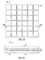
- FIG. 1Ais an illustration of a top view of an array of OLED structures, in accordance with the teachings of this invention.
- FIG. 1Bis a side view of the array of FIG. 1A taken through line 1 B— 1 B;
- FIG. 2is a block diagram of an OLED pixel word array structure, each word being composed of 16 pixels;
- FIG. 3is a block diagram of an embodiment of an OLED pixel word circuit
- FIG. 4is schematic of logic circuitry in a word select circuit, in accordance with these teachings.
- FIG. 5is a simplified schematic of an embodiment of an OLED pixel circuit
- FIG. 6is a more detailed schematic of an OLED pixel circuit
- FIG. 7is a block diagram of display and control register clear connections for driving an OLED array.
- FIG. 8is a block diagram of an OLED pixel word structure showing a physical relationship of pixel circuits and a word select circuit to respective anodes of OLED pixels.
- the teachings in accordance with presently preferred embodiments of this inventionrelate to active matrix OLED displays. Such displays may be configured as micro-displays and incorporated into small, battery-powered devices such as electronic wristwatches. This particular field of use and application should not, however, be construed in any manner as a limitation upon the practice of the teachings of this invention.
- FIG. 1Ais an illustration of a top view of an array 100 of OLED structures, e.g., picture elements (pixels) or light emitting elements
- FIG. 1Bis a side view of array 100 taken through line 1 B— 1 B of FIG. 1 A.
- Each OLED structure of array 100is constructed to have a pixel circuit that includes an OLED and a static memory for storing data that represents an operational state of the OLED.
- Array 100may be generally considered to be a regular n ⁇ m array of pixels, where n may or may not be equal to m.
- Array 100includes a plurality of OLED structures, each of which has an anode electrode 105 .
- the anode electrodes 105are arranged in two dimensions, forming a planar display.
- the side view shown in FIG. 1Bdepicts the vertical structure of array 100 on, by example, a silicon chip 101 upon which anode electrodes 105 are patterned.
- Disposed below anode electrodes 105may be a light-blocking layer (not shown) to prevent OLED light or external light from reaching underlying circuitry.
- An organic layer 102 and a transparent cathode counter-electrode layer 103are disposed above anode electrodes 105 .
- an observermay view the OLED through its anode electrode 105 , but the preferred embodiment involves viewing the OLED through its cathode counter-electrode layer 103 . This is because the silicon substrate 101 is not transparent, but is opaque.
- a protective cover glass 104is attached to the silicon chip 101 over cathode electrode layer 103 to provide environmental protection for the OLED structure.
- a suitable getter for moisture absorptionmay also be positioned within a cover-glass-to-silicon seal, but outside the boundary of array 100 .
- data that defines a state of the pixelsmay be written to, and stored, in either a dynamic or static memory structure.
- the stored datamay also be read out from the memory structure, if it is so configured, for example, for purposes of electrical testing.
- a dynamic memory arraydata is stored on a capacitor and must be refreshed periodically, an operation that dissipates power.
- a static memorydata is stored in an electronic latch comprised of CMOS circuits, and virtually no power is dissipated to hold the data.
- the OLED display apparatusin accordance with the presently preferred embodiments of this invention uses static memory for low power dissipation.
- the organic materialis sandwiched between pixel electrodes of the underlying circuit and a counter-electrode.
- the pixel electrodeis typically the anode of the light emitting diode and the counter-electrode is typically the cathode.
- the displayis formed as a rectangular array of pixels that are turned ON or OFF as the displayed image requires. Each pixel has a pixel anode electrode and pixel circuits that control the electrical state of the anode relative to the counter-electrode.
- the pixel circuitsmay be constructed using thin-films formed on an insulating substrate, or they may be constructed using integrated circuit technology, preferably silicon-based.
- the pixel circuitcan be fabricated with (1) any suitable material, such as, for example, crystalline silicon, amorphous silicon, polysilicon, micro crystalline silicon, an organic semiconductor or a polymer semiconductor, and (2) disposed, for example, on a substrate of silicon, glass, plastic, ceramic, or sapphire (AL 2 O 3 ).
- the thin-film circuits on an insulating (dielectric) substratehave the advantages of lower cost and an ability to be fabricated into large displays.
- the use of crystalline silicon devicesis confined to small area arrays, but the circuits have higher performance and higher fabrication density than the thin-film circuits.
- the OLED circuitry in accordance with these teachingsis suitable for being implemented using a variety of fabrication techniques, but the crystalline silicon technology is the preferred embodiment. Since silicon substrates are opaque to visible light, light emission is preferably through the counter-electrode, which is preferably formed as a continuous sheet of transparent conductive material such as indium tin oxide, e.g., see counter-electrode layer 103 .
- arrayis used to refer to an array of pixels as well as to an array of anodes.
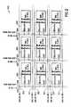
- FIG. 2is a block diagram of an OLED array 200 comprising a plurality of data storage devices or units, also referred to herein as word structures 205 .
- Each word structure 205is a static random access memory (SRAM) of, for example, 16 bits that correspond to sixteen pixels along a row of array 200 .
- SRAMstatic random access memory
- datais written into, and read out of, the array 16 bits at a time.
- each word structure 205The inputs to each word structure 205 are a column block select 204 , bit lines 203 , a word line read 202 and a word line write 201 .
- Datais written into word structure 205 from bit lines 203 when word line write 201 and column block select 204 lines are both activated, for example by switching them to a high state.
- Datais read from word structure 205 onto bit lines 203 when word line read 202 and column block select 204 are both activated. No operation is defined for the case where both word line read 202 and word line write 201 lines are active.
- each column block select 204relates to a column of array 200
- each word line write 201 and word line read 202relates to a row of array 200 .
- word line writes 201 and word line reads 202data can be written to, or read from, any of word structures 205 in array 200 .
- the total number of bit lines 203corresponds to the number of columns of pixels in array 200 . Since each word structure 205 represents 16 pixels, the number of column block selects 204 corresponds to the number of columns of pixels in array 200 divided by 16.
- Conventional SRAMstypically use complimentary bit lines, i.e., two lines per bit.
- the present inventionuses a single bit line per pixel column, thus reducing power dissipation as compared to the conventional design.
- a set of bit lines 203 representing data bits 1 - 16is configured as 16 single lines.
- reading data from the memory cells of a displayis less efficient than reading from a system memory external to the display because reading from the display typically has higher power dissipation and lower speed.
- reading data from the memory cells of the displayis useful when electrically testing the display. Nonetheless, an emphasis is placed on writing to the display rather than reading from the display. Accordingly, conventional SRAM design techniques such as pulsed word line addressing, bit line equalization and bit line sense circuitry are not required.
- FIG. 3is a block diagram of an OLED pixel word structure 205 .
- Word structure 205includes a word select circuit 300 and sixteen pixel circuits 400 .
- the inputs to word select circuit 300are column block select 204 , word line read 202 and word line write 201 .
- the outputs of word select circuit 300are word read 404 and word write 405 .
- the inputs to pixel circuit 400are a single bit line 203 , word read 404 and word write 405 .
- Word read 404 and word write 405are the local word-selected extensions of word line read 202 and word line write 201 , respectively.
- Word select circuit 300is shown to the left of pixel circuits 400 by way of example.
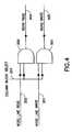
- FIG. 4shows the circuit details of some of the logic in word select circuit 300 .
- Word select circuit 300includes two AND gates 500 and 501 .
- AND gate 500The inputs to AND gate 500 are column block select 204 and word line read 202 .
- Word read 404is the output of AND gate 500 .
- word read 404goes high, i.e., active.
- the inputs to AND gate 501are column block select 204 and word line write 201 .
- Word write 405is the output of AND gate 501 .
- word write 405goes high, i.e., active.
- FIG. 5is a simplified schematic of the major functional elements of pixel circuit 400 in array 200 .
- Pixel circuit 400includes an SRAM cell 10 , a current source 20 connected to a voltage power supply V 1 , three switches 30 , 40 and 50 , a grounded gate p-type metal oxide semiconductor (PMOS) transistor 60 with its n-well connected to its source 64 , i.e., a floating well, and an OLED 70 connected to a power supply voltage V 2 .
- V 1is a positive voltage
- V 2is a negative voltage.
- the inputs to SRAM cell 10are a single bit line 203 , word read 404 , and word write 405 .
- bit line 203is a single bit line for inputting a signal that represents data to, and outputting a signal that represents the data from, SRAM cell 10 .
- Word write 405enables writing of data into SRAM cell 10 and word read 404 enables reading of data from SRAM cell 10 .
- the outputs of SRAM cell 10are bit line 203 , and a control line 8 .
- bit line 203is both an input and an output of SRAM cell 10 .
- Control line 8is for controlling switch 40 . With high states on both bit line 203 and word write 405 , a high state is written into SRAM cell 10 . When SRAM cell 10 stores a high state, control line 8 closes switch 40 . When SRAM cell 10 stores a low state, control line 8 opens switch 40 .
- V 1provides power for current source 20 .
- Current source 20produces an output current corresponding to a predetermined maximum brightness level of OLED 70 .
- a duty factor NOT 6is a pulse width modulated signal that is provided as an input common to all pixels in array 200 .
- a low state on duty factor NOT 6closes switch 30 .
- a high state on the duty factor NOT 6opens switch 30 .
- the duty factor NOT 6controls the average current through OLED 70 to set its luminance to a level of less than the maximum brightness.
- a reverse bias 7is a signal that is provided as an input common to all pixels in array 200 .
- a high state on reverse bias 7closes switch 50 .
- a low state on reverse bias 7opens switch 50 .
- PMOS transistor 60When switches 30 and 40 are closed and switch 50 is open, current flows from current source 20 , through switches 30 and 40 , and into source 64 of PMOS transistor 60 .
- PMOS transistor 60operates as a cascode stage to provide a greater voltage compliance range for current source 20 , as is known in the art.
- Current out the drain 62 of PMOS transistor 60flows into OLED 70 turning OLED 70 ON.
- Voltage compliance rangeis the range of output voltages over which the output current is essentially constant.
- a cascode stageis a common gate amplifier stage that improves the voltage compliance range by providing voltage gain.
- PMOS transistor 60When current is flowing through PMOS transistor 60 , it has a relatively low voltage, e.g., approximately 10 millivolts, across its drain 62 and source 64 . With current flowing, the voltage on drain 62 can be several volts above or below ground while the voltage on source 64 is at a minimum of one threshold voltage above ground and always higher than the voltage on its drain 62 . A threshold voltage is the minimum source to gate voltage required to maintain the transistor in the normal conducting region of operation. When no current is flowing into source 64 of PMOS transistor 60 , the voltage on source 64 does not go below ground.
- a threshold voltageis the minimum source to gate voltage required to maintain the transistor in the normal conducting region of operation.
- chargecan be trapped in its organic layers. This increases the forward bias voltage of the OLED required for a given current to flow.
- the trapped chargecan be removed by reverse-biasing the OLED, either periodically or at irregular intervals.
- OLED 70is reverse-biased by opening switch 30 , thus interrupting flow of current from current source 20 , closing switch 50 and switching V 2 from a negative voltage to a positive voltage.
- Closing switch 50grounds the source 64 and n-well of PMOS transistor 60 .
- the drain 62 of PMOS transistor 60is a p-diffusion.
- V 2is switched to a positive voltage, current flows from V 2 , through OLED 70 PMOS transistor 60 and switch 50 .
- the anode 72 of OLED 70is held at one diode voltage drop above ground.
- the reverse-bias voltage across OLED 70is the positive voltage of V 2 minus one diode drop.
- Reverse biasing of an OLEDdoes not need to be performed at frequent intervals. Instead, it can be performed at irregular intervals or when a display is not being viewed.
- the OLEDmay be driven during the day in a normal forward bias manner, and at night, when the image on the display is OFF, the OLED voltage can be reverse-biased.
- the OLEDcan be reverse-biased during a pulse width modulation brightness control cycle when the OLED is turned OFF.
- FIG. 6shows details of the pixel circuit 400 of FIG. 5 .
- V 1is set to +3V and V 2 is set to ⁇ 5V.
- SRAM cell 10includes n-type metal oxide semiconductor (NMOS) transistors 11 and 15 , and inverters 12 , 13 and 14 .
- NMOSn-type metal oxide semiconductor
- a high state on word write input 405causes NMOS transistor 11 to couple the logic state on bit line 203 to the input of inverter 12 .
- inverter 12The output of inverter 12 is an inverse of its input.
- the output of inverter 12is connected to the input of inverter 13 , and the input of inverter 14 , and it also provides the signal for control line 8 .
- Inverter 13has its output connected to the input of inverter 12 .
- inverter 12receives its input either from bit line 203 by a turned ON NMOS transistor 11 , or from the output of inverter 13 .
- the current drive of NMOS transistor 11is determined, in part, by a ratio of its channel width to its channel length.
- the current drives of inverter 12 and NMOS transistor 11are relatively stronger, e.g., about 10 times stronger, than the drive of inverter 13 . Accordingly, the input from bit line 203 , by way of a turned ON NMOS transistor 11 to inverter 12 , determines the state of SRAM cell 10 .
- NMOS transistor 11initially sets the state of inverter 12 , and inverter 13 feeds back, i.e., provides a latch signal, into inverter 12 to hold the state after the data level from NMOS transistor 11 is removed.
- NMOS transistor 11 , and inverters 12 and 13comprise a data latch.
- a PMOS transistor 40 Aserves the role of switch 40 (FIG. 5 ).
- Control line 8from the output of inverter 12 , is connected to the gate of PMOS transistor 40 A.
- word read 404is set high to cause NMOS transistor 15 to couple the output of inverter 14 to bit line 3 .
- the polarity of data read out of SRAM cell 10is the same as that previously written into SRAM cell 10 .
- SRAM cell 10may be simplified by eliminating inverter 14 and connecting the output of inverter 12 directly to NMOS transistor 15 .
- the data read out of SRAM cell 10is an inverse of that which was previously written into SRAM cell 10 , but it can be re-inverted in a bit line read circuit (not shown).
- inverter 14is included because it isolates pixel circuit 400 from noise on bit line 203 and from capacitance loading by bit line 203 during the read operation.
- a PMOS transistor 20 Aserves as a current source 20 (FIG. 5 ).
- a VREF 21is connected to the gate of PMOS transistor 20 A, and also to a similarly situated PMOS transistor in all of the other pixel circuits of array 200 .
- the previously mentioned light-blocking layermay, for instance, be used to distribute the +3V power of V 1 .
- the light-blocking layera conducting layer, is distributed and connected throughout the array providing a low-resistance path for V 1 power distribution. In this manner, the light-blocking layer performs two functions, i.e., light-blocking and power distribution.
- PMOS transistor 20 Ais a field effect transistor (FET) with a channel width (W), a channel length (L) and a gate to source voltage (V gs ) that are optimized within area constraints ( ⁇ W ⁇ L) to minimize effects of threshold voltage (V T ) and channel width variations on the uniformity of current through OLED 70 of the pixels throughout the array.
- FETfield effect transistor
- the channel lengthis determined by the seperation of drain and source diffusions as formed by the gate conductor.
- the channel widthis the drain or source dimension along the gate conductor. In saturation
- the drain currentis proportional to
- V dsis the drain to source voltage.
- VREF 21 voltageis set relative to V 1 and is adjusted to obtain a desired measured maximum brightness of OLED 70 , thereby removing the effect of current source transistor parameters and OLED efficiency on the overall maximum brightness of the display.
- the channel lengthis 79.12 microns
- the channel widthis 2.64 microns
- the gate to source voltage of PMOS transistor 20 Ais nominally ⁇ 1.1 V.
- a threshold voltage of ⁇ 0.6VPMOS transistor 20 A remains in saturation, i.e., produces constant current, as long as its source to drain voltage is greater than 0.5V.
- the static source to gate voltage of PMOS transistor 20 Ais greater than its threshold voltage. In other words, only 0.5V of overhead voltage is required to drive OLED 70 .
- the designis very power efficient. With this implementation, the variation of current from PMOS transistor 20 A, in pixels across the display, is less than 1.05:1.
- a PMOS transistor 30 Aserves the role of switch 30 (FIG. 5 ), and an NMOS transistor 50 A serves the role of switch 50 (FIG. 5 ).
- This configuration of componentsallows the duty factor NOT 6 and reverse bias 7 as shown in FIG. 5 to be combined in a single reverse bias/duty factor NOT 9 signal.
- Reverse bias/duty factor NOT 9is an input common to all pixels in array 200 .
- reverse bias/duty factor NOT 9is duty factor modulated to turn PMOS transistor 30 A ON and OFF rapidly, to duty factor modulate the current in OLED 70 .
- This digital control of the brightness of OLED 70is more uniform than controlling it by means of an analog voltage.
- NMOS transistor 50 Ais turned ON by reverse bias/duty factor NOT 9 when PMOS transistor 30 A is turned OFF to help linearize the pulse width modulation by discharging parasitic capacitances of transistors 20 A, 30 A, 40 A, 50 A and 60 . If not discharged, the parasitic wiring, drain to substrate, source to substrate and FET interelectrode capacitances will allow current to continue to flow into the OLED for a short period while PMOS transistor 30 A is OFF. The parasitic capacitances would tend to keep the voltage of PMOS transistor 60 source 64 high, allowing PMOS transistor 60 to continue conducting until source 64 is discharged.
- CMOS circuitryis susceptible to damage if it is exposed to a voltage exceeding a its breakdown voltage, which is typically 3.6V. Also, the lifespan of the organic layers is significantly shortened when subjected to temperatures greater than 100 degrees centigrade. If an OLED is shorted between its anode and cathode, then an excessive current may flow through the shorted OLED's pixel circuit. Such a current may generate heat and damage an adjacent pixel, and it may also interfere with the voltages supplied to other pixels in the display.
- pixel circuit 400includes a protection circuit comprising PMOS transistors 81 , 82 and 83 , and a resistor 84 .
- PMOS transistors 81 , 82 and 83When the pixel is in the OFF state, the voltage drop across OLED 70 is reduced so the voltage at drain 62 of PMOS transistor 60 becomes more negative.
- Each of PMOS transistors 81 , 82 and 83drops approximately 1V, so that the voltage at source 64 of PMOS transistor 60 is limited to about 3 volts more negative than ground. That is, PMOS transistors 81 , 82 and 83 provide a negative ( ⁇ 3V) voltage clamp to assure that the gate to drain voltage of PMOS transistor 60 does not exceed its breakdown voltage rating of 3.6V.
- the protection circuiteffectively limits the current that can flow through the other components of pixel circuit 400 .
- the voltage at drain 62is about 1.75V above ground.
- PMOS transistors 81 , 82 and 83have no effect when OLED 70 is ON.
- resistor 84limits the current that can flow, and the power that can be dissipated.
- PMOS transistors 81 , 82 and 83still clamp the voltage at drain 62 of PMOS transistor 60 to approximately ⁇ 3 volts, and any excess voltage is dropped across resistor 84 .
- resistor 84is manufactured of undoped polysilicon having 40,000 ohms of resistance.
- PMOS transistors 81 , 82 and 83 , and resistor 84also allow testing of OLED 70 , and through similarly situated components in other pixel circuits, all of the OLED pixels in array 200 . This done by setting V 2 to a negative voltage, e.g., ⁇ 7V, with respect to ground, and either allowing V 1 to float or setting it to ground. With this arrangement, current path is created from ground through PMOS transistors 81 , 82 and 83 , resistor 84 , OLED 70 to V 2 . Each of PMOS transistors 81 , 82 and 83 drop about 0.7V. OLED 70 is forward biased, and if it is good, then it turns ON. This test is useful, for example, to spot defects after OLED deposition and sealing prior to further assembly of the display.
- powercan be saved by managing the manner in which images are written to a display.
- display power dissipationis proportional to the brightness of a pixel, and the number of pixels that are ON, therefore a strategy to reduce the brightness of a pixel and the number pixels that are ON would result in a saving of power.
- array 200is installed in a display for a wristwatch, then the number of pixels required to show the time as hands of a clock is between 1 and 2% of the total number of pixels.
- a typical screen for textmight turn ON 10 to 20% of the pixels. Images may require an illumination of 50% of the pixels.
- gray scale imagesare produced by spatial dithering as opposed to frame sequential operation to eliminate the power required to write rapidly to the display, as would be required for frame sequential operation.
- the number of ON pixelsis usually less than 50%, and therefore power can be saved by clearing the display in one operation before writing new data to the display and by only writing to word structures that have pixels turned ON.
- the full displaycan be cleared using bit line and word line driver circuits outside the array. If all word line writes 201 and column block selects 204 are brought high, with low data states on all bit lines 203 , then low level data is written into all SRAM cells 10 in array 200 turning OFF all the pixels in the display. In the example of a wristwatch, the control for this function is issued by the watch processor prior to updating the display. Then, data is written only to pixels that need to be ON in the new displayed screen.
- the brightness when showing timecan be reduced to a relatively low luminance level, e.g., about 30 candelas/meter squared.
- This luminance levelshould be sufficient for nighttime use and for low contrast applications at room ambient light levels. For showing text and images in room ambient conditions, 100 candelas/meter squared should be sufficient. Only use in bright sunlight conditions require luminance levels of 500 candelas/meter squared.
- the reverse bias/Duty factor NOT 9should be in a high state.
- the connection of V 2 to the displayshould be opened to eliminate any OFF state OLED current or currents due to OLED shorts. Accordingly, the current path between V 1 and V 2 is broken so that no current flows through pixel circuit 400 .
- the standby current draw of SRAM cell 10can be reduced if the voltage of V 1 is reduced, but not set so low that the display losses its data. Lowering the supply voltage reduces the leakage current through inverters 12 , 13 and 14 , and thus lowers standby power.
- the control for standbyis provided by the watch processor.
- control signals for duty factor NOT 6 , reverse bias 7 , standby and clearcan be written into an a SRAM word structure that forms a display control register, as described below, that is not part of array 200 , but external to it. In this manner, the display control signals are part of the display and not located elsewhere in the watch, thus reducing the number of dedicated signal lines to the display.
- control registerOne function of the control register is to “clear” the display, i.e., turn all pixels OFF in one operation. That is, to clear the displayed image without addressing all of the individual pixels of the display. This is done so that the processor need write only the pixels that will be ON in the new image, thus reducing power dissipation and burden on the processor compared to writing all pixels of the display.
- FIG. 7shows the functional blocks of the display involved in writing to and reading from array 200 and a display control register 705 , and the control flow for the clear operation.
- the processor(not shown) writes a word into display control register 705 including one bit that is dedicated to the clear function.
- a wordhas 16 bits.
- the processorsends addresses, a read/write signal, a chip select signal, and image data to the display.
- one column select line 204(FIG. 2) is activated by a column block decoder 701
- one word line read 202(FIG. 2) or one word line write 201 (FIG. 2) is activated by a word line decoder 702
- appropriate bit lines 203(FIG. 2) are selected by bit line read/write drivers 703 .
- display control register 705is addressed for writing by the column block decoder 701 and word line decoder 702 , and the data bit for clear is applied to the bit line read/write drivers 703 and stored in display control register 705 .
- a clear line output 704 of display control register 705is then activated, applying a clear signal to column block decoder 701 , word line decoder 702 and bit line read/write drivers 703 , which causes a “zero” to be written to all pixels of array 200 simultaneously, turning OFF all OLEDs.
- the displayis designed to be addressed by the memory expansion bus of a microprocessor which transmits image data to the display in the form of words, each comprising the data for several pixels at a time, for example, 16 pixels at a time. Data may also be read out of the SRAM storage of the display, for instance for testing purposes, also a word at a time.
- word select circuitsare embedded in the display, for example, one such circuit for every horizontal group of 16 pixels. This necessitates a periodic shifting of the connections between the pixel circuits and the actual pixels to maintain a uniform, or constant, pixel pitch.
- FIG. 8is a block diagram of an OLED pixel word structure 205 showing a physical relationship of pixel circuits 400 and a word select circuit 300 to respective anodes of OLED pixels.
- Word structure 205is comprised of 16 pixel circuits 400 and one word select circuit 300 disposed along a row of array 200 .
- 16 OLED anode electrodes 105overlay word structure 205 , each anode being connected by a conductive via 802 to a metal conductor 801 of a corresponding pixel circuit 400 .
- Via 802 and conductor 801are part of a conductive path from pixel circuit 400 to anode 105 , i.e. a connection from resistor 84 to OLED 70 in FIG. 6 .
- FIG. 8is a block diagram of an OLED pixel word structure 205 showing a physical relationship of pixel circuits 400 and a word select circuit 300 to respective anodes of OLED pixels.
- Word structure 205is comprised of 16 pixel circuits 400 and one word select
- anode electrodes 105 and pixel circuits 400are shown adjacent to each other for clarity, it will be clear that in practice they overlap each other, at least in part.
- the average row-wise dimension of pixel circuit 400 and the pitch of anode electrode 105are 34.3 microns, while the row-wise pitch of word select circuit 300 is 8 microns.
- the row-wise dimension of each pixel circuit 400is reduced by 0.5 microns, i.e., from 34.3 microns to 33.8 microns, as compared to the anode electrodes 105 .
- via 802should be centered on each anode electrode 105 , or at least be located at the same relative position on each anode electrode 105 .
- conductor 801 of each pixel circuit 400has a sufficient row-wise extent to accommodate the shifting position of via 802 . The result is that the pitch of the OLED anodes is uniform throughout the array even though the pitch of the pixel circuits, to which the OLED anodes are connected, is not uniform.
- CMOS circuitsare incorporated into each pixel of an active matrix OLED display.
- the circuitsexhibit low power dissipation for battery operation, incorporate a constant current source for uniformity of brightness and reduced dependence of brightness on the characteristics of the OLED, and permit the use of a lower voltage circuit technology than the voltage which the OLED requires for operation.
- Each pixelincorporates an SRAM memory cell to control the state, ON or OFF, of the pixel and so does not require periodic refreshing.
- the circuitalso has a provision for application of reverse voltage when required to minimize deterioration of the OLED over time, a provision for duty factor control of luminance, and a current limiting resistor to isolate the effect of shorted pixels.
- the displayis addressed by the memory expansion bus of a microprocessor in the form of words of several pixels length, and the display data may be read out in the same form. Circuits for decoding the word address are embedded in the array of pixels that comprise the display. Furthermore, a provision is made to clear the display image in one operation so that a new image may be displayed by addressing only the pixels that are turned ON.
Landscapes
- Engineering & Computer Science (AREA)
- Computer Hardware Design (AREA)
- Physics & Mathematics (AREA)
- General Physics & Mathematics (AREA)
- Theoretical Computer Science (AREA)
- Microelectronics & Electronic Packaging (AREA)
- Control Of Indicators Other Than Cathode Ray Tubes (AREA)
- Electroluminescent Light Sources (AREA)
- Control Of El Displays (AREA)
- Led Devices (AREA)
- Devices For Indicating Variable Information By Combining Individual Elements (AREA)
- Non-Volatile Memory (AREA)
- Solid State Image Pick-Up Elements (AREA)
Abstract
Description
Claims (20)
Priority Applications (1)
| Application Number | Priority Date | Filing Date | Title |
|---|---|---|---|
| US10/390,809US6777712B2 (en) | 2001-01-04 | 2003-03-18 | Low-power organic light emitting diode pixel circuit |
Applications Claiming Priority (2)
| Application Number | Priority Date | Filing Date | Title |
|---|---|---|---|
| US09/754,489US6580657B2 (en) | 2001-01-04 | 2001-01-04 | Low-power organic light emitting diode pixel circuit |
| US10/390,809US6777712B2 (en) | 2001-01-04 | 2003-03-18 | Low-power organic light emitting diode pixel circuit |
Related Parent Applications (1)
| Application Number | Title | Priority Date | Filing Date |
|---|---|---|---|
| US09/754,489DivisionUS6580657B2 (en) | 2001-01-04 | 2001-01-04 | Low-power organic light emitting diode pixel circuit |
Publications (2)
| Publication Number | Publication Date |
|---|---|
| US20030179626A1 US20030179626A1 (en) | 2003-09-25 |
| US6777712B2true US6777712B2 (en) | 2004-08-17 |
Family
ID=25035022
Family Applications (2)
| Application Number | Title | Priority Date | Filing Date |
|---|---|---|---|
| US09/754,489Expired - LifetimeUS6580657B2 (en) | 2001-01-04 | 2001-01-04 | Low-power organic light emitting diode pixel circuit |
| US10/390,809Expired - LifetimeUS6777712B2 (en) | 2001-01-04 | 2003-03-18 | Low-power organic light emitting diode pixel circuit |
Family Applications Before (1)
| Application Number | Title | Priority Date | Filing Date |
|---|---|---|---|
| US09/754,489Expired - LifetimeUS6580657B2 (en) | 2001-01-04 | 2001-01-04 | Low-power organic light emitting diode pixel circuit |
Country Status (12)
| Country | Link |
|---|---|
| US (2) | US6580657B2 (en) |
| EP (2) | EP1362339B1 (en) |
| JP (2) | JP4038125B2 (en) |
| KR (1) | KR100526268B1 (en) |
| CN (1) | CN100336092C (en) |
| AT (1) | ATE412959T1 (en) |
| AU (1) | AU2002222301A1 (en) |
| CA (1) | CA2432530C (en) |
| DE (1) | DE60136389D1 (en) |
| IL (1) | IL156524A0 (en) |
| TW (1) | TW516243B (en) |
| WO (1) | WO2002054373A2 (en) |
Cited By (94)
| Publication number | Priority date | Publication date | Assignee | Title |
|---|---|---|---|---|
| US20030214466A1 (en)* | 2002-05-17 | 2003-11-20 | Semiconductor Energy Laboratory Co., Ltd. | Display apparatus and driving method thereof |
| US20030234392A1 (en)* | 2002-06-25 | 2003-12-25 | Nein-Hui Kung | Active matrix organic light emitting diode display pixel structure |
| US20040041752A1 (en)* | 2002-05-17 | 2004-03-04 | Hajime Kimura | Display apparatus and driving method thereof |
| US20040189559A1 (en)* | 2003-03-31 | 2004-09-30 | An Shih | Method and system for testing driver circuits of amoled |
| US20070008253A1 (en)* | 2005-07-06 | 2007-01-11 | Arokia Nathan | Method and system for driving a pixel circuit in an active matrix display |
| US20070063933A1 (en)* | 2005-09-13 | 2007-03-22 | Chung Bo Y | Emission control line driver and organic light emitting display using the emission control line driver |
| US20070080908A1 (en)* | 2003-09-23 | 2007-04-12 | Arokia Nathan | Circuit and method for driving an array of light emitting pixels |
| US20070146250A1 (en)* | 2002-05-17 | 2007-06-28 | Semiconductor Energy Laboratory Co., Ltd. | Display device |
| US20070195020A1 (en)* | 2006-02-10 | 2007-08-23 | Ignis Innovation, Inc. | Method and System for Light Emitting Device Displays |
| US20080191976A1 (en)* | 2004-06-29 | 2008-08-14 | Arokia Nathan | Voltage-Programming Scheme for Current-Driven Arnoled Displays |
| US7532209B2 (en) | 2002-05-17 | 2009-05-12 | Semiconductor Energy Laboratory Co., Ltd. | Display apparatus and driving method thereof |
| US20100033469A1 (en)* | 2004-12-15 | 2010-02-11 | Ignis Innovation Inc. | Method and system for programming, calibrating and driving a light emitting device display |
| US7719498B2 (en)* | 2001-02-21 | 2010-05-18 | Semiconductor Energy Laboratory Co., Ltd. | Light emitting device and electronic appliance |
| US20110128262A1 (en)* | 2009-12-01 | 2011-06-02 | Ignis Innovation Inc. | High resolution pixel architecture |
| US8026876B2 (en) | 2006-08-15 | 2011-09-27 | Ignis Innovation Inc. | OLED luminance degradation compensation |
| US8576217B2 (en) | 2011-05-20 | 2013-11-05 | Ignis Innovation Inc. | System and methods for extraction of threshold and mobility parameters in AMOLED displays |
| US8599191B2 (en) | 2011-05-20 | 2013-12-03 | Ignis Innovation Inc. | System and methods for extraction of threshold and mobility parameters in AMOLED displays |
| US8659518B2 (en) | 2005-01-28 | 2014-02-25 | Ignis Innovation Inc. | Voltage programmed pixel circuit, display system and driving method thereof |
| US8664644B2 (en) | 2001-02-16 | 2014-03-04 | Ignis Innovation Inc. | Pixel driver circuit and pixel circuit having the pixel driver circuit |
| US8743096B2 (en) | 2006-04-19 | 2014-06-03 | Ignis Innovation, Inc. | Stable driving scheme for active matrix displays |
| US8803417B2 (en) | 2009-12-01 | 2014-08-12 | Ignis Innovation Inc. | High resolution pixel architecture |
| US8901579B2 (en) | 2011-08-03 | 2014-12-02 | Ignis Innovation Inc. | Organic light emitting diode and method of manufacturing |
| US8907991B2 (en) | 2010-12-02 | 2014-12-09 | Ignis Innovation Inc. | System and methods for thermal compensation in AMOLED displays |
| US8922544B2 (en) | 2012-05-23 | 2014-12-30 | Ignis Innovation Inc. | Display systems with compensation for line propagation delay |
| US8994617B2 (en) | 2010-03-17 | 2015-03-31 | Ignis Innovation Inc. | Lifetime uniformity parameter extraction methods |
| US9070775B2 (en) | 2011-08-03 | 2015-06-30 | Ignis Innovations Inc. | Thin film transistor |
| US9093028B2 (en) | 2009-12-06 | 2015-07-28 | Ignis Innovation Inc. | System and methods for power conservation for AMOLED pixel drivers |
| US9111485B2 (en) | 2009-06-16 | 2015-08-18 | Ignis Innovation Inc. | Compensation technique for color shift in displays |
| US9134825B2 (en) | 2011-05-17 | 2015-09-15 | Ignis Innovation Inc. | Systems and methods for display systems with dynamic power control |
| US9153172B2 (en) | 2004-12-07 | 2015-10-06 | Ignis Innovation Inc. | Method and system for programming and driving active matrix light emitting device pixel having a controllable supply voltage |
| US9171504B2 (en) | 2013-01-14 | 2015-10-27 | Ignis Innovation Inc. | Driving scheme for emissive displays providing compensation for driving transistor variations |
| US9171500B2 (en) | 2011-05-20 | 2015-10-27 | Ignis Innovation Inc. | System and methods for extraction of parasitic parameters in AMOLED displays |
| US9190456B2 (en) | 2012-04-25 | 2015-11-17 | Ignis Innovation Inc. | High resolution display panel with emissive organic layers emitting light of different colors |
| US9275579B2 (en) | 2004-12-15 | 2016-03-01 | Ignis Innovation Inc. | System and methods for extraction of threshold and mobility parameters in AMOLED displays |
| US9280933B2 (en) | 2004-12-15 | 2016-03-08 | Ignis Innovation Inc. | System and methods for extraction of threshold and mobility parameters in AMOLED displays |
| US9305488B2 (en) | 2013-03-14 | 2016-04-05 | Ignis Innovation Inc. | Re-interpolation with edge detection for extracting an aging pattern for AMOLED displays |
| US9311859B2 (en) | 2009-11-30 | 2016-04-12 | Ignis Innovation Inc. | Resetting cycle for aging compensation in AMOLED displays |
| US9324268B2 (en) | 2013-03-15 | 2016-04-26 | Ignis Innovation Inc. | Amoled displays with multiple readout circuits |
| US9336717B2 (en) | 2012-12-11 | 2016-05-10 | Ignis Innovation Inc. | Pixel circuits for AMOLED displays |
| US9343006B2 (en) | 2012-02-03 | 2016-05-17 | Ignis Innovation Inc. | Driving system for active-matrix displays |
| US9378808B2 (en)* | 2014-10-17 | 2016-06-28 | M31 Technology Corporation | Pulse width modulation device |
| US9384698B2 (en) | 2009-11-30 | 2016-07-05 | Ignis Innovation Inc. | System and methods for aging compensation in AMOLED displays |
| US9385169B2 (en) | 2011-11-29 | 2016-07-05 | Ignis Innovation Inc. | Multi-functional active matrix organic light-emitting diode display |
| US9430958B2 (en) | 2010-02-04 | 2016-08-30 | Ignis Innovation Inc. | System and methods for extracting correlation curves for an organic light emitting device |
| US9437137B2 (en) | 2013-08-12 | 2016-09-06 | Ignis Innovation Inc. | Compensation accuracy |
| US9466240B2 (en) | 2011-05-26 | 2016-10-11 | Ignis Innovation Inc. | Adaptive feedback system for compensating for aging pixel areas with enhanced estimation speed |
| US9502653B2 (en) | 2013-12-25 | 2016-11-22 | Ignis Innovation Inc. | Electrode contacts |
| US9530349B2 (en) | 2011-05-20 | 2016-12-27 | Ignis Innovations Inc. | Charged-based compensation and parameter extraction in AMOLED displays |
| US9606607B2 (en) | 2011-05-17 | 2017-03-28 | Ignis Innovation Inc. | Systems and methods for display systems with dynamic power control |
| US9741282B2 (en) | 2013-12-06 | 2017-08-22 | Ignis Innovation Inc. | OLED display system and method |
| US9747834B2 (en) | 2012-05-11 | 2017-08-29 | Ignis Innovation Inc. | Pixel circuits including feedback capacitors and reset capacitors, and display systems therefore |
| US9761170B2 (en) | 2013-12-06 | 2017-09-12 | Ignis Innovation Inc. | Correction for localized phenomena in an image array |
| US9773439B2 (en) | 2011-05-27 | 2017-09-26 | Ignis Innovation Inc. | Systems and methods for aging compensation in AMOLED displays |
| US9786209B2 (en) | 2009-11-30 | 2017-10-10 | Ignis Innovation Inc. | System and methods for aging compensation in AMOLED displays |
| US9786223B2 (en) | 2012-12-11 | 2017-10-10 | Ignis Innovation Inc. | Pixel circuits for AMOLED displays |
| US9799246B2 (en) | 2011-05-20 | 2017-10-24 | Ignis Innovation Inc. | System and methods for extraction of threshold and mobility parameters in AMOLED displays |
| US9818376B2 (en) | 2009-11-12 | 2017-11-14 | Ignis Innovation Inc. | Stable fast programming scheme for displays |
| US9830857B2 (en) | 2013-01-14 | 2017-11-28 | Ignis Innovation Inc. | Cleaning common unwanted signals from pixel measurements in emissive displays |
| US9842889B2 (en) | 2014-11-28 | 2017-12-12 | Ignis Innovation Inc. | High pixel density array architecture |
| US9881532B2 (en) | 2010-02-04 | 2018-01-30 | Ignis Innovation Inc. | System and method for extracting correlation curves for an organic light emitting device |
| US9934725B2 (en) | 2013-03-08 | 2018-04-03 | Ignis Innovation Inc. | Pixel circuits for AMOLED displays |
| US9947293B2 (en) | 2015-05-27 | 2018-04-17 | Ignis Innovation Inc. | Systems and methods of reduced memory bandwidth compensation |
| US9952698B2 (en) | 2013-03-15 | 2018-04-24 | Ignis Innovation Inc. | Dynamic adjustment of touch resolutions on an AMOLED display |
| US10012678B2 (en) | 2004-12-15 | 2018-07-03 | Ignis Innovation Inc. | Method and system for programming, calibrating and/or compensating, and driving an LED display |
| US10013907B2 (en) | 2004-12-15 | 2018-07-03 | Ignis Innovation Inc. | Method and system for programming, calibrating and/or compensating, and driving an LED display |
| US10019941B2 (en) | 2005-09-13 | 2018-07-10 | Ignis Innovation Inc. | Compensation technique for luminance degradation in electro-luminance devices |
| US10074304B2 (en) | 2015-08-07 | 2018-09-11 | Ignis Innovation Inc. | Systems and methods of pixel calibration based on improved reference values |
| US10078984B2 (en) | 2005-02-10 | 2018-09-18 | Ignis Innovation Inc. | Driving circuit for current programmed organic light-emitting diode displays |
| US10089924B2 (en) | 2011-11-29 | 2018-10-02 | Ignis Innovation Inc. | Structural and low-frequency non-uniformity compensation |
| US10089921B2 (en) | 2010-02-04 | 2018-10-02 | Ignis Innovation Inc. | System and methods for extracting correlation curves for an organic light emitting device |
| US10163996B2 (en) | 2003-02-24 | 2018-12-25 | Ignis Innovation Inc. | Pixel having an organic light emitting diode and method of fabricating the pixel |
| US10163401B2 (en) | 2010-02-04 | 2018-12-25 | Ignis Innovation Inc. | System and methods for extracting correlation curves for an organic light emitting device |
| US10176736B2 (en) | 2010-02-04 | 2019-01-08 | Ignis Innovation Inc. | System and methods for extracting correlation curves for an organic light emitting device |
| US10176752B2 (en) | 2014-03-24 | 2019-01-08 | Ignis Innovation Inc. | Integrated gate driver |
| US10181282B2 (en) | 2015-01-23 | 2019-01-15 | Ignis Innovation Inc. | Compensation for color variations in emissive devices |
| US10192479B2 (en) | 2014-04-08 | 2019-01-29 | Ignis Innovation Inc. | Display system using system level resources to calculate compensation parameters for a display module in a portable device |
| US10204540B2 (en) | 2015-10-26 | 2019-02-12 | Ignis Innovation Inc. | High density pixel pattern |
| US10235933B2 (en) | 2005-04-12 | 2019-03-19 | Ignis Innovation Inc. | System and method for compensation of non-uniformities in light emitting device displays |
| US10311780B2 (en) | 2015-05-04 | 2019-06-04 | Ignis Innovation Inc. | Systems and methods of optical feedback |
| US10319307B2 (en) | 2009-06-16 | 2019-06-11 | Ignis Innovation Inc. | Display system with compensation techniques and/or shared level resources |
| US10373554B2 (en) | 2015-07-24 | 2019-08-06 | Ignis Innovation Inc. | Pixels and reference circuits and timing techniques |
| US10388221B2 (en) | 2005-06-08 | 2019-08-20 | Ignis Innovation Inc. | Method and system for driving a light emitting device display |
| US10410579B2 (en) | 2015-07-24 | 2019-09-10 | Ignis Innovation Inc. | Systems and methods of hybrid calibration of bias current |
| US10423254B2 (en) | 2015-05-29 | 2019-09-24 | Semiconductor Energy Laboratory Co., Ltd. | Semiconductor device and display device having semiconductor device |
| US10573231B2 (en) | 2010-02-04 | 2020-02-25 | Ignis Innovation Inc. | System and methods for extracting correlation curves for an organic light emitting device |
| US10586491B2 (en) | 2016-12-06 | 2020-03-10 | Ignis Innovation Inc. | Pixel circuits for mitigation of hysteresis |
| US10657895B2 (en) | 2015-07-24 | 2020-05-19 | Ignis Innovation Inc. | Pixels and reference circuits and timing techniques |
| US10714018B2 (en) | 2017-05-17 | 2020-07-14 | Ignis Innovation Inc. | System and method for loading image correction data for displays |
| US10867536B2 (en) | 2013-04-22 | 2020-12-15 | Ignis Innovation Inc. | Inspection system for OLED display panels |
| US10971078B2 (en) | 2018-02-12 | 2021-04-06 | Ignis Innovation Inc. | Pixel measurement through data line |
| US10996258B2 (en) | 2009-11-30 | 2021-05-04 | Ignis Innovation Inc. | Defect detection and correction of pixel circuits for AMOLED displays |
| US10997901B2 (en) | 2014-02-28 | 2021-05-04 | Ignis Innovation Inc. | Display system |
| US11025899B2 (en) | 2017-08-11 | 2021-06-01 | Ignis Innovation Inc. | Optical correction systems and methods for correcting non-uniformity of emissive display devices |
| US11715741B2 (en) | 2009-07-18 | 2023-08-01 | Semiconductor Energy Laboratory Co., Ltd. | Semiconductor device and method for manufacturing semiconductor device |
Families Citing this family (91)
| Publication number | Priority date | Publication date | Assignee | Title |
|---|---|---|---|---|
| JP3757797B2 (en)* | 2001-01-09 | 2006-03-22 | 株式会社日立製作所 | Organic LED display and driving method thereof |
| US6734636B2 (en)* | 2001-06-22 | 2004-05-11 | International Business Machines Corporation | OLED current drive pixel circuit |
| JP4873677B2 (en)* | 2001-09-06 | 2012-02-08 | 東北パイオニア株式会社 | Driving device for light emitting display panel |
| TW563088B (en)* | 2001-09-17 | 2003-11-21 | Semiconductor Energy Lab | Light emitting device, method of driving a light emitting device, and electronic equipment |
| JP3810725B2 (en) | 2001-09-21 | 2006-08-16 | 株式会社半導体エネルギー研究所 | LIGHT EMITTING DEVICE AND ELECTRONIC DEVICE |
| TW518543B (en)* | 2001-11-14 | 2003-01-21 | Ind Tech Res Inst | Integrated current driving framework of active matrix OLED |
| US7167169B2 (en)* | 2001-11-20 | 2007-01-23 | Toppoly Optoelectronics Corporation | Active matrix oled voltage drive pixel circuit |
| GB0205859D0 (en)* | 2002-03-13 | 2002-04-24 | Koninkl Philips Electronics Nv | Electroluminescent display device |
| US6914387B2 (en)* | 2002-05-08 | 2005-07-05 | Sumitomo Electric Industries, Ltd. | Driving circuit for a light emitting element |
| JP2004157467A (en)* | 2002-11-08 | 2004-06-03 | Tohoku Pioneer Corp | Driving method and driving-gear of active type light emitting display panel |
| EP1563478A2 (en)* | 2002-11-15 | 2005-08-17 | Koninklijke Philips Electronics N.V. | Display device, electric device comprising such a display device and method for driving a display device |
| EP1570458B1 (en)* | 2002-12-04 | 2012-01-11 | Koninklijke Philips Electronics N.V. | An organic led display device and a method for driving such a device |
| CN1310204C (en)* | 2003-01-09 | 2007-04-11 | 友达光电股份有限公司 | organic light emitting display |
| TW572302U (en)* | 2003-04-08 | 2004-01-11 | Richtek Technology Corp | Energy-saving type auto-contrast compensation device of OLED |
| JP4425574B2 (en)* | 2003-05-16 | 2010-03-03 | 株式会社半導体エネルギー研究所 | Element substrate and light emitting device |
| JP4599819B2 (en)* | 2003-09-16 | 2010-12-15 | ソニー株式会社 | Display device, light receiving device, communication method, program, and communication system |
| WO2005029456A1 (en)* | 2003-09-23 | 2005-03-31 | Ignis Innovation Inc. | Circuit and method for driving an array of light emitting pixels |
| US7221332B2 (en)* | 2003-12-19 | 2007-05-22 | Eastman Kodak Company | 3D stereo OLED display |
| US7859494B2 (en)* | 2004-01-02 | 2010-12-28 | Samsung Electronics Co., Ltd. | Display device and driving method thereof |
| GB0405807D0 (en) | 2004-03-16 | 2004-04-21 | Koninkl Philips Electronics Nv | Active matrix display devices |
| TWI324332B (en)* | 2004-03-30 | 2010-05-01 | Au Optronics Corp | Display array and display panel |
| JP2005308857A (en)* | 2004-04-19 | 2005-11-04 | Sony Corp | Active matrix type display apparatus and driving method for the same |
| KR101142994B1 (en) | 2004-05-20 | 2012-05-08 | 삼성전자주식회사 | Display device and driving method thereof |
| US20050258867A1 (en)* | 2004-05-21 | 2005-11-24 | Seiko Epson Corporation | Electronic circuit, electro-optical device, electronic device and electronic apparatus |
| US20060001614A1 (en)* | 2004-07-02 | 2006-01-05 | Wei-Chieh Hsueh | Apparatus for refreshing voltage data in display pixel circuit and organic light emitting diode display using the same |
| US7136303B2 (en)* | 2004-08-31 | 2006-11-14 | Broadcom Corporation | System and method using a one-time programmable memory cell |
| US7139189B2 (en)* | 2004-09-24 | 2006-11-21 | Intel Corporation | State-retentive mixed register file array |
| US8362525B2 (en)* | 2005-01-14 | 2013-01-29 | Nantero Inc. | Field effect device having a channel of nanofabric and methods of making same |
| WO2007063814A1 (en)* | 2005-12-02 | 2007-06-07 | Semiconductor Energy Laboratory Co., Ltd. | Semiconductor device, display device, and electronic device |
| US7545348B2 (en) | 2006-01-04 | 2009-06-09 | Tpo Displays Corp. | Pixel unit and display and electronic device utilizing the same |
| US9269322B2 (en) | 2006-01-09 | 2016-02-23 | Ignis Innovation Inc. | Method and system for driving an active matrix display circuit |
| US9489891B2 (en) | 2006-01-09 | 2016-11-08 | Ignis Innovation Inc. | Method and system for driving an active matrix display circuit |
| WO2007079572A1 (en) | 2006-01-09 | 2007-07-19 | Ignis Innovation Inc. | Method and system for driving an active matrix display circuit |
| US7471588B2 (en)* | 2006-05-05 | 2008-12-30 | Altera Corporation | Dual port random-access-memory circuitry |
| US7583244B2 (en)* | 2006-05-11 | 2009-09-01 | Ansaldo Sts Usa, Inc. | Signal apparatus, light emitting diode (LED) drive circuit, LED display circuit, and display system including the same |
| TW200816870A (en)* | 2006-09-21 | 2008-04-01 | Beyond Innovation Tech Co Ltd | Circuit and method for driving light source |
| TWI326066B (en)* | 2006-09-22 | 2010-06-11 | Au Optronics Corp | Organic light emitting diode display and related pixel circuit |
| US7440312B2 (en)* | 2006-10-02 | 2008-10-21 | Analog Devices, Inc. | Memory write timing system |
| JP2008180802A (en)* | 2007-01-23 | 2008-08-07 | Eastman Kodak Co | Active matrix display device |
| JP5242076B2 (en)* | 2007-04-13 | 2013-07-24 | グローバル・オーエルイーディー・テクノロジー・リミテッド・ライアビリティ・カンパニー | Active matrix display device |
| JP5270120B2 (en)* | 2007-07-25 | 2013-08-21 | グローバル・オーエルイーディー・テクノロジー・リミテッド・ライアビリティ・カンパニー | Dual display device |
| KR100904737B1 (en)* | 2007-12-20 | 2009-06-26 | 주식회사 하이닉스반도체 | Semiconductor memory device having threshold voltage switching device and information storage method |
| EP2277163B1 (en) | 2008-04-18 | 2018-11-21 | Ignis Innovation Inc. | System and driving method for light emitting device display |
| CN101261810B (en)* | 2008-04-21 | 2010-04-14 | 上海大学 | A pixel driving circuit in a silicon-based organic light-emitting display device |
| CA2637343A1 (en) | 2008-07-29 | 2010-01-29 | Ignis Innovation Inc. | Improving the display source driver |
| JPWO2010024053A1 (en)* | 2008-08-26 | 2012-01-26 | シャープ株式会社 | Image display device |
| JP4693009B2 (en) | 2008-10-07 | 2011-06-01 | 奇美電子股▲ふん▼有限公司 | Active matrix display device and portable device including the same |
| US9370075B2 (en) | 2008-12-09 | 2016-06-14 | Ignis Innovation Inc. | System and method for fast compensation programming of pixels in a display |
| SI22945A (en)* | 2008-12-16 | 2010-06-30 | IDS@d@o@o | Procedure for battery based and passive power supply of rfid labels and switching circuit for performing this procedure |
| US8125472B2 (en)* | 2009-06-09 | 2012-02-28 | Global Oled Technology Llc | Display device with parallel data distribution |
| US9058786B2 (en)* | 2009-10-14 | 2015-06-16 | Innolux Corporation | Active matrix type liquid crystal display device and related driving methods |
| DE102010019667B4 (en)* | 2010-04-28 | 2014-02-20 | Fraunhofer-Gesellschaft zur Förderung der angewandten Forschung e.V. | Circuit arrangement for arranged in a two-dimensional matrix organic light-emitting diodes |
| JP5268117B2 (en) | 2010-10-25 | 2013-08-21 | 群創光電股▲ふん▼有限公司 | Display device and electronic apparatus including the same |
| US9351368B2 (en) | 2013-03-08 | 2016-05-24 | Ignis Innovation Inc. | Pixel circuits for AMOLED displays |
| US9886899B2 (en) | 2011-05-17 | 2018-02-06 | Ignis Innovation Inc. | Pixel Circuits for AMOLED displays |
| US20140368491A1 (en) | 2013-03-08 | 2014-12-18 | Ignis Innovation Inc. | Pixel circuits for amoled displays |
| US9881587B2 (en) | 2011-05-28 | 2018-01-30 | Ignis Innovation Inc. | Systems and methods for operating pixels in a display to mitigate image flicker |
| EP2542025B1 (en)* | 2011-06-28 | 2018-09-26 | Rohm Co., Ltd. | A power supply system for a display panel |
| JP5733077B2 (en)* | 2011-07-26 | 2015-06-10 | セイコーエプソン株式会社 | ELECTRO-OPTICAL DEVICE, ELECTRO-OPTICAL DEVICE POWER SUPPLY METHOD, AND ELECTRONIC DEVICE |
| JP2012118552A (en)* | 2012-01-16 | 2012-06-21 | Global Oled Technology Llc | Dual display device |
| CA2894717A1 (en) | 2015-06-19 | 2016-12-19 | Ignis Innovation Inc. | Optoelectronic device characterization in array with shared sense line |
| US9230473B2 (en)* | 2013-06-24 | 2016-01-05 | Microsoft Technology Licensing, Llc | Dual duty cycle OLED to enable dynamic control for reduced motion blur control with constant brightness in augmented reality experiences |
| US20150213752A1 (en)* | 2014-01-28 | 2015-07-30 | Nvidia Corporation | Adjustable screen display size for an electronic device |
| CA2873476A1 (en) | 2014-12-08 | 2016-06-08 | Ignis Innovation Inc. | Smart-pixel display architecture |
| CA2886862A1 (en) | 2015-04-01 | 2016-10-01 | Ignis Innovation Inc. | Adjusting display brightness for avoiding overheating and/or accelerated aging |
| CA2908285A1 (en) | 2015-10-14 | 2017-04-14 | Ignis Innovation Inc. | Driver with multiple color pixel structure |
| US11600234B2 (en) | 2015-10-15 | 2023-03-07 | Ordos Yuansheng Optoelectronics Co., Ltd. | Display substrate and driving method thereof |
| CN105185816A (en) | 2015-10-15 | 2015-12-23 | 京东方科技集团股份有限公司 | Array substrate, manufacturing method, and display device |
| CN106448564B (en) | 2016-12-20 | 2019-06-25 | 京东方科技集团股份有限公司 | A kind of OLED pixel circuit and its driving method, display device |
| US10276105B2 (en)* | 2017-06-07 | 2019-04-30 | Qualcomm Incorporated | Reversible bias organic light-emitting diode (OLED) drive circuit without initialization voltage |
| WO2019217242A1 (en)* | 2018-05-08 | 2019-11-14 | Apple Inc. | Memory-in-pixel display |
| CN111402782B (en)* | 2018-12-14 | 2021-09-03 | 成都辰显光电有限公司 | Digital driving pixel circuit and method for digitally driving pixel |
| CN115735244A (en)* | 2019-08-23 | 2023-03-03 | 京东方科技集团股份有限公司 | Pixel circuit and driving method, display substrate and driving method, display device |
| US12266303B2 (en) | 2019-08-23 | 2025-04-01 | Boe Technology Group Co., Ltd. | Display device and manufacturing method thereof |
| US11569482B2 (en) | 2019-08-23 | 2023-01-31 | Beijing Boe Technology Development Co., Ltd. | Display panel and manufacturing method thereof, display device |
| US11930664B2 (en) | 2019-08-23 | 2024-03-12 | Boe Technology Group Co., Ltd. | Display device with transistors oriented in directions intersecting direction of driving transistor and manufacturing method thereof |
| CN114864647B (en) | 2019-08-23 | 2025-03-28 | 京东方科技集团股份有限公司 | Display device and method for manufacturing the same |
| CN112703605B (en) | 2019-08-23 | 2025-01-10 | 京东方科技集团股份有限公司 | Display device, manufacturing method thereof, and drive substrate |
| US12120914B2 (en) | 2019-08-23 | 2024-10-15 | Boe Technology Group Co., Ltd. | Display device and manufacturing method thereof |
| CN112771674B (en) | 2019-08-27 | 2022-02-22 | 京东方科技集团股份有限公司 | Electronic device substrate, manufacturing method thereof and electronic device |
| CN110634443B (en)* | 2019-09-24 | 2021-01-26 | 京东方科技集团股份有限公司 | Light emitting element protection circuit and method for driving light emitting element protection circuit |
| KR102137639B1 (en)* | 2020-01-23 | 2020-07-27 | 주식회사 사피엔반도체 | Minimulized pixel circuit |
| US12236863B2 (en)* | 2020-01-28 | 2025-02-25 | OLEDWorks LLC | OLED display with protection circuit |
| FR3112243A1 (en)* | 2020-07-02 | 2022-01-07 | Microoled | THIN-LAYER MATRIX OPTOELECTRONIC DEVICE |
| CN113963667B (en) | 2020-07-21 | 2023-04-18 | 京东方科技集团股份有限公司 | Display device and driving method thereof |
| US20220165208A1 (en)* | 2020-11-25 | 2022-05-26 | Jasper Display Corp. | Hybrid pixel backplane and driving method |
| CN115298730A (en)* | 2021-02-23 | 2022-11-04 | 京东方科技集团股份有限公司 | Display panel and display device |
| CN114863879B (en)* | 2022-05-23 | 2023-05-02 | 惠科股份有限公司 | Organic light emitting diode control circuit and display panel |
| CN114974120B (en)* | 2022-07-13 | 2022-12-06 | 北京京东方技术开发有限公司 | Semiconductor substrate, driving method thereof, and semiconductor display device |
| WO2024016350A1 (en) | 2022-07-22 | 2024-01-25 | 京东方科技集团股份有限公司 | Pixel driving circuit and driving method therefor, and display panel and display apparatus |
| KR20240151321A (en) | 2023-04-10 | 2024-10-18 | 삼성디스플레이 주식회사 | Pixel and display device including the same |
Citations (18)
| Publication number | Priority date | Publication date | Assignee | Title |
|---|---|---|---|---|
| US4996523A (en)* | 1988-10-20 | 1991-02-26 | Eastman Kodak Company | Electroluminescent storage display with improved intensity driver circuits |
| US5353251A (en) | 1992-09-21 | 1994-10-04 | Sharp Kabushiki Kaisha | Memory cell circuit with single bit line latch |
| US5471225A (en) | 1993-04-28 | 1995-11-28 | Dell Usa, L.P. | Liquid crystal display with integrated frame buffer |
| US5682174A (en) | 1995-02-16 | 1997-10-28 | Texas Instruments Incorporated | Memory cell array for digital spatial light modulator |
| US5689471A (en) | 1995-01-24 | 1997-11-18 | Cypress Semiconductor Corp. | Dummy cell for providing a reference voltage in a memory array |
| US5712652A (en) | 1995-02-16 | 1998-01-27 | Kabushiki Kaisha Toshiba | Liquid crystal display device |
| US5903246A (en) | 1997-04-04 | 1999-05-11 | Sarnoff Corporation | Circuit and method for driving an organic light emitting diode (O-LED) display |
| WO1999038148A1 (en) | 1998-01-23 | 1999-07-29 | Fed Corporation | High resolution active matrix display system on a chip with high duty cycle for full brightness |
| WO1999042983A1 (en) | 1998-02-18 | 1999-08-26 | Cambridge Display Technology Ltd. | Electroluminescent devices |
| US5952789A (en) | 1997-04-14 | 1999-09-14 | Sarnoff Corporation | Active matrix organic light emitting diode (amoled) display pixel structure and data load/illuminate circuit therefor |
| US6023259A (en) | 1997-07-11 | 2000-02-08 | Fed Corporation | OLED active matrix using a single transistor current mode pixel design |
| EP1005013A1 (en) | 1998-11-25 | 2000-05-31 | Lucent Technologies Inc. | Display comprising organic smart pixels |
| US6229506B1 (en)* | 1997-04-23 | 2001-05-08 | Sarnoff Corporation | Active matrix light emitting diode pixel structure and concomitant method |
| US6339417B1 (en) | 1998-05-15 | 2002-01-15 | Inviso, Inc. | Display system having multiple memory elements per pixel |
| US6351078B1 (en)* | 2000-08-25 | 2002-02-26 | Industrial Technology Research Institute | Pixel structure of an organic light-emitting diode display device |
| US20020030064A1 (en) | 2000-03-17 | 2002-03-14 | Frank Lacout | Device and method for sampling and mixing products |
| US6459611B2 (en) | 1997-11-28 | 2002-10-01 | Stmicroelectronics S.R.L. | Low power SRAM memory cell having a single bit line |
| US6469405B1 (en)* | 1999-01-29 | 2002-10-22 | Seiko Instruments Inc. | Constant-current output driver with reduced over-shoot |
Family Cites Families (15)
| Publication number | Priority date | Publication date | Assignee | Title |
|---|---|---|---|---|
| US5198803A (en)* | 1990-06-06 | 1993-03-30 | Opto Tech Corporation | Large scale movie display system with multiple gray levels |
| US5151632A (en)* | 1991-03-22 | 1992-09-29 | General Motors Corporation | Flat panel emissive display with redundant circuit |
| JP3476241B2 (en)* | 1994-02-25 | 2003-12-10 | 株式会社半導体エネルギー研究所 | Display method of active matrix type display device |
| US5723950A (en)* | 1996-06-10 | 1998-03-03 | Motorola | Pre-charge driver for light emitting devices and method |
| JPH10161563A (en)* | 1996-11-29 | 1998-06-19 | Tdk Corp | Organic EL display |
| US6072517A (en)* | 1997-01-17 | 2000-06-06 | Xerox Corporation | Integrating xerographic light emitter array with grey scale |
| JP4251377B2 (en)* | 1997-04-23 | 2009-04-08 | 宇東科技股▲ふん▼有限公司 | Active matrix light emitting diode pixel structure and method |
| US6175345B1 (en)* | 1997-06-02 | 2001-01-16 | Canon Kabushiki Kaisha | Electroluminescence device, electroluminescence apparatus, and production methods thereof |
| JP3767877B2 (en)* | 1997-09-29 | 2006-04-19 | 三菱化学株式会社 | Active matrix light emitting diode pixel structure and method thereof |
| JP3252897B2 (en)* | 1998-03-31 | 2002-02-04 | 日本電気株式会社 | Element driving device and method, image display device |
| JP4092857B2 (en)* | 1999-06-17 | 2008-05-28 | ソニー株式会社 | Image display device |
| JP4627822B2 (en)* | 1999-06-23 | 2011-02-09 | 株式会社半導体エネルギー研究所 | Display device |
| TW482992B (en)* | 1999-09-24 | 2002-04-11 | Semiconductor Energy Lab | El display device and driving method thereof |
| TW484117B (en)* | 1999-11-08 | 2002-04-21 | Semiconductor Energy Lab | Electronic device |
| US20020030647A1 (en)* | 2000-06-06 | 2002-03-14 | Michael Hack | Uniform active matrix oled displays |
- 2001
- 2001-01-04USUS09/754,489patent/US6580657B2/ennot_activeExpired - Lifetime
- 2001-12-21WOPCT/GB2001/005736patent/WO2002054373A2/enactiveIP Right Grant
- 2001-12-21ILIL15652401Apatent/IL156524A0/enunknown
- 2001-12-21DEDE60136389Tpatent/DE60136389D1/ennot_activeExpired - Lifetime
- 2001-12-21CACA002432530Apatent/CA2432530C/ennot_activeExpired - Fee Related
- 2001-12-21CNCNB018217656Apatent/CN100336092C/ennot_activeExpired - Fee Related
- 2001-12-21JPJP2002555396Apatent/JP4038125B2/ennot_activeExpired - Fee Related
- 2001-12-21KRKR10-2003-7008902Apatent/KR100526268B1/ennot_activeExpired - Fee Related
- 2001-12-21EPEP01272506Apatent/EP1362339B1/ennot_activeExpired - Lifetime
- 2001-12-21AUAU2002222301Apatent/AU2002222301A1/ennot_activeAbandoned
- 2001-12-21ATAT01272506Tpatent/ATE412959T1/ennot_activeIP Right Cessation
- 2001-12-21EPEP06019722Apatent/EP1732058A3/ennot_activeWithdrawn
- 2001-12-28TWTW090132765Apatent/TW516243B/ennot_activeIP Right Cessation
- 2003
- 2003-03-18USUS10/390,809patent/US6777712B2/ennot_activeExpired - Lifetime
- 2007
- 2007-06-20JPJP2007162127Apatent/JP4276273B2/ennot_activeExpired - Fee Related
Patent Citations (18)
| Publication number | Priority date | Publication date | Assignee | Title |
|---|---|---|---|---|
| US4996523A (en)* | 1988-10-20 | 1991-02-26 | Eastman Kodak Company | Electroluminescent storage display with improved intensity driver circuits |
| US5353251A (en) | 1992-09-21 | 1994-10-04 | Sharp Kabushiki Kaisha | Memory cell circuit with single bit line latch |
| US5471225A (en) | 1993-04-28 | 1995-11-28 | Dell Usa, L.P. | Liquid crystal display with integrated frame buffer |
| US5689471A (en) | 1995-01-24 | 1997-11-18 | Cypress Semiconductor Corp. | Dummy cell for providing a reference voltage in a memory array |
| US5682174A (en) | 1995-02-16 | 1997-10-28 | Texas Instruments Incorporated | Memory cell array for digital spatial light modulator |
| US5712652A (en) | 1995-02-16 | 1998-01-27 | Kabushiki Kaisha Toshiba | Liquid crystal display device |
| US5903246A (en) | 1997-04-04 | 1999-05-11 | Sarnoff Corporation | Circuit and method for driving an organic light emitting diode (O-LED) display |
| US5952789A (en) | 1997-04-14 | 1999-09-14 | Sarnoff Corporation | Active matrix organic light emitting diode (amoled) display pixel structure and data load/illuminate circuit therefor |
| US6229506B1 (en)* | 1997-04-23 | 2001-05-08 | Sarnoff Corporation | Active matrix light emitting diode pixel structure and concomitant method |
| US6023259A (en) | 1997-07-11 | 2000-02-08 | Fed Corporation | OLED active matrix using a single transistor current mode pixel design |
| US6459611B2 (en) | 1997-11-28 | 2002-10-01 | Stmicroelectronics S.R.L. | Low power SRAM memory cell having a single bit line |
| WO1999038148A1 (en) | 1998-01-23 | 1999-07-29 | Fed Corporation | High resolution active matrix display system on a chip with high duty cycle for full brightness |
| WO1999042983A1 (en) | 1998-02-18 | 1999-08-26 | Cambridge Display Technology Ltd. | Electroluminescent devices |
| US6339417B1 (en) | 1998-05-15 | 2002-01-15 | Inviso, Inc. | Display system having multiple memory elements per pixel |
| EP1005013A1 (en) | 1998-11-25 | 2000-05-31 | Lucent Technologies Inc. | Display comprising organic smart pixels |
| US6469405B1 (en)* | 1999-01-29 | 2002-10-22 | Seiko Instruments Inc. | Constant-current output driver with reduced over-shoot |
| US20020030064A1 (en) | 2000-03-17 | 2002-03-14 | Frank Lacout | Device and method for sampling and mixing products |
| US6351078B1 (en)* | 2000-08-25 | 2002-02-26 | Industrial Technology Research Institute | Pixel structure of an organic light-emitting diode display device |
Non-Patent Citations (16)
Cited By (206)
| Publication number | Priority date | Publication date | Assignee | Title |
|---|---|---|---|---|
| US8890220B2 (en) | 2001-02-16 | 2014-11-18 | Ignis Innovation, Inc. | Pixel driver circuit and pixel circuit having control circuit coupled to supply voltage |
| US8664644B2 (en) | 2001-02-16 | 2014-03-04 | Ignis Innovation Inc. | Pixel driver circuit and pixel circuit having the pixel driver circuit |
| US7719498B2 (en)* | 2001-02-21 | 2010-05-18 | Semiconductor Energy Laboratory Co., Ltd. | Light emitting device and electronic appliance |
| US8780018B2 (en) | 2001-02-21 | 2014-07-15 | Semiconductor Energy Laboratory Co., Ltd. | Light emitting device and electronic appliance |
| US9040996B2 (en) | 2001-02-21 | 2015-05-26 | Semiconductor Energy Laboratory Co., Ltd. | Light emitting device and electronic appliance |
| US8120557B2 (en) | 2001-02-21 | 2012-02-21 | Semiconductor Energy Laboratory Co., Ltd. | Light emitting device and electronic appliance |
| US9431466B2 (en) | 2001-02-21 | 2016-08-30 | Semiconductor Energy Laboratory Co., Ltd. | Light emitting device and electronic appliance |
| US9886895B2 (en) | 2001-02-21 | 2018-02-06 | Semiconductor Energy Laboratory Co., Ltd. | Light emitting device and electronic appliance |
| US20100201721A1 (en)* | 2001-02-21 | 2010-08-12 | Semiconductor Energy Laboratory Co., Ltd. | Light Emitting Device and Electronic Appliance |
| US20070146250A1 (en)* | 2002-05-17 | 2007-06-28 | Semiconductor Energy Laboratory Co., Ltd. | Display device |
| US7474285B2 (en) | 2002-05-17 | 2009-01-06 | Semiconductor Energy Laboratory Co., Ltd. | Display apparatus and driving method thereof |
| US7511687B2 (en)* | 2002-05-17 | 2009-03-31 | Semiconductor Energy Laboratory Co., Ltd. | Display device, electronic apparatus and navigation system |
| US7532209B2 (en) | 2002-05-17 | 2009-05-12 | Semiconductor Energy Laboratory Co., Ltd. | Display apparatus and driving method thereof |
| US20040041752A1 (en)* | 2002-05-17 | 2004-03-04 | Hajime Kimura | Display apparatus and driving method thereof |
| US7852297B2 (en) | 2002-05-17 | 2010-12-14 | Semiconductor Energy Laboratory Co., Ltd. | Display device |
| US20030214466A1 (en)* | 2002-05-17 | 2003-11-20 | Semiconductor Energy Laboratory Co., Ltd. | Display apparatus and driving method thereof |
| US20030234392A1 (en)* | 2002-06-25 | 2003-12-25 | Nein-Hui Kung | Active matrix organic light emitting diode display pixel structure |
| US10163996B2 (en) | 2003-02-24 | 2018-12-25 | Ignis Innovation Inc. | Pixel having an organic light emitting diode and method of fabricating the pixel |
| US7116295B2 (en)* | 2003-03-31 | 2006-10-03 | Tpo Displays Corp. | Method and system for testing driver circuits of amoled |
| US20040189559A1 (en)* | 2003-03-31 | 2004-09-30 | An Shih | Method and system for testing driver circuits of amoled |
| US20070080908A1 (en)* | 2003-09-23 | 2007-04-12 | Arokia Nathan | Circuit and method for driving an array of light emitting pixels |
| US8941697B2 (en) | 2003-09-23 | 2015-01-27 | Ignis Innovation Inc. | Circuit and method for driving an array of light emitting pixels |
| US9472139B2 (en) | 2003-09-23 | 2016-10-18 | Ignis Innovation Inc. | Circuit and method for driving an array of light emitting pixels |
| US7978187B2 (en) | 2003-09-23 | 2011-07-12 | Ignis Innovation Inc. | Circuit and method for driving an array of light emitting pixels |
| US9852689B2 (en) | 2003-09-23 | 2017-12-26 | Ignis Innovation Inc. | Circuit and method for driving an array of light emitting pixels |
| US9472138B2 (en) | 2003-09-23 | 2016-10-18 | Ignis Innovation Inc. | Pixel driver circuit with load-balance in current mirror circuit |
| US10089929B2 (en) | 2003-09-23 | 2018-10-02 | Ignis Innovation Inc. | Pixel driver circuit with load-balance in current mirror circuit |
| US8553018B2 (en) | 2003-09-23 | 2013-10-08 | Ignis Innovation Inc. | Circuit and method for driving an array of light emitting pixels |
| US20080191976A1 (en)* | 2004-06-29 | 2008-08-14 | Arokia Nathan | Voltage-Programming Scheme for Current-Driven Arnoled Displays |
| USRE47257E1 (en) | 2004-06-29 | 2019-02-26 | Ignis Innovation Inc. | Voltage-programming scheme for current-driven AMOLED displays |
| USRE45291E1 (en) | 2004-06-29 | 2014-12-16 | Ignis Innovation Inc. | Voltage-programming scheme for current-driven AMOLED displays |
| US8232939B2 (en) | 2004-06-29 | 2012-07-31 | Ignis Innovation, Inc. | Voltage-programming scheme for current-driven AMOLED displays |
| US8115707B2 (en) | 2004-06-29 | 2012-02-14 | Ignis Innovation Inc. | Voltage-programming scheme for current-driven AMOLED displays |
| US9153172B2 (en) | 2004-12-07 | 2015-10-06 | Ignis Innovation Inc. | Method and system for programming and driving active matrix light emitting device pixel having a controllable supply voltage |
| US10699624B2 (en) | 2004-12-15 | 2020-06-30 | Ignis Innovation Inc. | Method and system for programming, calibrating and/or compensating, and driving an LED display |
| US10013907B2 (en) | 2004-12-15 | 2018-07-03 | Ignis Innovation Inc. | Method and system for programming, calibrating and/or compensating, and driving an LED display |
| US8736524B2 (en) | 2004-12-15 | 2014-05-27 | Ignis Innovation, Inc. | Method and system for programming, calibrating and driving a light emitting device display |
| US9275579B2 (en) | 2004-12-15 | 2016-03-01 | Ignis Innovation Inc. | System and methods for extraction of threshold and mobility parameters in AMOLED displays |
| US9280933B2 (en) | 2004-12-15 | 2016-03-08 | Ignis Innovation Inc. | System and methods for extraction of threshold and mobility parameters in AMOLED displays |
| US20100033469A1 (en)* | 2004-12-15 | 2010-02-11 | Ignis Innovation Inc. | Method and system for programming, calibrating and driving a light emitting device display |
| US8816946B2 (en) | 2004-12-15 | 2014-08-26 | Ignis Innovation Inc. | Method and system for programming, calibrating and driving a light emitting device display |
| US9970964B2 (en) | 2004-12-15 | 2018-05-15 | Ignis Innovation Inc. | Method and system for programming, calibrating and driving a light emitting device display |
| US10012678B2 (en) | 2004-12-15 | 2018-07-03 | Ignis Innovation Inc. | Method and system for programming, calibrating and/or compensating, and driving an LED display |
| US8994625B2 (en) | 2004-12-15 | 2015-03-31 | Ignis Innovation Inc. | Method and system for programming, calibrating and driving a light emitting device display |
| US8259044B2 (en) | 2004-12-15 | 2012-09-04 | Ignis Innovation Inc. | Method and system for programming, calibrating and driving a light emitting device display |
| US9373645B2 (en) | 2005-01-28 | 2016-06-21 | Ignis Innovation Inc. | Voltage programmed pixel circuit, display system and driving method thereof |
| US8659518B2 (en) | 2005-01-28 | 2014-02-25 | Ignis Innovation Inc. | Voltage programmed pixel circuit, display system and driving method thereof |
| US9728135B2 (en) | 2005-01-28 | 2017-08-08 | Ignis Innovation Inc. | Voltage programmed pixel circuit, display system and driving method thereof |
| US10078984B2 (en) | 2005-02-10 | 2018-09-18 | Ignis Innovation Inc. | Driving circuit for current programmed organic light-emitting diode displays |
| US10235933B2 (en) | 2005-04-12 | 2019-03-19 | Ignis Innovation Inc. | System and method for compensation of non-uniformities in light emitting device displays |
| US10388221B2 (en) | 2005-06-08 | 2019-08-20 | Ignis Innovation Inc. | Method and system for driving a light emitting device display |
| US8223177B2 (en) | 2005-07-06 | 2012-07-17 | Ignis Innovation Inc. | Method and system for driving a pixel circuit in an active matrix display |
| US20070008253A1 (en)* | 2005-07-06 | 2007-01-11 | Arokia Nathan | Method and system for driving a pixel circuit in an active matrix display |
| US8299982B2 (en) | 2005-09-13 | 2012-10-30 | Samsung Display Co., Ltd. | Emission control line driver and organic light emitting display using the emission control line driver |
| US10019941B2 (en) | 2005-09-13 | 2018-07-10 | Ignis Innovation Inc. | Compensation technique for luminance degradation in electro-luminance devices |
| US20070063933A1 (en)* | 2005-09-13 | 2007-03-22 | Chung Bo Y | Emission control line driver and organic light emitting display using the emission control line driver |
| US7924249B2 (en) | 2006-02-10 | 2011-04-12 | Ignis Innovation Inc. | Method and system for light emitting device displays |
| US20070195020A1 (en)* | 2006-02-10 | 2007-08-23 | Ignis Innovation, Inc. | Method and System for Light Emitting Device Displays |
| US10453397B2 (en) | 2006-04-19 | 2019-10-22 | Ignis Innovation Inc. | Stable driving scheme for active matrix displays |
| US8743096B2 (en) | 2006-04-19 | 2014-06-03 | Ignis Innovation, Inc. | Stable driving scheme for active matrix displays |
| US9842544B2 (en) | 2006-04-19 | 2017-12-12 | Ignis Innovation Inc. | Stable driving scheme for active matrix displays |
| US9633597B2 (en) | 2006-04-19 | 2017-04-25 | Ignis Innovation Inc. | Stable driving scheme for active matrix displays |
| US10127860B2 (en) | 2006-04-19 | 2018-11-13 | Ignis Innovation Inc. | Stable driving scheme for active matrix displays |
| US8581809B2 (en) | 2006-08-15 | 2013-11-12 | Ignis Innovation Inc. | OLED luminance degradation compensation |
| US10325554B2 (en) | 2006-08-15 | 2019-06-18 | Ignis Innovation Inc. | OLED luminance degradation compensation |
| US8279143B2 (en) | 2006-08-15 | 2012-10-02 | Ignis Innovation Inc. | OLED luminance degradation compensation |
| US9125278B2 (en) | 2006-08-15 | 2015-09-01 | Ignis Innovation Inc. | OLED luminance degradation compensation |
| US8026876B2 (en) | 2006-08-15 | 2011-09-27 | Ignis Innovation Inc. | OLED luminance degradation compensation |
| US9530352B2 (en) | 2006-08-15 | 2016-12-27 | Ignis Innovations Inc. | OLED luminance degradation compensation |
| US10553141B2 (en) | 2009-06-16 | 2020-02-04 | Ignis Innovation Inc. | Compensation technique for color shift in displays |
| US9111485B2 (en) | 2009-06-16 | 2015-08-18 | Ignis Innovation Inc. | Compensation technique for color shift in displays |
| US10319307B2 (en) | 2009-06-16 | 2019-06-11 | Ignis Innovation Inc. | Display system with compensation techniques and/or shared level resources |
| US9418587B2 (en) | 2009-06-16 | 2016-08-16 | Ignis Innovation Inc. | Compensation technique for color shift in displays |
| US9117400B2 (en) | 2009-06-16 | 2015-08-25 | Ignis Innovation Inc. | Compensation technique for color shift in displays |
| US11715741B2 (en) | 2009-07-18 | 2023-08-01 | Semiconductor Energy Laboratory Co., Ltd. | Semiconductor device and method for manufacturing semiconductor device |
| US10685627B2 (en) | 2009-11-12 | 2020-06-16 | Ignis Innovation Inc. | Stable fast programming scheme for displays |
| US9818376B2 (en) | 2009-11-12 | 2017-11-14 | Ignis Innovation Inc. | Stable fast programming scheme for displays |
| US10699613B2 (en) | 2009-11-30 | 2020-06-30 | Ignis Innovation Inc. | Resetting cycle for aging compensation in AMOLED displays |
| US9311859B2 (en) | 2009-11-30 | 2016-04-12 | Ignis Innovation Inc. | Resetting cycle for aging compensation in AMOLED displays |
| US10304390B2 (en) | 2009-11-30 | 2019-05-28 | Ignis Innovation Inc. | System and methods for aging compensation in AMOLED displays |
| US9384698B2 (en) | 2009-11-30 | 2016-07-05 | Ignis Innovation Inc. | System and methods for aging compensation in AMOLED displays |
| US12033589B2 (en) | 2009-11-30 | 2024-07-09 | Ignis Innovation Inc. | System and methods for aging compensation in AMOLED displays |
| US9786209B2 (en) | 2009-11-30 | 2017-10-10 | Ignis Innovation Inc. | System and methods for aging compensation in AMOLED displays |
| US10679533B2 (en) | 2009-11-30 | 2020-06-09 | Ignis Innovation Inc. | System and methods for aging compensation in AMOLED displays |
| US10996258B2 (en) | 2009-11-30 | 2021-05-04 | Ignis Innovation Inc. | Defect detection and correction of pixel circuits for AMOLED displays |
| US9059117B2 (en) | 2009-12-01 | 2015-06-16 | Ignis Innovation Inc. | High resolution pixel architecture |
| US8552636B2 (en) | 2009-12-01 | 2013-10-08 | Ignis Innovation Inc. | High resolution pixel architecture |
| US8803417B2 (en) | 2009-12-01 | 2014-08-12 | Ignis Innovation Inc. | High resolution pixel architecture |
| US20110128262A1 (en)* | 2009-12-01 | 2011-06-02 | Ignis Innovation Inc. | High resolution pixel architecture |
| US9093028B2 (en) | 2009-12-06 | 2015-07-28 | Ignis Innovation Inc. | System and methods for power conservation for AMOLED pixel drivers |
| US9262965B2 (en) | 2009-12-06 | 2016-02-16 | Ignis Innovation Inc. | System and methods for power conservation for AMOLED pixel drivers |
| US9773441B2 (en) | 2010-02-04 | 2017-09-26 | Ignis Innovation Inc. | System and methods for extracting correlation curves for an organic light emitting device |
| US11200839B2 (en) | 2010-02-04 | 2021-12-14 | Ignis Innovation Inc. | System and methods for extracting correlation curves for an organic light emitting device |
| US10089921B2 (en) | 2010-02-04 | 2018-10-02 | Ignis Innovation Inc. | System and methods for extracting correlation curves for an organic light emitting device |
| US10032399B2 (en) | 2010-02-04 | 2018-07-24 | Ignis Innovation Inc. | System and methods for extracting correlation curves for an organic light emitting device |
| US10573231B2 (en) | 2010-02-04 | 2020-02-25 | Ignis Innovation Inc. | System and methods for extracting correlation curves for an organic light emitting device |
| US10395574B2 (en) | 2010-02-04 | 2019-08-27 | Ignis Innovation Inc. | System and methods for extracting correlation curves for an organic light emitting device |
| US10163401B2 (en) | 2010-02-04 | 2018-12-25 | Ignis Innovation Inc. | System and methods for extracting correlation curves for an organic light emitting device |
| US10176736B2 (en) | 2010-02-04 | 2019-01-08 | Ignis Innovation Inc. | System and methods for extracting correlation curves for an organic light emitting device |
| US9430958B2 (en) | 2010-02-04 | 2016-08-30 | Ignis Innovation Inc. | System and methods for extracting correlation curves for an organic light emitting device |
| US10971043B2 (en) | 2010-02-04 | 2021-04-06 | Ignis Innovation Inc. | System and method for extracting correlation curves for an organic light emitting device |
| US9881532B2 (en) | 2010-02-04 | 2018-01-30 | Ignis Innovation Inc. | System and method for extracting correlation curves for an organic light emitting device |
| US8994617B2 (en) | 2010-03-17 | 2015-03-31 | Ignis Innovation Inc. | Lifetime uniformity parameter extraction methods |
| US10460669B2 (en) | 2010-12-02 | 2019-10-29 | Ignis Innovation Inc. | System and methods for thermal compensation in AMOLED displays |
| US9489897B2 (en) | 2010-12-02 | 2016-11-08 | Ignis Innovation Inc. | System and methods for thermal compensation in AMOLED displays |
| US8907991B2 (en) | 2010-12-02 | 2014-12-09 | Ignis Innovation Inc. | System and methods for thermal compensation in AMOLED displays |
| US9997110B2 (en) | 2010-12-02 | 2018-06-12 | Ignis Innovation Inc. | System and methods for thermal compensation in AMOLED displays |
| US9134825B2 (en) | 2011-05-17 | 2015-09-15 | Ignis Innovation Inc. | Systems and methods for display systems with dynamic power control |
| US10249237B2 (en) | 2011-05-17 | 2019-04-02 | Ignis Innovation Inc. | Systems and methods for display systems with dynamic power control |
| US9606607B2 (en) | 2011-05-17 | 2017-03-28 | Ignis Innovation Inc. | Systems and methods for display systems with dynamic power control |
| US8599191B2 (en) | 2011-05-20 | 2013-12-03 | Ignis Innovation Inc. | System and methods for extraction of threshold and mobility parameters in AMOLED displays |
| US9530349B2 (en) | 2011-05-20 | 2016-12-27 | Ignis Innovations Inc. | Charged-based compensation and parameter extraction in AMOLED displays |
| US10580337B2 (en) | 2011-05-20 | 2020-03-03 | Ignis Innovation Inc. | System and methods for extraction of threshold and mobility parameters in AMOLED displays |
| US9093029B2 (en) | 2011-05-20 | 2015-07-28 | Ignis Innovation Inc. | System and methods for extraction of threshold and mobility parameters in AMOLED displays |
| US9799246B2 (en) | 2011-05-20 | 2017-10-24 | Ignis Innovation Inc. | System and methods for extraction of threshold and mobility parameters in AMOLED displays |
| US9799248B2 (en) | 2011-05-20 | 2017-10-24 | Ignis Innovation Inc. | System and methods for extraction of threshold and mobility parameters in AMOLED displays |
| US10475379B2 (en) | 2011-05-20 | 2019-11-12 | Ignis Innovation Inc. | Charged-based compensation and parameter extraction in AMOLED displays |
| US10032400B2 (en) | 2011-05-20 | 2018-07-24 | Ignis Innovation Inc. | System and methods for extraction of threshold and mobility parameters in AMOLED displays |
| US9171500B2 (en) | 2011-05-20 | 2015-10-27 | Ignis Innovation Inc. | System and methods for extraction of parasitic parameters in AMOLED displays |
| US10325537B2 (en) | 2011-05-20 | 2019-06-18 | Ignis Innovation Inc. | System and methods for extraction of threshold and mobility parameters in AMOLED displays |
| US10127846B2 (en) | 2011-05-20 | 2018-11-13 | Ignis Innovation Inc. | System and methods for extraction of threshold and mobility parameters in AMOLED displays |
| US9589490B2 (en) | 2011-05-20 | 2017-03-07 | Ignis Innovation Inc. | System and methods for extraction of threshold and mobility parameters in AMOLED displays |
| US9355584B2 (en) | 2011-05-20 | 2016-05-31 | Ignis Innovation Inc. | System and methods for extraction of threshold and mobility parameters in AMOLED displays |
| US8576217B2 (en) | 2011-05-20 | 2013-11-05 | Ignis Innovation Inc. | System and methods for extraction of threshold and mobility parameters in AMOLED displays |
| US10706754B2 (en) | 2011-05-26 | 2020-07-07 | Ignis Innovation Inc. | Adaptive feedback system for compensating for aging pixel areas with enhanced estimation speed |
| US9978297B2 (en) | 2011-05-26 | 2018-05-22 | Ignis Innovation Inc. | Adaptive feedback system for compensating for aging pixel areas with enhanced estimation speed |
| US9466240B2 (en) | 2011-05-26 | 2016-10-11 | Ignis Innovation Inc. | Adaptive feedback system for compensating for aging pixel areas with enhanced estimation speed |
| US9640112B2 (en) | 2011-05-26 | 2017-05-02 | Ignis Innovation Inc. | Adaptive feedback system for compensating for aging pixel areas with enhanced estimation speed |
| US9984607B2 (en) | 2011-05-27 | 2018-05-29 | Ignis Innovation Inc. | Systems and methods for aging compensation in AMOLED displays |
| US9773439B2 (en) | 2011-05-27 | 2017-09-26 | Ignis Innovation Inc. | Systems and methods for aging compensation in AMOLED displays |
| US10417945B2 (en) | 2011-05-27 | 2019-09-17 | Ignis Innovation Inc. | Systems and methods for aging compensation in AMOLED displays |
| US9070775B2 (en) | 2011-08-03 | 2015-06-30 | Ignis Innovations Inc. | Thin film transistor |
| US8901579B2 (en) | 2011-08-03 | 2014-12-02 | Ignis Innovation Inc. | Organic light emitting diode and method of manufacturing |
| US9224954B2 (en) | 2011-08-03 | 2015-12-29 | Ignis Innovation Inc. | Organic light emitting diode and method of manufacturing |
| US9385169B2 (en) | 2011-11-29 | 2016-07-05 | Ignis Innovation Inc. | Multi-functional active matrix organic light-emitting diode display |
| US9818806B2 (en) | 2011-11-29 | 2017-11-14 | Ignis Innovation Inc. | Multi-functional active matrix organic light-emitting diode display |
| US10380944B2 (en) | 2011-11-29 | 2019-08-13 | Ignis Innovation Inc. | Structural and low-frequency non-uniformity compensation |
| US10089924B2 (en) | 2011-11-29 | 2018-10-02 | Ignis Innovation Inc. | Structural and low-frequency non-uniformity compensation |
| US10453904B2 (en) | 2011-11-29 | 2019-10-22 | Ignis Innovation Inc. | Multi-functional active matrix organic light-emitting diode display |
| US10079269B2 (en) | 2011-11-29 | 2018-09-18 | Ignis Innovation Inc. | Multi-functional active matrix organic light-emitting diode display |
| US9792857B2 (en) | 2012-02-03 | 2017-10-17 | Ignis Innovation Inc. | Driving system for active-matrix displays |
| US10453394B2 (en) | 2012-02-03 | 2019-10-22 | Ignis Innovation Inc. | Driving system for active-matrix displays |
| US9343006B2 (en) | 2012-02-03 | 2016-05-17 | Ignis Innovation Inc. | Driving system for active-matrix displays |
| US10043448B2 (en) | 2012-02-03 | 2018-08-07 | Ignis Innovation Inc. | Driving system for active-matrix displays |
| USRE48002E1 (en) | 2012-04-25 | 2020-05-19 | Ignis Innovation Inc. | High resolution display panel with emissive organic layers emitting light of different colors |
| US9190456B2 (en) | 2012-04-25 | 2015-11-17 | Ignis Innovation Inc. | High resolution display panel with emissive organic layers emitting light of different colors |
| US9747834B2 (en) | 2012-05-11 | 2017-08-29 | Ignis Innovation Inc. | Pixel circuits including feedback capacitors and reset capacitors, and display systems therefore |
| US9536460B2 (en) | 2012-05-23 | 2017-01-03 | Ignis Innovation Inc. | Display systems with compensation for line propagation delay |
| US9368063B2 (en) | 2012-05-23 | 2016-06-14 | Ignis Innovation Inc. | Display systems with compensation for line propagation delay |
| US9940861B2 (en) | 2012-05-23 | 2018-04-10 | Ignis Innovation Inc. | Display systems with compensation for line propagation delay |
| US10176738B2 (en) | 2012-05-23 | 2019-01-08 | Ignis Innovation Inc. | Display systems with compensation for line propagation delay |
| US9741279B2 (en) | 2012-05-23 | 2017-08-22 | Ignis Innovation Inc. | Display systems with compensation for line propagation delay |
| US8922544B2 (en) | 2012-05-23 | 2014-12-30 | Ignis Innovation Inc. | Display systems with compensation for line propagation delay |
| US9786223B2 (en) | 2012-12-11 | 2017-10-10 | Ignis Innovation Inc. | Pixel circuits for AMOLED displays |
| US10311790B2 (en) | 2012-12-11 | 2019-06-04 | Ignis Innovation Inc. | Pixel circuits for amoled displays |
| US10140925B2 (en) | 2012-12-11 | 2018-11-27 | Ignis Innovation Inc. | Pixel circuits for AMOLED displays |
| US9685114B2 (en) | 2012-12-11 | 2017-06-20 | Ignis Innovation Inc. | Pixel circuits for AMOLED displays |
| US9336717B2 (en) | 2012-12-11 | 2016-05-10 | Ignis Innovation Inc. | Pixel circuits for AMOLED displays |
| US9830857B2 (en) | 2013-01-14 | 2017-11-28 | Ignis Innovation Inc. | Cleaning common unwanted signals from pixel measurements in emissive displays |
| US11875744B2 (en) | 2013-01-14 | 2024-01-16 | Ignis Innovation Inc. | Cleaning common unwanted signals from pixel measurements in emissive displays |
| US10847087B2 (en) | 2013-01-14 | 2020-11-24 | Ignis Innovation Inc. | Cleaning common unwanted signals from pixel measurements in emissive displays |
| US9171504B2 (en) | 2013-01-14 | 2015-10-27 | Ignis Innovation Inc. | Driving scheme for emissive displays providing compensation for driving transistor variations |
| US9934725B2 (en) | 2013-03-08 | 2018-04-03 | Ignis Innovation Inc. | Pixel circuits for AMOLED displays |
| US9818323B2 (en) | 2013-03-14 | 2017-11-14 | Ignis Innovation Inc. | Re-interpolation with edge detection for extracting an aging pattern for AMOLED displays |
| US9536465B2 (en) | 2013-03-14 | 2017-01-03 | Ignis Innovation Inc. | Re-interpolation with edge detection for extracting an aging pattern for AMOLED displays |
| US10198979B2 (en) | 2013-03-14 | 2019-02-05 | Ignis Innovation Inc. | Re-interpolation with edge detection for extracting an aging pattern for AMOLED displays |
| US9305488B2 (en) | 2013-03-14 | 2016-04-05 | Ignis Innovation Inc. | Re-interpolation with edge detection for extracting an aging pattern for AMOLED displays |
| US9952698B2 (en) | 2013-03-15 | 2018-04-24 | Ignis Innovation Inc. | Dynamic adjustment of touch resolutions on an AMOLED display |
| US9324268B2 (en) | 2013-03-15 | 2016-04-26 | Ignis Innovation Inc. | Amoled displays with multiple readout circuits |
| US9721512B2 (en) | 2013-03-15 | 2017-08-01 | Ignis Innovation Inc. | AMOLED displays with multiple readout circuits |
| US9997107B2 (en) | 2013-03-15 | 2018-06-12 | Ignis Innovation Inc. | AMOLED displays with multiple readout circuits |
| US10460660B2 (en) | 2013-03-15 | 2019-10-29 | Ingis Innovation Inc. | AMOLED displays with multiple readout circuits |
| US10867536B2 (en) | 2013-04-22 | 2020-12-15 | Ignis Innovation Inc. | Inspection system for OLED display panels |
| US10600362B2 (en) | 2013-08-12 | 2020-03-24 | Ignis Innovation Inc. | Compensation accuracy |
| US9990882B2 (en) | 2013-08-12 | 2018-06-05 | Ignis Innovation Inc. | Compensation accuracy |
| US9437137B2 (en) | 2013-08-12 | 2016-09-06 | Ignis Innovation Inc. | Compensation accuracy |
| US10186190B2 (en) | 2013-12-06 | 2019-01-22 | Ignis Innovation Inc. | Correction for localized phenomena in an image array |
| US9761170B2 (en) | 2013-12-06 | 2017-09-12 | Ignis Innovation Inc. | Correction for localized phenomena in an image array |
| US9741282B2 (en) | 2013-12-06 | 2017-08-22 | Ignis Innovation Inc. | OLED display system and method |
| US10395585B2 (en) | 2013-12-06 | 2019-08-27 | Ignis Innovation Inc. | OLED display system and method |
| US9502653B2 (en) | 2013-12-25 | 2016-11-22 | Ignis Innovation Inc. | Electrode contacts |
| US10439159B2 (en) | 2013-12-25 | 2019-10-08 | Ignis Innovation Inc. | Electrode contacts |
| US9831462B2 (en) | 2013-12-25 | 2017-11-28 | Ignis Innovation Inc. | Electrode contacts |
| US10997901B2 (en) | 2014-02-28 | 2021-05-04 | Ignis Innovation Inc. | Display system |
| US10176752B2 (en) | 2014-03-24 | 2019-01-08 | Ignis Innovation Inc. | Integrated gate driver |
| US10192479B2 (en) | 2014-04-08 | 2019-01-29 | Ignis Innovation Inc. | Display system using system level resources to calculate compensation parameters for a display module in a portable device |
| US9378808B2 (en)* | 2014-10-17 | 2016-06-28 | M31 Technology Corporation | Pulse width modulation device |
| US10170522B2 (en) | 2014-11-28 | 2019-01-01 | Ignis Innovations Inc. | High pixel density array architecture |
| US9842889B2 (en) | 2014-11-28 | 2017-12-12 | Ignis Innovation Inc. | High pixel density array architecture |
| US10181282B2 (en) | 2015-01-23 | 2019-01-15 | Ignis Innovation Inc. | Compensation for color variations in emissive devices |
| US10311780B2 (en) | 2015-05-04 | 2019-06-04 | Ignis Innovation Inc. | Systems and methods of optical feedback |
| US9947293B2 (en) | 2015-05-27 | 2018-04-17 | Ignis Innovation Inc. | Systems and methods of reduced memory bandwidth compensation |
| US10403230B2 (en) | 2015-05-27 | 2019-09-03 | Ignis Innovation Inc. | Systems and methods of reduced memory bandwidth compensation |
| US10423254B2 (en) | 2015-05-29 | 2019-09-24 | Semiconductor Energy Laboratory Co., Ltd. | Semiconductor device and display device having semiconductor device |
| US10373554B2 (en) | 2015-07-24 | 2019-08-06 | Ignis Innovation Inc. | Pixels and reference circuits and timing techniques |
| US10410579B2 (en) | 2015-07-24 | 2019-09-10 | Ignis Innovation Inc. | Systems and methods of hybrid calibration of bias current |
| US10657895B2 (en) | 2015-07-24 | 2020-05-19 | Ignis Innovation Inc. | Pixels and reference circuits and timing techniques |
| US10339860B2 (en) | 2015-08-07 | 2019-07-02 | Ignis Innovation, Inc. | Systems and methods of pixel calibration based on improved reference values |
| US10074304B2 (en) | 2015-08-07 | 2018-09-11 | Ignis Innovation Inc. | Systems and methods of pixel calibration based on improved reference values |
| US10204540B2 (en) | 2015-10-26 | 2019-02-12 | Ignis Innovation Inc. | High density pixel pattern |
| US10586491B2 (en) | 2016-12-06 | 2020-03-10 | Ignis Innovation Inc. | Pixel circuits for mitigation of hysteresis |
| US10714018B2 (en) | 2017-05-17 | 2020-07-14 | Ignis Innovation Inc. | System and method for loading image correction data for displays |
| US11025899B2 (en) | 2017-08-11 | 2021-06-01 | Ignis Innovation Inc. | Optical correction systems and methods for correcting non-uniformity of emissive display devices |
| US11792387B2 (en) | 2017-08-11 | 2023-10-17 | Ignis Innovation Inc. | Optical correction systems and methods for correcting non-uniformity of emissive display devices |
| US10971078B2 (en) | 2018-02-12 | 2021-04-06 | Ignis Innovation Inc. | Pixel measurement through data line |
| US11847976B2 (en) | 2018-02-12 | 2023-12-19 | Ignis Innovation Inc. | Pixel measurement through data line |
Also Published As
| Publication number | Publication date |
|---|---|
| WO2002054373A2 (en) | 2002-07-11 |
| US20030179626A1 (en) | 2003-09-25 |
| CA2432530A1 (en) | 2002-07-11 |
| JP4038125B2 (en) | 2008-01-23 |
| US20020084463A1 (en) | 2002-07-04 |
| EP1362339B1 (en) | 2008-10-29 |
| CN100336092C (en) | 2007-09-05 |
| KR20030066790A (en) | 2003-08-09 |
| JP4276273B2 (en) | 2009-06-10 |
| JP2007328351A (en) | 2007-12-20 |
| JP2004517363A (en) | 2004-06-10 |
| ATE412959T1 (en) | 2008-11-15 |
| KR100526268B1 (en) | 2005-11-08 |
| EP1732058A3 (en) | 2010-02-17 |
| WO2002054373A3 (en) | 2003-08-14 |
| CA2432530C (en) | 2007-03-20 |
| US6580657B2 (en) | 2003-06-17 |
| CN1543637A (en) | 2004-11-03 |
| DE60136389D1 (en) | 2008-12-11 |
| EP1732058A2 (en) | 2006-12-13 |
| EP1362339A2 (en) | 2003-11-19 |
| IL156524A0 (en) | 2004-01-04 |
| TW516243B (en) | 2003-01-01 |
| AU2002222301A1 (en) | 2002-07-16 |
Similar Documents
| Publication | Publication Date | Title |
|---|---|---|
| US6777712B2 (en) | Low-power organic light emitting diode pixel circuit | |
| US7173612B2 (en) | EL display device providing means for delivery of blanking signals to pixel elements | |
| CN101414436B (en) | Memory element and display device | |
| US6661397B2 (en) | Emissive display using organic electroluminescent devices | |
| CN100592358C (en) | Display devices and electronic equipment | |
| US20030112205A1 (en) | Display apparatus with function for initializing luminance data of optical element | |
| US20050205880A1 (en) | Display device and electronic appliance | |
| JPWO2002075709A1 (en) | Driver circuit for active matrix light emitting device | |
| JP2003330415A (en) | Image display device | |
| JPWO2002075710A1 (en) | Driver circuit for active matrix light emitting device | |
| US11335264B2 (en) | Pixel circuit and driving method thereof, and display apparatus | |
| JP4210830B2 (en) | Current drive circuit and image display device | |
| US8416159B2 (en) | Display apparatus | |
| JP4024583B2 (en) | Display device and display method | |
| US7145543B2 (en) | Image display unit | |
| WO2004088626A1 (en) | Active matrix display devices with modelling circuit located outside the display area for compensating threshold variations of the pixel drive transistor | |
| CN102364568B (en) | Pixel cell circuit of AMOLED (active matrix/organic light emitting diode) and organic light-emitting display device | |
| US20100020001A1 (en) | Active matrix array device | |
| US20060290622A1 (en) | Active matrix display device and method of driving active matrix display device | |
| CN101647054A (en) | Active matrix display device with pixels comprising two light emitting elements and a static memory | |
| CN100389447C (en) | Semiconductor device, display apparatus, and display apparatus driving method | |
| JP2007093875A (en) | Active matrix display device |
Legal Events
| Date | Code | Title | Description |
|---|---|---|---|
| FEPP | Fee payment procedure | Free format text:PAYOR NUMBER ASSIGNED (ORIGINAL EVENT CODE: ASPN); ENTITY STATUS OF PATENT OWNER: LARGE ENTITY | |
| STCF | Information on status: patent grant | Free format text:PATENTED CASE | |
| AS | Assignment | Owner name:TOPPOLY OPTOELECTRONICS CORPORATION, TAIWAN Free format text:ASSIGNMENT OF ASSIGNORS INTEREST;ASSIGNOR:INTERNATIONAL BUSINESS MACHINES CORPORATION;REEL/FRAME:016536/0563 Effective date:20050711 | |
| FPAY | Fee payment | Year of fee payment:4 | |
| REMI | Maintenance fee reminder mailed | ||
| AS | Assignment | Owner name:TPO DISPLAYS CORP., TAIWAN Free format text:CHANGE OF NAME;ASSIGNOR:TOPPOLY OPTOELECTRONICS CORP.;REEL/FRAME:025681/0260 Effective date:20060605 | |
| AS | Assignment | Owner name:CHIMEI INNOLUX CORPORATION, TAIWAN Free format text:MERGER;ASSIGNOR:TPO DISPLAYS CORP.;REEL/FRAME:025919/0563 Effective date:20100318 | |
| FPAY | Fee payment | Year of fee payment:8 | |
| AS | Assignment | Owner name:INNOLUX CORPORATION, TAIWAN Free format text:CHANGE OF NAME;ASSIGNOR:CHIMEI INNOLUX CORPORATION;REEL/FRAME:032604/0487 Effective date:20121219 | |
| FPAY | Fee payment | Year of fee payment:12 |