US6775180B2 - Low power state retention - Google Patents
Low power state retentionDownload PDFInfo
- Publication number
- US6775180B2 US6775180B2US10/329,124US32912402AUS6775180B2US 6775180 B2US6775180 B2US 6775180B2US 32912402 AUS32912402 AUS 32912402AUS 6775180 B2US6775180 B2US 6775180B2
- Authority
- US
- United States
- Prior art keywords
- latch
- coupled
- gate
- transistor
- circuit
- Prior art date
- Legal status (The legal status is an assumption and is not a legal conclusion. Google has not performed a legal analysis and makes no representation as to the accuracy of the status listed.)
- Expired - Lifetime
Links
- 230000014759maintenance of locationEffects0.000titledescription4
- 239000004020conductorSubstances0.000claimsdescription19
- 238000000034methodMethods0.000claimsdescription14
- 230000001105regulatory effectEffects0.000claimsdescription5
- 239000003990capacitorSubstances0.000claimsdescription2
- 230000005540biological transmissionEffects0.000description6
- 230000000717retained effectEffects0.000description6
- 230000006870functionEffects0.000description5
- 230000001413cellular effectEffects0.000description2
- 238000012986modificationMethods0.000description2
- 230000004048modificationEffects0.000description2
- 230000008569processEffects0.000description2
- 238000003491arrayMethods0.000description1
- 230000033228biological regulationEffects0.000description1
- 238000010586diagramMethods0.000description1
- 230000010354integrationEffects0.000description1
- 230000008520organizationEffects0.000description1
- 238000006467substitution reactionMethods0.000description1
Images


Classifications
- G—PHYSICS
- G11—INFORMATION STORAGE
- G11C—STATIC STORES
- G11C5/00—Details of stores covered by group G11C11/00
- G11C5/14—Power supply arrangements, e.g. power down, chip selection or deselection, layout of wirings or power grids, or multiple supply levels
- G11C5/145—Applications of charge pumps; Boosted voltage circuits; Clamp circuits therefor
Definitions
- Portable productsmay lower the operating voltage of electronic devices to conserve power and also use process scaling to reduce the area needed for memory arrays and logic blocks in an effort to lower the product costs.
- This combination of process scaling and low operating voltage potentialsmay result in high leakage currents and high standby power consumption. It is advantageous then, to limit power consumption by cutting off power to circuits when not in use since these scaled transistors may have large drain-to-source currents and gate leakage currents that may be appreciable during low voltage operation. It is also advantageous to retain the system state while reducing power.
- FIG. 3is a schematic for a register file cell having a state retentive memory in accordance with the present invention
- FIG. 4is a schematic of circuitry that provides a power supply scheme for the register file cell shown in FIG. 3;
- FIG. 6is a schematic for a set dominant latch having scan and a state retentive memory in accordance with the present invention
- FIG. 8is a schematic for a latch with scan and having a state retentive memory in accordance with the present invention.
- FIG. 9is a schematic for a latch with thin-gate retain and scan in accordance with the present invention.
- Embodiments of the present inventionmay be used in microcontrollers, general-purpose microprocessors, Digital Signal Processors (DSPs), Reduced Instruction-Set Computing (RISC), Complex Instruction-Set Computing (CISC), among other electronic components.
- DSPsDigital Signal Processors
- RISCReduced Instruction-Set Computing
- CISCComplex Instruction-Set Computing
- the present inventionhas application in a variety of radio systems or hand-held portable devices.
- laptop computers that incorporate communication systemsare intended to be included within the scope of the present invention, and the claimed subject matter may be incorporated in cellular radiotelephone, two-way radio pager communication systems, Personal Communication Systems (PCS), cameras, Personal Digital Assistants (PDAs), and automotive communication systems, among others.
- PCSPersonal Communication Systems
- PDAsPersonal Digital Assistants
- automotive communication systemsamong others.
- the scope of the present inventionis not limited to these examples.
- the principles of the present inventionmay be practiced in wireless devices that are connected in a Code Division Multiple Access (CDMA) cellular network such as IS-95, CDMA 2000, UMTS-WCDMA and distributed within an area for providing cell coverage for wireless communication. Additionally, the principles of the present invention may be practiced in Wireless Local Area Networks (WLAN), 802.11a-b, Orthogonal Frequency Division Multiplexing (OFDM), Ultra Wide Band (UWB), among others. The type of connection is not intended to limit the scope of the present invention.
- CDMACode Division Multiple Access
- WLANWireless Local Area Networks
- 802.11a-b802.11a-b
- OFDMOrthogonal Frequency Division Multiplexing
- UWBUltra Wide Band
- FIG. 1is a schematic for a latch cell 100 that includes a state retentive memory in accordance with the present invention.
- Latch cell 100includes two latches, with latch 110 incorporated into a high performance section of an integrated circuit and associated latch 128 used as state retentive memory while power to latch 110 may be removed.
- Latch 110includes inverters 114 and 116 , with inverter 114 receiving data through a transmission gate 112 that is clocked with a signal CLK and inverter 116 providing the feedback signal that latches the received data.
- Data stored in latch 110may be transferred through N-channel pass transistors 118 and 120 for storage by inverters 130 and 132 in latch 128 .
- Latch cell 100further includes an N-channel transistor 122 having a gate connected to the input of inverter 130 and the output of inverter 132 .
- N-channel transistor 124has a gate connected to the input of inverter 132 and the output of inverter 130 .
- the commonly connected sources of transistors 122 and 124are coupled through a transistor 126 to a power conductor that receives a ground potential.
- Latch 110 and the other logic in the high performance sectionreceives an operating voltage potential of V CC , while inverters 130 and 132 receive a separate operating voltage potential of V CCTG .
- the P-channel MOS deviceswhether located in the high performance section or the thick gate area 134 , are in N-well regions that receive a bias with the voltage potential V CCTG .
- N-wells in the separate sectionsmay be connected to V CC and V CCTG , respectively.
- latch 110receives and stores data in the normal operating mode.
- the signals LOW 2 ACT and ACT 2 LOWare not asserted, minimizing the capacitive loading on latch 110 and allowing latch 110 to operate at high frequencies.
- the clocksPrior to entering a low power mode (also referred to as the ultra drowsy mode), the clocks may be stopped, i.e., the signal CLK has a zero logic state.
- the signal ACT 2 LOWmay be asserted and the state value stored in latch 110 may be transferred to latch 128 . Note that the threshold voltages of latch 128 are higher than the threshold voltages of latch 110 , making latch 110 “stronger” and dominant when writing a state value into latch 128 .
- the signal ACT 2 LOWmay be deasserted and the operating voltage potential V CC that powers logic in the high performance section may be switched to zero.
- the voltage potential of V CCTGis maintained during the low power mode to keep inverters 130 and 132 powered.
- the leakage currents of the thin gate-oxide transistors in the high performance sectionis negligible, thus providing lower power in a standby mode of operation.
- powermay be removed from V CC , allowing the voltage potential on the power conductor to move to V SS via leakage.
- the signal LOW 2 ACTis asserted, followed by the operating voltage potential V CC being supplied to activate latch 110 .
- the state value retained in latch 128is written by transistors 122 , 124 and 126 into latch 110 while powering up the high performance section.
- the signal LOW 2 ACTmay then be deasserted when the operating voltage potential V CC becomes stable. Note that transistors 122 , 124 and 126 may be thin gate if their gate leakage current contributions are tolerable.
- FIG. 2is a schematic diagram that illustrates another embodiment for a latch cell 200 with a state retentive memory in accordance with the present invention.
- transistors 122 , 124 and 126have been replaced with transistors 222 , 224 and 226 .
- P-channel transistor 222has a gate connected to the input of inverter 130 and the output of inverter 132 .
- P-channel transistor 224has a gate connected to the input of inverter 132 and the output of inverter 130 .
- the source of transistor 222is connected to the source of pass transistor 118 and further coupled through transistor 226 to a power conductor that receives a ground potential.
- the gate of transistor 226is commonly connected to the source of transistor 224 and to the source of pass transistor 120 .
- datais received through transmission gate 112 and stored on the input of inverter 214 in the normal mode of operation.
- the signal ACT 2 LOWis always asserted, allowing state storage on latch 128 in all modes of operation.
- the clocksPrior to entering the low power mode, the clocks may be stopped, i.e., the signal CLK has a zero logic state, and the signal ACT 2 LOW may be deasserted.
- the state value stored at the input of inverter 214is thus isolated on latch 128 . With the state value isolated on latch 128 and the signal ACT 2 LOW deasserted, the operating voltage potential V SS may be switched to a high value.
- V CC and V SSTGare maintained during the low power mode to keep inverters 130 and 132 powered.
- V CC or V SS in the thin gate regionmay have the power removed to collapse the rails and reduce leakage currents.
- the signal ACT 2 LOWmay be a high voltage signal to allow faster circuit operation, the high voltage being determined by the maximum tolerated by the thick gate devices 118 and 120 .
- the operating voltage potential V SSis supplied to activate the logic in the high performance section such as, for example, inverter 214 .
- the state value retained in latch 128is written by transistors 222 , 224 and 226 onto the node at the input of inverter 214 while powering up the high performance section.
- the signal ACT 2 LOWis not re-asserted until this state has been effectively written to avoid erroneous state being written to latch 128 during powerup.
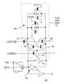
- FIG. 3is a schematic for a register file cell 300 having a state retentive memory in accordance with the present invention.
- Register file cell 300includes transistors 312 , 314 and 316 incorporated into a high performance section of an integrated circuit. Data is provided to transistor 314 , then transferred on the signal CLK by transistors 312 and 316 for storage on nodes 322 and 324 , where cross-coupled P-channel transistors 318 and 320 aid in writing the data. For low frequency operation, transistors 318 and 320 may be considered optional. Data stored on nodes 322 and 324 may be transferred through N-channel pass transistors 118 and 120 as controlled by the signal ACT 2 LOW for storage by inverters 130 and 132 in latch 128 .
- Register file cell 300further includes an N-channel transistor 326 having a gate connected to the input of inverter 130 and to the output of inverter 132 .
- N-channel transistor 328has a gate connected to the input of inverter 132 and to the output of inverter 130 .
- the sources of transistors 326 and 328are connected to a power conductor that receives a ground potential V SS .
- the signals CLK and DATAmay be referred to as WRITE_WORD_LINE and WRITE_BIT_LINE, respectively.
- FIG. 4is a schematic that provides a power supply scheme for register file cell 300 that is integrated with a processor core and a memory in a communications system.
- a power pin V CCreceives a voltage potential from an off-chip regulator that is supplied as an operating voltage potential to inverters 130 and 132 and to P-channel transistors 318 and 320 (see FIG. 3 ).
- transmission gate 410In normal operation (STANDBY is a zero logic value) transmission gate 410 is conducting, so that the voltage potential V CC supplied to the thin gate logic is substantially equivalent to the voltage potential V CCTG supplied to the thick gate logic in area 134 (see FIG. 3 ). With the voltage potentials V CC and V CCTG equivalent to one another, the P-channel transistors in N-well regions may be appropriately biased.
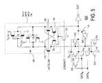
- FIG. 5is a schematic for a Set Dominant Latch (SDL) 500 having a state retentive memory in accordance with the present invention.
- the SDLis useful as a dynamic-to-static logic converter and since a logic state may be stored at dynamic nodes, the SDL may be used to properly restore the state to the thin gate logic.
- SDL 500receives input signals DATA A and DATA B at respective inputs of transistors 514 and 516 .
- the NAND function value of the input signals DATA A , DATA Bis resolved and available when the clock signal CLK is asserted. Note that one of transistors 514 or 516 may be optional so that SDL may be inverting rather than performing the Nand function.
- the signal ACT 2 LOWWhen entering a low power mode, the signal ACT 2 LOW may be asserted and the NAND function value may be transferred to latch 128 . With the NAND function value stored in latch 128 , the signal ACT 2 LOW may be deasserted and the operating voltage potential V CC that powers the NAND function logic and other logic in the high performance section may be switched to zero. The voltage potential of V CCTG is maintained high during the low power mode to keep inverters 130 and 132 powered. With the operating voltage potential V CC switched to zero, the gate leakage current of the thin gate-oxide transistors in the high performance section is negligible, thus providing lower power in a standby mode of operation.
- the signal LOW 2 ACTis asserted, followed by the operating voltage potential V CC being ramped to activate latch 110 .
- the state value retained in latch 128is written by transistors 122 , 124 and 126 back to inverter 524 and transistors 512 and 522 while powering up the high performance section.
- the signal LOW 2 ACTmay then be deasserted when the operating voltage potential V CC becomes stable.
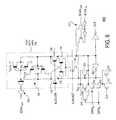
- FIG. 6is a schematic for a Set Dominant Latch (SDL) 600 having scan logic 510 , 520 and a state retentive memory in accordance with the present invention. Comparing FIGS. 5 and 6, additional gates have been added that allow SCAN IN data to be written into SDL 600 and the state value SCAN OUT to be passed on to another cell.
- scan logic 510shows SCAN IN data received in a scan mode and clocked by SCAN CKL for latching, with data transferred through N-channel pass transistors 118 and 120 as controlled by the signal ACT 2 LOW for storage by inverters 130 and 132 in latch 128 .
- Scan logic 520shows the state value SCAN OUT stored in latch 128 at an output of SDL 600 .
- FIG. 1Set Dominant Latch
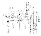
- FIG. 7is a schematic for a master/slave latch circuit 700 having scan and a state retentive memory in accordance with the present invention.
- the datais clocked by a signal CLK into a master portion 710 of the latch and transferred to a slave portion 712 when the signal CLK is deasserted.
- SCAN IN datamay be received by scan logic 714 in a scan mode and clocked by SCAN CLK for latching in slave portion 712 .
- Data stored in slave portion 712may be transferred through N-channel pass transistors 118 and 120 as controlled by the signal ACT 2 LOW for storage by inverters 130 and 132 in latch 128 .
- the signal ACT 2 LOWmay be deasserted and the operating voltage potential V CC that powers the master/slave and other logic in the high performance section may be switched to zero.
- the voltage potential of V CCTGis maintained high during the low power mode to keep inverters 130 and 132 powered. With the operating voltage potential V CC switched to zero, the gate leakage current of the thin gate-oxide transistors in the high performance section is negligible, thus providing lower power in a standby mode of operation.
- the signal LOW 2 ACTis asserted, followed by the operating voltage potential V CC being ramped to activate the master/slave.
- the data value retained in latch 128is written by transistors 122 , 124 and 126 back to slave portion 714 while powering up the high performance section.
- the signal LOW 2 ACTmay then be deasserted when the operating voltage potential V CC becomes stable. It is assumed that the master is open, i.e., the clock signal CLK is high, when powering up.
- FIG. 8is a schematic for a latch circuit 800 with scan and having a state retentive memory in accordance with the present invention.
- the datais clocked by a signal CLK into a latch 810 .
- SCAN IN datamay be received in a scan mode and clocked by SCAN CLK for writing scan data into latch 810 .
- the thick gate latchis used as the scan slave latch.
- Data stored in latch 810may be transferred through N-channel pass transistors 118 and 120 as controlled by the signal ACT 2 LOW for storage by inverters 130 and 132 in latch 128 .
- the signal ACT 2 LOWmay be deasserted and the operating voltage potential V CC that powers the latch 810 and other logic in the high performance section may be switched to zero.
- V CCTGThe voltage potential of V CCTG is maintained high during the low power mode to keep inverters 130 and 132 powered. With the operating voltage potential of the high performance section switched to zero, the gate leakage current of the thin gate-oxide transistors in that section is negligible, thus providing lower power in a standby mode of operation.
- the signal LOW 2 ACTis asserted, followed by the operating voltage potential of the high performance section being ramped to activate the latch 810 .
- the data value retained in latch 128is written by transistors 122 , 124 and 126 back to latch 810 while powering up the high performance section.
- the signal LOW 2 ACTmay then be deasserted when the operating voltage potential of the high performance section becomes stable.
- FIG. 9is a schematic for a latch 900 with scan and thin-gate scan slave latch in accordance with the present invention.
- the transistors in this embodiment that are used both in the high performance section and the state retentive memorymay be processed to have a thin gate-oxide thickness.
- the datais either clocked by a signal CLK, or alternatively, clocked by a signal SCAN CLK in a scan mode and for writing data into a latch 910 .
- Data stored in latch 910may be transferred through N-channel pass transistors 118 and 120 as controlled by the signal ACT 2 LOW for storage by inverters 130 and 132 in latch 128 .
- the signal ACT 2 LOWmay be deasserted and the operating voltage potential V CC that powers the latch 910 and other logic in the high performance section may be switched to zero.
- the voltage potential for inverters 136 and 132is not maintained high during the low power mode. This circuit demonstrates that a compatible non-state retentive scan scheme may be utilized for logic that does not require state retention.
Landscapes
- Engineering & Computer Science (AREA)
- Power Engineering (AREA)
- Logic Circuits (AREA)
- Static Random-Access Memory (AREA)
Abstract
Description
Claims (40)
Priority Applications (1)
| Application Number | Priority Date | Filing Date | Title |
|---|---|---|---|
| US10/329,124US6775180B2 (en) | 2002-12-23 | 2002-12-23 | Low power state retention |
Applications Claiming Priority (1)
| Application Number | Priority Date | Filing Date | Title |
|---|---|---|---|
| US10/329,124US6775180B2 (en) | 2002-12-23 | 2002-12-23 | Low power state retention |
Publications (2)
| Publication Number | Publication Date |
|---|---|
| US20040120182A1 US20040120182A1 (en) | 2004-06-24 |
| US6775180B2true US6775180B2 (en) | 2004-08-10 |
Family
ID=32594672
Family Applications (1)
| Application Number | Title | Priority Date | Filing Date |
|---|---|---|---|
| US10/329,124Expired - LifetimeUS6775180B2 (en) | 2002-12-23 | 2002-12-23 | Low power state retention |
Country Status (1)
| Country | Link |
|---|---|
| US (1) | US6775180B2 (en) |
Cited By (28)
| Publication number | Priority date | Publication date | Assignee | Title |
|---|---|---|---|---|
| US20050278559A1 (en)* | 2004-06-10 | 2005-12-15 | Marvell World Trade Ltd. | Low power computer with main and auxiliary processors |
| US20050289361A1 (en)* | 2004-06-10 | 2005-12-29 | Marvell World Trade Ltd. | Adaptive storage system |
| US20060104564A1 (en)* | 2004-11-15 | 2006-05-18 | Catrysse Peter B | Integrated waveguide and method for designing integrated waveguide |
| US20060145725A1 (en)* | 2004-12-31 | 2006-07-06 | Mccarroll David W | Relatively low standby power |
| US20060244493A1 (en)* | 2004-06-29 | 2006-11-02 | Schuelein Mark E | Ultra-drowsy circuit |
| US20060277360A1 (en)* | 2004-06-10 | 2006-12-07 | Sehat Sutardja | Adaptive storage system including hard disk drive with flash interface |
| US20070083785A1 (en)* | 2004-06-10 | 2007-04-12 | Sehat Sutardja | System with high power and low power processors and thread transfer |
| US20070094444A1 (en)* | 2004-06-10 | 2007-04-26 | Sehat Sutardja | System with high power and low power processors and thread transfer |
| US20070103201A1 (en)* | 2005-11-10 | 2007-05-10 | Lau Hon S | Power reducing logic and non-destructive latch circuits and applications |
| US20070121372A1 (en)* | 2005-11-25 | 2007-05-31 | Semiconductor Energy Laboratory Co., Ltd. | Semiconductor memory device and method for operating the same |
| US20070220202A1 (en)* | 2004-06-10 | 2007-09-20 | Sehat Sutardja | Adaptive storage system including hard disk drive with flash interface |
| US20070300131A1 (en)* | 2006-06-02 | 2007-12-27 | International Business Machines Corporation | Register file cell with soft error detection and circuits and methods using the cell |
| US20080123786A1 (en)* | 2006-11-29 | 2008-05-29 | Supat Wongwirawat | Method and apparatus for detecting and correcting modulated signal impairments |
| US20080140921A1 (en)* | 2004-06-10 | 2008-06-12 | Sehat Sutardja | Externally removable non-volatile semiconductor memory module for hard disk drives |
| US20080238510A1 (en)* | 2007-03-30 | 2008-10-02 | Aksamit Randy J | Low leakage state retention circuit |
| US20080288748A1 (en)* | 2006-08-10 | 2008-11-20 | Sehat Sutardja | Dynamic core switching |
| US7667498B1 (en) | 2004-12-31 | 2010-02-23 | Marvell International Ltd. | Relatively low standby power |
| US7788427B1 (en) | 2005-05-05 | 2010-08-31 | Marvell International Ltd. | Flash memory interface for disk drive |
| US7791389B2 (en) | 2008-01-30 | 2010-09-07 | Freescale Semiconductor, Inc. | State retaining power gated latch and method therefor |
| US7796445B1 (en) | 2007-02-12 | 2010-09-14 | Marvell International, Ltd. | State-retentive scan latch |
| US20110176653A1 (en)* | 2010-01-18 | 2011-07-21 | Stmicroelectronics S.R.L. | Low consumption flip-flop circuit with data retention and method thereof |
| US20120194105A1 (en)* | 2011-01-28 | 2012-08-02 | Kikuo Utsuno | Voltage determination device and clock control device |
| US8296703B1 (en) | 2008-12-19 | 2012-10-23 | Cadence Design Systems, Inc. | Fault modeling for state retention logic |
| US20120275236A1 (en)* | 2011-04-27 | 2012-11-01 | Hess Greg M | Method and Apparatus for Power Domain Isolation during Power Down |
| US20140009198A1 (en)* | 2012-07-06 | 2014-01-09 | Semiconductor Energy Laboratory Co., Ltd. | Semiconductor device and method of driving semiconductor device |
| US10222421B1 (en) | 2018-02-14 | 2019-03-05 | Silicon Laboratories Inc. | Method for detecting faults on retention cell pins |
| US11988720B2 (en) | 2018-12-20 | 2024-05-21 | Semiconductor Energy Laboratory Co., Ltd. | Semiconductor device and battery pack |
| US12132334B2 (en) | 2018-11-22 | 2024-10-29 | Semiconductor Energy Laboratory Co., Ltd. | Semiconductor device and battery pack |
Families Citing this family (6)
| Publication number | Priority date | Publication date | Assignee | Title |
|---|---|---|---|---|
| US7200068B2 (en)* | 2002-12-27 | 2007-04-03 | Intel Corporation | Multi-ported register files |
| DE102004055006B4 (en)* | 2004-11-15 | 2012-09-13 | Infineon Technologies Ag | Flip-flop with additional state storage at shutdown |
| US7908500B2 (en)* | 2007-10-01 | 2011-03-15 | Silicon Laboratories Inc. | Low power retention flip-flops |
| US20110304306A1 (en)* | 2010-06-09 | 2011-12-15 | Intel Corporation | Current mode control of voltage regulators to mitigate output voltage ripple |
| US9590634B1 (en)* | 2016-06-13 | 2017-03-07 | Baysand Inc. | Metal configurable hybrid memory |
| US10734978B2 (en)* | 2018-12-28 | 2020-08-04 | Texas Instruments Incorporated | Enhanced immunity latched logic state retention |
Citations (1)
| Publication number | Priority date | Publication date | Assignee | Title |
|---|---|---|---|---|
| US6639827B2 (en)* | 2002-03-12 | 2003-10-28 | Intel Corporation | Low standby power using shadow storage |
- 2002
- 2002-12-23USUS10/329,124patent/US6775180B2/ennot_activeExpired - Lifetime
Patent Citations (1)
| Publication number | Priority date | Publication date | Assignee | Title |
|---|---|---|---|---|
| US6639827B2 (en)* | 2002-03-12 | 2003-10-28 | Intel Corporation | Low standby power using shadow storage |
Cited By (59)
| Publication number | Priority date | Publication date | Assignee | Title |
|---|---|---|---|---|
| US20080140921A1 (en)* | 2004-06-10 | 2008-06-12 | Sehat Sutardja | Externally removable non-volatile semiconductor memory module for hard disk drives |
| US20070220202A1 (en)* | 2004-06-10 | 2007-09-20 | Sehat Sutardja | Adaptive storage system including hard disk drive with flash interface |
| US7617359B2 (en) | 2004-06-10 | 2009-11-10 | Marvell World Trade Ltd. | Adaptive storage system including hard disk drive with flash interface |
| US7636809B2 (en) | 2004-06-10 | 2009-12-22 | Marvell World Trade Ltd. | Adaptive storage system including hard disk drive with flash interface |
| US7512734B2 (en) | 2004-06-10 | 2009-03-31 | Marvell International Ltd. | Adaptive storage system |
| US20060277360A1 (en)* | 2004-06-10 | 2006-12-07 | Sehat Sutardja | Adaptive storage system including hard disk drive with flash interface |
| US20070083785A1 (en)* | 2004-06-10 | 2007-04-12 | Sehat Sutardja | System with high power and low power processors and thread transfer |
| US20070094444A1 (en)* | 2004-06-10 | 2007-04-26 | Sehat Sutardja | System with high power and low power processors and thread transfer |
| US7827423B2 (en) | 2004-06-10 | 2010-11-02 | Marvell World Trade Ltd. | Low power computer with main and auxiliary processors |
| US20070226409A1 (en)* | 2004-06-10 | 2007-09-27 | Sehat Sutardja | Adaptive storage system including hard disk drive with flash interface |
| US20050289361A1 (en)* | 2004-06-10 | 2005-12-29 | Marvell World Trade Ltd. | Adaptive storage system |
| US8572416B2 (en) | 2004-06-10 | 2013-10-29 | Marvell World Trade Ltd. | Low power computer with main and auxiliary processors |
| US7634615B2 (en) | 2004-06-10 | 2009-12-15 | Marvell World Trade Ltd. | Adaptive storage system |
| US20050278559A1 (en)* | 2004-06-10 | 2005-12-15 | Marvell World Trade Ltd. | Low power computer with main and auxiliary processors |
| US7702848B2 (en) | 2004-06-10 | 2010-04-20 | Marvell World Trade Ltd. | Adaptive storage system including hard disk drive with flash interface |
| US7788514B2 (en) | 2004-06-10 | 2010-08-31 | Marvell World Trade Ltd. | Low power computer with main and auxiliary processors |
| US20080222437A1 (en)* | 2004-06-10 | 2008-09-11 | Sehat Sutardja | Low power computer with main and auxiliary processors |
| US8874948B2 (en) | 2004-06-10 | 2014-10-28 | Marvell World Trade Ltd. | Apparatuses for operating, during respective power modes, transistors of multiple processors at corresponding duty cycles |
| US7730335B2 (en) | 2004-06-10 | 2010-06-01 | Marvell World Trade Ltd. | Low power computer with main and auxiliary processors |
| US7236032B2 (en)* | 2004-06-29 | 2007-06-26 | Intel Corporation | Ultra-drowsy circuit |
| US20060244493A1 (en)* | 2004-06-29 | 2006-11-02 | Schuelein Mark E | Ultra-drowsy circuit |
| US20060104564A1 (en)* | 2004-11-15 | 2006-05-18 | Catrysse Peter B | Integrated waveguide and method for designing integrated waveguide |
| US8076956B1 (en) | 2004-12-31 | 2011-12-13 | Marvell International Ltd. | Relatively low standby power |
| US7443205B2 (en) | 2004-12-31 | 2008-10-28 | Marvell International Ltd. | Relatively low standby power |
| US20060145725A1 (en)* | 2004-12-31 | 2006-07-06 | Mccarroll David W | Relatively low standby power |
| US7667498B1 (en) | 2004-12-31 | 2010-02-23 | Marvell International Ltd. | Relatively low standby power |
| US7788427B1 (en) | 2005-05-05 | 2010-08-31 | Marvell International Ltd. | Flash memory interface for disk drive |
| US7979614B1 (en) | 2005-05-05 | 2011-07-12 | Marvell International Ltd. | Flash memory/disk drive interface and method for same |
| US20070103201A1 (en)* | 2005-11-10 | 2007-05-10 | Lau Hon S | Power reducing logic and non-destructive latch circuits and applications |
| US8305112B2 (en) | 2005-11-10 | 2012-11-06 | Intel Corporation | Power reducing logic and non-destructive latch circuits and applications |
| US8421502B2 (en) | 2005-11-10 | 2013-04-16 | Intel Corporation | Power reducing logic and non-destructive latch circuits and applications |
| US9490807B2 (en) | 2005-11-10 | 2016-11-08 | Intel Corporation | Power reducing logic and non-destructive latch circuits and applications |
| US20100289528A1 (en)* | 2005-11-10 | 2010-11-18 | Hon Shing Lau | Power reducing logic and non-destructive latch circuits and applications |
| US7613030B2 (en)* | 2005-11-25 | 2009-11-03 | Semiconductor Energy Laboratory Co., Ltd. | Semiconductor memory device and method for operating the same |
| US20070121372A1 (en)* | 2005-11-25 | 2007-05-31 | Semiconductor Energy Laboratory Co., Ltd. | Semiconductor memory device and method for operating the same |
| US20070300131A1 (en)* | 2006-06-02 | 2007-12-27 | International Business Machines Corporation | Register file cell with soft error detection and circuits and methods using the cell |
| US7562273B2 (en)* | 2006-06-02 | 2009-07-14 | International Business Machines Corporation | Register file cell with soft error detection and circuits and methods using the cell |
| CN101083131B (en)* | 2006-06-02 | 2011-12-21 | 国际商业机器公司 | Register file cell and circuits and methods for operating register file circuit |
| US9158355B2 (en) | 2006-08-10 | 2015-10-13 | Marvell World Trade Ltd. | Dynamic core switching |
| US20080288748A1 (en)* | 2006-08-10 | 2008-11-20 | Sehat Sutardja | Dynamic core switching |
| US20080123786A1 (en)* | 2006-11-29 | 2008-05-29 | Supat Wongwirawat | Method and apparatus for detecting and correcting modulated signal impairments |
| US7796445B1 (en) | 2007-02-12 | 2010-09-14 | Marvell International, Ltd. | State-retentive scan latch |
| US20080238510A1 (en)* | 2007-03-30 | 2008-10-02 | Aksamit Randy J | Low leakage state retention circuit |
| US7626434B2 (en) | 2007-03-30 | 2009-12-01 | Intel Corporation | Low leakage state retention circuit |
| US7791389B2 (en) | 2008-01-30 | 2010-09-07 | Freescale Semiconductor, Inc. | State retaining power gated latch and method therefor |
| US8296703B1 (en) | 2008-12-19 | 2012-10-23 | Cadence Design Systems, Inc. | Fault modeling for state retention logic |
| US20110176653A1 (en)* | 2010-01-18 | 2011-07-21 | Stmicroelectronics S.R.L. | Low consumption flip-flop circuit with data retention and method thereof |
| US8570085B2 (en) | 2010-01-18 | 2013-10-29 | Stmicroelectronics S.R.L. | Low consumption flip-flop circuit with data retention and method thereof |
| US8330518B2 (en)* | 2010-01-18 | 2012-12-11 | Stmicroelectronics S.R.L. | Low consumption flip-flop circuit with data retention and method thereof |
| US8610381B2 (en)* | 2011-01-28 | 2013-12-17 | Lapis Semiconductor Co., Ltd. | Voltage determination device and clock control device |
| US20120194105A1 (en)* | 2011-01-28 | 2012-08-02 | Kikuo Utsuno | Voltage determination device and clock control device |
| US9223335B2 (en) | 2011-01-28 | 2015-12-29 | Lapis Semiconductor Co., Ltd. | Semiconductor device |
| US20120275236A1 (en)* | 2011-04-27 | 2012-11-01 | Hess Greg M | Method and Apparatus for Power Domain Isolation during Power Down |
| US8570788B2 (en)* | 2011-04-27 | 2013-10-29 | Apple Inc. | Method and apparatus for power domain isolation during power down |
| US20140009198A1 (en)* | 2012-07-06 | 2014-01-09 | Semiconductor Energy Laboratory Co., Ltd. | Semiconductor device and method of driving semiconductor device |
| US9083327B2 (en)* | 2012-07-06 | 2015-07-14 | Semiconductor Energy Laboratory Co., Ltd. | Semiconductor device and method of driving semiconductor device |
| US10222421B1 (en) | 2018-02-14 | 2019-03-05 | Silicon Laboratories Inc. | Method for detecting faults on retention cell pins |
| US12132334B2 (en) | 2018-11-22 | 2024-10-29 | Semiconductor Energy Laboratory Co., Ltd. | Semiconductor device and battery pack |
| US11988720B2 (en) | 2018-12-20 | 2024-05-21 | Semiconductor Energy Laboratory Co., Ltd. | Semiconductor device and battery pack |
Also Published As
| Publication number | Publication date |
|---|---|
| US20040120182A1 (en) | 2004-06-24 |
Similar Documents
| Publication | Publication Date | Title |
|---|---|---|
| US6775180B2 (en) | Low power state retention | |
| US6774696B2 (en) | Level shifter and voltage translator | |
| US6639827B2 (en) | Low standby power using shadow storage | |
| Shigematsu et al. | A 1-V high-speed MTCMOS circuit scheme for power-down application circuits | |
| US7577858B2 (en) | Method for reducing power consumption in a state retaining circuit, state retaining circuit and electronic device | |
| US5867040A (en) | Integrated circuit with stacked sub-circuits between Vcc and ground so as to conserve power and reduce the voltage across any one transistor | |
| US6677797B2 (en) | Semiconductor integrated circuit | |
| KR100632138B1 (en) | Low voltage operation of static random access memory | |
| JPH11112297A (en) | Latch circuit and semiconductor integrated circuit having the same | |
| US6759873B2 (en) | Reverse biasing logic circuit | |
| US5703825A (en) | Semiconductor integrated circuit device having a leakage current reduction means | |
| Sridhara et al. | Subthreshold leakage power reduction in VLSI circuits: A survey | |
| US6385099B1 (en) | Reducing level shifter standby power consumption | |
| US8589711B1 (en) | Power supply delivery for leakage suppression modes | |
| TWI719848B (en) | Reference voltage holding circuit and sense amplifier circuit having reference voltage holding circuit | |
| US6617916B1 (en) | Semiconductor integrated circuit | |
| JP2005516454A (en) | Integrated circuit and battery-powered electronic device | |
| KR19980022291A (en) | Internal voltage converter of semiconductor memory device and driving method thereof | |
| Aich et al. | Comparison of Techniques for Reducing Leakage Current in SRAM: A Study of Gated V DD, MTCMOS, and Clamping Diode Techniques | |
| US7667498B1 (en) | Relatively low standby power | |
| US7443205B2 (en) | Relatively low standby power | |
| US6549037B1 (en) | Apparatus and circuit having reduced leakage current and method therefor | |
| Yim et al. | Single-Ended Back-Bias Voltage Generator Using One Pumping Capacitor | |
| KR100284290B1 (en) | Standby Current Reduction Circuit Using Substrate Voltage | |
| Pacha et al. | Leakage Reduction in Sub-100nm CMOS Technologies: Bridging the Gap Between Technology, Circuit Design and Low Power Product Requirements |
Legal Events
| Date | Code | Title | Description |
|---|---|---|---|
| AS | Assignment | Owner name:INTEL CORPORATION, CALIFORNIA Free format text:ASSIGNMENT OF ASSIGNORS INTEREST;ASSIGNORS:BIYANI, MANISH;CLARK, LAWRENCE T.;DEMMONS, SHAY P.;AND OTHERS;REEL/FRAME:013968/0898;SIGNING DATES FROM 20030203 TO 20030214 | |
| STCF | Information on status: patent grant | Free format text:PATENTED CASE | |
| FEPP | Fee payment procedure | Free format text:PAYOR NUMBER ASSIGNED (ORIGINAL EVENT CODE: ASPN); ENTITY STATUS OF PATENT OWNER: LARGE ENTITY | |
| CC | Certificate of correction | ||
| AS | Assignment | Owner name:MARVELL INTERNATIONAL LTD.,BERMUDA Free format text:ASSIGNMENT OF ASSIGNORS INTEREST;ASSIGNOR:INTEL CORPORATION;REEL/FRAME:018515/0817 Effective date:20061108 Owner name:MARVELL INTERNATIONAL LTD., BERMUDA Free format text:ASSIGNMENT OF ASSIGNORS INTEREST;ASSIGNOR:INTEL CORPORATION;REEL/FRAME:018515/0817 Effective date:20061108 | |
| FEPP | Fee payment procedure | Free format text:PAYER NUMBER DE-ASSIGNED (ORIGINAL EVENT CODE: RMPN); ENTITY STATUS OF PATENT OWNER: LARGE ENTITY Free format text:PAYOR NUMBER ASSIGNED (ORIGINAL EVENT CODE: ASPN); ENTITY STATUS OF PATENT OWNER: LARGE ENTITY | |
| FPAY | Fee payment | Year of fee payment:4 | |
| REMI | Maintenance fee reminder mailed | ||
| FPAY | Fee payment | Year of fee payment:8 | |
| FPAY | Fee payment | Year of fee payment:12 | |
| AS | Assignment | Owner name:CAVIUM INTERNATIONAL, CAYMAN ISLANDS Free format text:ASSIGNMENT OF ASSIGNORS INTEREST;ASSIGNOR:MARVELL INTERNATIONAL LTD.;REEL/FRAME:052918/0001 Effective date:20191231 | |
| AS | Assignment | Owner name:MARVELL ASIA PTE, LTD., SINGAPORE Free format text:ASSIGNMENT OF ASSIGNORS INTEREST;ASSIGNOR:CAVIUM INTERNATIONAL;REEL/FRAME:053475/0001 Effective date:20191231 |