US6774865B1 - Portable electronic device comprising several contact-free integrated circuits - Google Patents
Portable electronic device comprising several contact-free integrated circuitsDownload PDFInfo
- Publication number
- US6774865B1 US6774865B1US10/338,339US33833903AUS6774865B1US 6774865 B1US6774865 B1US 6774865B1US 33833903 AUS33833903 AUS 33833903AUS 6774865 B1US6774865 B1US 6774865B1
- Authority
- US
- United States
- Prior art keywords
- coil
- integrated circuit
- integrated circuits
- collective
- individual
- Prior art date
- Legal status (The legal status is an assumption and is not a legal conclusion. Google has not performed a legal analysis and makes no representation as to the accuracy of the status listed.)
- Expired - Lifetime
Links
Images


Classifications
- G—PHYSICS
- G06—COMPUTING OR CALCULATING; COUNTING
- G06K—GRAPHICAL DATA READING; PRESENTATION OF DATA; RECORD CARRIERS; HANDLING RECORD CARRIERS
- G06K19/00—Record carriers for use with machines and with at least a part designed to carry digital markings
- G06K19/06—Record carriers for use with machines and with at least a part designed to carry digital markings characterised by the kind of the digital marking, e.g. shape, nature, code
- G06K19/067—Record carriers with conductive marks, printed circuits or semiconductor circuit elements, e.g. credit or identity cards also with resonating or responding marks without active components
- G06K19/07—Record carriers with conductive marks, printed circuits or semiconductor circuit elements, e.g. credit or identity cards also with resonating or responding marks without active components with integrated circuit chips
- G06K19/077—Constructional details, e.g. mounting of circuits in the carrier
- G06K19/07749—Constructional details, e.g. mounting of circuits in the carrier the record carrier being capable of non-contact communication, e.g. constructional details of the antenna of a non-contact smart card
- G06K19/07758—Constructional details, e.g. mounting of circuits in the carrier the record carrier being capable of non-contact communication, e.g. constructional details of the antenna of a non-contact smart card arrangements for adhering the record carrier to further objects or living beings, functioning as an identification tag
- G—PHYSICS
- G06—COMPUTING OR CALCULATING; COUNTING
- G06K—GRAPHICAL DATA READING; PRESENTATION OF DATA; RECORD CARRIERS; HANDLING RECORD CARRIERS
- G06K19/00—Record carriers for use with machines and with at least a part designed to carry digital markings
- G06K19/06—Record carriers for use with machines and with at least a part designed to carry digital markings characterised by the kind of the digital marking, e.g. shape, nature, code
- G06K19/067—Record carriers with conductive marks, printed circuits or semiconductor circuit elements, e.g. credit or identity cards also with resonating or responding marks without active components
- G06K19/07—Record carriers with conductive marks, printed circuits or semiconductor circuit elements, e.g. credit or identity cards also with resonating or responding marks without active components with integrated circuit chips
- G06K19/072—Record carriers with conductive marks, printed circuits or semiconductor circuit elements, e.g. credit or identity cards also with resonating or responding marks without active components with integrated circuit chips the record carrier comprising a plurality of integrated circuit chips
- G—PHYSICS
- G06—COMPUTING OR CALCULATING; COUNTING
- G06K—GRAPHICAL DATA READING; PRESENTATION OF DATA; RECORD CARRIERS; HANDLING RECORD CARRIERS
- G06K19/00—Record carriers for use with machines and with at least a part designed to carry digital markings
- G06K19/06—Record carriers for use with machines and with at least a part designed to carry digital markings characterised by the kind of the digital marking, e.g. shape, nature, code
- G06K19/067—Record carriers with conductive marks, printed circuits or semiconductor circuit elements, e.g. credit or identity cards also with resonating or responding marks without active components
- G06K19/07—Record carriers with conductive marks, printed circuits or semiconductor circuit elements, e.g. credit or identity cards also with resonating or responding marks without active components with integrated circuit chips
- G06K19/0723—Record carriers with conductive marks, printed circuits or semiconductor circuit elements, e.g. credit or identity cards also with resonating or responding marks without active components with integrated circuit chips the record carrier comprising an arrangement for non-contact communication, e.g. wireless communication circuits on transponder cards, non-contact smart cards or RFIDs
- G—PHYSICS
- G06—COMPUTING OR CALCULATING; COUNTING
- G06K—GRAPHICAL DATA READING; PRESENTATION OF DATA; RECORD CARRIERS; HANDLING RECORD CARRIERS
- G06K19/00—Record carriers for use with machines and with at least a part designed to carry digital markings
- G06K19/06—Record carriers for use with machines and with at least a part designed to carry digital markings characterised by the kind of the digital marking, e.g. shape, nature, code
- G06K19/067—Record carriers with conductive marks, printed circuits or semiconductor circuit elements, e.g. credit or identity cards also with resonating or responding marks without active components
- G06K19/07—Record carriers with conductive marks, printed circuits or semiconductor circuit elements, e.g. credit or identity cards also with resonating or responding marks without active components with integrated circuit chips
- G06K19/077—Constructional details, e.g. mounting of circuits in the carrier
- G06K19/07749—Constructional details, e.g. mounting of circuits in the carrier the record carrier being capable of non-contact communication, e.g. constructional details of the antenna of a non-contact smart card
- G06K19/0775—Constructional details, e.g. mounting of circuits in the carrier the record carrier being capable of non-contact communication, e.g. constructional details of the antenna of a non-contact smart card arrangements for connecting the integrated circuit to the antenna
- G06K19/07756—Constructional details, e.g. mounting of circuits in the carrier the record carrier being capable of non-contact communication, e.g. constructional details of the antenna of a non-contact smart card arrangements for connecting the integrated circuit to the antenna the connection being non-galvanic, e.g. capacitive
- G—PHYSICS
- G06—COMPUTING OR CALCULATING; COUNTING
- G06K—GRAPHICAL DATA READING; PRESENTATION OF DATA; RECORD CARRIERS; HANDLING RECORD CARRIERS
- G06K19/00—Record carriers for use with machines and with at least a part designed to carry digital markings
- G06K19/06—Record carriers for use with machines and with at least a part designed to carry digital markings characterised by the kind of the digital marking, e.g. shape, nature, code
- G06K19/067—Record carriers with conductive marks, printed circuits or semiconductor circuit elements, e.g. credit or identity cards also with resonating or responding marks without active components
- G06K19/07—Record carriers with conductive marks, printed circuits or semiconductor circuit elements, e.g. credit or identity cards also with resonating or responding marks without active components with integrated circuit chips
- G06K19/077—Constructional details, e.g. mounting of circuits in the carrier
- G06K19/07749—Constructional details, e.g. mounting of circuits in the carrier the record carrier being capable of non-contact communication, e.g. constructional details of the antenna of a non-contact smart card
- G06K19/07796—Constructional details, e.g. mounting of circuits in the carrier the record carrier being capable of non-contact communication, e.g. constructional details of the antenna of a non-contact smart card arrangements on the record carrier to allow stacking of a plurality of similar record carriers, e.g. to avoid interference between the non-contact communication of the plurality of record carriers
- G—PHYSICS
- G06—COMPUTING OR CALCULATING; COUNTING
- G06K—GRAPHICAL DATA READING; PRESENTATION OF DATA; RECORD CARRIERS; HANDLING RECORD CARRIERS
- G06K7/00—Methods or arrangements for sensing record carriers, e.g. for reading patterns
- G06K7/10—Methods or arrangements for sensing record carriers, e.g. for reading patterns by electromagnetic radiation, e.g. optical sensing; by corpuscular radiation
- G06K7/10009—Methods or arrangements for sensing record carriers, e.g. for reading patterns by electromagnetic radiation, e.g. optical sensing; by corpuscular radiation sensing by radiation using wavelengths larger than 0.1 mm, e.g. radio-waves or microwaves
- G06K7/10158—Methods or arrangements for sensing record carriers, e.g. for reading patterns by electromagnetic radiation, e.g. optical sensing; by corpuscular radiation sensing by radiation using wavelengths larger than 0.1 mm, e.g. radio-waves or microwaves methods and means used by the interrogation device for reliably powering the wireless record carriers using an electromagnetic interrogation field
- G06K7/10178—Methods or arrangements for sensing record carriers, e.g. for reading patterns by electromagnetic radiation, e.g. optical sensing; by corpuscular radiation sensing by radiation using wavelengths larger than 0.1 mm, e.g. radio-waves or microwaves methods and means used by the interrogation device for reliably powering the wireless record carriers using an electromagnetic interrogation field including auxiliary means for focusing, repeating or boosting the electromagnetic interrogation field
Definitions
- the present inventionrelates to contactless integrated circuits and portable electronic devices produced by means of these integrated circuits.
- FIG. 1is a very schematic representation of a contactless integrated circuit 1 connected to an antenna coil 2 .
- the integrated circuit 1is active when coil 2 is dipped into a magnetic field FLD sent by a data send/receive station 5 which itself comprises, for that purpose, an antenna coil 6 .
- the magnetic field FLD sent by the station 5oscillates at a determined frequency, such as 13.56 MHz for example, according to ISO 14443 standard.
- data transmission DTr from the station 5 to the integrated circuit 1is carried out by modulating the amplitude of the antenna signal, with a 100% (ISO 14443/A) or 10% (ISO 14443/B) depth of modulation for example.
- Data transmission DTx from the integrated circuit 1 to the station 5is carried out by modulating the coil 2 load.
- the load modulation signalis passed on by inductive coupling in the coil 6 of the station 2 wherein it is filtered and decoded to retrieve the data DTx that it contains.
- One ideawhich represents in itself one aspect of the present invention, is to produce a portable electronic device comprising a combination of contactless integrated circuits.
- the present inventionis based on the consideration according to which a combination of several contactless integrated circuits is capable of offering various advantages and to be used in various applications, as demonstrated below.
- a devicecomprising several contactless integrated circuits must be compact and offer a maximum distance of communication with each of the integrated circuits which is not too short.
- Maximum distance of communicationshall mean the distance of communication above which no data transmission is possible, due to too low inductive coupling.
- a simple juxtaposition of contactless integrated circuits each equipped with an antenna coildoes not enable a satisfactory compromise to be found between minimum overall dimensions of the device and a satisfactory maximum distance of communication, pursuant to the principle according to which the maximum distance of communication increases in proportion to the size of the antenna coil.
- the juxtaposition of several small micromodules incorporating a contactless integrated circuit and an antenna small in sizeleads to produce a device the size of which is satisfactory, but wherein each micromodule offers a short maximum distance of communication.
- the juxtaposition of several modules each incorporating a contactless integrated circuit and an antenna of large diameterleads to produce a device offering a satisfactory maximum distance of communication but having considerable overall dimensions and a significant cost price due to the cost of manufacturing each antenna and of the raw material used.
- the present inventionaims to provide a device comprising a combination of contactless integrated circuits which have reduced overall dimensions while offering a satisfactory maximum distance of communication.
- a devicecomprising a combination of at least two contactless integrated circuits, each integrated circuit being connected to an individual antenna coil to send and/or receive data by inductive coupling, the device comprising a collective antenna coil that is larger in size than the individual antenna coils of the integrated circuits, and means for arranging the individual coil of an integrated circuit proximate to the collective coil, at least when data are to be read and/or written in the integrated circuit, so that the individual coil of the integrated circuit is inductively coupled to the collective coil, the integrated circuits being arranged or programmed to implement an anti-collision protocol which enables a data send and/or receive station to select one, and only one, integrated circuit during communication with the device.
- the individual coil of each integrated circuitis permanently coupled to the collective coil.
- the collective coil, the integrated circuits and the individual antenna coilsare arranged on a common support, the integrated circuits and the individual antenna coils being placed in the centre of the collective coil.
- the collective coilis arranged on a first support
- the integrated circuitsare arranged on one or more supports which are different from the first support
- the devicecomprising means for moving the support of an integrated circuit closer to the support of the collective coil at least when data are to be read and/or written in the integrated circuit.
- the collective coil and the integrated circuitsare arranged on substantially flat supports structured around an axis so as to form a sort of notebook.
- the flat supportsare jackets.
- each integrated circuit and its individual antenna coilare produced in the form of a small micromodule.
- the integrated circuitsare arranged or programmed to form together an equivalent integrated circuit the total data storage capacity of which is greater than the individual storage capacity of each integrated circuit.
- each integrated circuitcomprises a datum in its memory representing the rank of the integrated circuit with regard to the other integrated circuits of the device, with a view to adding the data storage capacities of the integrated circuits by adding storage areas.
- FIG. 1 described aboveis a schematic representation of a contactless integrated circuit and a data send/receive station
- FIG. 2is a schematic representation of a classical, contactless smart card of a first type
- FIG. 3is a schematic representation of a classical, contactless smart card of a second type
- FIG. 4represents a classical, contactless electronic micromodule of a first type
- FIG. 5represents a classical, contactless electronic micromodule of a second type
- FIG. 6represents a classical, contactless electronic micromodule of a third type
- FIG. 7represents a classical arrangement of contactless integrated circuits wherein the implementation of an anti-collision method is required
- FIG. 8represents a first example of an embodiment of a device according to the present invention.
- FIG. 9represents, by a lateral view, a second example of an embodiment of a device according to the present invention.
- FIG. 10is a front view of the device in FIG. 9, and
- FIG. 11is a diagram representing a classical architecture of a contactless integrated circuit.
- the simple juxtaposition of a set of contactless integrated circuits each equipped with an antenna coildoes not enable a satisfactory compromise to be found between minimum overall dimensions and a satisfactory distance of communication with each of the integrated circuits.
- FIGS. 2 to 6represent various classical embodiments of contactless electronic modules, and illustrate the technical problem that the present invention aims to resolve.
- FIGS. 2 and 3represent contactless modules of the smart card type having an extensive maximum distance of communication, which can reach several tens of centimeters, but with considerable overall dimensions.
- FIGS. 4 to 6represent contactless micromodules with small overall dimensions, but offering a reduced maximum distance of communication, in the order of one millimeter to a few centimeters according to the micromodule considered.
- the values of maximum distance of communication mentionedare only relative and are based on experimental findings made under normal conditions of inductive coupling, particularly power consumption by the antenna of a data send/receive station in the order of a few Watts.
- Module 10 represented in FIG. 2is a contactless smart card or an electronic badge made up of a rectangular plastic support 11 on which (or wherein) a contactless integrated circuit 1 and its antenna coil 12 are arranged.
- the coil 12travels through the periphery of the support 11 in one or more turns and offers a substantial maximum distance of communication, in the order of about ten centimeters to some tens of centimeters, and even to one or two meters with a powerful reader.
- FIG. 3is a variation 15 of the contactless card in FIG. 2 which differs from the latter in that the support 11 comprises a larger antenna coil 16 , which is equivalent to the coil 12 in FIG. 2, and a small antenna coil 17 .
- the integrated circuit 1 and the small coil 17are arranged in the centre of the coil 16 , the coil 17 being connected to the integrated circuit 1 , whereas the large coil 16 is in closed loop, its two extremities being connected together.
- the large coil 16 and the small coil 17are inductively coupled and the large coil 16 forms a sort of passive relay amplifier for the small coil 17 .
- the inductive coupling between both coilsis reinforced by providing a turn 16 - 1 of the large coil 16 which surrounds the small coil 17 at a short distance from the latter.
- a contactless smart card produced in accordance with FIG. 3is deemed to be less costly to manufacture than the contactless smart card represented in FIG. 2, as there is no electrical contact to be implemented between the large coil 16 and the integrated circuit 1 when manufacturing the card.
- the integrated circuit 1 and the small coil 17may be produced in the form of an integrated micromodule, according to collective manufacturing techniques the implementation of which is not costly.
- the micromodule 20 in FIG. 4comprises an epoxy or ceramic support wafer 21 that is smaller than the plastic support described above and which carries a contactless integrated circuit 1 and an antenna coil 22 .
- the coil 22closely surrounds the silicon wafer of the integrated circuit 1 and the surface of the assembly can be reduced to a few square centimeters.
- the overall dimensions of the micromodule 20are clearly less than those of a smart card but the maximum distance of communication offered is shorter, in the order of one centimeter to a few centimeters.
- the micromodule 25 in FIG. 5is produced according to the so-called “coil on chip” technique and is exclusively made up of the silicon wafer of the integrated circuit 1 , a coil 26 being directly formed on the silicon wafer by plating.
- the active area of the waferwhich comprises the electronic components of the integrated circuit, is represented by a hatched area. This active area may be arranged in the center of the coil 26 , as represented, or be completely covered with the coil 26 .
- This type of micromodulerepresents, at the present time, the highest degree of integration of a contactless integrated circuit and its associated coil but offers a maximum distance of communication that is very short, in the order of one millimeter to a few millimeters.
- the micromodule 30comprises a support wafer 31 , made of silicon for example, on which the contactless integrated circuit 1 is arranged.
- the integrated circuit 1is buried in an insulating layer (not visible on the Figure), made of polyimide for example, on which a coil 32 is arranged, and openings are made in the insulating layer to ensure an electrical contact between the integrated circuit and the coil.
- the micromodule 30has larger overall dimensions than the one in FIG. 5 but clearly less than the one in FIG. 4 .
- the support 31offers a surface for arranging the coil which is larger than that of the wafer of the integrated circuit 1 , the size of the coil 32 can be chosen larger and the maximum distance of communication obtained can be in the order of that of the micromodule in FIG. 4, for overall dimensions which are smaller.
- the present inventionis based on the simple, but no less inventive, idea according to which the amplification technique of the inductive coupling by means of an antenna coil arranged in closed loop, as illustrated in FIG. 3, is applicable to the production of a device comprising several integrated circuits and their individual antenna coils, the amplifier passive coil being used, in this case, as a collective antenna. As indicated in FIG. 3, there is, indeed, in the centre of the coil substantial room that can be used to receive other integrated circuits and their individual coils.
- Another idea of the present inventionwhich goes hand in hand with the first one, is to provide means for managing collisions between messages in each integrated circuit. These collisions will inevitably occur since contactless integrated circuits sharing the same collective antenna coil will be simultaneously activated by the magnetic field sent by a data send/receive station.
- FIG. 7illustrates a classical case of collision between three contactless integrated circuits 1 , 1 ′, 1 ′′ each fitted with an antenna coil 2 , 2 ′, 2 ′′ and located simultaneously in the interrogation field FLD sent by a data send and/or receive station 5 .
- One, and only one, integrated circuitmust be selected by the station 5 and the others must go into standby mode for the duration of the communication.
- various methods called “anti-collision” methodsmay be used, particularly the one described by ISO 14443 standard or in the international application WO 97/42578 in the name of the applicant.
- This anti-collision methodincludes for example sending a general interrogation message to the integrated circuits, and selecting the integrated circuit that has answered first.
- the integrated circuitsare arranged in order to, upon receiving an interrogation message, determine a random response position on a response time scale, send a response message when the response position has been reached or go into standby mode when a message is received before the response position has been reached.
- FIG. 8represents a device according to the present invention 40 , comprising a support 41 on which (or wherein) a collective coil 42 arranged in closed loop is arranged (is incorporated).
- the support 41is made of plastic, epoxy or ceramic for example, and the collective coil 42 is made of copper, aluminium or by means of electrically conductive ink.
- micromodules 45here four micromodules 45 , 45 ′, 45 ′′, 45 ′′′, are arranged in the centre of the collective coil 42 .
- the “centre of the collective coil”is an area that is demarcated by the smallest winding in diameter of the collective coil.
- the micromodules 45represented in a simplified manner, each comprise a contactless integrated circuit and an individual antenna coil 46 , 46 ′, 46 ′′, 46 ′′′ that is small in size.
- the micromodulesare produced according to any known manufacturing technique, particularly one of the techniques previously described in relation with FIGS. 4, 5 and 6 .
- a micromodule 45 produced in accordance with micromodule 25 in FIG. 5is a simple silicon chip on which a coil has previously been formed.
- Each micromodule 45implements a data transmission protocol incorporating an anti-collision method of the type described above.
- each micromodule 45is inductively coupled to the collective coil 42 due to the arrangement of the micromodules in the centre of the collective coil 42 .
- the maximum distance of communication with each micromodule 45is satisfactory and is in the order of ten times the maximum distance of communication that each micromodule would have in the absence of the collective coil 42 .
- the device 40is susceptible of various variations, particularly as far as the shape of the support and of the collective antenna is concerned, as well as their constituent materials.
- the collective coil 42may have various windings with small diameters in its centre which surround the micromodules 45 , just like winding 16 - 1 represented in FIG. 3 .
- the device 40is also susceptible of various applications.
- the device 40is used as an electronic label for the identification of goods, each integrated circuit being assigned to the storage of a determined type of information.
- the first micromodule 46is used to store information relating to the container itself for example, such as its date of commissioning, the owner's identity, the use-by date of the container (date on which it should be recycled), its empty weight, its maximum laden weight, etc.
- the second micromodule 46 ′is used to store information relating to the transport of the container for example, particularly the place of origin of the container, its final destination, the transit countries, etc.
- the third micromodule 46 ′′is used to store information relating to the goods contained in the container for example, particularly their nature, their number, the identity of the consignees of the goods at the place of arrival of the container, and if need be, the particular conditions of storage of the goods (temperature, humidity).
- the fourth micromodule 46 ′′′is used to store information relating to customs for example, particularly the value of the goods stored in the container, the unit cost of each good, etc.
- the combination of the contactless integrated circuitsis used to combine the data storage capacities provided by each integrated circuit, the storage capacity of a contactless integrated circuit of current production being generally quite low.
- each integrated circuitcomprises, in a part of its memory, a value representing the rank “i” of the integrated circuit relative to the other integrated circuits of the combination.
- Each integrated circuitoffers a storage area MEMi to store data, wherein “i” is the rank assigned to the integrated circuit. All the integrated circuits therefore constitute a global memory MEM comprising the sum of the storage areas of increasing rank MEM 1 , MEM 2 , MEM 3 , MEM 4 of each integrated circuit.
- the global memorymay be used by a data send/receive station to read or log data of considerable length. This embodiment relates both to the field of smart cards as well as electronic badges or electronic labels.
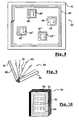
- FIGS. 9 and 10A device 50 according to the present invention, provided for such an application, is illustrated in FIGS. 9 and 10.
- the device 50looks like a notebook comprising a cover 51 and a back 52 made of cardboard or plastic, and “pages” 53 .
- the cover 51(or the back 52 ) incorporates a collective antenna 60 and each page receives or may receive one or more contactless electronic micromodules 61 of the type described above.
- each pageis a thin jacket made up of two plastic sheets, with one slot or several slots for the introduction of one or more micromodules 61 .
- Each micromodule 61takes the shape of a small plastic card incorporating a contactless integrated circuit and an individual antenna coil.
- each micromodule 61takes the shape of a silicon chip with integrated coil (“coil on chip”) fixed onto a plastic sheet arranged in a notebook with rings, spirals or binding.
- each micromodule 61is arranged according to an axis passing through the central part of the collective coil 51 , that is to say the part externally demarcated by the smallest turn in diameter of the collective coil.
- Each micromodule 61can therefore be read and/or written by means of a classical electronic label reader compatible with the anti-collision protocol implemented by the micromodules, by passing the reader in front of the cover 51 .
- FIG. 11represents a classical example of architecture of an integrated circuit 1 operating without contact 1 , connected to an individual antenna coil Ls which is itself coupled to a collective antenna coil Lc according to the present invention.
- the integrated circuit 1comprises an internal capacitor Cs forming with the individual antenna coil Ls a resonant antenna circuit of LC type, as well as a bridge rectifier Pd with diodes, a demodulation circuit DCT connected to the terminals of the antenna circuit LsCs, a load modulation circuit MCT, a central processing unit UC with hard-wired logic or microprocessor, and a memory array MEM.
- the memory array MEMcomprises a read-only memory (ROM), an electrically erasable and programmable read only memory (EEPROM) and a random access memory (RAM).
- the load modulation circuit MCTdrives a load modulation transistor T 1 which is connected to the terminals of the coil Ls through a load resistor R 1 .
- a magnetic field oscillating at 13.56 MHz for examplean induced alternating voltage Va amplified by the presence of the collective antenna Lc occurs at the terminals of the coil Ls.
- the voltage Vais rectified by the diode bridge Pd the output of which delivers a supply voltage Vcc of the integrated circuit.
- the data transmission from the reader RDT to the integrated circuit 1is carried out by modulating the amplitude of the magnetic field FLD sent by the reader.
- the induced voltage Vais demodulated by the circuit DCT that delivers the data received DTr to the central processing unit UC.
- the data transmission from the integrated circuit 1 to the reader RDTis carried out by modulating the load of the antenna coil Ls, which is passed onto the antenna coil Lp of the reader RDT.
- This load modulationis carried out by the modulator circuit MCT, which applies, to the transistor T 1 , a load modulation signal that depends on the data DTx to be transmitted, provided by the central processing unit UC.
- the central processing unit UCWhen the integrated circuit is activated by the field FLD after being in standby mode, the central processing unit UC begins by executing the steps of the anti-collision method chosen. The central processing unit UC waits for a general activation message to be received for example and determines upon receiving this message a random time for sending a response. If a message is received before the random time has elapsed, the central processing unit goes into standby mode while waiting for another general activation message.
Landscapes
- Engineering & Computer Science (AREA)
- Physics & Mathematics (AREA)
- Microelectronics & Electronic Packaging (AREA)
- Computer Hardware Design (AREA)
- General Physics & Mathematics (AREA)
- Theoretical Computer Science (AREA)
- Electromagnetism (AREA)
- Health & Medical Sciences (AREA)
- Computer Networks & Wireless Communication (AREA)
- Toxicology (AREA)
- General Health & Medical Sciences (AREA)
- Artificial Intelligence (AREA)
- Computer Vision & Pattern Recognition (AREA)
- Near-Field Transmission Systems (AREA)
- Credit Cards Or The Like (AREA)
- Telephone Function (AREA)
- Low-Molecular Organic Synthesis Reactions Using Catalysts (AREA)
- Lock And Its Accessories (AREA)
- Semiconductor Integrated Circuits (AREA)
Abstract
Description
Claims (9)
Applications Claiming Priority (3)
| Application Number | Priority Date | Filing Date | Title |
|---|---|---|---|
| FR0009997AFR2812482B1 (en) | 2000-07-28 | 2000-07-28 | PORTABLE ELECTRONIC DEVICE COMPRISING SEVERAL INTEGRATED NON-CONTACT CIRCUITS |
| FR0009997 | 2000-07-28 | ||
| PCT/FR2001/002149WO2002011061A1 (en) | 2000-07-28 | 2001-07-05 | Portable electronic device comprising several contact-free integrated circuits |
Related Parent Applications (1)
| Application Number | Title | Priority Date | Filing Date |
|---|---|---|---|
| PCT/FR2001/002149ContinuationWO2002011061A1 (en) | 2000-07-28 | 2001-07-05 | Portable electronic device comprising several contact-free integrated circuits |
Publications (1)
| Publication Number | Publication Date |
|---|---|
| US6774865B1true US6774865B1 (en) | 2004-08-10 |
Family
ID=8853079
Family Applications (1)
| Application Number | Title | Priority Date | Filing Date |
|---|---|---|---|
| US10/338,339Expired - LifetimeUS6774865B1 (en) | 2000-07-28 | 2003-01-08 | Portable electronic device comprising several contact-free integrated circuits |
Country Status (8)
| Country | Link |
|---|---|
| US (1) | US6774865B1 (en) |
| EP (1) | EP1305769B1 (en) |
| CN (1) | CN1180374C (en) |
| AT (1) | ATE406629T1 (en) |
| AU (1) | AU2001272628A1 (en) |
| DE (1) | DE60135556D1 (en) |
| FR (1) | FR2812482B1 (en) |
| WO (1) | WO2002011061A1 (en) |
Cited By (32)
| Publication number | Priority date | Publication date | Assignee | Title |
|---|---|---|---|---|
| US20040178274A1 (en)* | 2003-03-14 | 2004-09-16 | Chang-Ta Wu | Contactless radio frequency magnetic field data transmission card and its application system |
| US20050057409A1 (en)* | 2003-06-12 | 2005-03-17 | Hosung Choo | Electrically small planar antennas with inductively coupled feed |
| US20070095913A1 (en)* | 2003-06-06 | 2007-05-03 | Isao Takahashi | Antenna module and portable communication terminal equipped with the antenna module |
| US20070135456A1 (en)* | 2004-02-14 | 2007-06-14 | Pinto Ivan L | Medicaments with hm74a receptor activity |
| WO2007096789A1 (en) | 2006-02-24 | 2007-08-30 | Nxp B.V. | Transmitter, receiver, antenna arrangement for use with a transmitter or for use with a receiver, and rfid transponder |
| FR2899000A1 (en)* | 2006-03-24 | 2007-09-28 | Arjowiggins Security Soc Par A | Radiofrequency device e.g. inlay, for being integrated in e.g. passport, has wire type booster antenna formed with electrically insulated conductor wire and including turn that has two ends electrically connected in connection zone |
| WO2008031455A1 (en)* | 2006-09-11 | 2008-03-20 | Gemalto S.A. | Method and system for optimized reading of a radio frequency communication transponder with the aid of a passive resonant circuit |
| WO2008074050A1 (en) | 2006-12-18 | 2008-06-26 | Mikoh Corporation | A radio frequency identification tag with privacy and security capabilities |
| US20080164327A1 (en)* | 2005-07-07 | 2008-07-10 | Oberthur Card Systems Sa | Foldable Document With Non-Contact Electronic Device With Interference Means |
| US20080314989A1 (en)* | 2005-07-07 | 2008-12-25 | Oberthur Card Systems Sa | Document Having an Integrated Contactless Resonator Electronic Device |
| US20090040116A1 (en)* | 2005-05-25 | 2009-02-12 | Oberthur Card Systems Sa | Electronic entity with magnetic antenna |
| US20090224058A1 (en)* | 2008-03-05 | 2009-09-10 | Commissariat A L'energie Atomique | Contactless communication device |
| US20090289766A1 (en)* | 2006-06-30 | 2009-11-26 | Manfred Rietzler | Smartcard and method for the production of a smartcard |
| US20090315799A1 (en)* | 2005-05-25 | 2009-12-24 | Oberthur Card Systems Sa | Electronic Entity With Magnetic Antenna |
| US20100016681A1 (en)* | 2008-07-15 | 2010-01-21 | Charles Jr Harry K | Apparatus and Methods for Monitoring Physiological Functions |
| WO2011005550A3 (en)* | 2009-06-23 | 2011-04-07 | Avery Dennison Corporation | Washable rfid device for apparel tracking |
| US20110156864A1 (en)* | 2008-06-12 | 2011-06-30 | De La Rue International Limited | Security document, security systems and methods of controlling access to a region |
| US20110215909A1 (en)* | 2008-09-12 | 2011-09-08 | Arjowiggins Security | Structure including at least two integrated microcircuit devices with contactless communication |
| US20110270441A1 (en)* | 2004-09-13 | 2011-11-03 | Michael Handfield | Medicament container |
| EP2410470A1 (en)* | 2010-07-20 | 2012-01-25 | Oberthur Technologies | Microcircuit device including a means for amplifying the gain of an antenna |
| EP2179472A4 (en)* | 2007-08-02 | 2013-09-11 | Univ Pittsburgh | WIRELESS SYSTEMS COMPRISING MULTIPLE ELECTRONIC EQUIPMENT USING SIMPLIFIED MANUFACTURE AND ADAPTATION AND ASSOCIATED METHOD |
| US20150048928A1 (en)* | 2013-06-21 | 2015-02-19 | X-Card Holdings, Llc | Electronic credential signal activation systems and methods |
| US20150054704A1 (en)* | 2013-08-23 | 2015-02-26 | Samsung Sdi Co., Ltd. | Antenna module for terminal device and method for manufacturing the same |
| US9311591B2 (en) | 2012-07-02 | 2016-04-12 | Inside Secure | Antenna system for contactless microcircuit |
| GB2540690A (en)* | 2012-06-28 | 2017-01-25 | Murata Manufacturing Co | Antenna device, electricity supply element, and communication terminal device |
| US9726492B2 (en) | 2012-12-11 | 2017-08-08 | Murata Manufacturing Co., Ltd. | Angular velocity detection element |
| US9748634B2 (en) | 2012-06-28 | 2017-08-29 | Murata Manufacturing Co., Ltd. | Antenna device and communication terminal device |
| RU177093U1 (en)* | 2017-08-29 | 2018-02-07 | Эдуард Геннадьевич Новаковский | CONTACTLESS IDENTIFICATION SMART CARD WITH THE POSSIBILITY OF USING SEPARABLE FRAGMENTS AS AN ACTIVATED INDEPENDENT IDENTIFIERS WITH A UNIQUE CODE |
| WO2018044204A1 (en)* | 2016-09-02 | 2018-03-08 | Эдуард Геннадьевич НОВАКОВСКИЙ | Smart card in which detachable fragments can be used as independent rfid identifiers |
| RU2671303C1 (en)* | 2017-08-29 | 2018-10-30 | Эдуард Геннадьевич Новаковский | Non-contact identification smart-card with the possibility of using particular fragments as active self-identified identifiers with a unique code (variants) |
| WO2020016615A1 (en)* | 2018-07-20 | 2020-01-23 | Drayson Technologies (Europe) Limited | Circuitry for use in smart cards and other applications |
| WO2020188258A1 (en)* | 2019-03-15 | 2020-09-24 | Drayson Technologies (Europe) Limited | Electronics for use in smart cards and other near field rf communications enabled systems |
Families Citing this family (8)
| Publication number | Priority date | Publication date | Assignee | Title |
|---|---|---|---|---|
| FR2832241B1 (en) | 2001-11-09 | 2004-04-09 | Allibert Equipement | DEVICE TRACEABLE BY AN ELECTRONIC IDENTIFIER |
| FR2840431B1 (en) | 2002-05-29 | 2004-09-03 | Francois Trantoul | METHOD AND DEVICE FOR PROTECTING READING INSTRUCTIONS |
| US20080272885A1 (en)* | 2004-01-22 | 2008-11-06 | Mikoh Corporation | Modular Radio Frequency Identification Tagging Method |
| FR2887712B1 (en)* | 2005-06-24 | 2012-09-28 | Gemplus | METHOD AND SYSTEM FOR OPTIMIZED RADIO FREQUENCY COMMUNICATION TRANSPONDER READING USING A PASSIVE RESONANT CIRCUIT |
| FR2887665B1 (en) | 2005-06-27 | 2007-10-12 | Oberthur Card Syst Sa | ELECTRONIC ENTITY WITH MAGNETIC ANTENNA |
| EP1892651B1 (en)* | 2006-08-25 | 2008-08-13 | Winwatch SA | Analogue watch comprising a micro-transponder associated with an antenna-resonator intended for increasing the reading distance of said micro-transponder using an RFID reader |
| JP5125465B2 (en)* | 2007-12-11 | 2013-01-23 | ソニー株式会社 | Communication device |
| EP2279591A2 (en)* | 2008-04-18 | 2011-02-02 | Philips Intellectual Property & Standards GmbH | Method of commissioning a device arrangement |
Citations (14)
| Publication number | Priority date | Publication date | Assignee | Title |
|---|---|---|---|---|
| EP0101125A1 (en) | 1982-08-03 | 1984-02-22 | N.V. Nederlandsche Apparatenfabriek NEDAP | A coded responder for an electromagnetic detection system |
| US5461385A (en) | 1994-04-29 | 1995-10-24 | Hughes Identification Devices, Inc. | RF/ID transponder system employing multiple transponders and a sensor switch |
| US5574470A (en)* | 1994-09-30 | 1996-11-12 | Palomar Technologies Corporation | Radio frequency identification transponder apparatus and method |
| WO1997042578A1 (en) | 1996-05-06 | 1997-11-13 | Inside Technologies | Method for selecting an electronic module from a plurality of modules present in the query field of a terminal |
| WO1998002980A1 (en) | 1996-07-12 | 1998-01-22 | Inside Technologies | Device for transmitting and receiving digital data by electromagnetic induction and inductive coupling |
| WO1998002840A1 (en) | 1996-07-12 | 1998-01-22 | Inside Technologies S.A. | Demodulator of a signal received in a coil by electromagnetic induction |
| WO1998005123A1 (en) | 1996-07-31 | 1998-02-05 | Inside Technologies | Programmable switch, adjustable capacitance and resonant circuit effected by means of such a switch |
| WO1998006057A1 (en) | 1996-08-05 | 1998-02-12 | Inside Technologies | Microcircuit with contact and non-contact operating modes |
| WO1998006056A1 (en) | 1996-08-06 | 1998-02-12 | Inside Technologies | Non-contact integrated circuit comprising a charge pump |
| US5719586A (en) | 1992-05-15 | 1998-02-17 | Micron Communications, Inc. | Spherical antenna pattern(s) from antenna(s) arranged in a two-dimensional plane for use in RFID tags and labels |
| WO2000001013A1 (en) | 1998-06-29 | 2000-01-06 | Inside Technologies | Integrated electronic micromodule and method for making same |
| US6104278A (en)* | 1997-05-12 | 2000-08-15 | Meto International Gmbh | Universal anti-theft device and method for producing it |
| US6127989A (en)* | 1997-03-24 | 2000-10-03 | Em Microelectronic-Marin Sa | Monolithic integrated circuit and antenna coil structure comprising a peripheral protective ring |
| US6154137A (en)* | 1998-06-08 | 2000-11-28 | 3M Innovative Properties Company | Identification tag with enhanced security |
- 2000
- 2000-07-28FRFR0009997Apatent/FR2812482B1/ennot_activeExpired - Fee Related
- 2001
- 2001-07-05DEDE60135556Tpatent/DE60135556D1/ennot_activeExpired - Lifetime
- 2001-07-05WOPCT/FR2001/002149patent/WO2002011061A1/enactiveIP Right Grant
- 2001-07-05EPEP01951776Apatent/EP1305769B1/ennot_activeExpired - Lifetime
- 2001-07-05AUAU2001272628Apatent/AU2001272628A1/ennot_activeAbandoned
- 2001-07-05ATAT01951776Tpatent/ATE406629T1/ennot_activeIP Right Cessation
- 2001-07-05CNCNB01813551XApatent/CN1180374C/ennot_activeExpired - Lifetime
- 2003
- 2003-01-08USUS10/338,339patent/US6774865B1/ennot_activeExpired - Lifetime
Patent Citations (14)
| Publication number | Priority date | Publication date | Assignee | Title |
|---|---|---|---|---|
| EP0101125A1 (en) | 1982-08-03 | 1984-02-22 | N.V. Nederlandsche Apparatenfabriek NEDAP | A coded responder for an electromagnetic detection system |
| US5719586A (en) | 1992-05-15 | 1998-02-17 | Micron Communications, Inc. | Spherical antenna pattern(s) from antenna(s) arranged in a two-dimensional plane for use in RFID tags and labels |
| US5461385A (en) | 1994-04-29 | 1995-10-24 | Hughes Identification Devices, Inc. | RF/ID transponder system employing multiple transponders and a sensor switch |
| US5574470A (en)* | 1994-09-30 | 1996-11-12 | Palomar Technologies Corporation | Radio frequency identification transponder apparatus and method |
| WO1997042578A1 (en) | 1996-05-06 | 1997-11-13 | Inside Technologies | Method for selecting an electronic module from a plurality of modules present in the query field of a terminal |
| WO1998002840A1 (en) | 1996-07-12 | 1998-01-22 | Inside Technologies S.A. | Demodulator of a signal received in a coil by electromagnetic induction |
| WO1998002980A1 (en) | 1996-07-12 | 1998-01-22 | Inside Technologies | Device for transmitting and receiving digital data by electromagnetic induction and inductive coupling |
| WO1998005123A1 (en) | 1996-07-31 | 1998-02-05 | Inside Technologies | Programmable switch, adjustable capacitance and resonant circuit effected by means of such a switch |
| WO1998006057A1 (en) | 1996-08-05 | 1998-02-12 | Inside Technologies | Microcircuit with contact and non-contact operating modes |
| WO1998006056A1 (en) | 1996-08-06 | 1998-02-12 | Inside Technologies | Non-contact integrated circuit comprising a charge pump |
| US6127989A (en)* | 1997-03-24 | 2000-10-03 | Em Microelectronic-Marin Sa | Monolithic integrated circuit and antenna coil structure comprising a peripheral protective ring |
| US6104278A (en)* | 1997-05-12 | 2000-08-15 | Meto International Gmbh | Universal anti-theft device and method for producing it |
| US6154137A (en)* | 1998-06-08 | 2000-11-28 | 3M Innovative Properties Company | Identification tag with enhanced security |
| WO2000001013A1 (en) | 1998-06-29 | 2000-01-06 | Inside Technologies | Integrated electronic micromodule and method for making same |
Cited By (74)
| Publication number | Priority date | Publication date | Assignee | Title |
|---|---|---|---|---|
| US20040178274A1 (en)* | 2003-03-14 | 2004-09-16 | Chang-Ta Wu | Contactless radio frequency magnetic field data transmission card and its application system |
| US20070095913A1 (en)* | 2003-06-06 | 2007-05-03 | Isao Takahashi | Antenna module and portable communication terminal equipped with the antenna module |
| US7712672B2 (en)* | 2003-06-06 | 2010-05-11 | Sony Corporation | Antenna module and portable communication terminal equipped with the antenna module |
| US20050057409A1 (en)* | 2003-06-12 | 2005-03-17 | Hosung Choo | Electrically small planar antennas with inductively coupled feed |
| US7061440B2 (en)* | 2003-06-12 | 2006-06-13 | Board Of Regents, The University Of Texas System | Electrically small planar antennas with inductively coupled feed |
| US20070135456A1 (en)* | 2004-02-14 | 2007-06-14 | Pinto Ivan L | Medicaments with hm74a receptor activity |
| US20110270441A1 (en)* | 2004-09-13 | 2011-11-03 | Michael Handfield | Medicament container |
| US8712587B2 (en)* | 2004-09-13 | 2014-04-29 | Michael Handfield | Medicament container |
| US8378911B2 (en) | 2005-05-25 | 2013-02-19 | Oberthur Technologies | Electronic entity with magnetic antenna |
| US20090040116A1 (en)* | 2005-05-25 | 2009-02-12 | Oberthur Card Systems Sa | Electronic entity with magnetic antenna |
| US8698690B2 (en)* | 2005-05-25 | 2014-04-15 | Oberthur Technologies | Electronic entity with magnetic antenna |
| US20090315799A1 (en)* | 2005-05-25 | 2009-12-24 | Oberthur Card Systems Sa | Electronic Entity With Magnetic Antenna |
| US8157179B2 (en) | 2005-07-07 | 2012-04-17 | Oberthur Technologies | Document having an integrated contactless resonator electronic device |
| US20080164327A1 (en)* | 2005-07-07 | 2008-07-10 | Oberthur Card Systems Sa | Foldable Document With Non-Contact Electronic Device With Interference Means |
| US20080314989A1 (en)* | 2005-07-07 | 2008-12-25 | Oberthur Card Systems Sa | Document Having an Integrated Contactless Resonator Electronic Device |
| WO2007096789A1 (en) | 2006-02-24 | 2007-08-30 | Nxp B.V. | Transmitter, receiver, antenna arrangement for use with a transmitter or for use with a receiver, and rfid transponder |
| US20090242633A1 (en)* | 2006-02-24 | 2009-10-01 | Nxp B.V. | Transmitter, receiver, antenna arrangement for use with a transmitter or for use with a receive, and rfid transponder |
| US8746574B2 (en) | 2006-02-24 | 2014-06-10 | Nxp, B.V. | Transmitter, receiver, antenna arrangement for use with a transmitter or for use with a receive, and RFID transponder |
| WO2007118962A1 (en)* | 2006-03-24 | 2007-10-25 | Arjowiggins Security | Radiofrequency device |
| FR2899000A1 (en)* | 2006-03-24 | 2007-09-28 | Arjowiggins Security Soc Par A | Radiofrequency device e.g. inlay, for being integrated in e.g. passport, has wire type booster antenna formed with electrically insulated conductor wire and including turn that has two ends electrically connected in connection zone |
| US8040281B2 (en) | 2006-03-24 | 2011-10-18 | Arjowiggins Security | Radiofrequency device |
| US20090289766A1 (en)* | 2006-06-30 | 2009-11-26 | Manfred Rietzler | Smartcard and method for the production of a smartcard |
| US8427322B2 (en)* | 2006-06-30 | 2013-04-23 | Smartrac Ip B.V. | Smartcard and method for the production of a smartcard |
| CN101542499B (en)* | 2006-09-11 | 2013-04-24 | 格马尔托股份有限公司 | Method and system for optimized reading of a radio frequency communication transponder with the aid of a passive resonant circuit |
| US10146965B2 (en) | 2006-09-11 | 2018-12-04 | Gemalto Sa | Method and system for optimized reading of a radio frequency communication transponder with the aid of a passive resonant circuit |
| WO2008031455A1 (en)* | 2006-09-11 | 2008-03-20 | Gemalto S.A. | Method and system for optimized reading of a radio frequency communication transponder with the aid of a passive resonant circuit |
| US20090224888A1 (en)* | 2006-09-11 | 2009-09-10 | Gemalto Sa | Method and system for optimized reading of a radio frequency communication transponder with the aid of a passive resonant circuit |
| JP2010503084A (en)* | 2006-09-11 | 2010-01-28 | ジェマルト エスアー | Optimized reading method and system for transponders for high frequency communications using passive resonant circuits |
| US8381991B2 (en) | 2006-12-18 | 2013-02-26 | Mikoh Company | Radio frequency identification tag with privacy and security capabilities |
| US20100230498A1 (en)* | 2006-12-18 | 2010-09-16 | Peter Samuel Atherton | Radio frequency identification tag with privacy and security capabilities |
| EP2102799A4 (en)* | 2006-12-18 | 2010-03-31 | Mikoh Corp | A radio frequency identification tag with privacy and security capabilities |
| WO2008074050A1 (en) | 2006-12-18 | 2008-06-26 | Mikoh Corporation | A radio frequency identification tag with privacy and security capabilities |
| EP3002820A1 (en)* | 2007-08-02 | 2016-04-06 | University of Pittsburgh - Of the Commonwealth System of Higher Education | Wireless systems having multiple electronic devices and employing simplified fabrication and matching, and associated methods |
| US9131527B2 (en) | 2007-08-02 | 2015-09-08 | University of Pittsburgh—of the Commonwealth System of Higher Education | Wireless systems having multiple electronic devices and employing simplified fabrication and matching, and associated methods |
| EP2179472A4 (en)* | 2007-08-02 | 2013-09-11 | Univ Pittsburgh | WIRELESS SYSTEMS COMPRISING MULTIPLE ELECTRONIC EQUIPMENT USING SIMPLIFIED MANUFACTURE AND ADAPTATION AND ASSOCIATED METHOD |
| JP2009211696A (en)* | 2008-03-05 | 2009-09-17 | Commiss Energ Atom | Contactless communication device |
| US8141787B2 (en) | 2008-03-05 | 2012-03-27 | Commissariat A L'energie Atomique | Contactless communication device |
| US20090224058A1 (en)* | 2008-03-05 | 2009-09-10 | Commissariat A L'energie Atomique | Contactless communication device |
| US8988185B2 (en) | 2008-06-12 | 2015-03-24 | De La Rue International Limited | Security document, security systems and methods of controlling access to a region |
| US20110156864A1 (en)* | 2008-06-12 | 2011-06-30 | De La Rue International Limited | Security document, security systems and methods of controlling access to a region |
| US9486139B2 (en) | 2008-07-15 | 2016-11-08 | The Johns Hopkins University | Garment for monitoring physiological functions and method of use thereof |
| US8758241B2 (en)* | 2008-07-15 | 2014-06-24 | The Johns Hopkins University | Electronic module with keyed connection to a wearable garment for monitoring physiological functions and method of use |
| US20100016681A1 (en)* | 2008-07-15 | 2010-01-21 | Charles Jr Harry K | Apparatus and Methods for Monitoring Physiological Functions |
| US20110215909A1 (en)* | 2008-09-12 | 2011-09-08 | Arjowiggins Security | Structure including at least two integrated microcircuit devices with contactless communication |
| WO2011005550A3 (en)* | 2009-06-23 | 2011-04-07 | Avery Dennison Corporation | Washable rfid device for apparel tracking |
| CN102376010B (en)* | 2010-07-20 | 2016-12-28 | 欧贝特科技公司 | Microcircuit devices including the device for amplifying antenna gain |
| FR2963139A1 (en)* | 2010-07-20 | 2012-01-27 | Oberthur Technologies | MICROCIRCUIT DEVICE COMPRISING MEANS FOR AMPLIFYING THE GAIN OF AN ANTENNA |
| US8608082B2 (en) | 2010-07-20 | 2013-12-17 | Oberthur Technologies | Microcircuit device including means for amplifying the gain of an antenna |
| CN102376010A (en)* | 2010-07-20 | 2012-03-14 | 欧贝特科技公司 | Microcircuit equipment comprising device used for amplifying gain of antenne |
| EP2410470A1 (en)* | 2010-07-20 | 2012-01-25 | Oberthur Technologies | Microcircuit device including a means for amplifying the gain of an antenna |
| EP2998907A1 (en)* | 2010-07-20 | 2016-03-23 | Oberthur Technologies | Microcircuit device including means for amplifying the gain of an antenna |
| US9882267B2 (en) | 2012-06-28 | 2018-01-30 | Murata Manufacturing Co., Ltd. | Antenna device and communication terminal device |
| GB2519247B (en)* | 2012-06-28 | 2017-11-29 | Murata Manufacturing Co | Antenna device, feed element, and communication terminal device |
| GB2540690A (en)* | 2012-06-28 | 2017-01-25 | Murata Manufacturing Co | Antenna device, electricity supply element, and communication terminal device |
| US9748634B2 (en) | 2012-06-28 | 2017-08-29 | Murata Manufacturing Co., Ltd. | Antenna device and communication terminal device |
| GB2540690B (en)* | 2012-06-28 | 2017-09-27 | Murata Manufacturing Co | Antenna device, feed element, and communication terminal device |
| US9311591B2 (en) | 2012-07-02 | 2016-04-12 | Inside Secure | Antenna system for contactless microcircuit |
| US9726492B2 (en) | 2012-12-11 | 2017-08-08 | Murata Manufacturing Co., Ltd. | Angular velocity detection element |
| US10964146B2 (en) | 2013-06-21 | 2021-03-30 | X-Card Holdings, Llc | Electronic credential signal activation systems and methods |
| US12260695B2 (en) | 2013-06-21 | 2025-03-25 | X-Card Holdings, Llc | Electronic credential signal activation systems and methods |
| US9865105B2 (en)* | 2013-06-21 | 2018-01-09 | X-Card Holdings, Llc | Electronic credential signal activation systems and methods |
| US20150048928A1 (en)* | 2013-06-21 | 2015-02-19 | X-Card Holdings, Llc | Electronic credential signal activation systems and methods |
| US10255734B2 (en) | 2013-06-21 | 2019-04-09 | X-Card Holdings, Llc | Electronic credential signal activation systems and methods |
| US11734979B2 (en) | 2013-06-21 | 2023-08-22 | X-Card Holdings, Llc | Electronic credential signal activation systems and methods |
| US11417162B2 (en) | 2013-06-21 | 2022-08-16 | X-Card Holdings, Llc | Electronic credential signal activation systems and methods |
| US20150054704A1 (en)* | 2013-08-23 | 2015-02-26 | Samsung Sdi Co., Ltd. | Antenna module for terminal device and method for manufacturing the same |
| WO2018044204A1 (en)* | 2016-09-02 | 2018-03-08 | Эдуард Геннадьевич НОВАКОВСКИЙ | Smart card in which detachable fragments can be used as independent rfid identifiers |
| RU2671303C1 (en)* | 2017-08-29 | 2018-10-30 | Эдуард Геннадьевич Новаковский | Non-contact identification smart-card with the possibility of using particular fragments as active self-identified identifiers with a unique code (variants) |
| RU177093U1 (en)* | 2017-08-29 | 2018-02-07 | Эдуард Геннадьевич Новаковский | CONTACTLESS IDENTIFICATION SMART CARD WITH THE POSSIBILITY OF USING SEPARABLE FRAGMENTS AS AN ACTIVATED INDEPENDENT IDENTIFIERS WITH A UNIQUE CODE |
| CN112740231A (en)* | 2018-07-20 | 2021-04-30 | 德雷森技术(欧洲)有限公司 | Circuits for Smart Cards and Other Applications |
| WO2020016615A1 (en)* | 2018-07-20 | 2020-01-23 | Drayson Technologies (Europe) Limited | Circuitry for use in smart cards and other applications |
| US11995490B2 (en) | 2018-07-20 | 2024-05-28 | Freevolt Technologies Limited | Circuitry for use in smart cards and other applications |
| WO2020188258A1 (en)* | 2019-03-15 | 2020-09-24 | Drayson Technologies (Europe) Limited | Electronics for use in smart cards and other near field rf communications enabled systems |
| US11984917B2 (en) | 2019-03-15 | 2024-05-14 | Drayson Technologies (Europe) Limited | Electronics for use in smart cards and other near field RF communications enabled systems |
Also Published As
| Publication number | Publication date |
|---|---|
| CN1444754A (en) | 2003-09-24 |
| EP1305769B1 (en) | 2008-08-27 |
| ATE406629T1 (en) | 2008-09-15 |
| CN1180374C (en) | 2004-12-15 |
| FR2812482B1 (en) | 2003-01-24 |
| AU2001272628A1 (en) | 2002-02-13 |
| WO2002011061A1 (en) | 2002-02-07 |
| EP1305769A1 (en) | 2003-05-02 |
| DE60135556D1 (en) | 2008-10-09 |
| FR2812482A1 (en) | 2002-02-01 |
Similar Documents
| Publication | Publication Date | Title |
|---|---|---|
| US6774865B1 (en) | Portable electronic device comprising several contact-free integrated circuits | |
| US6809703B2 (en) | Contactless electronic tag for three-dimensional object | |
| US7119693B1 (en) | Integrated circuit with enhanced coupling | |
| US7893837B2 (en) | Packing material, tag, certificate, paper money, and securities | |
| US9767331B2 (en) | Methods and apparatus for preserving privacy in an RFID system | |
| JP5026522B2 (en) | Optimized reading method and system for transponders for high frequency communications using passive resonant circuits | |
| JP2007524942A (en) | Passive transmitter receiver device given by electromagnetic waves | |
| AU2003222275A1 (en) | Rectifier utilizing a grounded antenna | |
| US7453360B2 (en) | Identification-data media | |
| US20060055541A1 (en) | RFID tag having a silicon micro processing chip for radio frequency identification and a method of making the same | |
| US7046146B2 (en) | Electromagnetic field generation device for a transponder | |
| WO2002099764A1 (en) | Capacitively powered data communication system with tag and circuit carrier apparatus for use therein | |
| KR100682590B1 (en) | IOS card with heterogeneous RFID tags without frequency interference | |
| JP2001028037A (en) | Contactless information medium and communication system using the same | |
| Flor et al. | RFID: The integration of contactless identification technology and mobile computing | |
| KR101388156B1 (en) | Semiconductor device | |
| KR20080013215A (en) | RFID tag | |
| CN208722208U (en) | A kind of signal stiffening device | |
| JP2002056361A (en) | Non-contact type information recording medium reader and non-contact type information recording medium information processing system | |
| JP5427345B2 (en) | IC chip for RFID | |
| JP2001216485A (en) | Contactless information medium and communication system | |
| JP2008027168A (en) | Data carrier with multiple antennas |
Legal Events
| Date | Code | Title | Description |
|---|---|---|---|
| AS | Assignment | Owner name:INSIDE TECHNOLOGIES, FRANCE Free format text:ASSIGNMENT OF ASSIGNORS INTEREST;ASSIGNOR:SERRA, DIDIER;REEL/FRAME:013652/0611 Effective date:20020801 | |
| STCF | Information on status: patent grant | Free format text:PATENTED CASE | |
| FEPP | Fee payment procedure | Free format text:PAYOR NUMBER ASSIGNED (ORIGINAL EVENT CODE: ASPN); ENTITY STATUS OF PATENT OWNER: LARGE ENTITY | |
| FPAY | Fee payment | Year of fee payment:4 | |
| FPAY | Fee payment | Year of fee payment:8 | |
| FPAY | Fee payment | Year of fee payment:12 | |
| AS | Assignment | Owner name:INSIDE SECURE, FRANCE Free format text:CHANGE OF NAME;ASSIGNOR:INSIDE CONTACTLESS;REEL/FRAME:050297/0326 Effective date:20101231 Owner name:INSIDE CONTACTLESS, FRANCE Free format text:CHANGE OF NAME;ASSIGNOR:INSIDE TECHNOLOGIES;REEL/FRAME:050297/0282 Effective date:20030228 | |
| AS | Assignment | Owner name:VERIMATRIX, FRANCE Free format text:CHANGE OF NAME;ASSIGNOR:INSIDE SECURE;REEL/FRAME:050647/0428 Effective date:20190624 | |
| AS | Assignment | Owner name:VERIMATRIX, FRANCE Free format text:CHANGE OF ADDRESS;ASSIGNOR:VERIMATRIX;REEL/FRAME:050733/0003 Effective date:20190930 |