US6774437B2 - Fin-based double poly dynamic threshold CMOS FET with spacer gate and method of fabrication - Google Patents
Fin-based double poly dynamic threshold CMOS FET with spacer gate and method of fabricationDownload PDFInfo
- Publication number
- US6774437B2 US6774437B2US09/683,486US68348602AUS6774437B2US 6774437 B2US6774437 B2US 6774437B2US 68348602 AUS68348602 AUS 68348602AUS 6774437 B2US6774437 B2US 6774437B2
- Authority
- US
- United States
- Prior art keywords
- transistor
- gate structure
- gate
- edge
- transistor body
- Prior art date
- Legal status (The legal status is an assumption and is not a legal conclusion. Google has not performed a legal analysis and makes no representation as to the accuracy of the status listed.)
- Expired - Lifetime
Links
Images


Classifications
- H—ELECTRICITY
- H10—SEMICONDUCTOR DEVICES; ELECTRIC SOLID-STATE DEVICES NOT OTHERWISE PROVIDED FOR
- H10D—INORGANIC ELECTRIC SEMICONDUCTOR DEVICES
- H10D30/00—Field-effect transistors [FET]
- H10D30/60—Insulated-gate field-effect transistors [IGFET]
- H10D30/62—Fin field-effect transistors [FinFET]
- H—ELECTRICITY
- H01—ELECTRIC ELEMENTS
- H01L—SEMICONDUCTOR DEVICES NOT COVERED BY CLASS H10
- H01L21/00—Processes or apparatus adapted for the manufacture or treatment of semiconductor or solid state devices or of parts thereof
- H01L21/02—Manufacture or treatment of semiconductor devices or of parts thereof
- H01L21/04—Manufacture or treatment of semiconductor devices or of parts thereof the devices having potential barriers, e.g. a PN junction, depletion layer or carrier concentration layer
- H01L21/18—Manufacture or treatment of semiconductor devices or of parts thereof the devices having potential barriers, e.g. a PN junction, depletion layer or carrier concentration layer the devices having semiconductor bodies comprising elements of Group IV of the Periodic Table or AIIIBV compounds with or without impurities, e.g. doping materials
- H01L21/28—Manufacture of electrodes on semiconductor bodies using processes or apparatus not provided for in groups H01L21/20 - H01L21/268
- H01L21/28008—Making conductor-insulator-semiconductor electrodes
- H01L21/28017—Making conductor-insulator-semiconductor electrodes the insulator being formed after the semiconductor body, the semiconductor being silicon
- H01L21/28026—Making conductor-insulator-semiconductor electrodes the insulator being formed after the semiconductor body, the semiconductor being silicon characterised by the conductor
- H01L21/28123—Lithography-related aspects, e.g. sub-lithography lengths; Isolation-related aspects, e.g. to solve problems arising at the crossing with the side of the device isolation; Planarisation aspects
- H01L21/2815—Lithography-related aspects, e.g. sub-lithography lengths; Isolation-related aspects, e.g. to solve problems arising at the crossing with the side of the device isolation; Planarisation aspects part or whole of the electrode is a sidewall spacer or made by a similar technique, e.g. transformation under mask, plating
- H—ELECTRICITY
- H10—SEMICONDUCTOR DEVICES; ELECTRIC SOLID-STATE DEVICES NOT OTHERWISE PROVIDED FOR
- H10D—INORGANIC ELECTRIC SEMICONDUCTOR DEVICES
- H10D30/00—Field-effect transistors [FET]
- H10D30/01—Manufacture or treatment
- H10D30/021—Manufacture or treatment of FETs having insulated gates [IGFET]
- H10D30/024—Manufacture or treatment of FETs having insulated gates [IGFET] of fin field-effect transistors [FinFET]
- H—ELECTRICITY
- H10—SEMICONDUCTOR DEVICES; ELECTRIC SOLID-STATE DEVICES NOT OTHERWISE PROVIDED FOR
- H10D—INORGANIC ELECTRIC SEMICONDUCTOR DEVICES
- H10D30/00—Field-effect transistors [FET]
- H10D30/60—Insulated-gate field-effect transistors [IGFET]
- H10D30/67—Thin-film transistors [TFT]
- H10D30/6729—Thin-film transistors [TFT] characterised by the electrodes
- H10D30/673—Thin-film transistors [TFT] characterised by the electrodes characterised by the shapes, relative sizes or dispositions of the gate electrodes
- H—ELECTRICITY
- H10—SEMICONDUCTOR DEVICES; ELECTRIC SOLID-STATE DEVICES NOT OTHERWISE PROVIDED FOR
- H10D—INORGANIC ELECTRIC SEMICONDUCTOR DEVICES
- H10D30/00—Field-effect transistors [FET]
- H10D30/60—Insulated-gate field-effect transistors [IGFET]
- H10D30/721—Insulated-gate field-effect transistors [IGFET] having a gate-to-body connection, i.e. bulk dynamic threshold voltage IGFET
- H—ELECTRICITY
- H10—SEMICONDUCTOR DEVICES; ELECTRIC SOLID-STATE DEVICES NOT OTHERWISE PROVIDED FOR
- H10D—INORGANIC ELECTRIC SEMICONDUCTOR DEVICES
- H10D86/00—Integrated devices formed in or on insulating or conducting substrates, e.g. formed in silicon-on-insulator [SOI] substrates or on stainless steel or glass substrates
- H10D86/01—Manufacture or treatment
- H—ELECTRICITY
- H10—SEMICONDUCTOR DEVICES; ELECTRIC SOLID-STATE DEVICES NOT OTHERWISE PROVIDED FOR
- H10D—INORGANIC ELECTRIC SEMICONDUCTOR DEVICES
- H10D86/00—Integrated devices formed in or on insulating or conducting substrates, e.g. formed in silicon-on-insulator [SOI] substrates or on stainless steel or glass substrates
- H10D86/201—Integrated devices formed in or on insulating or conducting substrates, e.g. formed in silicon-on-insulator [SOI] substrates or on stainless steel or glass substrates the substrates comprising an insulating layer on a semiconductor body, e.g. SOI
Definitions
- the present inventionrelates generally to the field of semiconductor manufacturing and, more specifically, to a dynamic threshold (DT) complementary metal oxide semiconductor (CMOS) field effect transistor (FET) device and method for forming same.
- DTdynamic threshold
- CMOScomplementary metal oxide semiconductor
- FETfield effect transistor
- CMOScomplementary metal-oxide-semiconductor
- FETsare used in almost all types of integrated circuit design (i.e., microprocessors, memory, etc.).
- CMOS FETscan result in degradation of performance and/or reliability.
- CMOS field effect transistorOne type of FET that has been proposed to facilitate increased device density is a dynamic threshold CMOS field effect transistor. Dynamic thresholding is achieved by electrically connecting the gate to the body, so that the body voltage moves with the gate voltage, lowering the threshold voltage when a signal is present. Dynamic thresholding provides faster response time and lower power consumption for the FET. Threshold voltage (Vt) is high in the off-state, limiting power leakage, and low in the on-state, limiting power requirements. CMOS generally uses less power than ordinary MOS. Dynamic threshold CMOS uses less power than standard CMOS.
- the inventioncomprises a method for forming a transistor, the method comprising the steps of a) providing a semiconductor substrate; b) patterning the semiconductor substrate to provide a first body edge; c) providing a gate structure adjacent the first body edge; d) patterning the semiconductor substrate to provide a second body edge, the first and second body edges of the semiconductor substrate defining a transistor body; e) providing a body contact structure adjacent the second body edge aligned to the gate structure; and f) providing an electrically connective bridge between the gate structure and the body contact structure over the transistor body.
- the inventioncomprises A transistor comprising: a) a transistor body formed on a substrate, the transistor body having a first vertical edge and a second vertical edge; b) a gate structure adjacent the transistor body first vertical edge; c) a body contact structure adjacent the transistor body second vertical edge and aligned with the gate; d) a bridge over the body, the gate, and the body contact, electrically connecting the gate and the body contact; and e) source and drain regions in the body on opposite ends of the body.
- the present inventionprovides a fin-based dynamic threshold (DT) complimentary metal oxide semiconductor (CMOS) field effect transistor (FET) and methods for forming same that results in improved device performance and density.
- DTdynamic threshold
- CMOScomplimentary metal oxide semiconductor
- FETfield effect transistor
- FIG. 1is a process flow chart showing the exemplary steps of fabrication of a DT CMOS FET
- the present inventionprovides a dynamic threshold (DT) complimentary metal oxide semiconductor (CMOS) field-effect transistor (FET) and a method for forming the same that results in improved device performance and density.
- CMOScomplimentary metal oxide semiconductor
- the preferred embodiment of the present inventionprovides a DT CMOS FET on a semiconductor body with a gate on a first long side, a body contact an the opposite long side, and a bridge over the body electrically connecting the gate and the body contact.
- the gate and body contactare located between the source and drain portions of the FET.
- the source and drainare formed by ion implantation doping when the body is exposed.
- Fin-based DT CMOS FETsfeature a long, thin semiconductor body vertically disposed on a substrate. Vertical orientation of the fin reduces the planar area occupied by the DT CMOS FET on the chip.
- the insulated gateis formed on one long side of the body, and the body contact is located on the opposite long side of the body, with the transistor body being disposed horizontally between the gate and the body contact.
- the gate and the body contactare electrically connected by a bridge over the body. Because the body is thin between the gate and the body contact, the bridge provides a short, low resistance path.
- the thin fin bodyalso reduces body-to-source/drain capacitance.
- the ends of the fin, outside of the region of the gate and body contact,are appropriately doped to provide source and drain regions.
- the preferred method for forming these DT CMOS FETsallows the gate length of the device to have minimum feature size, while allowing the thickness of the body to be much smaller than the gate length (preferably less than one-third of the gate length).
- the preferred method for forming the DT CMOS FETis accomplished by using an image enhancement technique, sidewall image transfer, to define the thickness of the transistor body, allowing it to be reliably formed at sub minimum feature size.
- FIG. 1the steps of the method for forming an exemplary DT CMOS FET in accordance with the preferred embodiment are illustrated.
- the methodforms a DT CMOS FET in a way that improves the response time of the transistor, while maintaining fabrication reliability and simplicity.
- the first step 101is to provide, as illustrated by example in FIG. 2, an appropriate wafer 200 , 204 , and 202 , deposit etch stop layers 206 and 208 , and deposit a mandrel layer 212 .
- the wafer usedcomprises a silicon 202 on insulator 204 (SOI) wafer.
- SOIsilicon 202 on insulator 204
- the wafercomprises a substrate 200 beneath a bottom oxide layer 204 beneath a single crystal silicon layer 202 .
- the bottom oxide 204 and single crystal silicon layer 202together form the SOI layer.
- the single crystal silicon layer 202is used to form the fin body of the DT CMOS FET.
- an etch stop layeris deposited, comprising an oxide layer 206 on the silicon layer 202 and silicon nitride 208 on top of that oxide layer 206 .
- the etch stop layerwill be used for etch stopping and creating an insulator on the top of the fin in the final product.
- a mandrel layer 212is then formed on the nitride 208 , preferably comprising silicon dioxide. This mandrel layer 212 will be used in the fabrication process as a block mask for defining a first edge to the fin and for supporting a sidewall spacer used in sidewall image transfer.
- step 102referring to the example in FIG. 3, an unmasked portion of the silicon dioxide mandrel layer 212 is vertically etched to the etch stop layer 208 . Maintaining the etch stop layer is important because etch stop layer 206 will later become the insulator between the bridge and the body of the transistor.
- the thickness of the silicon dioxide layer 212should be greater than the desired width of the spacer 301 to be formed in the next step, in order to make the width of spacer 301 insensitive to the thickness of layer 212 .
- a silicon nitride sidewall spacer 301is formed on the side of the silicon dioxide layer 212 using the method well known in the art of conformally coating the sidewall area with silicon nitride (not shown) and then vertically etching to leave a sidewall spacer 301 in place.
- the anisotropic etching which forms the silicon nitride sidewall spacer 301also etches through the silicon nitride etch stop layer 208 .
- a subsequent masked anisotropic etching of the silicon dioxide 206 selective to silicon nitride 208 , 301 and siliconreaches the single crystal silicon layer 202 .
- the sidewall spacer 301rests upon a portion of the etch stop layer 208 .
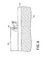
- step 104the silicon layer 202 is etched, selective to silicon nitride, to reach the bottom oxide layer 204 and expose a first edge of silicon 202 which will become a long side of the fin structure.
- a gate oxide 401is formed on the silicon 202 sidewall by forming a first, sacrificial oxide, wet-stripping it, and then forming the gate oxide 401 .
- the gate oxide 401will ultimately become the insulator for the gate.
- an n+ polysilicon sidewall spacer 501is formed over the gate oxide 401 , the etch stop layers 206 and 208 and silicon nitride spacer 301 upon the bottom oxide layer 204 .
- the top of the n+ polysilicon spacer 501is formed below the level of the top of the silicon dioxide layer 212 .
- the n+ polysilicon spacer 501will eventually become the gate.
- step 107a silicon nitride conformal coating 601 is formed over the bottom oxide 204 , the mandrel layer 212 , and the structures in between 301 501 .
- This layer 601must have a thickness greater than the top of the mandrel layer 212 relative to the top of the bottom oxide 202 .
- the conformal silicon nitride 601is planarized, as shown in the example of FIG. 7, to below the top of the silicon dioxide mandrel layer 212 by chemical mechanical planarization (CMP) and reactive ion etch (RIE).
- CMPchemical mechanical planarization
- RIEreactive ion etch
- the portion of the silicon dioxide mandrel layer 212 exposed by planarizationis vertically etched selective to silicon nitride 301 , 601 to the etch stop layer.
- the top etch stop layer 208is vertically (anisotopically) etched selective to silicon dioxide 206 .
- the silicon dioxide etch stop layer 206is anisotropically etched selective to silicon 202 .
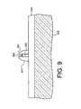
- the silicon layer 202 , exclusive of the portion below the silicon nitride spacer 301 and the remnants of the etch stop layer 206 , 208is anisotropically etched selectively with respect to silicon nitride 301 , 601 . This process exposes a second edge of the transistor fin body 202 , being a second long sidewall of the fin structure.
- the single crystal silicon layer remnant 202is the fin 202 .
- a native oxide 701is formed by atomic layer oxidation on the silicon 202 sidewall as a diffusion barrier 701 . This formation can be by exposure to air or the oxidation can be compelled.
- the oxide layer 701serves as a barrier to the diffusion of Boron from the yet-to-be-formed p+ polysilicon body contact 801 into the single crystal silicon 202 during subsequent annealing steps.
- a p+ polysilicon sidewall spacer 801is formed against the second sidewall's native oxide layer 701 , the etch stop layers 206 208 , the silicon nitride sidewall spacer 30 , and upon the bottom oxide layer 204 .
- This sidewall spacerwill become the body contact electrode 801 .
- the p+ polysilicon 801can be doped before or after deposition.
- the remaining silicon nitride 601 , 301 , 208is etched selectively with respect to polysilicon 501 , 801 and silicon dioxide 204 , 206 .
- the silicon nitride of the original sidewall spacer 301 and the silicon nitride of the etch stop layer 208are etched away in this step.
- the silicon dioxide layer 206 of the etch stop layerremains on the top of the fin 202 to form an insulator 206 between the fin 202 and yet-to-be-formed bridge 1501 .
- an intrinsic polysilicon 1001is deposited and planarized to a level higher than the n+ and p+ polysilicon sidewall spacers 501 , 801 .
- the purpose of layer 1001is to provide a flat surface for a photolithography mask.
- a photo resist 1101is added and patterned via photo lithography. Negative or positive photo resist may be used. This is preferably done using standard lithographic techniques, i.e, depositing and patterning a hardmask, and then using the patterned hardmask as an etch block during an etching of the exposed materials.
- the exposed portions of the photo resist 1101are etched as shown in the example of FIG. 12 .
- the polysilicon spacers 501 , 801are etched to define the gate 501 length and body contact 801 length and to expose the fin body 202 .
- the gate 501 lengthshould be greater than three times the thickness of the fin 202 .
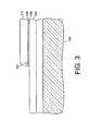
- FIG. 12 ashows a plan view of the device after etching the pattern through a photo resist 1101 mask. In the augmented plan view, the gate 501 , gate insulator 401 , body contact 801 , intrinsic silicon 1001 and the portion of the fin 202 between the gate 501 and the body contact 801 are shown in addition to the standard view.
- FIG. 12 billustrates a vertical sectional view (A-A′), transverse to the fin's 202 long axis and through the polysilicon spacers 501 , 801 , after etching away the exposed intrinsic polysilicon 1001 to provide side isolation regions.
- FIG. 12 cis an augmented vertical sectional view (B-B′) through the fin's 202 long axis also showing the polysilicon gate 501 and the unexposed photo resist 1101 .
- This viewshows the result of etching the intrinsic silicon 1001 , n+ polysilicon 501 , and p+ polysilicon 801 through a resist mask to define the side boundaries of the gate 501 and body contact 801 and to expose the fin body 202 outside of the side boundaries of gate 501 and body contact 801 .
- the etchingis anisotropic and selective against silicon dioxide to protect the fin 202 top insulator 206 and the bottom oxide 204 .
- FIG. 13 ais an augmented plan view of the device showing the directions 1301 for ion implantation.
- Gate 501is shown as a hatched region in all three views. Two sectional views are defined.
- FIG. 13 billustrates a vertical sectional view (A-A′) transverse to the fin's 202 long axis and through the polysilicon spacers 501 , 801 and remaining intrinsic polysilicon 1001 .
- 13 cis an augmented vertical sectional view (B-B′) through the fin 202 and along its long axis showing the remaining intrinsic silicon 1001 and additionally showing the gate 501 which is behind the sectional plane.
- the exposed ends of the silicon fin 202are doped using an ion implant technique from four angles, forty-five degrees from the fin axis. This produces uniformity of doping density.
- Arsenic ionsare implanted for nFETs and Boron ions are implanted for pFETs.
- ion implantationcan take place at any point in the process when a sidewall of the fin 202 is exposed, such as before the gate oxide 401 is formed and before the diffusion barrier native oxide 701 is formed.
- step 122as illustrated in the example of FIG. 14, sidewall spacers 1402 are added to the exposed portions of the fin 202 .
- Sidewall spacers 1401are added to the sides of the gate 501 and body contact 801 , and to the intrinsic polysilicon mesa 1001 which encloses the remaining portions of the gate 501 and the body contact 801 .
- FIG. 14 ais an augmented plan view of the device showing the addition of silicon nitride sidewall spacers 1401 to the sides of the polysilicon electrodes and the sidewalls of the intrinsic polysilicon mesa.
- the sidewall spacers 1401are shown cross hatched differently from the gate in all three views.
- Silicon nitride sidewall spacers 1402cover the sides and ends of the fin. Because fin spacers 1402 and gate-side spacers 1401 are of different heights, there are multiple sub-steps within step 122 to accomplish the result. Two sectional views of FIG. 14 a are defined.
- FIG. 14 bis an augmented vertical section (A-A′) through the polysilicon gate 501 and body contact 801 and transverse to the long axis of the fin 202 . Additionally, FIG. 14 b shows the sidewall spacers 1402 which are out of the sectional plane.
- the silicon nitride spacers 1401 , 1402are formed by conformal deposition and anisotropic etching.
- FIG. 14 cis an augmented vertical sectional view (B-B′) along the long axis of the fin 202 showing the remaining intrinsic silicon 1001 and the fin's 202 end spacers 1402 . Additionally, FIG. 14 c shows the gate 501 and its side spacers 1401 which are not in the sectional plane.
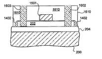
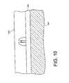
- FIG. 15 ais a plan view of the device showing a metal silicide bridge 1501 on the intrinsic silicon 1001 , the sidewall spacers 1401 and 1402 , and the insulator 206 on top of the fin 202 .
- the bridgeis formed by deposition of cobalt and subsequent annealing to form cobalt silicide.
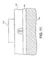
- FIG. 15 bis a sectional view (A-A′) showing the cobalt silicide bridge 1501 being insulated from the fin 202 by the oxide layer remnant 206 (not labeled) and further showing the connection between the gate 501 and the body contact 801 by the bridge 1501 .
- FIG. 15 cis a vertical sectional view (B-B′) along the long axis of the fin 202 showing the bridge 1501 insulated from the fin 202 by the oxide layer 206 .
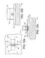
- FIG. 16 ais a plan view of the device after contacts 1601 - 1603 have been formed.
- FIG. 16 bis a vertical section view (A-A′) transverse to the long axis of the fin 202 and through the polysilicon structures 501 and 801 showing the contact 1601 for the gate 501 .
- the contactis formed by deposition and planarization of an insulator (silicon dioxide) 1610 on the device, etching of contact holes in the silicon dioxide into the cobalt silicide layer, and filling the etched holes with tungsten.
- FIG. 1is a plan view of the device after contacts 1601 - 1603 have been formed.
- FIG. 16 bis a vertical section view (A-A′) transverse to the long axis of the fin 202 and through the polysilicon structures 501 and 801 showing the contact 1601 for the gate 501 .
- the contactis formed by deposition and planarization of an insulator (silicon dioxide) 1610 on the device, etch
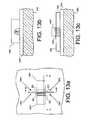
- 16 cshows a vertical sectional view (B-B′) along the long axis of the fin 202 with source and drain contacts 1602 - 1603 but without showing the gate contact 1601 , which is out of the sectional plane.
- the source and drain contacts 1602 - 1603are formed by means similar to the means used to form the gate contact but there is no cobalt silicide on the source and drain regions of the fin 202 .
- the etching of the contact holesremoves the portions of the fin's 202 silicon nitride sidewall spacers 1402 that cover the source and drain regions.
- the contacts 1602 - 1603connect directly with the doped silicon source and drain regions of the fin 202 .
- the source and drain contacts 1602 - 1603may be formed at the same time as the gate contact 1601 or as an additional step.
- metalizationfollows to form interconnects to other transistors (not shown).
- the preferred embodiment of the present inventionwas implemented using a fin type structure 202 .
- the fin-based DT CMOS FETfeatured a long, thin semiconductor body 202 vertically disposed on a substrate, also known as a fin 202 . Vertical orientation of the fin reduced the planar area occupied by the DT CMOS FET on the chip.
- the gate 501was formed on one long side of the body 202
- the body contact 801was formed on the opposite long side of the body 202 , with the fin 202 disposed horizontally between the gate 501 and the body contact 801 .
- the gate 501 and the body contact 801were electrically connected by a bridge 1501 over the body 202 .
- the bridge 1501provided a short, low resistance path.
- the thin fin 202 bodyalso reduced body-to-source/drain capacitance.
- the ends of the fin 202outside of the region of the gate 501 and body contact 801 , were appropriately doped to provide source and drain regions.
- the preferred method for forming these DT CMOS FETsallowed the gate 501 length of the device to have minimum feature size, while allowing the thickness of the fin 202 to be much less than the gate 501 length, preferably less than one-third of the gate length.
- the preferred method for forming the DT CMOS FETwas accomplished by using an image enhancement technique, sidewall image transfer, to define the thickness of the transistor body 202 , allowing it to be reliably formed at sub minimum feature size.
Landscapes
- Engineering & Computer Science (AREA)
- Physics & Mathematics (AREA)
- Condensed Matter Physics & Semiconductors (AREA)
- General Physics & Mathematics (AREA)
- Manufacturing & Machinery (AREA)
- Computer Hardware Design (AREA)
- Microelectronics & Electronic Packaging (AREA)
- Power Engineering (AREA)
- Metal-Oxide And Bipolar Metal-Oxide Semiconductor Integrated Circuits (AREA)
- Insulated Gate Type Field-Effect Transistor (AREA)
- Thin Film Transistor (AREA)
Abstract
Description
Claims (18)
Priority Applications (2)
| Application Number | Priority Date | Filing Date | Title |
|---|---|---|---|
| US09/683,486US6774437B2 (en) | 2002-01-07 | 2002-01-07 | Fin-based double poly dynamic threshold CMOS FET with spacer gate and method of fabrication |
| US10/843,029US6913960B2 (en) | 2002-01-07 | 2004-05-11 | Fin-based double poly dynamic threshold CMOS FET with spacer gate and method of fabrication |
Applications Claiming Priority (1)
| Application Number | Priority Date | Filing Date | Title |
|---|---|---|---|
| US09/683,486US6774437B2 (en) | 2002-01-07 | 2002-01-07 | Fin-based double poly dynamic threshold CMOS FET with spacer gate and method of fabrication |
Related Child Applications (1)
| Application Number | Title | Priority Date | Filing Date |
|---|---|---|---|
| US10/843,029DivisionUS6913960B2 (en) | 2002-01-07 | 2004-05-11 | Fin-based double poly dynamic threshold CMOS FET with spacer gate and method of fabrication |
Publications (2)
| Publication Number | Publication Date |
|---|---|
| US20030127690A1 US20030127690A1 (en) | 2003-07-10 |
| US6774437B2true US6774437B2 (en) | 2004-08-10 |
Family
ID=24744253
Family Applications (2)
| Application Number | Title | Priority Date | Filing Date |
|---|---|---|---|
| US09/683,486Expired - LifetimeUS6774437B2 (en) | 2002-01-07 | 2002-01-07 | Fin-based double poly dynamic threshold CMOS FET with spacer gate and method of fabrication |
| US10/843,029Expired - Fee RelatedUS6913960B2 (en) | 2002-01-07 | 2004-05-11 | Fin-based double poly dynamic threshold CMOS FET with spacer gate and method of fabrication |
Family Applications After (1)
| Application Number | Title | Priority Date | Filing Date |
|---|---|---|---|
| US10/843,029Expired - Fee RelatedUS6913960B2 (en) | 2002-01-07 | 2004-05-11 | Fin-based double poly dynamic threshold CMOS FET with spacer gate and method of fabrication |
Country Status (1)
| Country | Link |
|---|---|
| US (2) | US6774437B2 (en) |
Cited By (12)
| Publication number | Priority date | Publication date | Assignee | Title |
|---|---|---|---|---|
| US20040127004A1 (en)* | 1999-02-02 | 2004-07-01 | Toshihiro Honma | Manufacturing method which prevents abnormal gate oxidation |
| US20060231873A1 (en)* | 2005-04-14 | 2006-10-19 | International Business Machines Corporation | PLANAR DUAL-GATE FIELD EFFECT TRANSISTORS (FETs) |
| US20070023756A1 (en)* | 2005-07-27 | 2007-02-01 | International Business Machines Corporation | Virtual body-contacted trigate |
| US20080161754A1 (en)* | 2006-12-29 | 2008-07-03 | Medsolve Technologies, Inc. | Method and apparatus for infusing liquid to a body |
| US20080224213A1 (en)* | 2007-03-14 | 2008-09-18 | International Business Machines Corporation | Process for making finfet device with body contact and buried oxide junction isolation |
| US7476578B1 (en) | 2007-07-12 | 2009-01-13 | International Business Machines Corporation | Process for finFET spacer formation |
| US20090302402A1 (en)* | 2008-06-04 | 2009-12-10 | Anderson Brent A | Mugfet with stub source and drain regions |
| US20100155842A1 (en)* | 2008-12-23 | 2010-06-24 | International Business Machines Corporation | Body contacted hybrid surface semiconductor-on-insulator devices |
| US20110111596A1 (en)* | 2009-11-06 | 2011-05-12 | International Business Machine Corporation | Sidewall Image Transfer Using the Lithographic Stack as the Mandrel |
| US20120007180A1 (en)* | 2010-07-06 | 2012-01-12 | Globalfoundries Singapore PTE, LTD. | FinFET with novel body contact for multiple Vt applications |
| US8202267B2 (en) | 2006-10-10 | 2012-06-19 | Medsolve Technologies, Inc. | Method and apparatus for infusing liquid to a body |
| US8708961B2 (en) | 2008-01-28 | 2014-04-29 | Medsolve Technologies, Inc. | Apparatus for infusing liquid to a body |
Families Citing this family (18)
| Publication number | Priority date | Publication date | Assignee | Title |
|---|---|---|---|---|
| KR100474850B1 (en)* | 2002-11-15 | 2005-03-11 | 삼성전자주식회사 | Silicon/Oxide/Nitride/Oxide/Silicon nonvolatile memory with vertical channel and Fabricating method thereof |
| US7105894B2 (en)* | 2003-02-27 | 2006-09-12 | Taiwan Semiconductor Manufacturing Co., Ltd. | Contacts to semiconductor fin devices |
| US7074656B2 (en)* | 2003-04-29 | 2006-07-11 | Taiwan Semiconductor Manufacturing Company, Ltd. | Doping of semiconductor fin devices |
| US7183780B2 (en)* | 2004-09-17 | 2007-02-27 | International Business Machines Corporation | Electrical open/short contact alignment structure for active region vs. gate region |
| US20060084243A1 (en)* | 2004-10-20 | 2006-04-20 | Ying Zhang | Oxidation sidewall image transfer patterning method |
| EP1892765A1 (en)* | 2006-08-23 | 2008-02-27 | INTERUNIVERSITAIR MICROELEKTRONICA CENTRUM vzw (IMEC) | Method for doping a fin-based semiconductor device |
| EP1916717A3 (en)* | 2006-08-23 | 2010-12-22 | Imec | Method for doping a fin-based semiconductor device |
| US7550773B2 (en)* | 2007-06-27 | 2009-06-23 | International Business Machines Corporation | FinFET with top body contact |
| US7485520B2 (en)* | 2007-07-05 | 2009-02-03 | International Business Machines Corporation | Method of manufacturing a body-contacted finfet |
| US7910994B2 (en)* | 2007-10-15 | 2011-03-22 | Taiwan Semiconductor Manufacturing Company, Ltd. | System and method for source/drain contact processing |
| US7937675B2 (en)* | 2007-11-06 | 2011-05-03 | International Business Machines Corporation | Structure including transistor having gate and body in direct self-aligned contact |
| US8993402B2 (en) | 2012-08-16 | 2015-03-31 | International Business Machines Corporation | Method of manufacturing a body-contacted SOI FINFET |
| CN103681335B (en)* | 2012-09-17 | 2017-07-11 | 中国科学院微电子研究所 | Semiconductor device manufacturing method |
| KR101994079B1 (en) | 2012-10-10 | 2019-09-30 | 삼성전자 주식회사 | Semiconductor device and fabricated method thereof |
| CN103855026B (en) | 2012-12-06 | 2017-04-19 | 中国科学院微电子研究所 | Finfet and manufacturing method thereof |
| CN103855027B (en) | 2012-12-06 | 2017-01-25 | 中国科学院微电子研究所 | Finfet and manufacturing method thereof |
| US9142674B2 (en)* | 2013-03-15 | 2015-09-22 | GlobalFoundries, Inc. | FINFET devices having a body contact and methods of forming the same |
| US10930565B2 (en) | 2018-11-01 | 2021-02-23 | International Business Machines Corporation | III-V CMOS co-integration |
Citations (12)
| Publication number | Priority date | Publication date | Assignee | Title |
|---|---|---|---|---|
| US5729039A (en)* | 1994-06-29 | 1998-03-17 | International Business Machines Corporation | SOI transistor having a self-aligned body contact |
| US5780899A (en) | 1994-08-30 | 1998-07-14 | The Regents Of The University Of California | Delta doped and counter doped dynamic threshold voltage MOSFET for ultra-low voltage operation |
| US6100567A (en) | 1998-06-11 | 2000-08-08 | Sun Microsystems, Inc. | Tunable threshold SOI device using back gate and intrinsic channel region |
| US6100565A (en) | 1997-08-28 | 2000-08-08 | Mitsubishi Denki Kabushiki Kaisha | Semiconductor integrated circuit device with operation in partial depletion type mode and perfect depletion type mode |
| US6118155A (en) | 1999-06-16 | 2000-09-12 | Internatioanl Business Machines Corporation | Integrated ESD structures for use in ESD circuitry |
| US6124613A (en) | 1997-05-02 | 2000-09-26 | Nec Corporation | SOI-MOS field effect transistor that withdraws excess carrier through a carrier path silicon layer |
| US6154091A (en) | 1999-06-02 | 2000-11-28 | International Business Machines Corporation | SOI sense amplifier with body contact structure |
| US6159807A (en) | 1998-09-21 | 2000-12-12 | International Business Machines Corporation | Self-aligned dynamic threshold CMOS device |
| US6177708B1 (en) | 1998-08-07 | 2001-01-23 | International Business Machines Corporation | SOI FET body contact structure |
| US6191449B1 (en) | 1996-09-19 | 2001-02-20 | Kabushiki Kaisha Toshiba | SOI based transistor having an independent substrate potential control |
| US6204532B1 (en) | 1998-01-28 | 2001-03-20 | International Business Machines Corporation | Pillar transistor incorporating a body contact |
| US6392271B1 (en)* | 1999-06-28 | 2002-05-21 | Intel Corporation | Structure and process flow for fabrication of dual gate floating body integrated MOS transistors |
Family Cites Families (3)
| Publication number | Priority date | Publication date | Assignee | Title |
|---|---|---|---|---|
| US5212874A (en)* | 1989-10-11 | 1993-05-25 | Anderson Richard H | Three-dimensional drawing device |
| US6100564A (en)* | 1998-09-30 | 2000-08-08 | International Business Machines Corporation | SOI pass-gate disturb solution |
| US6049106A (en)* | 1999-01-14 | 2000-04-11 | Micron Technology, Inc. | Large grain single crystal vertical thin film polysilicon MOSFETs |
- 2002
- 2002-01-07USUS09/683,486patent/US6774437B2/ennot_activeExpired - Lifetime
- 2004
- 2004-05-11USUS10/843,029patent/US6913960B2/ennot_activeExpired - Fee Related
Patent Citations (12)
| Publication number | Priority date | Publication date | Assignee | Title |
|---|---|---|---|---|
| US5729039A (en)* | 1994-06-29 | 1998-03-17 | International Business Machines Corporation | SOI transistor having a self-aligned body contact |
| US5780899A (en) | 1994-08-30 | 1998-07-14 | The Regents Of The University Of California | Delta doped and counter doped dynamic threshold voltage MOSFET for ultra-low voltage operation |
| US6191449B1 (en) | 1996-09-19 | 2001-02-20 | Kabushiki Kaisha Toshiba | SOI based transistor having an independent substrate potential control |
| US6124613A (en) | 1997-05-02 | 2000-09-26 | Nec Corporation | SOI-MOS field effect transistor that withdraws excess carrier through a carrier path silicon layer |
| US6100565A (en) | 1997-08-28 | 2000-08-08 | Mitsubishi Denki Kabushiki Kaisha | Semiconductor integrated circuit device with operation in partial depletion type mode and perfect depletion type mode |
| US6204532B1 (en) | 1998-01-28 | 2001-03-20 | International Business Machines Corporation | Pillar transistor incorporating a body contact |
| US6100567A (en) | 1998-06-11 | 2000-08-08 | Sun Microsystems, Inc. | Tunable threshold SOI device using back gate and intrinsic channel region |
| US6177708B1 (en) | 1998-08-07 | 2001-01-23 | International Business Machines Corporation | SOI FET body contact structure |
| US6159807A (en) | 1998-09-21 | 2000-12-12 | International Business Machines Corporation | Self-aligned dynamic threshold CMOS device |
| US6154091A (en) | 1999-06-02 | 2000-11-28 | International Business Machines Corporation | SOI sense amplifier with body contact structure |
| US6118155A (en) | 1999-06-16 | 2000-09-12 | Internatioanl Business Machines Corporation | Integrated ESD structures for use in ESD circuitry |
| US6392271B1 (en)* | 1999-06-28 | 2002-05-21 | Intel Corporation | Structure and process flow for fabrication of dual gate floating body integrated MOS transistors |
Non-Patent Citations (2)
| Title |
|---|
| Hisamoto et al. (Finfet -A-Self-aligned double gate mosfet scalabe to 20nm), IEEE transactions on electron devices, vol. 47, No. 12, Dec. 2000.** |
| Liu et al. (Fabrication of FIn-type Double gate mosfet structure by orientation-dependent etching and electron beam lithography).* |
Cited By (28)
| Publication number | Priority date | Publication date | Assignee | Title |
|---|---|---|---|---|
| US7022594B2 (en)* | 1999-02-02 | 2006-04-04 | Oki Electric Industry Co., Ltd. | Manufacturing method which prevents abnormal gate oxidation |
| US20060154459A1 (en)* | 1999-02-02 | 2006-07-13 | Toshihiro Honma | Manufacturing method which prevents abnormal gate oxidation |
| US7375015B2 (en) | 1999-02-02 | 2008-05-20 | Oki Electric Industry Co., Ltd. | Manufacturing method which prevents abnormal gate oxidation |
| US20040127004A1 (en)* | 1999-02-02 | 2004-07-01 | Toshihiro Honma | Manufacturing method which prevents abnormal gate oxidation |
| US20060231873A1 (en)* | 2005-04-14 | 2006-10-19 | International Business Machines Corporation | PLANAR DUAL-GATE FIELD EFFECT TRANSISTORS (FETs) |
| US20080036000A1 (en)* | 2005-04-14 | 2008-02-14 | Anderson Brent A | PLANAR DUAL-GATE FIELD EFFECT TRANSISTORS (FETs) |
| US7335932B2 (en) | 2005-04-14 | 2008-02-26 | International Business Machines Corporation | Planar dual-gate field effect transistors (FETs) |
| US7700446B2 (en) | 2005-07-27 | 2010-04-20 | International Business Machines Corporation | Virtual body-contacted trigate |
| US20070023756A1 (en)* | 2005-07-27 | 2007-02-01 | International Business Machines Corporation | Virtual body-contacted trigate |
| US7288802B2 (en) | 2005-07-27 | 2007-10-30 | International Business Machines Corporation | Virtual body-contacted trigate |
| US20080176363A1 (en)* | 2005-07-27 | 2008-07-24 | Anderson Brent A | Virtual body-contacted trigate |
| US8202267B2 (en) | 2006-10-10 | 2012-06-19 | Medsolve Technologies, Inc. | Method and apparatus for infusing liquid to a body |
| US20080161754A1 (en)* | 2006-12-29 | 2008-07-03 | Medsolve Technologies, Inc. | Method and apparatus for infusing liquid to a body |
| US7452758B2 (en) | 2007-03-14 | 2008-11-18 | International Business Machines Corporation | Process for making FinFET device with body contact and buried oxide junction isolation |
| US20080224213A1 (en)* | 2007-03-14 | 2008-09-18 | International Business Machines Corporation | Process for making finfet device with body contact and buried oxide junction isolation |
| US7476578B1 (en) | 2007-07-12 | 2009-01-13 | International Business Machines Corporation | Process for finFET spacer formation |
| US20090017584A1 (en)* | 2007-07-12 | 2009-01-15 | International Business Machines Corporation | Process for finfet spacer formation |
| US8708961B2 (en) | 2008-01-28 | 2014-04-29 | Medsolve Technologies, Inc. | Apparatus for infusing liquid to a body |
| US7902000B2 (en) | 2008-06-04 | 2011-03-08 | International Business Machines Corporation | MugFET with stub source and drain regions |
| US20090302402A1 (en)* | 2008-06-04 | 2009-12-10 | Anderson Brent A | Mugfet with stub source and drain regions |
| US20100155842A1 (en)* | 2008-12-23 | 2010-06-24 | International Business Machines Corporation | Body contacted hybrid surface semiconductor-on-insulator devices |
| US8227867B2 (en) | 2008-12-23 | 2012-07-24 | International Business Machines Corporation | Body contacted hybrid surface semiconductor-on-insulator devices |
| US8962398B2 (en) | 2008-12-23 | 2015-02-24 | International Business Machines Corporation | Body contacted hybrid surface semiconductor-on-insulator devices |
| US9023694B2 (en) | 2008-12-23 | 2015-05-05 | International Business Machines Corporation | Body contacted hybrid surface semiconductor-on-insulator devices |
| US20110111596A1 (en)* | 2009-11-06 | 2011-05-12 | International Business Machine Corporation | Sidewall Image Transfer Using the Lithographic Stack as the Mandrel |
| US8455364B2 (en) | 2009-11-06 | 2013-06-04 | International Business Machines Corporation | Sidewall image transfer using the lithographic stack as the mandrel |
| US20120007180A1 (en)* | 2010-07-06 | 2012-01-12 | Globalfoundries Singapore PTE, LTD. | FinFET with novel body contact for multiple Vt applications |
| US8735984B2 (en)* | 2010-07-06 | 2014-05-27 | Globalfoundries Singapore PTE, LTD. | FinFET with novel body contact for multiple Vt applications |
Also Published As
| Publication number | Publication date |
|---|---|
| US6913960B2 (en) | 2005-07-05 |
| US20040207019A1 (en) | 2004-10-21 |
| US20030127690A1 (en) | 2003-07-10 |
Similar Documents
| Publication | Publication Date | Title |
|---|---|---|
| US6774437B2 (en) | Fin-based double poly dynamic threshold CMOS FET with spacer gate and method of fabrication | |
| KR100450802B1 (en) | Double gate trench transistor | |
| US7098477B2 (en) | Structure and method of manufacturing a finFET device having stacked fins | |
| US7256458B2 (en) | Doubly asymmetric double gate transistor structure | |
| US7314794B2 (en) | Low-cost high-performance planar back-gate CMOS | |
| US7118950B2 (en) | Method of forming a field effect transistor | |
| US9076662B2 (en) | Fin-JFET | |
| KR100702553B1 (en) | NiFFT device formed from bulk semiconductor and method of manufacturing same | |
| KR100735654B1 (en) | Decoupling capacitors and methods for forming the same | |
| US9245975B2 (en) | Recessed channel insulated-gate field effect transistor with self-aligned gate and increased channel length | |
| US6933183B2 (en) | Selfaligned source/drain FinFET process flow | |
| US7378710B2 (en) | FinFET SRAM cell using inverted FinFET thin film transistors | |
| US6642130B2 (en) | Method for fabricating highly integrated transistor | |
| EP1586108B1 (en) | Finfet sram cell using inverted finfet thin film transistors | |
| US6117739A (en) | Semiconductor device with layered doped regions and methods of manufacture | |
| US6444531B1 (en) | Disposable spacer technology for device tailoring | |
| US7105391B2 (en) | Planar pedestal multi gate device |
Legal Events
| Date | Code | Title | Description |
|---|---|---|---|
| AS | Assignment | Owner name:INTERNATIONAL BUSINESS MACHINES CORPORATION, NEW Y Free format text:ASSIGNMENT OF ASSIGNORS INTEREST;ASSIGNORS:BRYANT, ANDRES;MULLER, K. PAUL;NOWAK, EDWARD J.;REEL/FRAME:012281/0717 Effective date:20011206 | |
| FEPP | Fee payment procedure | Free format text:PAYOR NUMBER ASSIGNED (ORIGINAL EVENT CODE: ASPN); ENTITY STATUS OF PATENT OWNER: LARGE ENTITY | |
| STCF | Information on status: patent grant | Free format text:PATENTED CASE | |
| FPAY | Fee payment | Year of fee payment:4 | |
| REMI | Maintenance fee reminder mailed | ||
| FPAY | Fee payment | Year of fee payment:8 | |
| SULP | Surcharge for late payment | Year of fee payment:7 | |
| AS | Assignment | Owner name:GLOBALFOUNDRIES U.S. 2 LLC, NEW YORK Free format text:ASSIGNMENT OF ASSIGNORS INTEREST;ASSIGNOR:INTERNATIONAL BUSINESS MACHINES CORPORATION;REEL/FRAME:036550/0001 Effective date:20150629 | |
| AS | Assignment | Owner name:GLOBALFOUNDRIES INC., CAYMAN ISLANDS Free format text:ASSIGNMENT OF ASSIGNORS INTEREST;ASSIGNORS:GLOBALFOUNDRIES U.S. 2 LLC;GLOBALFOUNDRIES U.S. INC.;REEL/FRAME:036779/0001 Effective date:20150910 | |
| FPAY | Fee payment | Year of fee payment:12 | |
| AS | Assignment | Owner name:WILMINGTON TRUST, NATIONAL ASSOCIATION, DELAWARE Free format text:SECURITY AGREEMENT;ASSIGNOR:GLOBALFOUNDRIES INC.;REEL/FRAME:049490/0001 Effective date:20181127 | |
| AS | Assignment | Owner name:GLOBALFOUNDRIES U.S. INC., CALIFORNIA Free format text:ASSIGNMENT OF ASSIGNORS INTEREST;ASSIGNOR:GLOBALFOUNDRIES INC.;REEL/FRAME:054633/0001 Effective date:20201022 | |
| AS | Assignment | Owner name:GLOBALFOUNDRIES INC., CAYMAN ISLANDS Free format text:RELEASE BY SECURED PARTY;ASSIGNOR:WILMINGTON TRUST, NATIONAL ASSOCIATION;REEL/FRAME:054636/0001 Effective date:20201117 | |
| AS | Assignment | Owner name:GLOBALFOUNDRIES U.S. INC., NEW YORK Free format text:RELEASE BY SECURED PARTY;ASSIGNOR:WILMINGTON TRUST, NATIONAL ASSOCIATION;REEL/FRAME:056987/0001 Effective date:20201117 |