US6773515B2 - FeTa nano-oxide layer as a capping layer for enhancement of giant magnetoresistance in bottom spin valve structures - Google Patents
FeTa nano-oxide layer as a capping layer for enhancement of giant magnetoresistance in bottom spin valve structuresDownload PDFInfo
- Publication number
- US6773515B2 US6773515B2US10/050,644US5064402AUS6773515B2US 6773515 B2US6773515 B2US 6773515B2US 5064402 AUS5064402 AUS 5064402AUS 6773515 B2US6773515 B2US 6773515B2
- Authority
- US
- United States
- Prior art keywords
- layer
- forming
- approximately
- pinned
- magnetic
- Prior art date
- Legal status (The legal status is an assumption and is not a legal conclusion. Google has not performed a legal analysis and makes no representation as to the accuracy of the status listed.)
- Expired - Fee Related, expires
Links
- 238000000034methodMethods0.000claimsabstractdescription37
- 230000005291magnetic effectEffects0.000claimsdescription26
- 230000005290antiferromagnetic effectEffects0.000claimsdescription17
- 230000005415magnetizationEffects0.000claimsdescription16
- 230000005294ferromagnetic effectEffects0.000claimsdescription14
- 230000015572biosynthetic processEffects0.000claimsdescription13
- 125000006850spacer groupChemical group0.000claimsdescription12
- 230000008878couplingEffects0.000claimsdescription11
- 238000010168coupling processMethods0.000claimsdescription11
- 238000005859coupling reactionMethods0.000claimsdescription11
- 239000000696magnetic materialSubstances0.000claimsdescription9
- 230000003647oxidationEffects0.000claimsdescription8
- 238000007254oxidation reactionMethods0.000claimsdescription8
- 239000000463materialSubstances0.000claimsdescription6
- 230000008569processEffects0.000claimsdescription5
- 229910052715tantalumInorganic materials0.000claimsdescription4
- 229910052742ironInorganic materials0.000claimsdescription3
- 229910052802copperInorganic materials0.000claimsdescription2
- 239000000758substrateSubstances0.000claims4
- MYMOFIZGZYHOMD-UHFFFAOYSA-NDioxygenChemical compoundO=OMYMOFIZGZYHOMD-UHFFFAOYSA-N0.000claims2
- 238000000137annealingMethods0.000claims2
- 239000002885antiferromagnetic materialSubstances0.000claims2
- 229910001882dioxygenInorganic materials0.000claims2
- 239000003302ferromagnetic materialSubstances0.000claims2
- 229910052707rutheniumInorganic materials0.000claims1
- 229910052709silverInorganic materials0.000claims1
- VNNRSPGTAMTISX-UHFFFAOYSA-Nchromium nickelChemical compound[Cr].[Ni]VNNRSPGTAMTISX-UHFFFAOYSA-N0.000abstractdescription12
- 229910001120nichromeInorganic materials0.000abstractdescription12
- 239000010410layerSubstances0.000description173
- 229910003321CoFeInorganic materials0.000description34
- 239000010949copperSubstances0.000description26
- 238000005755formation reactionMethods0.000description11
- 239000000523sampleSubstances0.000description9
- 230000000694effectsEffects0.000description8
- 230000006872improvementEffects0.000description7
- 230000002708enhancing effectEffects0.000description4
- 238000001803electron scatteringMethods0.000description3
- 230000001965increasing effectEffects0.000description3
- 230000001419dependent effectEffects0.000description2
- 238000004519manufacturing processMethods0.000description2
- PXHVJJICTQNCMI-UHFFFAOYSA-NnickelSubstances[Ni]PXHVJJICTQNCMI-UHFFFAOYSA-N0.000description2
- 239000013598vectorSubstances0.000description2
- RYGMFSIKBFXOCR-UHFFFAOYSA-NCopperChemical compound[Cu]RYGMFSIKBFXOCR-UHFFFAOYSA-N0.000description1
- 229910001030Iron–nickel alloyInorganic materials0.000description1
- 230000004888barrier functionEffects0.000description1
- 239000002131composite materialSubstances0.000description1
- 229910000431copper oxideInorganic materials0.000description1
- 238000002474experimental methodMethods0.000description1
- UCNNJGDEJXIUCC-UHFFFAOYSA-Lhydroxy(oxo)iron;ironChemical compound[Fe].O[Fe]=O.O[Fe]=OUCNNJGDEJXIUCC-UHFFFAOYSA-L0.000description1
- 238000009812interlayer coupling reactionMethods0.000description1
- 230000007246mechanismEffects0.000description1
- 230000004048modificationEffects0.000description1
- 238000012986modificationMethods0.000description1
- 229910000480nickel oxideInorganic materials0.000description1
- GNRSAWUEBMWBQH-UHFFFAOYSA-NoxonickelChemical compound[Ni]=OGNRSAWUEBMWBQH-UHFFFAOYSA-N0.000description1
- 239000013074reference sampleSubstances0.000description1
- 238000002310reflectometryMethods0.000description1
- 230000004044responseEffects0.000description1
- 229910052702rheniumInorganic materials0.000description1
- WUAPFZMCVAUBPE-UHFFFAOYSA-Nrhenium atomChemical compound[Re]WUAPFZMCVAUBPE-UHFFFAOYSA-N0.000description1
Images

Classifications
- C—CHEMISTRY; METALLURGY
- C22—METALLURGY; FERROUS OR NON-FERROUS ALLOYS; TREATMENT OF ALLOYS OR NON-FERROUS METALS
- C22C—ALLOYS
- C22C38/00—Ferrous alloys, e.g. steel alloys
- C22C38/10—Ferrous alloys, e.g. steel alloys containing cobalt
- B—PERFORMING OPERATIONS; TRANSPORTING
- B32—LAYERED PRODUCTS
- B32B—LAYERED PRODUCTS, i.e. PRODUCTS BUILT-UP OF STRATA OF FLAT OR NON-FLAT, e.g. CELLULAR OR HONEYCOMB, FORM
- B32B15/00—Layered products comprising a layer of metal
- B32B15/01—Layered products comprising a layer of metal all layers being exclusively metallic
- B—PERFORMING OPERATIONS; TRANSPORTING
- B82—NANOTECHNOLOGY
- B82Y—SPECIFIC USES OR APPLICATIONS OF NANOSTRUCTURES; MEASUREMENT OR ANALYSIS OF NANOSTRUCTURES; MANUFACTURE OR TREATMENT OF NANOSTRUCTURES
- B82Y10/00—Nanotechnology for information processing, storage or transmission, e.g. quantum computing or single electron logic
- B—PERFORMING OPERATIONS; TRANSPORTING
- B82—NANOTECHNOLOGY
- B82Y—SPECIFIC USES OR APPLICATIONS OF NANOSTRUCTURES; MEASUREMENT OR ANALYSIS OF NANOSTRUCTURES; MANUFACTURE OR TREATMENT OF NANOSTRUCTURES
- B82Y25/00—Nanomagnetism, e.g. magnetoimpedance, anisotropic magnetoresistance, giant magnetoresistance or tunneling magnetoresistance
- B—PERFORMING OPERATIONS; TRANSPORTING
- B82—NANOTECHNOLOGY
- B82Y—SPECIFIC USES OR APPLICATIONS OF NANOSTRUCTURES; MEASUREMENT OR ANALYSIS OF NANOSTRUCTURES; MANUFACTURE OR TREATMENT OF NANOSTRUCTURES
- B82Y40/00—Manufacture or treatment of nanostructures
- C—CHEMISTRY; METALLURGY
- C22—METALLURGY; FERROUS OR NON-FERROUS ALLOYS; TREATMENT OF ALLOYS OR NON-FERROUS METALS
- C22C—ALLOYS
- C22C38/00—Ferrous alloys, e.g. steel alloys
- C22C38/12—Ferrous alloys, e.g. steel alloys containing tungsten, tantalum, molybdenum, vanadium, or niobium
- G—PHYSICS
- G01—MEASURING; TESTING
- G01R—MEASURING ELECTRIC VARIABLES; MEASURING MAGNETIC VARIABLES
- G01R33/00—Arrangements or instruments for measuring magnetic variables
- G01R33/02—Measuring direction or magnitude of magnetic fields or magnetic flux
- G01R33/06—Measuring direction or magnitude of magnetic fields or magnetic flux using galvano-magnetic devices
- G01R33/09—Magnetoresistive devices
- G01R33/093—Magnetoresistive devices using multilayer structures, e.g. giant magnetoresistance sensors
- G—PHYSICS
- G11—INFORMATION STORAGE
- G11B—INFORMATION STORAGE BASED ON RELATIVE MOVEMENT BETWEEN RECORD CARRIER AND TRANSDUCER
- G11B5/00—Recording by magnetisation or demagnetisation of a record carrier; Reproducing by magnetic means; Record carriers therefor
- G11B5/127—Structure or manufacture of heads, e.g. inductive
- G11B5/33—Structure or manufacture of flux-sensitive heads, i.e. for reproduction only; Combination of such heads with means for recording or erasing only
- G11B5/39—Structure or manufacture of flux-sensitive heads, i.e. for reproduction only; Combination of such heads with means for recording or erasing only using magneto-resistive devices or effects
- G11B5/3903—Structure or manufacture of flux-sensitive heads, i.e. for reproduction only; Combination of such heads with means for recording or erasing only using magneto-resistive devices or effects using magnetic thin film layers or their effects, the films being part of integrated structures
- H—ELECTRICITY
- H01—ELECTRIC ELEMENTS
- H01F—MAGNETS; INDUCTANCES; TRANSFORMERS; SELECTION OF MATERIALS FOR THEIR MAGNETIC PROPERTIES
- H01F10/00—Thin magnetic films, e.g. of one-domain structure
- H01F10/32—Spin-exchange-coupled multilayers, e.g. nanostructured superlattices
- H01F10/324—Exchange coupling of magnetic film pairs via a very thin non-magnetic spacer, e.g. by exchange with conduction electrons of the spacer
- H01F10/3254—Exchange coupling of magnetic film pairs via a very thin non-magnetic spacer, e.g. by exchange with conduction electrons of the spacer the spacer being semiconducting or insulating, e.g. for spin tunnel junction [STJ]
- H01F10/3259—Spin-exchange-coupled multilayers comprising at least a nanooxide layer [NOL], e.g. with a NOL spacer
- H—ELECTRICITY
- H01—ELECTRIC ELEMENTS
- H01F—MAGNETS; INDUCTANCES; TRANSFORMERS; SELECTION OF MATERIALS FOR THEIR MAGNETIC PROPERTIES
- H01F10/00—Thin magnetic films, e.g. of one-domain structure
- H01F10/32—Spin-exchange-coupled multilayers, e.g. nanostructured superlattices
- H01F10/324—Exchange coupling of magnetic film pairs via a very thin non-magnetic spacer, e.g. by exchange with conduction electrons of the spacer
- H01F10/3268—Exchange coupling of magnetic film pairs via a very thin non-magnetic spacer, e.g. by exchange with conduction electrons of the spacer the exchange coupling being asymmetric, e.g. by use of additional pinning, by using antiferromagnetic or ferromagnetic coupling interface, i.e. so-called spin-valve [SV] structure, e.g. NiFe/Cu/NiFe/FeMn
- H01F10/3272—Exchange coupling of magnetic film pairs via a very thin non-magnetic spacer, e.g. by exchange with conduction electrons of the spacer the exchange coupling being asymmetric, e.g. by use of additional pinning, by using antiferromagnetic or ferromagnetic coupling interface, i.e. so-called spin-valve [SV] structure, e.g. NiFe/Cu/NiFe/FeMn by use of anti-parallel coupled [APC] ferromagnetic layers, e.g. artificial ferrimagnets [AFI], artificial [AAF] or synthetic [SAF] anti-ferromagnets
- H—ELECTRICITY
- H01—ELECTRIC ELEMENTS
- H01F—MAGNETS; INDUCTANCES; TRANSFORMERS; SELECTION OF MATERIALS FOR THEIR MAGNETIC PROPERTIES
- H01F41/00—Apparatus or processes specially adapted for manufacturing or assembling magnets, inductances or transformers; Apparatus or processes specially adapted for manufacturing materials characterised by their magnetic properties
- H01F41/14—Apparatus or processes specially adapted for manufacturing or assembling magnets, inductances or transformers; Apparatus or processes specially adapted for manufacturing materials characterised by their magnetic properties for applying magnetic films to substrates
- H01F41/30—Apparatus or processes specially adapted for manufacturing or assembling magnets, inductances or transformers; Apparatus or processes specially adapted for manufacturing materials characterised by their magnetic properties for applying magnetic films to substrates for applying nanostructures, e.g. by molecular beam epitaxy [MBE]
- H01F41/302—Apparatus or processes specially adapted for manufacturing or assembling magnets, inductances or transformers; Apparatus or processes specially adapted for manufacturing materials characterised by their magnetic properties for applying magnetic films to substrates for applying nanostructures, e.g. by molecular beam epitaxy [MBE] for applying spin-exchange-coupled multilayers, e.g. nanostructured superlattices
- H—ELECTRICITY
- H10—SEMICONDUCTOR DEVICES; ELECTRIC SOLID-STATE DEVICES NOT OTHERWISE PROVIDED FOR
- H10N—ELECTRIC SOLID-STATE DEVICES NOT OTHERWISE PROVIDED FOR
- H10N50/00—Galvanomagnetic devices
- H10N50/01—Manufacture or treatment
- H—ELECTRICITY
- H10—SEMICONDUCTOR DEVICES; ELECTRIC SOLID-STATE DEVICES NOT OTHERWISE PROVIDED FOR
- H10N—ELECTRIC SOLID-STATE DEVICES NOT OTHERWISE PROVIDED FOR
- H10N50/00—Galvanomagnetic devices
- H10N50/10—Magnetoresistive devices
- G—PHYSICS
- G11—INFORMATION STORAGE
- G11B—INFORMATION STORAGE BASED ON RELATIVE MOVEMENT BETWEEN RECORD CARRIER AND TRANSDUCER
- G11B5/00—Recording by magnetisation or demagnetisation of a record carrier; Reproducing by magnetic means; Record carriers therefor
- G11B5/127—Structure or manufacture of heads, e.g. inductive
- G11B5/31—Structure or manufacture of heads, e.g. inductive using thin films
- G11B5/3163—Fabrication methods or processes specially adapted for a particular head structure, e.g. using base layers for electroplating, using functional layers for masking, using energy or particle beams for shaping the structure or modifying the properties of the basic layers
- Y—GENERAL TAGGING OF NEW TECHNOLOGICAL DEVELOPMENTS; GENERAL TAGGING OF CROSS-SECTIONAL TECHNOLOGIES SPANNING OVER SEVERAL SECTIONS OF THE IPC; TECHNICAL SUBJECTS COVERED BY FORMER USPC CROSS-REFERENCE ART COLLECTIONS [XRACs] AND DIGESTS
- Y10—TECHNICAL SUBJECTS COVERED BY FORMER USPC
- Y10T—TECHNICAL SUBJECTS COVERED BY FORMER US CLASSIFICATION
- Y10T29/00—Metal working
- Y10T29/49—Method of mechanical manufacture
- Y10T29/49002—Electrical device making
- Y10T29/4902—Electromagnet, transformer or inductor
- Y10T29/49021—Magnetic recording reproducing transducer [e.g., tape head, core, etc.]
- Y10T29/49032—Fabricating head structure or component thereof
- Y10T29/49034—Treating to affect magnetic properties
- Y—GENERAL TAGGING OF NEW TECHNOLOGICAL DEVELOPMENTS; GENERAL TAGGING OF CROSS-SECTIONAL TECHNOLOGIES SPANNING OVER SEVERAL SECTIONS OF THE IPC; TECHNICAL SUBJECTS COVERED BY FORMER USPC CROSS-REFERENCE ART COLLECTIONS [XRACs] AND DIGESTS
- Y10—TECHNICAL SUBJECTS COVERED BY FORMER USPC
- Y10T—TECHNICAL SUBJECTS COVERED BY FORMER US CLASSIFICATION
- Y10T29/00—Metal working
- Y10T29/49—Method of mechanical manufacture
- Y10T29/49002—Electrical device making
- Y10T29/4902—Electromagnet, transformer or inductor
- Y10T29/49021—Magnetic recording reproducing transducer [e.g., tape head, core, etc.]
- Y10T29/49032—Fabricating head structure or component thereof
- Y10T29/49036—Fabricating head structure or component thereof including measuring or testing
- Y10T29/49043—Depositing magnetic layer or coating
- Y10T29/49044—Plural magnetic deposition layers
- Y—GENERAL TAGGING OF NEW TECHNOLOGICAL DEVELOPMENTS; GENERAL TAGGING OF CROSS-SECTIONAL TECHNOLOGIES SPANNING OVER SEVERAL SECTIONS OF THE IPC; TECHNICAL SUBJECTS COVERED BY FORMER USPC CROSS-REFERENCE ART COLLECTIONS [XRACs] AND DIGESTS
- Y10—TECHNICAL SUBJECTS COVERED BY FORMER USPC
- Y10T—TECHNICAL SUBJECTS COVERED BY FORMER US CLASSIFICATION
- Y10T29/00—Metal working
- Y10T29/49—Method of mechanical manufacture
- Y10T29/49002—Electrical device making
- Y10T29/4902—Electromagnet, transformer or inductor
- Y10T29/49021—Magnetic recording reproducing transducer [e.g., tape head, core, etc.]
- Y10T29/49032—Fabricating head structure or component thereof
- Y10T29/49036—Fabricating head structure or component thereof including measuring or testing
- Y10T29/49043—Depositing magnetic layer or coating
- Y10T29/49046—Depositing magnetic layer or coating with etching or machining of magnetic material
Definitions
- This inventionrelates generally to processes and materials used in the fabrication of a giant magnetoresistive (GMR) sensor, and more specifically to the use of a novel specularly reflecting nano-oxide layer (NOL) as a capping layer of a bottom spin valve sensor structure to improve its GMR ratio.
- GMRgiant magnetoresistive
- SVMRspin-valve magnetoresistive
- the remaining ferromagnetic layer, the unpinned or free layercan rotate its magnetization vector in response to small variations in external magnetic fields such as are produced by moving magnetic media, (which variations do not affect the magnetization direction of the pinned layer).
- the rotation of one magnetization relative to the otherproduces changes in the resistance (magnetoresistance) of the three layer structure, the changes being dependent on the cosine of the angle between the two magnetization vectors.
- a constant “sense” current sent through the SVMRproduces voltage variations across it, which are sensed by external circuitry.
- This effect of magnetization directions on electrical resistanceis a result of spin dependent electron scattering, wherein the orientation of the electronic spins of the electrons in the sense current relative to the magnetization of the layer directly affects their scattering cross-sections and, consequently, the resistance of the magnetic material.
- Newer versions of the spin valve configurationmake use of a pinned layer which is a triply laminated layer comprising two ferromagnetic layers magnetically exchange coupled by a thin, non-magnetic “spacer” or “coupling” layer. The two ferromagnetic layers are coupled in a manner that has their respective magnetizations maintained in antiparallel directions by the antiferromagnetic pinning layer.
- This type of composite pinned layeris termed a “synthetic antiferromagnetic (SyAF) pinned layer,” SyAP for brevity.
- AMRanisotropic magnetoresistive
- the major figure of merit for SVMR performanceis its magnetoresistive ratio dR/R (usually expressed as a percentage), which is a measure of the maximum variation of its resistance that can be expected in operation. Improvements in the magnetoresistive ratio of a sensor element can be expected if the electrons in the sense current spend more time within the magnetically active portions of the sensor. For example, if the sensor element contains electrically conductive layers which do not directly contribute to the magnetoresistive effect (eg. they are not magnetic), then portions of the sense current may be shunted through these layers and not contribute to voltage variations across the sensor. It is now generally well accepted that a major contribution to the GMR effect is the presence of interfaces between various layers of the sensor elements.
- Huai et al.(U.S. Pat. No. 6,222,707 B1) teaches a method in which a seed layer is used to provide an improved texture for an antiferromagnetic layer grown upon it.
- the seed layerallows the growth of improved forms of antiferromagnetic pinning layers in bottom spin valves (spin valves in which the pinned layer is vertically beneath the free layer) thereby improving the exchange coupling between the pinning and pinned layers and, consequently, improving the magnetoresistive ratio.
- Huai et al.(U.S. Pat. No. 6,175,476 B1) provides a bottom spin valve sensor having two antiparallel pinned layers coupled by a high resistivity rhenium layer that reduces shunt current through the three-piece pinned layer while still retaining adequate coupling between the two antiparallel layers.
- the sensoralso includes a Ta capping layer whose purpose is to prevent oxidation of the sensor.
- GillU.S. Pat. No. 6,181,534 B1 teaches a method for forming a magnetoresistive spin valve sensor element in which copper and nickel oxide specular relection layers are formed on each other and over a free magnetic layer.
- PinarbasiU.S. Pat. No. 6,208,491 B1 teaches the formation of a capping structure comprising layers of CoFe and Ta or, alternatively CoFe, Cu and Ta, which improves the magnetoresistive performance subsequent to long periods of time at high temperatures.
- Lee et al.(U.S. Pat. No. 5,731,936) teaches the formation of an MR sensor having a capping layer that can be either a Ta layer, an NiFeCr layer, an NiCr layer, an NiCr/Ta layer, or a Ta/NiCr layer. It is claimed that either the NiFeCr layer or the NiCr layer provide improved sensor thermal stability as compared to a single Ta capping layer.
- Kim et al.(U.S. Pat. No. 5,637,235) provide a bottom spin valve sensor having a Ta capping layer of between 0-100 angstroms thickness to protect the upper surface of the top ferromagnetic layer.
- the present inventionprovides a method of improving the GMR ratio of a bottom spin-valve structure by the use of a novel NOL material layer as its capping layer.
- It is an object of this inventionis to provide a method for forming a bottom spin-valve sensor element having a higher GMR ratio and lower resistance than those formed by prior art methods.
- a method for forming a bottom spin valve sensor element having a synthetic antiferromagnetic (SyAF) pinned layer and based on a NiCr magnetoresistive enhancing seed layersaid method further comprising the formation of a novel, specularly reflecting FeTaO capping layer over the element.
- SynAFsynthetic antiferromagnetic
- FIGS. 1 a , 1 b and 1 care schematic cross-sectional views of a bottom spin-valve sensor formed in accord with the prior art ( 1 a ) and in accord with two embodiments of the method of the present invention ( 1 b & 1 c ).
- the present inventionprovides a method for fabricating a bottom spin-valve sensor element of high magnetoresistive ratio by forming a novel, specularly reflecting nano-oxide layer (NOL) as its capping layer.
- NOLnano-oxide layer
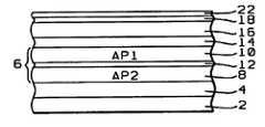
- FIG. 1 athere is shown a schematic cross-sectional view of a typical prior art configuration of a bottom spin-filter element stack having a synthetic antiferromagnetic pinned (SyAP) layer and Ta capping layer.
- said stackhas the form:
- the stackcomprises an NiCr a seed layer ( 2 ) of approximately 40 angstroms thickness, an MnPt antiferromagnetic pinning layer ( 4 ) of approximately 130 angstroms thickness, a tri-layer formation of CoFe/Ru/CoFe ( 6 ), which is a synthetic antiferromagnetic pinned (SyAP) layer formed of two CoFe ferromagnetic layers ( 8 ) and ( 10 ), exchange coupled in mutually antiparallel magnetization directions through a Ru coupling layer ( 12 ) of approximately 8 angstroms thickness.
- CoFe layer ( 8 )is denoted the second antiparallel layer, AP2, and is formed to a thickness of approximately 15 angstroms.
- CoFe layer ( 10 )is denoted the first antiparallel layer, AP1, and is formed to a thickness of approximately 20 angstroms.
- the term “antiparallel” in this contextrefers to the mutually antiparallel directions of the magnetizations of the two pinned layers that corresponds to the low energy state between AP1 and AP2 when separated by the 8 angstrom Ru layer.
- the “second” layer referred to in this contextis the one contiguous with the antiferromagnetic pinning layer ( 4 ), whereas the “first” layer ( 10 ) is the one contiguous with the subsequently deposited Cu spacer layer ( 14 ).
- Said Cu spacer layer ( 14 )is a non-magnetic spacer layer of approximately 19 angstroms thickness, separating the pinned layer ( 6 ) from the free ferromagnetic layer ( 16 ), which is a CoFe layer deposited to a thickness of approximately 20 angstroms.
- a Cu layer ( 18 ) of approximate thickness 5 angstromsis formed on the free layer and serves as an oxidation barrier and a conducting layer.
- a Ta layer ( 20 ) of approximate thickness 8 angstromsis formed on the Cu layer.
- Layers ( 18 ) and ( 20 )will be generally referred to as a capping formation for the sensor stack.
- FIG. 1 bthere is shown a schematic cross-sectional view of one preferred embodiment of a new structure, compositionally described below, formed in accord with the method of the present invention.
- the stackcomprises a giant magnetoresistive (GMR) property enhancing NiCr (or NiFeCr) seed layer ( 2 ) of approximately 40 angstroms thickness on which is formed an MnPt antiferromagnetic pinning layer ( 4 ) of approximately 130 angstroms thickness.
- GMRgiant magnetoresistive
- a tri-layer formation of CoFe/Ru/CoFe( 6 ), which is a synthetic antiferromagnetic pinned (SyAP) layer formed of two CoFe ferromagnetic layers, ( 8 ), which is AP2 and ( 10 ), which is AP1, exchange coupled in mutually antiparallel magnetization directions through a Ru coupling layer ( 12 ) of approximately 8 angstroms thickness, is formed on the MnPt pinning layer.
- SyAPsynthetic antiferromagnetic pinned
- the FeTaO capping layeris formed as an initially deposited FeTa layer which is approximately 95% Fe by number of atoms and approximately 5% Ta by number of atoms, which is subsequently oxidized to FeTaO in a PM5 TIM module under the preferred oxidation condition (OX):
- the magnetizations of the various layersare established through a three step thermal anneal in the presence of external magnetic fields as follows:
- FIG. 1 cthere is shown a schematic cross-sectional view of a second preferred embodiment of a new structure, compositionally described below, also formed in accord with the method of the present invention.
- the stackcomprises a GMR property enhancing NiCr (or NiFeCr) seed layer ( 2 ) of approximately 40 angstroms thickness on which is formed an MnPt antiferromagnetic pinning layer ( 4 ) of approximately 100 angstroms thickness.
- the synthetic pinned layer ( 7 )comprises an AP2 layer ( 9 ), which is a first layer of CoFe ( 19 ) of approximately 6.5 angstroms thickness, on which is formed a Ta layer ( 11 ) of approximately 1 angstroms thickness which increases the resistance of the AP2 layer by current shunting and thereby increases the GMR ratio, on which Ta layer is formed a second layer of CoFe ( 17 ) of approximately 6.5 angstroms thickness.
- a Ru coupling layer ( 12 )formed to a thickness of approximately 8 angstroms, separates the AP2 layer ( 9 ) from an AP1 layer ( 21 ), which is a layer of CoFe formed to a thickness of approximately 18 angstroms.
- a non-magnetic Cu spacer layer ( 14 )is formed to a thickness of approximately 19 angstroms on the AP1 layer to separate it from the ferromagnetic free layer ( 16 ), which is a layer of CoFe formed to a thickness of approximately 20 angstroms.
- a specularly reflecting FeTaO (NOL) capping layer ( 22 )is then formed on the ferromagnetically free layer.
- the FeTaO capping layeris formed as an initially deposited FeTa layer which is approximately 95% Fe by number of atoms and approximately 5% Ta by number of atoms, which is subsequently oxidized in a PM5 TIM module under the preferred oxidation condition (OX):
- the magnetizations of the various layersare established through a three step thermal anneal in the presence of external magnetic fields as follows:
- samples 1 and 3are standard reference bottom spin valves with Cu spacer layers of 19 A and 18 A thickness.
- Samples 2 and 4are bottom spin valves made in accord with the method of the present invention wherein a specularly reflecting capping layer of FeTaO is added. It can be seen from the table that the FeTaO capped samples display greatly improved values of DR/R and DR. Sample 5 displays the greatest improvement in DR/R and DR. It has also been experimentally verified that the sheet resistance of samples 2 and 4 is less than that of samples 1 and 3 .
- Sample 5differs from samples 2 and 4 in that samples 2 and 4 interpose a Cu layer between the CoFe free layer and the FeTaO capping layer, whereas sample 5 does not have such a Cu layer. Additionally, sample five interposes an approximately 1 angstrom thick layer of Ta as a resistance increasing layer within the AP2 layer which contributes to the GMR ratio improvement of that sample.
- the CoFe/FeTaO interfaceprovides better specularity than the CoFe/Cu/FeTaO interface.
- reducing the Cu spacer thickness from approximately 19 angstroms (sample 2 ) to approximately 18 angstroms (sample 4 )provided an improvement in sample 4 as compared to sample 2 . Reducing the Cu layer thickness in the reference samples, 1 and 3 , also appears to provide an improvement, but it was shown experimentally that the thinner Cu layer in the reference sample increased the interlayer coupling field to a value that was unsuitable for device applications.
Landscapes
- Engineering & Computer Science (AREA)
- Chemical & Material Sciences (AREA)
- Nanotechnology (AREA)
- Crystallography & Structural Chemistry (AREA)
- Physics & Mathematics (AREA)
- Power Engineering (AREA)
- Manufacturing & Machinery (AREA)
- Condensed Matter Physics & Semiconductors (AREA)
- General Physics & Mathematics (AREA)
- Materials Engineering (AREA)
- Mechanical Engineering (AREA)
- Metallurgy (AREA)
- Organic Chemistry (AREA)
- Spectroscopy & Molecular Physics (AREA)
- Mathematical Physics (AREA)
- Theoretical Computer Science (AREA)
- Hall/Mr Elements (AREA)
- Magnetic Heads (AREA)
- Thin Magnetic Films (AREA)
Abstract
Description
This application is related to Ser. No. 10/037,812, filing date Jan. 4, 2002, assigned to the same assignee as the present invention.
1. Field of the Invention
This invention relates generally to processes and materials used in the fabrication of a giant magnetoresistive (GMR) sensor, and more specifically to the use of a novel specularly reflecting nano-oxide layer (NOL) as a capping layer of a bottom spin valve sensor structure to improve its GMR ratio.
2. Description of the Related Art
One of the most commonly used structural configurations of magnetic and non-magnetic layers in giant magnetoresistive (GMR) read-heads is the so-called spin-valve magnetoresistive (SVMR) structure. In the most basic version of the SVMR, two ferromagnetic layers such as CoFe or NiFe are separated by a thin layer of electrically conducting but non-magnetic material such as Cu. One of the layers has its magnetization direction fixed in space or “pinned,” by exchange coupling with an antiferromagnetic (AFM) layer, usually a layer of MnPt, directly deposited upon it. The remaining ferromagnetic layer, the unpinned or free layer, can rotate its magnetization vector in response to small variations in external magnetic fields such as are produced by moving magnetic media, (which variations do not affect the magnetization direction of the pinned layer). The rotation of one magnetization relative to the other produces changes in the resistance (magnetoresistance) of the three layer structure, the changes being dependent on the cosine of the angle between the two magnetization vectors. As a result of these resistance variations, a constant “sense” current sent through the SVMR produces voltage variations across it, which are sensed by external circuitry. This effect of magnetization directions on electrical resistance is a result of spin dependent electron scattering, wherein the orientation of the electronic spins of the electrons in the sense current relative to the magnetization of the layer directly affects their scattering cross-sections and, consequently, the resistance of the magnetic material. Newer versions of the spin valve configuration make use of a pinned layer which is a triply laminated layer comprising two ferromagnetic layers magnetically exchange coupled by a thin, non-magnetic “spacer” or “coupling” layer. The two ferromagnetic layers are coupled in a manner that has their respective magnetizations maintained in antiparallel directions by the antiferromagnetic pinning layer. This type of composite pinned layer is termed a “synthetic antiferromagnetic (SyAF) pinned layer,” SyAP for brevity.
An older version of the use of variable magnetoresistance as a sensing tool was the anisotropic magnetoresistive (AMR) effect, wherein the resistance of a magnetic material was found to depend upon the angle between its magnetization and the direction of a current through it. The discovery of ways to enhance the magnetoresistive effect by the use of two layers of magnetic material (the spin valve) rather than one and by the methods used to form these layers (eg. the SyAF pinned layer), has led to what is now called the giant magnetorsistive (GMR) effect. It is this GMR which will be the subject of the present invention.
The major figure of merit for SVMR performance is its magnetoresistive ratio dR/R (usually expressed as a percentage), which is a measure of the maximum variation of its resistance that can be expected in operation. Improvements in the magnetoresistive ratio of a sensor element can be expected if the electrons in the sense current spend more time within the magnetically active portions of the sensor. For example, if the sensor element contains electrically conductive layers which do not directly contribute to the magnetoresistive effect (eg. they are not magnetic), then portions of the sense current may be shunted through these layers and not contribute to voltage variations across the sensor. It is now generally well accepted that a major contribution to the GMR effect is the presence of interfaces between various layers of the sensor elements. These interfaces produce specular reflection of the electrons, effectively removing mean-free-path limitations on electron scattering that would normally be placed on them by the external dimensions of the sensor. The realization of the importance of internal reflections on the magnetoresistive ratio, has produced great interest in the formation of sensor elements that exploit these interfacial scattering effects. For example, various types of capping layers, seed layers, buffer layers and nano-oxide layers (NOL) have been proposed as mechanisms for improving magnetorsistive ratios of sensor elements.
Huai et al. (U.S. Pat. No. 6,222,707 B1) teaches a method in which a seed layer is used to provide an improved texture for an antiferromagnetic layer grown upon it. The seed layer allows the growth of improved forms of antiferromagnetic pinning layers in bottom spin valves (spin valves in which the pinned layer is vertically beneath the free layer) thereby improving the exchange coupling between the pinning and pinned layers and, consequently, improving the magnetoresistive ratio.
Huai et al. (U.S. Pat. No. 6,175,476 B1) provides a bottom spin valve sensor having two antiparallel pinned layers coupled by a high resistivity rhenium layer that reduces shunt current through the three-piece pinned layer while still retaining adequate coupling between the two antiparallel layers. The sensor also includes a Ta capping layer whose purpose is to prevent oxidation of the sensor.
Gill (U.S. Pat. No. 6,181,534 B1) teaches a method for forming a magnetoresistive spin valve sensor element in which copper and nickel oxide specular relection layers are formed on each other and over a free magnetic layer.
Pinarbasi (U.S. Pat. No. 6,208,491 B1) teaches the formation of a capping structure comprising layers of CoFe and Ta or, alternatively CoFe, Cu and Ta, which improves the magnetoresistive performance subsequent to long periods of time at high temperatures.
Lee et al. (U.S. Pat. No. 5,731,936) teaches the formation of an MR sensor having a capping layer that can be either a Ta layer, an NiFeCr layer, an NiCr layer, an NiCr/Ta layer, or a Ta/NiCr layer. It is claimed that either the NiFeCr layer or the NiCr layer provide improved sensor thermal stability as compared to a single Ta capping layer.
Kim et al. (U.S. Pat. No. 5,637,235) provide a bottom spin valve sensor having a Ta capping layer of between 0-100 angstroms thickness to protect the upper surface of the top ferromagnetic layer.
The literature also contains reports of magnetoresistive ratio improvements as a result of the inclusion of novel materials and structures in the fabrication of sensors. In this regard, Swagten et al., in “Specular Reflections in Spin Valves Bounded by NiO Layers,” IEEE Transactions on Magnetics, Vol. 34, No. 4, July 1998, pp. 948-953, report on achieving increased electron reflectivity by an insulating NiO layer that is used to exchange bias a spin valve. Swagten et al., in “Enhanced giant magnetoresistance in spin-valves sandwiched between insulating NiO,” Phys. Rev. B, Vol. 53, No. 14, Apr. 1, 1966 also report on the enhanced GMR effects obtained when sandwiching Co/Cu/Co and Ni80Fe20/Cu/Ni80Fe20between layers of NiO.
Y. Kamiguchi et al., in “CoFe Specular Spin Valve GMR Head Using NOL in Pinned Layer,” Paper DB-01, Digest of Intermagnetic Conference 1999, report on a spin valve structure in which the pinned layer contains a nano-oxide layer (NOL) which enhances specular electron scattering.
T. Mizuguchi and H. Kano, in “Characteristics of spin-valve films with non-magnetic oxide layers for specular scattering,” Paper EB-12, Digest of MMM/Intermag. 2001 conference, p. 263, report on a new spin valve structure in which the coercivity of the free layer remains low while the GMR properties are improved. In their structure, the free layer is separated by a Cu layer from a top TaO specularly reflecting capping layer and there is another specularly reflecting RuO layer incorporated within the pinned layer.
Y. Huai et al., in “Highly Sensitive Spin-Valve Heads with Specular Thin Oxide Capping Layers,” Paper EB-14, Digest of MMM/Intermag. 2001 Conference, p. 263, discuss the specular reflection enhancing effects of thin oxide capping layers used in bottom synthetic specular spin-valve structures.
The present invention provides a method of improving the GMR ratio of a bottom spin-valve structure by the use of a novel NOL material layer as its capping layer.
It is an object of this invention is to provide a method for forming a bottom spin-valve sensor element having a higher GMR ratio and lower resistance than those formed by prior art methods.
It is a second object of this invention to provide a method of forming such a sensor that is capable of reading magnetic media on which the stored density is in the approximate range between 45 Gb/in2and 70 Gb/in2.
In accord with this object, There is provided a method for forming a bottom spin valve sensor element having a synthetic antiferromagnetic (SyAF) pinned layer and based on a NiCr magnetoresistive enhancing seed layer, said method further comprising the formation of a novel, specularly reflecting FeTaO capping layer over the element.
The objects, features and advantages of the present invention are understood within the context of the Description of the Preferred Embodiments, as set forth below. The Description of the Preferred Embodiments is understood within the context of the accompanying figure, wherein:
FIGS. 1a,1band1care schematic cross-sectional views of a bottom spin-valve sensor formed in accord with the prior art (1a) and in accord with two embodiments of the method of the present invention (1b&1c).
The present invention provides a method for fabricating a bottom spin-valve sensor element of high magnetoresistive ratio by forming a novel, specularly reflecting nano-oxide layer (NOL) as its capping layer.
Referring first to FIG. 1a, there is shown a schematic cross-sectional view of a typical prior art configuration of a bottom spin-filter element stack having a synthetic antiferromagnetic pinned (SyAP) layer and Ta capping layer. Compositionally, said stack has the form:
40A NiCr/130A MnPt/15A CoFe/8A Ru/20A CoFe/19A Cu/20A CoFe/5A Cu/8A Ta.
where “A” is angstroms.
As shown in FIG. 1a, the stack comprises an NiCr a seed layer (2) of approximately 40 angstroms thickness, an MnPt antiferromagnetic pinning layer (4) of approximately 130 angstroms thickness, a tri-layer formation of CoFe/Ru/CoFe (6), which is a synthetic antiferromagnetic pinned (SyAP) layer formed of two CoFe ferromagnetic layers (8) and (10), exchange coupled in mutually antiparallel magnetization directions through a Ru coupling layer (12) of approximately 8 angstroms thickness. CoFe layer (8) is denoted the second antiparallel layer, AP2, and is formed to a thickness of approximately 15 angstroms. CoFe layer (10) is denoted the first antiparallel layer, AP1, and is formed to a thickness of approximately 20 angstroms. The term “antiparallel” in this context refers to the mutually antiparallel directions of the magnetizations of the two pinned layers that corresponds to the low energy state between AP1 and AP2 when separated by the 8 angstrom Ru layer. The “second” layer referred to in this context is the one contiguous with the antiferromagnetic pinning layer (4), whereas the “first” layer (10) is the one contiguous with the subsequently deposited Cu spacer layer (14). Said Cu spacer layer (14) is a non-magnetic spacer layer of approximately 19 angstroms thickness, separating the pinned layer (6) from the free ferromagnetic layer (16), which is a CoFe layer deposited to a thickness of approximately 20 angstroms. A Cu layer (18) of approximate thickness 5 angstroms is formed on the free layer and serves as an oxidation barrier and a conducting layer. A Ta layer (20) ofapproximate thickness 8 angstroms is formed on the Cu layer. Layers (18) and (20) will be generally referred to as a capping formation for the sensor stack.
Referring next to FIG. 1b, there is shown a schematic cross-sectional view of one preferred embodiment of a new structure, compositionally described below, formed in accord with the method of the present invention.
40A NiCr/130A MnPt/15A CoFe/8A Ru/20A CoFe/19A Cu/20A CoFe/5A Cu/5A FeTa//OX.
As is shown schematically in FIG. 1b, the stack comprises a giant magnetoresistive (GMR) property enhancing NiCr (or NiFeCr) seed layer (2) of approximately 40 angstroms thickness on which is formed an MnPt antiferromagnetic pinning layer (4) of approximately 130 angstroms thickness. A tri-layer formation of CoFe/Ru/CoFe (6), which is a synthetic antiferromagnetic pinned (SyAP) layer formed of two CoFe ferromagnetic layers, (8), which is AP2 and (10), which is AP1, exchange coupled in mutually antiparallel magnetization directions through a Ru coupling layer (12) of approximately 8 angstroms thickness, is formed on the MnPt pinning layer. The AP1 and AP2 terminology is the same as that used in describing FIG. 1a. A Cu layer (14), which is a metallic, non-magnetic spacer layer of approximately 19 angstroms thickness, is formed on the AP1 (10) layer of the pinned layer, separating the pinned layer (6) from the free ferromagnetic layer (16), which is a CoFe layer deposited to a thickness of approximately 20 angstroms. A Cu layer (18) of approximate thickness 5 angstroms is formed on the free layer. On this Cu layer (18), there is then formed a specularly reflecting capping layer (NOL) of FeTaO (22) of approximately 5 angstroms thickness. The FeTaO capping layer is formed as an initially deposited FeTa layer which is approximately 95% Fe by number of atoms and approximately 5% Ta by number of atoms, which is subsequently oxidized to FeTaO in a PM5 TIM module under the preferred oxidation condition (OX):
OX: 5 sccm O2flow rate (0.05 mTorr)×10 sec.
It has also been determined that similar advantageous results are obtained when the oxidized FeTa layer is replaced by a similarly oxidized Fe or oxidized (Fe65Co35)97V3layer.
Subsequent to the formation of the element as above, the magnetizations of the various layers are established through a three step thermal anneal in the presence of external magnetic fields as follows:
1: 270° C./1 kOe/10 min., for the free layer, longitudinal field.
2: 270° C./8 kOe/3 hr., for the pinned layer, with the field being in the transverse direction.
3: 210° C./200 Oe/2 hr., for the free layer, longitudinal field.
Referring finally to FIG. 1c, there is shown a schematic cross-sectional view of a second preferred embodiment of a new structure, compositionally described below, also formed in accord with the method of the present invention.
40A NiCr/100A MnPt/6.5A CoFe/Ta1A/6.5A CoFe/8A Ru/18A CoFe/19A Cu/20A CoFe/5A FeTa//OX.
As is shown schematically in FIG. 1c, the stack comprises a GMR property enhancing NiCr (or NiFeCr) seed layer (2) of approximately 40 angstroms thickness on which is formed an MnPt antiferromagnetic pinning layer (4) of approximately 100 angstroms thickness. A five-layer formation of CoFe/Ta1/CoFe/Ru/CoFe (7), which is a synthetic antiferromagnetic pinned (SyAP) layer, is formed on the MnPt layer. The synthetic pinned layer (7) comprises an AP2 layer (9), which is a first layer of CoFe (19) of approximately 6.5 angstroms thickness, on which is formed a Ta layer (11) of approximately 1 angstroms thickness which increases the resistance of the AP2 layer by current shunting and thereby increases the GMR ratio, on which Ta layer is formed a second layer of CoFe (17) of approximately 6.5 angstroms thickness. A Ru coupling layer (12) formed to a thickness of approximately 8 angstroms, separates the AP2 layer (9) from an AP1 layer (21), which is a layer of CoFe formed to a thickness of approximately 18 angstroms. A non-magnetic Cu spacer layer (14) is formed to a thickness of approximately 19 angstroms on the AP1 layer to separate it from the ferromagnetic free layer (16), which is a layer of CoFe formed to a thickness of approximately 20 angstroms. A specularly reflecting FeTaO (NOL) capping layer (22) is then formed on the ferromagnetically free layer. The FeTaO capping layer is formed as an initially deposited FeTa layer which is approximately 95% Fe by number of atoms and approximately 5% Ta by number of atoms, which is subsequently oxidized in a PM5 TIM module under the preferred oxidation condition (OX):
OX: 5 sccm O2flow rate (0.05 mTorr)×10 sec.
Subsequent to the formation of the element as above, the magnetizations of the various layers are established through a three step thermal anneal in the presence of external magnetic fields as follows:
1: 270° C./1 kOe/10 min., for the free layer, longitudinally directed field.
2: 270° C./8 kOe/3 hr., for the pinned layer, with the field being in the transverse direction.
3: 210° C./200 Oe/2 hr., for the free layer, longitudinally directed field.
Experiments performed on sensor stacks formed in accord with the methods of the prior art and on sensor stacks formed in accord with the method of the present invention show a distinct improvement in the magnetoresistive properties of the latter stacks as compared with the former. Table 1 below compares DR/R and DR for a reference prior art stack and stacks formed using the method of the present invention for each of the three oxidation processes described above.
| TABLE 1 | |||
| DR/R (%) | DR (Ohm/sq) | ||
| 1: NiCr40/MnPt130/CoFe15/Ru8/CoFe20/Cu19/CoFe20/Cu5/Ta8 | 16.95 | 3.02 |
| 2: NiCr40/MnPt130/CoFe15/Ru8/CoFe20/Cu19/CoFe20/Cu5/FeTa//OX | 17.75 | 3.04 |
| 3: NiCr40/MnPt130/CoFe15/Ru8/CoFe20/Cu18/CoFe20/Cu5/Ta8 | 17.59 | 3.21 |
| 4: NiCr40/MnPt130/CoFe15/Ru8/CoFe20/Cu18/CoFe20/Cu5/FeTa//OX | 18.08 | 3.15 |
| 5: NiCr40/MnPt100/CoFe6.5/Ta1/CoFe6.5/Ru8/CoFe18/Cu19/CoFe20/FeTa//OX | 19.38 | 3.86 |
All numerical values in the stack formations above are in angstroms. In table 1,samples 1 and3 are standard reference bottom spin valves with Cu spacer layers of 19 A and 18 A thickness.Samples samples samples 1 and3. Sample5 differs fromsamples samples sample 4 as compared tosample 2. Reducing the Cu layer thickness in the reference samples,1 and3, also appears to provide an improvement, but it was shown experimentally that the thinner Cu layer in the reference sample increased the interlayer coupling field to a value that was unsuitable for device applications.
As is understood by a person skilled in the art, the preferred embodiment of the present invention is illustrative of the present invention rather than limiting of the present invention. Revisions and modifications may be made to methods, materials, structures and dimensions employed in practicing the method of the present invention, while still remaining in accord with the spirit and scope of the present invention as defined by the appended claims.
Claims (11)
1. A method for forming a bottom spin valve magnetorestive sensor element comprising:
providing a substrate;
forming on the substrate a magnetoresistive-property-enhancing seed layer;
forming on said seed layer a pinning layer of antiferromagnetic material;
forming on said pinning layer a synthetic antiferromagnetic pinned (SyAP) layer, said formation further comprising:
forming on said pinning layer a second antiparallel (AP2) pinned layer of ferromagnetic material;
forming on said second antiparallel (AP2) pinned layer a non-magnetic coupling layer; and
forming on said non-magnetic coupling layer a first antiparallel (AP1) pinned layer to complete said SyAP layer;
forming on said first antiparallel (AP1) layer of said SyAP layer a non-magnetic spacer layer;
forming on said non-magnetic spacer layer a ferromagnetic free layer;
forming on said ferromagnetic free layer a double-layer capping layer, said capping layer comprising a first layer of non-magnetic material on which is formed a second layer of the specularly reflecting material oxidized FeTa, oxidized Fe or oxidized (Fe65Co35)97V3;
thermally annealing said sensor element at a prescribed succession of temperatures in the presence of a corresponding sequence of external magnetic fields, establishing, thereby, the magnetizations of said free and said pinned magnetic layers.
2. The method ofclaim 1 wherein the non-magnetic material layer of the capping layer is a layer of non-magnetic material chosen from the group consisting of Cu, Ag, Au, Rh and Ru.
3. The method ofclaim 2 wherein the non-magnetic material layer of the capping layer is a layer of Cu formed to a thickness of between approximately 0 and 20 angstroms.
4. The method ofclaim 1 wherein the specularly reflecting layer of the capping layer is a layer of FeTaO formed to a thickness of between approximately 5 and 40 angstroms.
5. The method ofclaim 4 wherein the specularly reflecting layer of FeTaO is formed by an oxidation process applied to a layer of FeTa deposited on said non-magnetic material layer to a thickness of between approximately 3 and 30 angstroms.
6. The method ofclaim 5 wherein said layer of deposited FeTa is a layer which is approximately 95% Fe by number of atoms and approximately 5% Ta by number of atoms.
7. The method ofclaim 6 wherein said oxidation process is carried out in a PM5 TIM module in which there is supplied molecular oxygen at a flow rate of between approximately 5 and 50 sccm, a pressure of between approximately 0.05 and 0.5 mTorr for a time duration of between approximately 9 and 11 seconds, but where approximately 10 seconds is preferred.
8. The method ofclaim 1 wherein said specularly reflecting capping layer of oxidized Fe or oxidized (Fe65Co35)97V3is formed to a thickness of between approximately 5 and 40 angstroms.
9. The method ofclaim 8 wherein said oxidation process is carried out in a PM5 TIM module in which there is supplied molecular oxygen at a flow rate of between approximately 5 and 50 sccm, a pressure of between approximately 0.05 and 0.5 mTorr for a time duration of between approximately 9 and 11 seconds, but where approximately 10 seconds is preferred.
10. A method for forming a bottom spin valve magnetorestive sensor element comprising:
providing a substrate;
forming on the substrate a magnetoresistive-property-enhancing seed layer;
forming on said seed layer a pinning layer of antiferromagnetic material;
forming on said pinning layer a synthetic antiferromagnetic pinned (SyAP) layer, said formation further comprising:
forming on said pinning layer a second antiparallel (AP2) pinned layer of ferromagnetic material;
forming on said second antiparallel (AP2) pinned layer a non-magnetic coupling layer; and
forming on said non-magnetic coupling layer a first antiparallel (AP1) pinned layer to complete said SyAP layer;
forming on said first antiparallel (AP1) layer of said SyAP layer a non-magnetic spacer layer;
forming on said non-magnetic spacer layer a ferromagnetic free layer;
forming on said ferromagnetic free layer a capping layer of the specularly reflecting material oxidized FeTa;
thermally annealing said sensor element at a prescribed succession of temperatures in the presence of a corresponding sequence of external magnetic fields, establishing, thereby, the magnetizations of said free and said pinned magnetic layers.
11. The method ofclaim 10 wherein said specularly reflecting capping layer is a layer of FeTaO formed to a thickness of between approximately 5 and 40 angstroms.
Priority Applications (3)
| Application Number | Priority Date | Filing Date | Title |
|---|---|---|---|
| US10/050,644US6773515B2 (en) | 2002-01-16 | 2002-01-16 | FeTa nano-oxide layer as a capping layer for enhancement of giant magnetoresistance in bottom spin valve structures |
| JP2003008085AJP4421822B2 (en) | 2002-01-16 | 2003-01-16 | Bottom spin valve magnetoresistive sensor element and manufacturing method thereof |
| US10/856,180US7262941B2 (en) | 2002-01-16 | 2004-05-28 | FeTa nano-oxide layer as a capping layer for enhancement of giant magnetoresistance in bottom spin valve structures |
Applications Claiming Priority (1)
| Application Number | Priority Date | Filing Date | Title |
|---|---|---|---|
| US10/050,644US6773515B2 (en) | 2002-01-16 | 2002-01-16 | FeTa nano-oxide layer as a capping layer for enhancement of giant magnetoresistance in bottom spin valve structures |
Related Child Applications (1)
| Application Number | Title | Priority Date | Filing Date |
|---|---|---|---|
| US10/856,180DivisionUS7262941B2 (en) | 2002-01-16 | 2004-05-28 | FeTa nano-oxide layer as a capping layer for enhancement of giant magnetoresistance in bottom spin valve structures |
Publications (2)
| Publication Number | Publication Date |
|---|---|
| US20030133232A1 US20030133232A1 (en) | 2003-07-17 |
| US6773515B2true US6773515B2 (en) | 2004-08-10 |
Family
ID=21966477
Family Applications (2)
| Application Number | Title | Priority Date | Filing Date |
|---|---|---|---|
| US10/050,644Expired - Fee RelatedUS6773515B2 (en) | 2002-01-16 | 2002-01-16 | FeTa nano-oxide layer as a capping layer for enhancement of giant magnetoresistance in bottom spin valve structures |
| US10/856,180Expired - Fee RelatedUS7262941B2 (en) | 2002-01-16 | 2004-05-28 | FeTa nano-oxide layer as a capping layer for enhancement of giant magnetoresistance in bottom spin valve structures |
Family Applications After (1)
| Application Number | Title | Priority Date | Filing Date |
|---|---|---|---|
| US10/856,180Expired - Fee RelatedUS7262941B2 (en) | 2002-01-16 | 2004-05-28 | FeTa nano-oxide layer as a capping layer for enhancement of giant magnetoresistance in bottom spin valve structures |
Country Status (2)
| Country | Link |
|---|---|
| US (2) | US6773515B2 (en) |
| JP (1) | JP4421822B2 (en) |
Cited By (88)
| Publication number | Priority date | Publication date | Assignee | Title |
|---|---|---|---|---|
| US20030192168A1 (en)* | 2002-01-04 | 2003-10-16 | Headway Technologies, Inc. | FeTa nano-oxide layer in pinned layer for enhancement of giant magnetoresistance in bottom spin valve structures |
| US20040223266A1 (en)* | 2002-01-16 | 2004-11-11 | Headway Technologies, Inc. | FeTa nano-oxide layer as a capping layer for enhancement of giant magnetoresistance in bottom spin valve structures |
| US20050041339A1 (en)* | 2002-04-17 | 2005-02-24 | Headway Technologies, Inc. | Structure and process to fabricate lead overlay (LOL) on the bottom spin valve |
| US20080112094A1 (en)* | 2003-08-19 | 2008-05-15 | New York University | High speed low power annular magnetic devices based on current induced spin-momentum transfer |
| US20080226948A1 (en)* | 2007-03-12 | 2008-09-18 | Tomohito Mizuno | Magneto-resistance effect element having diffusion blocking layer and thin-film magnetic head |
| US20090296462A1 (en)* | 2003-08-19 | 2009-12-03 | New York University | High speed low power magnetic devices based on current induced spin-momentum transfer |
| US7994596B2 (en) | 2004-01-20 | 2011-08-09 | Headway Technologies, Inc. | Magnetic tunneling junction film structure with process determined in-plane magnetic anisotropy |
| US20120129007A1 (en)* | 2010-11-22 | 2012-05-24 | Headway Technologies, Inc. | Fabrication of a coercivity hard bias using FePt containing film |
| US8755222B2 (en) | 2003-08-19 | 2014-06-17 | New York University | Bipolar spin-transfer switching |
| US8982613B2 (en) | 2013-06-17 | 2015-03-17 | New York University | Scalable orthogonal spin transfer magnetic random access memory devices with reduced write error rates |
| US9082888B2 (en) | 2012-10-17 | 2015-07-14 | New York University | Inverted orthogonal spin transfer layer stack |
| US9082950B2 (en) | 2012-10-17 | 2015-07-14 | New York University | Increased magnetoresistance in an inverted orthogonal spin transfer layer stack |
| US9263667B1 (en) | 2014-07-25 | 2016-02-16 | Spin Transfer Technologies, Inc. | Method for manufacturing MTJ memory device |
| US9337412B2 (en) | 2014-09-22 | 2016-05-10 | Spin Transfer Technologies, Inc. | Magnetic tunnel junction structure for MRAM device |
| US9728712B2 (en) | 2015-04-21 | 2017-08-08 | Spin Transfer Technologies, Inc. | Spin transfer torque structure for MRAM devices having a spin current injection capping layer |
| US9741926B1 (en) | 2016-01-28 | 2017-08-22 | Spin Transfer Technologies, Inc. | Memory cell having magnetic tunnel junction and thermal stability enhancement layer |
| US9773974B2 (en) | 2015-07-30 | 2017-09-26 | Spin Transfer Technologies, Inc. | Polishing stop layer(s) for processing arrays of semiconductor elements |
| US9812184B2 (en) | 2007-10-31 | 2017-11-07 | New York University | Current induced spin-momentum transfer stack with dual insulating layers |
| US9853206B2 (en) | 2015-06-16 | 2017-12-26 | Spin Transfer Technologies, Inc. | Precessional spin current structure for MRAM |
| US10032978B1 (en) | 2017-06-27 | 2018-07-24 | Spin Transfer Technologies, Inc. | MRAM with reduced stray magnetic fields |
| US20180328902A1 (en)* | 2017-05-12 | 2018-11-15 | National Chiao Tung University | Hydrogen sensing device |
| US10141499B1 (en) | 2017-12-30 | 2018-11-27 | Spin Transfer Technologies, Inc. | Perpendicular magnetic tunnel junction device with offset precessional spin current layer |
| US10163479B2 (en) | 2015-08-14 | 2018-12-25 | Spin Transfer Technologies, Inc. | Method and apparatus for bipolar memory write-verify |
| US10199083B1 (en) | 2017-12-29 | 2019-02-05 | Spin Transfer Technologies, Inc. | Three-terminal MRAM with ac write-assist for low read disturb |
| US10229724B1 (en) | 2017-12-30 | 2019-03-12 | Spin Memory, Inc. | Microwave write-assist in series-interconnected orthogonal STT-MRAM devices |
| US10236048B1 (en) | 2017-12-29 | 2019-03-19 | Spin Memory, Inc. | AC current write-assist in orthogonal STT-MRAM |
| US10236439B1 (en) | 2017-12-30 | 2019-03-19 | Spin Memory, Inc. | Switching and stability control for perpendicular magnetic tunnel junction device |
| US10236047B1 (en) | 2017-12-29 | 2019-03-19 | Spin Memory, Inc. | Shared oscillator (STNO) for MRAM array write-assist in orthogonal STT-MRAM |
| US10255962B1 (en) | 2017-12-30 | 2019-04-09 | Spin Memory, Inc. | Microwave write-assist in orthogonal STT-MRAM |
| US10270027B1 (en) | 2017-12-29 | 2019-04-23 | Spin Memory, Inc. | Self-generating AC current assist in orthogonal STT-MRAM |
| US10319900B1 (en) | 2017-12-30 | 2019-06-11 | Spin Memory, Inc. | Perpendicular magnetic tunnel junction device with precessional spin current layer having a modulated moment density |
| US10339993B1 (en) | 2017-12-30 | 2019-07-02 | Spin Memory, Inc. | Perpendicular magnetic tunnel junction device with skyrmionic assist layers for free layer switching |
| US10360961B1 (en) | 2017-12-29 | 2019-07-23 | Spin Memory, Inc. | AC current pre-charge write-assist in orthogonal STT-MRAM |
| US10360964B2 (en) | 2016-09-27 | 2019-07-23 | Spin Memory, Inc. | Method of writing contents in memory during a power up sequence using a dynamic redundancy register in a memory device |
| US10360962B1 (en) | 2017-12-28 | 2019-07-23 | Spin Memory, Inc. | Memory array with individually trimmable sense amplifiers |
| US10366775B2 (en) | 2016-09-27 | 2019-07-30 | Spin Memory, Inc. | Memory device using levels of dynamic redundancy registers for writing a data word that failed a write operation |
| US10367139B2 (en) | 2017-12-29 | 2019-07-30 | Spin Memory, Inc. | Methods of manufacturing magnetic tunnel junction devices |
| US10388861B1 (en) | 2018-03-08 | 2019-08-20 | Spin Memory, Inc. | Magnetic tunnel junction wafer adaptor used in magnetic annealing furnace and method of using the same |
| US10395711B2 (en) | 2017-12-28 | 2019-08-27 | Spin Memory, Inc. | Perpendicular source and bit lines for an MRAM array |
| US10395712B2 (en) | 2017-12-28 | 2019-08-27 | Spin Memory, Inc. | Memory array with horizontal source line and sacrificial bitline per virtual source |
| US10411185B1 (en) | 2018-05-30 | 2019-09-10 | Spin Memory, Inc. | Process for creating a high density magnetic tunnel junction array test platform |
| US10424726B2 (en) | 2017-12-28 | 2019-09-24 | Spin Memory, Inc. | Process for improving photoresist pillar adhesion during MRAM fabrication |
| US10424723B2 (en) | 2017-12-29 | 2019-09-24 | Spin Memory, Inc. | Magnetic tunnel junction devices including an optimization layer |
| US10438995B2 (en) | 2018-01-08 | 2019-10-08 | Spin Memory, Inc. | Devices including magnetic tunnel junctions integrated with selectors |
| US10437723B2 (en) | 2016-09-27 | 2019-10-08 | Spin Memory, Inc. | Method of flushing the contents of a dynamic redundancy register to a secure storage area during a power down in a memory device |
| US10437491B2 (en) | 2016-09-27 | 2019-10-08 | Spin Memory, Inc. | Method of processing incomplete memory operations in a memory device during a power up sequence and a power down sequence using a dynamic redundancy register |
| US10438996B2 (en) | 2018-01-08 | 2019-10-08 | Spin Memory, Inc. | Methods of fabricating magnetic tunnel junctions integrated with selectors |
| US10446210B2 (en) | 2016-09-27 | 2019-10-15 | Spin Memory, Inc. | Memory instruction pipeline with a pre-read stage for a write operation for reducing power consumption in a memory device that uses dynamic redundancy registers |
| US10446744B2 (en) | 2018-03-08 | 2019-10-15 | Spin Memory, Inc. | Magnetic tunnel junction wafer adaptor used in magnetic annealing furnace and method of using the same |
| US10460781B2 (en) | 2016-09-27 | 2019-10-29 | Spin Memory, Inc. | Memory device with a dual Y-multiplexer structure for performing two simultaneous operations on the same row of a memory bank |
| US10468588B2 (en) | 2018-01-05 | 2019-11-05 | Spin Memory, Inc. | Perpendicular magnetic tunnel junction device with skyrmionic enhancement layers for the precessional spin current magnetic layer |
| US10468590B2 (en) | 2015-04-21 | 2019-11-05 | Spin Memory, Inc. | High annealing temperature perpendicular magnetic anisotropy structure for magnetic random access memory |
| US10481976B2 (en) | 2017-10-24 | 2019-11-19 | Spin Memory, Inc. | Forcing bits as bad to widen the window between the distributions of acceptable high and low resistive bits thereby lowering the margin and increasing the speed of the sense amplifiers |
| US10489245B2 (en) | 2017-10-24 | 2019-11-26 | Spin Memory, Inc. | Forcing stuck bits, waterfall bits, shunt bits and low TMR bits to short during testing and using on-the-fly bit failure detection and bit redundancy remapping techniques to correct them |
| US10516094B2 (en) | 2017-12-28 | 2019-12-24 | Spin Memory, Inc. | Process for creating dense pillars using multiple exposures for MRAM fabrication |
| US10529439B2 (en) | 2017-10-24 | 2020-01-07 | Spin Memory, Inc. | On-the-fly bit failure detection and bit redundancy remapping techniques to correct for fixed bit defects |
| US10529915B2 (en) | 2018-03-23 | 2020-01-07 | Spin Memory, Inc. | Bit line structures for three-dimensional arrays with magnetic tunnel junction devices including an annular free magnetic layer and a planar reference magnetic layer |
| US10546625B2 (en) | 2016-09-27 | 2020-01-28 | Spin Memory, Inc. | Method of optimizing write voltage based on error buffer occupancy |
| US10546624B2 (en) | 2017-12-29 | 2020-01-28 | Spin Memory, Inc. | Multi-port random access memory |
| US10559338B2 (en) | 2018-07-06 | 2020-02-11 | Spin Memory, Inc. | Multi-bit cell read-out techniques |
| US10580827B1 (en) | 2018-11-16 | 2020-03-03 | Spin Memory, Inc. | Adjustable stabilizer/polarizer method for MRAM with enhanced stability and efficient switching |
| US10593396B2 (en) | 2018-07-06 | 2020-03-17 | Spin Memory, Inc. | Multi-bit cell read-out techniques for MRAM cells with mixed pinned magnetization orientations |
| US10600478B2 (en) | 2018-07-06 | 2020-03-24 | Spin Memory, Inc. | Multi-bit cell read-out techniques for MRAM cells with mixed pinned magnetization orientations |
| US10628316B2 (en) | 2016-09-27 | 2020-04-21 | Spin Memory, Inc. | Memory device with a plurality of memory banks where each memory bank is associated with a corresponding memory instruction pipeline and a dynamic redundancy register |
| US10650875B2 (en) | 2018-08-21 | 2020-05-12 | Spin Memory, Inc. | System for a wide temperature range nonvolatile memory |
| US10656994B2 (en) | 2017-10-24 | 2020-05-19 | Spin Memory, Inc. | Over-voltage write operation of tunnel magnet-resistance (“TMR”) memory device and correcting failure bits therefrom by using on-the-fly bit failure detection and bit redundancy remapping techniques |
| US10665777B2 (en) | 2017-02-28 | 2020-05-26 | Spin Memory, Inc. | Precessional spin current structure with non-magnetic insertion layer for MRAM |
| US10672976B2 (en) | 2017-02-28 | 2020-06-02 | Spin Memory, Inc. | Precessional spin current structure with high in-plane magnetization for MRAM |
| US10679685B2 (en) | 2017-12-27 | 2020-06-09 | Spin Memory, Inc. | Shared bit line array architecture for magnetoresistive memory |
| US10692569B2 (en) | 2018-07-06 | 2020-06-23 | Spin Memory, Inc. | Read-out techniques for multi-bit cells |
| US10699761B2 (en) | 2018-09-18 | 2020-06-30 | Spin Memory, Inc. | Word line decoder memory architecture |
| US10784439B2 (en) | 2017-12-29 | 2020-09-22 | Spin Memory, Inc. | Precessional spin current magnetic tunnel junction devices and methods of manufacture |
| US10784437B2 (en) | 2018-03-23 | 2020-09-22 | Spin Memory, Inc. | Three-dimensional arrays with MTJ devices including a free magnetic trench layer and a planar reference magnetic layer |
| US10811594B2 (en) | 2017-12-28 | 2020-10-20 | Spin Memory, Inc. | Process for hard mask development for MRAM pillar formation using photolithography |
| US10818331B2 (en) | 2016-09-27 | 2020-10-27 | Spin Memory, Inc. | Multi-chip module for MRAM devices with levels of dynamic redundancy registers |
| US10840436B2 (en) | 2017-12-29 | 2020-11-17 | Spin Memory, Inc. | Perpendicular magnetic anisotropy interface tunnel junction devices and methods of manufacture |
| US10840439B2 (en) | 2017-12-29 | 2020-11-17 | Spin Memory, Inc. | Magnetic tunnel junction (MTJ) fabrication methods and systems |
| US10886330B2 (en) | 2017-12-29 | 2021-01-05 | Spin Memory, Inc. | Memory device having overlapping magnetic tunnel junctions in compliance with a reference pitch |
| US10891997B2 (en) | 2017-12-28 | 2021-01-12 | Spin Memory, Inc. | Memory array with horizontal source line and a virtual source line |
| US10971680B2 (en) | 2018-10-01 | 2021-04-06 | Spin Memory, Inc. | Multi terminal device stack formation methods |
| US10991410B2 (en) | 2016-09-27 | 2021-04-27 | Spin Memory, Inc. | Bi-polar write scheme |
| US11107979B2 (en) | 2018-12-28 | 2021-08-31 | Spin Memory, Inc. | Patterned silicide structures and methods of manufacture |
| US11107978B2 (en) | 2018-03-23 | 2021-08-31 | Spin Memory, Inc. | Methods of manufacturing three-dimensional arrays with MTJ devices including a free magnetic trench layer and a planar reference magnetic layer |
| US11107974B2 (en) | 2018-03-23 | 2021-08-31 | Spin Memory, Inc. | Magnetic tunnel junction devices including a free magnetic trench layer and a planar reference magnetic layer |
| US11119936B2 (en) | 2016-09-27 | 2021-09-14 | Spin Memory, Inc. | Error cache system with coarse and fine segments for power optimization |
| US11119910B2 (en) | 2016-09-27 | 2021-09-14 | Spin Memory, Inc. | Heuristics for selecting subsegments for entry in and entry out operations in an error cache system with coarse and fine grain segments |
| US11151042B2 (en) | 2016-09-27 | 2021-10-19 | Integrated Silicon Solution, (Cayman) Inc. | Error cache segmentation for power reduction |
| US11621293B2 (en) | 2018-10-01 | 2023-04-04 | Integrated Silicon Solution, (Cayman) Inc. | Multi terminal device stack systems and methods |
Families Citing this family (21)
| Publication number | Priority date | Publication date | Assignee | Title |
|---|---|---|---|---|
| JP4130875B2 (en)* | 2002-06-03 | 2008-08-06 | 富士通株式会社 | Manufacturing method of spin valve reproducing head |
| US7007373B2 (en)* | 2002-11-18 | 2006-03-07 | Hitachi Global Storage Technologies Netherlands B.V. | Method of manufacturing enhanced spin-valve sensor with engineered overlayer |
| US6865109B2 (en)* | 2003-06-06 | 2005-03-08 | Seagate Technology Llc | Magnetic random access memory having flux closure for the free layer and spin transfer write mechanism |
| JP2005079487A (en)* | 2003-09-03 | 2005-03-24 | Fujitsu Ltd | Magnetoresistive film and magnetoresistive head and solid-state memory using the same |
| JP2005101441A (en)* | 2003-09-26 | 2005-04-14 | Anelva Corp | Magnetoresistive multilayer film |
| JP2005268570A (en)* | 2004-03-19 | 2005-09-29 | Alps Electric Co Ltd | Magnetic detector |
| KR100604976B1 (en) | 2004-09-03 | 2006-07-28 | 학교법인연세대학교 | Water-soluble nanoparticles stabilized with multifunctional ligands |
| KR100713745B1 (en)* | 2006-02-27 | 2007-05-07 | 연세대학교 산학협력단 | Water-soluble magnetic or metal oxide nanoparticles coated with a phase transfer ligand and a method for preparing the same |
| JP5041829B2 (en)* | 2007-03-05 | 2012-10-03 | アルプス電気株式会社 | Tunnel type magnetic sensor |
| US8018691B2 (en)* | 2008-10-20 | 2011-09-13 | Hitachi Global Storage Technologies Netherlands B.V. | CPP dual free layer magnetoresistive head for magnetic data storage |
| WO2010143718A1 (en) | 2009-06-12 | 2010-12-16 | アルプス・グリーンデバイス株式会社 | Magnetic balance current sensor |
| JP5572208B2 (en) | 2010-03-12 | 2014-08-13 | アルプス電気株式会社 | Magnetic sensor and magnetic balance type current sensor using the same |
| JP5594915B2 (en)* | 2010-03-12 | 2014-09-24 | アルプス・グリーンデバイス株式会社 | Current sensor |
| JP5487402B2 (en) | 2010-08-23 | 2014-05-07 | アルプス・グリーンデバイス株式会社 | Magnetic balanced current sensor |
| KR102078849B1 (en)* | 2013-03-11 | 2020-02-18 | 삼성전자 주식회사 | Magnetoresistive structure, Magnetic Random Access Memory device and Manufacturing Method of the same |
| JP6215001B2 (en)* | 2013-10-24 | 2017-10-18 | 日本電産サンキョー株式会社 | Magnetoresistive element, magnetic sensor device, and method of manufacturing magnetoresistive element |
| WO2015062174A1 (en)* | 2013-11-01 | 2015-05-07 | 中国科学院物理研究所 | Nanometre magnetic multilayer film for temperature sensor and manufacturing method therefor |
| US9171559B1 (en)* | 2014-09-15 | 2015-10-27 | Seagate Technology Llc | Sensor structure with pinned stabilization layer |
| US10636964B2 (en)* | 2018-03-30 | 2020-04-28 | Applied Materials, Inc. | Magnetic tunnel junctions with tunable high perpendicular magnetic anisotropy |
| US10944050B2 (en)* | 2018-05-08 | 2021-03-09 | Applied Materials, Inc. | Magnetic tunnel junction structures and methods of manufacture thereof |
| JP7202267B2 (en)* | 2019-08-06 | 2023-01-11 | 株式会社日立ハイテク | Magnetoresistive element and magnetoresistive device |
Citations (7)
| Publication number | Priority date | Publication date | Assignee | Title |
|---|---|---|---|---|
| US5637235A (en) | 1995-03-09 | 1997-06-10 | Quantum Peripherals Colorado, Inc. | Shaped spin valve type magnetoresistive transducer and method for fabricating the same incorporating domain stabilization technique |
| US5731936A (en) | 1996-09-26 | 1998-03-24 | International Business Machines Corporation | Magnetoresistive (MR) sensor with coefficient enhancing that promotes thermal stability |
| US6175476B1 (en) | 1998-08-18 | 2001-01-16 | Read-Rite Corporation | Synthetic spin-valve device having high resistivity anti parallel coupling layer |
| US6181534B1 (en) | 1998-11-09 | 2001-01-30 | International Business Machines Corporation | Antiparallel (AP) pinned spin valve sensor with specular reflection of conduction electrons |
| US6208491B1 (en) | 1999-05-26 | 2001-03-27 | International Business Machines Corporation | Spin valve with improved capping layer structure |
| US6222707B1 (en) | 1998-12-28 | 2001-04-24 | Read-Rite Corporation | Bottom or dual spin valve having a seed layer that results in an improved antiferromagnetic layer |
| US6268985B1 (en)* | 1999-03-30 | 2001-07-31 | International Business Machines Corporation | Read head having spin valve sensor with improved capping layer |
Family Cites Families (8)
| Publication number | Priority date | Publication date | Assignee | Title |
|---|---|---|---|---|
| US6556390B1 (en)* | 1999-10-28 | 2003-04-29 | Seagate Technology Llc | Spin valve sensors with an oxide layer utilizing electron specular scattering effect |
| US6407890B1 (en)* | 2000-02-08 | 2002-06-18 | International Business Machines Corporation | Dual spin valve sensor read head with a specular reflector film embedded in each antiparallel (AP) pinned layer next to a spacer layer |
| US6466418B1 (en)* | 2000-02-11 | 2002-10-15 | Headway Technologies, Inc. | Bottom spin valves with continuous spacer exchange (or hard) bias |
| US6700753B2 (en)* | 2000-04-12 | 2004-03-02 | Seagate Technology Llc | Spin valve structures with specular reflection layers |
| US6853520B2 (en)* | 2000-09-05 | 2005-02-08 | Kabushiki Kaisha Toshiba | Magnetoresistance effect element |
| US6654211B2 (en)* | 2001-04-06 | 2003-11-25 | International Business Machines Corporation | Read head including a spin valve sensor with a specular reflecting cap layer structure |
| US6581272B1 (en)* | 2002-01-04 | 2003-06-24 | Headway Technologies, Inc. | Method for forming a bottom spin valve magnetoresistive sensor element |
| US6773515B2 (en)* | 2002-01-16 | 2004-08-10 | Headway Technologies, Inc. | FeTa nano-oxide layer as a capping layer for enhancement of giant magnetoresistance in bottom spin valve structures |
- 2002
- 2002-01-16USUS10/050,644patent/US6773515B2/ennot_activeExpired - Fee Related
- 2003
- 2003-01-16JPJP2003008085Apatent/JP4421822B2/ennot_activeExpired - Fee Related
- 2004
- 2004-05-28USUS10/856,180patent/US7262941B2/ennot_activeExpired - Fee Related
Patent Citations (7)
| Publication number | Priority date | Publication date | Assignee | Title |
|---|---|---|---|---|
| US5637235A (en) | 1995-03-09 | 1997-06-10 | Quantum Peripherals Colorado, Inc. | Shaped spin valve type magnetoresistive transducer and method for fabricating the same incorporating domain stabilization technique |
| US5731936A (en) | 1996-09-26 | 1998-03-24 | International Business Machines Corporation | Magnetoresistive (MR) sensor with coefficient enhancing that promotes thermal stability |
| US6175476B1 (en) | 1998-08-18 | 2001-01-16 | Read-Rite Corporation | Synthetic spin-valve device having high resistivity anti parallel coupling layer |
| US6181534B1 (en) | 1998-11-09 | 2001-01-30 | International Business Machines Corporation | Antiparallel (AP) pinned spin valve sensor with specular reflection of conduction electrons |
| US6222707B1 (en) | 1998-12-28 | 2001-04-24 | Read-Rite Corporation | Bottom or dual spin valve having a seed layer that results in an improved antiferromagnetic layer |
| US6268985B1 (en)* | 1999-03-30 | 2001-07-31 | International Business Machines Corporation | Read head having spin valve sensor with improved capping layer |
| US6208491B1 (en) | 1999-05-26 | 2001-03-27 | International Business Machines Corporation | Spin valve with improved capping layer structure |
Non-Patent Citations (5)
| Title |
|---|
| J.C.S. Kools, et al., "Magnetic Properties of Specular Spin-Valves Containing Nano-Oxide Layers," IEEE Trans. on Magnetics, vol. 37, No. 4, Jul., 2001, pp. 1783-1785. |
| Swagten et al., "Enhanced Giant Magnetoresistance in Spin-Valves Sandwiched Between Insulating NiO," Physical Review B, vol. 53, No. 14, Apr. 1, 1996, pp. 9108-9114. |
| Swagten et al., "Specular Reflection in Spin Valves Bounded by NiO Layers," IEEE Trans. on Magnetics, vol. 34, No. 4, Jul., 1998, pp. 948-953. |
| Y. Huai et al., "Highly Sensitive Spin-Valve Heads with Specular Thin Oxide Capping Layers," Paper EB-14, Digest of MMM/Inter mag. 2001 Conf., p. 263 (no month data). |
| Y. Kamiguchi et al., "CoFe Specular Spin Valve GMR Head Using NOL in Pinned Layer," Paper DB-01, Digest of Inter-magnetic Conference 1999 (no month data). |
Cited By (120)
| Publication number | Priority date | Publication date | Assignee | Title |
|---|---|---|---|---|
| US20030192168A1 (en)* | 2002-01-04 | 2003-10-16 | Headway Technologies, Inc. | FeTa nano-oxide layer in pinned layer for enhancement of giant magnetoresistance in bottom spin valve structures |
| US6909583B2 (en)* | 2002-01-04 | 2005-06-21 | Headway Technologies, Inc. | FeTa nano-oxide layer in pinned layer for enhancement of giant magnetoresistance in bottom spin valve structures |
| US20040223266A1 (en)* | 2002-01-16 | 2004-11-11 | Headway Technologies, Inc. | FeTa nano-oxide layer as a capping layer for enhancement of giant magnetoresistance in bottom spin valve structures |
| US7262941B2 (en)* | 2002-01-16 | 2007-08-28 | Headway Technologies, Inc. | FeTa nano-oxide layer as a capping layer for enhancement of giant magnetoresistance in bottom spin valve structures |
| US20050041339A1 (en)* | 2002-04-17 | 2005-02-24 | Headway Technologies, Inc. | Structure and process to fabricate lead overlay (LOL) on the bottom spin valve |
| US7050273B2 (en)* | 2002-04-17 | 2006-05-23 | Headway Technologies, Inc. | Bottom spin valve sensor having a lead overlay (LOL) structure fabricated thereon |
| US7911832B2 (en) | 2003-08-19 | 2011-03-22 | New York University | High speed low power magnetic devices based on current induced spin-momentum transfer |
| US8760915B2 (en) | 2003-08-19 | 2014-06-24 | New York University | High speed low power magnetic devices based on current induced spin-momentum transfer |
| US20080259508A2 (en)* | 2003-08-19 | 2008-10-23 | New York University | High speed low power magnetic devices based on current induced spin-momentum transfer |
| US7573737B2 (en)* | 2003-08-19 | 2009-08-11 | New York University | High speed low power magnetic devices based on current induced spin-momentum transfer |
| US20090296462A1 (en)* | 2003-08-19 | 2009-12-03 | New York University | High speed low power magnetic devices based on current induced spin-momentum transfer |
| US9236103B2 (en) | 2003-08-19 | 2016-01-12 | New York University | Bipolar spin-transfer switching |
| US9449668B2 (en) | 2003-08-19 | 2016-09-20 | New York University | Current induced spin-momentum transfer stack with dual insulating layers |
| US20080112094A1 (en)* | 2003-08-19 | 2008-05-15 | New York University | High speed low power annular magnetic devices based on current induced spin-momentum transfer |
| US8755222B2 (en) | 2003-08-19 | 2014-06-17 | New York University | Bipolar spin-transfer switching |
| US8363465B2 (en) | 2003-08-19 | 2013-01-29 | New York University | High speed low power magnetic devices based on current induced spin-momentum transfer |
| US8525280B2 (en) | 2004-01-20 | 2013-09-03 | Headway Technologies, Inc. | Array of magnetic tunneling junction film structures with process determined in-plane magnetic anisotropy |
| US7994596B2 (en) | 2004-01-20 | 2011-08-09 | Headway Technologies, Inc. | Magnetic tunneling junction film structure with process determined in-plane magnetic anisotropy |
| US20080226948A1 (en)* | 2007-03-12 | 2008-09-18 | Tomohito Mizuno | Magneto-resistance effect element having diffusion blocking layer and thin-film magnetic head |
| US7764471B2 (en)* | 2007-03-12 | 2010-07-27 | Tdk Corporation | Magneto-resistance effect element having diffusion blocking layer and thin-film magnetic head |
| US9812184B2 (en) | 2007-10-31 | 2017-11-07 | New York University | Current induced spin-momentum transfer stack with dual insulating layers |
| US8493694B2 (en)* | 2010-11-22 | 2013-07-23 | Headway Technologies, Inc. | Fabrication of a coercivity hard bias using FePt containing film |
| US20120129007A1 (en)* | 2010-11-22 | 2012-05-24 | Headway Technologies, Inc. | Fabrication of a coercivity hard bias using FePt containing film |
| US9082888B2 (en) | 2012-10-17 | 2015-07-14 | New York University | Inverted orthogonal spin transfer layer stack |
| US9082950B2 (en) | 2012-10-17 | 2015-07-14 | New York University | Increased magnetoresistance in an inverted orthogonal spin transfer layer stack |
| US9773837B2 (en) | 2013-06-17 | 2017-09-26 | New York University | Scalable orthogonal spin transfer magnetic random access memory devices with reduced write error rates |
| US8982613B2 (en) | 2013-06-17 | 2015-03-17 | New York University | Scalable orthogonal spin transfer magnetic random access memory devices with reduced write error rates |
| US9263667B1 (en) | 2014-07-25 | 2016-02-16 | Spin Transfer Technologies, Inc. | Method for manufacturing MTJ memory device |
| US9406876B2 (en) | 2014-07-25 | 2016-08-02 | Spin Transfer Technologies, Inc. | Method for manufacturing MTJ memory device |
| US9337412B2 (en) | 2014-09-22 | 2016-05-10 | Spin Transfer Technologies, Inc. | Magnetic tunnel junction structure for MRAM device |
| US10615335B2 (en) | 2015-04-21 | 2020-04-07 | Spin Memory, Inc. | Spin transfer torque structure for MRAM devices having a spin current injection capping layer |
| US9728712B2 (en) | 2015-04-21 | 2017-08-08 | Spin Transfer Technologies, Inc. | Spin transfer torque structure for MRAM devices having a spin current injection capping layer |
| US10468590B2 (en) | 2015-04-21 | 2019-11-05 | Spin Memory, Inc. | High annealing temperature perpendicular magnetic anisotropy structure for magnetic random access memory |
| US10734574B2 (en) | 2015-04-21 | 2020-08-04 | Spin Memory, Inc. | Method of manufacturing high annealing temperature perpendicular magnetic anisotropy structure for magnetic random access memory |
| US10147872B2 (en) | 2015-04-21 | 2018-12-04 | Spin Transfer Technologies, Inc. | Spin transfer torque structure for MRAM devices having a spin current injection capping layer |
| US10026892B2 (en) | 2015-06-16 | 2018-07-17 | Spin Transfer Technologies, Inc. | Precessional spin current structure for MRAM |
| US9853206B2 (en) | 2015-06-16 | 2017-12-26 | Spin Transfer Technologies, Inc. | Precessional spin current structure for MRAM |
| US10553787B2 (en) | 2015-06-16 | 2020-02-04 | Spin Memory, Inc. | Precessional spin current structure for MRAM |
| US10777736B2 (en) | 2015-07-30 | 2020-09-15 | Spin Memory, Inc. | Polishing stop layer(s) for processing arrays of semiconductor elements |
| US9773974B2 (en) | 2015-07-30 | 2017-09-26 | Spin Transfer Technologies, Inc. | Polishing stop layer(s) for processing arrays of semiconductor elements |
| US10163479B2 (en) | 2015-08-14 | 2018-12-25 | Spin Transfer Technologies, Inc. | Method and apparatus for bipolar memory write-verify |
| US10347314B2 (en) | 2015-08-14 | 2019-07-09 | Spin Memory, Inc. | Method and apparatus for bipolar memory write-verify |
| US10381553B2 (en) | 2016-01-28 | 2019-08-13 | Spin Transfer Technologies, Inc. | Memory cell having magnetic tunnel junction and thermal stability enhancement layer |
| US9741926B1 (en) | 2016-01-28 | 2017-08-22 | Spin Transfer Technologies, Inc. | Memory cell having magnetic tunnel junction and thermal stability enhancement layer |
| US10643680B2 (en) | 2016-01-28 | 2020-05-05 | Spin Memory, Inc. | Memory cell having magnetic tunnel junction and thermal stability enhancement layer |
| US10437491B2 (en) | 2016-09-27 | 2019-10-08 | Spin Memory, Inc. | Method of processing incomplete memory operations in a memory device during a power up sequence and a power down sequence using a dynamic redundancy register |
| US10460781B2 (en) | 2016-09-27 | 2019-10-29 | Spin Memory, Inc. | Memory device with a dual Y-multiplexer structure for performing two simultaneous operations on the same row of a memory bank |
| US10446210B2 (en) | 2016-09-27 | 2019-10-15 | Spin Memory, Inc. | Memory instruction pipeline with a pre-read stage for a write operation for reducing power consumption in a memory device that uses dynamic redundancy registers |
| US11151042B2 (en) | 2016-09-27 | 2021-10-19 | Integrated Silicon Solution, (Cayman) Inc. | Error cache segmentation for power reduction |
| US11119936B2 (en) | 2016-09-27 | 2021-09-14 | Spin Memory, Inc. | Error cache system with coarse and fine segments for power optimization |
| US10437723B2 (en) | 2016-09-27 | 2019-10-08 | Spin Memory, Inc. | Method of flushing the contents of a dynamic redundancy register to a secure storage area during a power down in a memory device |
| US10360964B2 (en) | 2016-09-27 | 2019-07-23 | Spin Memory, Inc. | Method of writing contents in memory during a power up sequence using a dynamic redundancy register in a memory device |
| US11119910B2 (en) | 2016-09-27 | 2021-09-14 | Spin Memory, Inc. | Heuristics for selecting subsegments for entry in and entry out operations in an error cache system with coarse and fine grain segments |
| US10366775B2 (en) | 2016-09-27 | 2019-07-30 | Spin Memory, Inc. | Memory device using levels of dynamic redundancy registers for writing a data word that failed a write operation |
| US10366774B2 (en) | 2016-09-27 | 2019-07-30 | Spin Memory, Inc. | Device with dynamic redundancy registers |
| US10818331B2 (en) | 2016-09-27 | 2020-10-27 | Spin Memory, Inc. | Multi-chip module for MRAM devices with levels of dynamic redundancy registers |
| US10424393B2 (en) | 2016-09-27 | 2019-09-24 | Spin Memory, Inc. | Method of reading data from a memory device using multiple levels of dynamic redundancy registers |
| US10991410B2 (en) | 2016-09-27 | 2021-04-27 | Spin Memory, Inc. | Bi-polar write scheme |
| US10628316B2 (en) | 2016-09-27 | 2020-04-21 | Spin Memory, Inc. | Memory device with a plurality of memory banks where each memory bank is associated with a corresponding memory instruction pipeline and a dynamic redundancy register |
| US10546625B2 (en) | 2016-09-27 | 2020-01-28 | Spin Memory, Inc. | Method of optimizing write voltage based on error buffer occupancy |
| US11271149B2 (en) | 2017-02-28 | 2022-03-08 | Integrated Silicon Solution, (Cayman) Inc. | Precessional spin current structure with nonmagnetic insertion layer for MRAM |
| US11355699B2 (en) | 2017-02-28 | 2022-06-07 | Integrated Silicon Solution, (Cayman) Inc. | Precessional spin current structure for MRAM |
| US10665777B2 (en) | 2017-02-28 | 2020-05-26 | Spin Memory, Inc. | Precessional spin current structure with non-magnetic insertion layer for MRAM |
| US10672976B2 (en) | 2017-02-28 | 2020-06-02 | Spin Memory, Inc. | Precessional spin current structure with high in-plane magnetization for MRAM |
| US20180328902A1 (en)* | 2017-05-12 | 2018-11-15 | National Chiao Tung University | Hydrogen sensing device |
| US10753917B2 (en)* | 2017-05-12 | 2020-08-25 | National Chiao Tung University | Hydrogen sensing device |
| US10032978B1 (en) | 2017-06-27 | 2018-07-24 | Spin Transfer Technologies, Inc. | MRAM with reduced stray magnetic fields |
| US10656994B2 (en) | 2017-10-24 | 2020-05-19 | Spin Memory, Inc. | Over-voltage write operation of tunnel magnet-resistance (“TMR”) memory device and correcting failure bits therefrom by using on-the-fly bit failure detection and bit redundancy remapping techniques |
| US10481976B2 (en) | 2017-10-24 | 2019-11-19 | Spin Memory, Inc. | Forcing bits as bad to widen the window between the distributions of acceptable high and low resistive bits thereby lowering the margin and increasing the speed of the sense amplifiers |
| US10489245B2 (en) | 2017-10-24 | 2019-11-26 | Spin Memory, Inc. | Forcing stuck bits, waterfall bits, shunt bits and low TMR bits to short during testing and using on-the-fly bit failure detection and bit redundancy remapping techniques to correct them |
| US10529439B2 (en) | 2017-10-24 | 2020-01-07 | Spin Memory, Inc. | On-the-fly bit failure detection and bit redundancy remapping techniques to correct for fixed bit defects |
| US10679685B2 (en) | 2017-12-27 | 2020-06-09 | Spin Memory, Inc. | Shared bit line array architecture for magnetoresistive memory |
| US10811594B2 (en) | 2017-12-28 | 2020-10-20 | Spin Memory, Inc. | Process for hard mask development for MRAM pillar formation using photolithography |
| US10930332B2 (en) | 2017-12-28 | 2021-02-23 | Spin Memory, Inc. | Memory array with individually trimmable sense amplifiers |
| US10891997B2 (en) | 2017-12-28 | 2021-01-12 | Spin Memory, Inc. | Memory array with horizontal source line and a virtual source line |
| US10360962B1 (en) | 2017-12-28 | 2019-07-23 | Spin Memory, Inc. | Memory array with individually trimmable sense amplifiers |
| US10516094B2 (en) | 2017-12-28 | 2019-12-24 | Spin Memory, Inc. | Process for creating dense pillars using multiple exposures for MRAM fabrication |
| US10395711B2 (en) | 2017-12-28 | 2019-08-27 | Spin Memory, Inc. | Perpendicular source and bit lines for an MRAM array |
| US10424726B2 (en) | 2017-12-28 | 2019-09-24 | Spin Memory, Inc. | Process for improving photoresist pillar adhesion during MRAM fabrication |
| US10395712B2 (en) | 2017-12-28 | 2019-08-27 | Spin Memory, Inc. | Memory array with horizontal source line and sacrificial bitline per virtual source |
| US10840436B2 (en) | 2017-12-29 | 2020-11-17 | Spin Memory, Inc. | Perpendicular magnetic anisotropy interface tunnel junction devices and methods of manufacture |
| US10360961B1 (en) | 2017-12-29 | 2019-07-23 | Spin Memory, Inc. | AC current pre-charge write-assist in orthogonal STT-MRAM |
| US10784439B2 (en) | 2017-12-29 | 2020-09-22 | Spin Memory, Inc. | Precessional spin current magnetic tunnel junction devices and methods of manufacture |
| US10199083B1 (en) | 2017-12-29 | 2019-02-05 | Spin Transfer Technologies, Inc. | Three-terminal MRAM with ac write-assist for low read disturb |
| US10270027B1 (en) | 2017-12-29 | 2019-04-23 | Spin Memory, Inc. | Self-generating AC current assist in orthogonal STT-MRAM |
| US10546624B2 (en) | 2017-12-29 | 2020-01-28 | Spin Memory, Inc. | Multi-port random access memory |
| US10236047B1 (en) | 2017-12-29 | 2019-03-19 | Spin Memory, Inc. | Shared oscillator (STNO) for MRAM array write-assist in orthogonal STT-MRAM |
| US10840439B2 (en) | 2017-12-29 | 2020-11-17 | Spin Memory, Inc. | Magnetic tunnel junction (MTJ) fabrication methods and systems |
| US10424723B2 (en) | 2017-12-29 | 2019-09-24 | Spin Memory, Inc. | Magnetic tunnel junction devices including an optimization layer |
| US10236048B1 (en) | 2017-12-29 | 2019-03-19 | Spin Memory, Inc. | AC current write-assist in orthogonal STT-MRAM |
| US10367139B2 (en) | 2017-12-29 | 2019-07-30 | Spin Memory, Inc. | Methods of manufacturing magnetic tunnel junction devices |
| US10886330B2 (en) | 2017-12-29 | 2021-01-05 | Spin Memory, Inc. | Memory device having overlapping magnetic tunnel junctions in compliance with a reference pitch |
| US10319900B1 (en) | 2017-12-30 | 2019-06-11 | Spin Memory, Inc. | Perpendicular magnetic tunnel junction device with precessional spin current layer having a modulated moment density |
| US10255962B1 (en) | 2017-12-30 | 2019-04-09 | Spin Memory, Inc. | Microwave write-assist in orthogonal STT-MRAM |
| US10236439B1 (en) | 2017-12-30 | 2019-03-19 | Spin Memory, Inc. | Switching and stability control for perpendicular magnetic tunnel junction device |
| US10339993B1 (en) | 2017-12-30 | 2019-07-02 | Spin Memory, Inc. | Perpendicular magnetic tunnel junction device with skyrmionic assist layers for free layer switching |
| US10229724B1 (en) | 2017-12-30 | 2019-03-12 | Spin Memory, Inc. | Microwave write-assist in series-interconnected orthogonal STT-MRAM devices |
| US10141499B1 (en) | 2017-12-30 | 2018-11-27 | Spin Transfer Technologies, Inc. | Perpendicular magnetic tunnel junction device with offset precessional spin current layer |
| US10468588B2 (en) | 2018-01-05 | 2019-11-05 | Spin Memory, Inc. | Perpendicular magnetic tunnel junction device with skyrmionic enhancement layers for the precessional spin current magnetic layer |
| US10438995B2 (en) | 2018-01-08 | 2019-10-08 | Spin Memory, Inc. | Devices including magnetic tunnel junctions integrated with selectors |
| US10438996B2 (en) | 2018-01-08 | 2019-10-08 | Spin Memory, Inc. | Methods of fabricating magnetic tunnel junctions integrated with selectors |
| US10446744B2 (en) | 2018-03-08 | 2019-10-15 | Spin Memory, Inc. | Magnetic tunnel junction wafer adaptor used in magnetic annealing furnace and method of using the same |
| US10388861B1 (en) | 2018-03-08 | 2019-08-20 | Spin Memory, Inc. | Magnetic tunnel junction wafer adaptor used in magnetic annealing furnace and method of using the same |
| US10784437B2 (en) | 2018-03-23 | 2020-09-22 | Spin Memory, Inc. | Three-dimensional arrays with MTJ devices including a free magnetic trench layer and a planar reference magnetic layer |
| US10529915B2 (en) | 2018-03-23 | 2020-01-07 | Spin Memory, Inc. | Bit line structures for three-dimensional arrays with magnetic tunnel junction devices including an annular free magnetic layer and a planar reference magnetic layer |
| US10734573B2 (en) | 2018-03-23 | 2020-08-04 | Spin Memory, Inc. | Three-dimensional arrays with magnetic tunnel junction devices including an annular discontinued free magnetic layer and a planar reference magnetic layer |
| US11107974B2 (en) | 2018-03-23 | 2021-08-31 | Spin Memory, Inc. | Magnetic tunnel junction devices including a free magnetic trench layer and a planar reference magnetic layer |
| US11107978B2 (en) | 2018-03-23 | 2021-08-31 | Spin Memory, Inc. | Methods of manufacturing three-dimensional arrays with MTJ devices including a free magnetic trench layer and a planar reference magnetic layer |
| US10411185B1 (en) | 2018-05-30 | 2019-09-10 | Spin Memory, Inc. | Process for creating a high density magnetic tunnel junction array test platform |
| US10615337B2 (en) | 2018-05-30 | 2020-04-07 | Spin Memory, Inc. | Process for creating a high density magnetic tunnel junction array test platform |
| US10559338B2 (en) | 2018-07-06 | 2020-02-11 | Spin Memory, Inc. | Multi-bit cell read-out techniques |
| US10692569B2 (en) | 2018-07-06 | 2020-06-23 | Spin Memory, Inc. | Read-out techniques for multi-bit cells |
| US10600478B2 (en) | 2018-07-06 | 2020-03-24 | Spin Memory, Inc. | Multi-bit cell read-out techniques for MRAM cells with mixed pinned magnetization orientations |
| US10593396B2 (en) | 2018-07-06 | 2020-03-17 | Spin Memory, Inc. | Multi-bit cell read-out techniques for MRAM cells with mixed pinned magnetization orientations |
| US10650875B2 (en) | 2018-08-21 | 2020-05-12 | Spin Memory, Inc. | System for a wide temperature range nonvolatile memory |
| US10699761B2 (en) | 2018-09-18 | 2020-06-30 | Spin Memory, Inc. | Word line decoder memory architecture |
| US10971680B2 (en) | 2018-10-01 | 2021-04-06 | Spin Memory, Inc. | Multi terminal device stack formation methods |
| US11621293B2 (en) | 2018-10-01 | 2023-04-04 | Integrated Silicon Solution, (Cayman) Inc. | Multi terminal device stack systems and methods |
| US10580827B1 (en) | 2018-11-16 | 2020-03-03 | Spin Memory, Inc. | Adjustable stabilizer/polarizer method for MRAM with enhanced stability and efficient switching |
| US11107979B2 (en) | 2018-12-28 | 2021-08-31 | Spin Memory, Inc. | Patterned silicide structures and methods of manufacture |
Also Published As
| Publication number | Publication date |
|---|---|
| JP2003264325A (en) | 2003-09-19 |
| US7262941B2 (en) | 2007-08-28 |
| JP4421822B2 (en) | 2010-02-24 |
| US20030133232A1 (en) | 2003-07-17 |
| US20040223266A1 (en) | 2004-11-11 |
Similar Documents
| Publication | Publication Date | Title |
|---|---|---|
| US6773515B2 (en) | FeTa nano-oxide layer as a capping layer for enhancement of giant magnetoresistance in bottom spin valve structures | |
| US7684160B1 (en) | Magnetoresistive structure having a novel specular and barrier layer combination | |
| US6888704B1 (en) | Method and system for providing high sensitivity giant magnetoresistive sensors | |
| US6770382B1 (en) | GMR configuration with enhanced spin filtering | |
| US7417832B1 (en) | Magnetoresistive structure having a novel specular and filter layer combination | |
| US6888703B2 (en) | Multilayered structures comprising magnetic nano-oxide layers for current perpindicular to plane GMR heads | |
| US6278592B1 (en) | GMR spin valve having a bilayer TaN/NiFeCr seedlayer to improve GMR response and exchange pinning field | |
| US7595967B1 (en) | Method for fabricating a spacer layer for a magnetoresistive element | |
| US7918014B2 (en) | Method of manufacturing a CPP structure with enhanced GMR ratio | |
| US8107202B2 (en) | Magnetoresistive sensor with novel pinned layer structure | |
| JP2009117846A (en) | TMR element and method for forming the same | |
| CN101183704A (en) | Tunnel magnetoresistive device, manufacturing method thereof, magnetic head and magnetic memory | |
| US6581272B1 (en) | Method for forming a bottom spin valve magnetoresistive sensor element | |
| US20070220740A1 (en) | Novel seed layer for fabricating spin valve heads for ultra-high density recordings | |
| US7564658B2 (en) | CoFe insertion for exchange bias and sensor improvement | |
| US8105703B2 (en) | Process for composite free layer in CPP GMR or TMR device | |
| US6775903B2 (en) | Method for fabricating a top magnetoresistive sensor element having a synthetic pinned layer | |
| US20110200845A1 (en) | Current perpendicular to the plane reader with improved giant magneto-resistance | |
| US7536772B2 (en) | Method of manufacturing a bottom spin valve with a laminated CoFe free layer | |
| US7609489B2 (en) | Magnetic sensor using NiFe alloy for pinned layer | |
| Huai et al. | IrMn based spin-filter spin-valves |
Legal Events
| Date | Code | Title | Description |
|---|---|---|---|
| AS | Assignment | Owner name:HEADWAY TECHNOLOGIES, INC., CALIFORNIA Free format text:ASSIGNMENT OF ASSIGNORS INTEREST;ASSIGNORS:LI, MIN;LIAO, SIMON H.;SANO, MASASHI;AND OTHERS;REEL/FRAME:012526/0273 Effective date:20020107 | |
| FPAY | Fee payment | Year of fee payment:4 | |
| REMI | Maintenance fee reminder mailed | ||
| LAPS | Lapse for failure to pay maintenance fees | ||
| STCH | Information on status: patent discontinuation | Free format text:PATENT EXPIRED DUE TO NONPAYMENT OF MAINTENANCE FEES UNDER 37 CFR 1.362 | |
| FP | Lapsed due to failure to pay maintenance fee | Effective date:20120810 |