US6772274B1 - Flash memory system and method implementing LBA to PBA correlation within flash memory array - Google Patents
Flash memory system and method implementing LBA to PBA correlation within flash memory arrayDownload PDFInfo
- Publication number
- US6772274B1 US6772274B1US09/660,838US66083800AUS6772274B1US 6772274 B1US6772274 B1US 6772274B1US 66083800 AUS66083800 AUS 66083800AUS 6772274 B1US6772274 B1US 6772274B1
- Authority
- US
- United States
- Prior art keywords
- block
- flash memory
- correlation
- data
- sector
- Prior art date
- Legal status (The legal status is an assumption and is not a legal conclusion. Google has not performed a legal analysis and makes no representation as to the accuracy of the status listed.)
- Expired - Lifetime, expires
Links
Images


Classifications
- G—PHYSICS
- G06—COMPUTING OR CALCULATING; COUNTING
- G06F—ELECTRIC DIGITAL DATA PROCESSING
- G06F12/00—Accessing, addressing or allocating within memory systems or architectures
- G06F12/02—Addressing or allocation; Relocation
- G06F12/0223—User address space allocation, e.g. contiguous or non contiguous base addressing
- G06F12/023—Free address space management
- G06F12/0238—Memory management in non-volatile memory, e.g. resistive RAM or ferroelectric memory
- G06F12/0246—Memory management in non-volatile memory, e.g. resistive RAM or ferroelectric memory in block erasable memory, e.g. flash memory
Definitions
- the present inventionrelates to the field of flash memory systems. More particularly, the present invention relates to flash memory systems implementing logical block address (LBA) to physical block address (PBA) correlation within a flash memory array.
- LBAlogical block address
- PBAphysical block address
- Flash memory technologyis an electrically rewritable nonvolatile digital memory technology that does not require a power source to retain its memory contents.
- a typical flash memory cellstores charge on a floating gate to represent a first logic state in the binary state system, while the lack of stored charge represents a second logic state in the binary state system.
- a typical flash memory implementationis capable of supporting a write operation, a read operation, and an erase operation.
- flash memory implementationsthat emulate the mass storage function of conventional rotating magnetic media, e.g., a hard disk drive or a floppy disk drive, coupled to a host computer system or other host digital system have gained wide acceptance.
- Hard disk drives and floppy disk drivessuffer several deficiencies unseen in flash memory implementations.
- hard disk drives and floppy disk driveshave many moving parts, i.e. an electrical motor, a spindle shaft, a read/write head, and a magnetizable rotating disk. These components give rise to reliability problems and magnify the hard disk drive's and floppy disk drive's susceptibility to failure resulting from the vibration and shock of being dropped or bumped.
- hard disk drives and floppy disk drivesconsume a significant amount of power, thus quickly draining a portable computer's battery.
- accessing data stored in the hard disk drive or the floppy diskis a relatively slow process.
- a typical flash memory systempossesses many advantages over the hard disk drive and the floppy disk drive.
- the typical flash memory systemhas no moving parts, accounting for the higher reliability of the typical flash memory system.
- the rugged design of the typical flash memory systemwithstands environmental conditions and physical mishandling that would otherwise be catastrophic to the hard disk drive or the floppy disk drive.
- a usercan access data stored in the typical flash memory system fairly quickly.
- the power consumption of the typical flash memory systemis considerably lower than the hard disk drive's and the floppy disk drive's power consumption.
- the typical flash memory systemis ideally suited for mass storage applications, several properties associatedwith flash memory technology prevent the typical flash memory system from exactly replicating a data storage procedure implemented by the hard disk drive and the floppy disk drive. Maintaining compatibility with the data storage procedure implemented by the hard disk drive and the floppy disk drive is essential to the market success of the typical flash memory system because existing operating systems and existing application software are configured to operate with the data storage procedure implemented by the hard disk drive and the floppy disk drive.
- flash memory technologyOne unique property of flash memory technology lies in the tendency of the typical flash memory cell to wear-out. This wearing-out property makes the typical flash memory cell unusable after a finite number of erase-write cycles. The data storage procedure implemented by the typical flash memory system must deal effectively with this finite life span of the typical flash memory cell.
- flash memory technologyAnother unique property of flash memory technology is the inability to program the typical flash memory cell, if the typical flash memory cell is currently storing a particular logic state, without first performing the erase operation to erase the particular logic state before performing the write operation. Old data stored in the typical flash memory cell must be erased before attempting to program/write new data into the typical flash memory cell. Further limiting the performance of the typical flash memory system is the reality that the erase operation is a very time consuming operation relative to either the write operation or the read operation. Not only does the erase operation entail erasing the typical flash memory cell but additionally can results in the overerasure of the typical flash memory cell.
- the data storage procedure implemented by the typical flash memory systemminimizes the degradation in system performance associated with simply replicating the data storage procedure implemented by the hard disk drive and the floppy disk drive.
- the typical flash memory systemendeavors to avoid writing the new data, or current version of data, in the typical flash memory cell storing the old data, or old version of the data, whenever possible to avoid performing the erase operation, unlike the hard disk drive and the floppy disk drive where the new data, or the current version of the data, is routinely programmed/written in a memory cell storing the old data, or the old version of the data.
- the typical flash memory systemBy writing the new data in an empty flash memory cell and by designating the typical flash memory cell which stores the old data as requiring the erase operation at a future convenient time, the typical flash memory system avoids performing the erase operation now, thus enhancing system performance. Additionally, to prevent certain typical flash memory cells from wearing-out and becoming unusable sooner than other typical flash memory cells, the typical flash memory system incorporates a wear leveling feature to regulate the usage—the number of erase-write cycles—of the typical flash memory cells such that all storage regions of the typical flash memory system wear-out at a fairly consistent rate. The hard disk drive and the floppy disk drive do not require this wear leveling feature because their storage mechanisms can undergo a practically unlimited number of program/write operations without impacting performance.
- the typical flash memory systemcomprises at least one typical flash memory device.
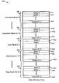
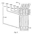
- FIG. 1illustrates the arrangement of the typical flash memory cells in the typical flash memory device.
- a flash memory array 100comprising typical flash memory cells functions as a nonvolatile mass memory component of the typical flash memory device.
- the flash memory array 100is divided into a plurality of data blocks 102 , . . . , 106 for storing data.
- the data blocks 102 , . . . , 106are conventionally labeled from zero to M ⁇ 1, where M is the total number of data blocks 102 . . . , 106 .
- Each data block 102, . . .
- each data block 102 , . . . , 106is uniquely assigned a virtual physical block address (VPBA), the VPBA representing the typical flash memory system's method of identifying and addressing the data blocks 102 , . . . , 106 inside the typical flash memory device.
- VPBAvirtual physical block address
- each data block 102 , . . . , 106is selectively programmable and erasable.
- each data block 102 , . . . , 106includes a plurality of sectors 112 , . . . , 136 . Within each data block 102 , . . . , 106 , the sectors 112 , . . .
- Nis the number of sectors within each data block 102 , . . . , 106 . Since the data blocks 102 , . . . , 106 comprise typical flash memory cells, the data blocks 102 , . . . , 106 are nonvolatile, i.e., the data stored in the data blocks 102 , . . . , 106 is retained even when power is cut off.
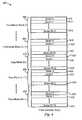
- FIG. 2illustrates the features of the sector 200 found in each data block.
- the sector 200includes a plurality of fields 202 , . . . , 212 .
- a DATA field 202is utilized for storing user data.
- the size of the DATA field 202is typically five hundred twelve bytes which corresponds with a storage sector length in a commercially available hard disk drive or floppy disk drive, the DATA field 202 can be configured to be practically any length of bytes.
- An extension field 204typically sixteen bytes, is seen to comprise an ECC field 206 for storing Error Correcting Code information associated with the DATA field 202 and is typically a length of four bytes.
- a virtual logical block address (VLBA) associated with the data stored in the DATA field 202is typically stored in a LOGICAL BLOCK ADDRESS field 208 of only one sector 200 in each block 102 , . . . , 106 . Rather than storing all the bits of the LBA associated with the data stored in the DATA field 202 of a particular sector 200 , only the higher order bits defining the VLBA are stored in the LOGICAL BLOCK ADDRESS field 208 . Data from each of the component LBA's which comprise the VLBA are stored in component sectors 112 , . . .
- An incoming LBA of User Datahas an address of higher order bits defining the general VLBA, and lower order bits defining the specific LBA.
- the processordefines the VLBA according to the higher order bits.
- the VLBAis then correlated to a specific VPBA of a Data Block 102 , . . . , 106 through the space manager 300 .
- component LBA's within a VLBAare then stored in component PBA's of the corresponding VPBA through a concatenation process.
- the lower order bits of an incoming LBAare concatenated onto the VPBA to form a PBA defining a particular sector 112 , . . . , 136 within a Data Block 102 , . . . , 106 .
- the logical block of incoming datais stored in that sector.
- a hostrequests retrieval of a specific LBA. Again, the lower order bits are masked, and the higher order bits define the more general VLBA.
- the VLBAis correlated to a VPBA through the space manager 300 .
- the Data Block 102 , . . . , 106 defined by the VPBAis located, the lower order bits of the requested LBA are concatenated on the VTBA to form a PBA defining the exact sector 1 12 , . . . , 136 where the data had been stored.
- the datais retrieved and sent to the host, defined according to the LBA by which the host requested it.
- the masking and concatenation process briefly described aboveinsures that the lower order bits of the logical address are the same as the lower order bits of the physical address, there is no need to store a correlation of the lower order bits. Accordingly, only the higher order bits comprising the VLBA are actually stored in the LOGICAL BLOCK ADDRESS field 208 of a physical sector 200 . As a result, the LOGICAL BLOCK ADDRESS field 208 is typically a length of two bytes. However, this length can be increased or decreased depending on the amount of addressable storage capacity supported by the typical flash memory system. Because all of the sectors 112 , . . . , 136 within a block 102 , . . .
- VLBAwithin their respective LOGICAL BLOCK ADDRESS, field 208 , typically, the VLBA is stored in the LOGICAL BLOCK ADDRESS field 208 of only one sector 112 , . . . , 136 per Data Block 102 , . . . , 106 .
- a FLAG field 210is employed for storing a plurality of flags pertaining to conditions of the data block of which the sector 200 is a part.
- the flags stored in the FLAG field 210include a defective block flag, an old/new block flag for indicating if stored data is obsolete, and a used/free block flag.
- the FLAG field 210is typically a length of one byte.
- the sector 200usually includes a plurality of SPARE bits 212 which are utilized when needed.
- the typical flash memory systemperforms a data storage algorithm purposely designed to overcome the limitations of flash memory technology while retaining compatibility with existing operating systems and existing application software.
- One technique for implementing the data storage algorithminvolves employing a space manager component to maintain a correlation between a virtual logical block addresses (VLBA) and a virtual physical block addresses (VPBA) of data stored in the typical flash memory system.
- VLBAvirtual logical block addresses
- VPBAvirtual physical block addresses
- the typical flash memory systemmust change the correlation between the LBA and the PBA because the updated versions of the data are programmed into empty memory locations—inevitably having PBAs that are different from the PBA originally assigned to the LBA—rather than being programmed over the old versions of the data in memory locations having the PBA originally assigned to the LBA.
- the space manager 300plays a critical role in coordinating LBA-to-PBA correlation in the typical flash memory system.
- a host digital systemto which the typical flash memory system is coupled and to which the typical flash memory system provides nonvolatile mass storage, maintains organization of the data sent to the typical flash memory system by generating the LBA and associating the LBA with the data.
- the LBAis a logical address where the host digital system believes the data is stored in the typical flash memory system.
- the typical flash memory systemtransforms the LBA into the PBA, where the PBA is a physical address of the data block and a specific sector wherein the data is actually stored.
- each data blockincludes a plurality of sectors.
- the VPBAsince the VPBA only refers to the data block rather than the actual sector storing the data within the data block, further reference must be made to the LBA to determine which sector within the data block stores the data. As noted, this involves the concatenation of a plurality of lower order bits of an LBA onto the lower end of the VPBA, thereby defining a PBA or physical address of the sector storing the data associated with the LBA. Each LBA within a VLBA is transformed into the physical address (the PBA) of one of the sectors.
- the typical flash memory systemsupports and recognizes a quantity of LBAs equal to the total number of sectors in the typical flash memory system.
- the bit length of the LBAs and the PBAsis directly related to the addressable storage capacity supported by the host digital system and the typical flash memory system.
- Maintaining the correlation between LBAs and PBAs of the data stored in the typical flash memory systemis critical to the proper operation of the typical flash memory system since the host digital system is generally not configured to track continually changing PBAs of the data stored in the typical flash memory system.
- the typical flash memory systemtransforms the LBA into the PBA upon initially receiving the data.
- the typical flash memory systemassigns an updated LBA to an entirely new PBA defining a sector 112 , . . . , 136 which is part of an entirely new Data Block 102 , . . . , 106 since it cannot program new data into an old PBA without first implementing an erase procedure.
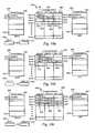
- the space manager 300is implemented as a volatile RAM array, the volatile RAM array including a plurality of volatile addressable memory locations 350 , . . . , 358 .
- Each volatile addressable memory location 350 , . . . , 358corresponds to one of the data blocks 102 , . . . , 106 (FIG. 1) in the typical flash memory system and stores information about the corresponding data block 102 , . . . , 106 (FIG. 1 ).
- FIG. 1illustrated the data blocks 102 , . . . , 106 conventionally labeled from zero to M ⁇ 1.
- the volatile addressable memory locations 350, .
- each volatile addressable memory location 350 , . . . , 358is addressable by at least one of the VLBAs 360 , . . . , 368 received from the host digital system and by one of the VPBAs 312 , . . . , 320 of the typical flash memory system.
- Each volatile addressable memory location 350 , . . . , 358includes a plurality of fields 310 , . . . , 340 .
- the space manager 300comprises static random access memory (SRAM) cells. However, other memory cells can be substituted for the SRAM cells.
- SRAMstatic random access memory
- the space manager 300serves two purposes. First, the correlation between the virtual logical block address (VLBA) and the virtual physical block address (VPBA) of the data stored in the typical flash memory system is tracked in the space manager 300 , giving the typical flash memory system rapid access to this crucial correlation information.
- a VPBA field 310stores the VPBA assigned to the VLBA associated with the data received from the host digital system, where the VPBA is the address of the data block 102 , . . . , 106 (FIG. 1) used to store data associated with a VLBA.
- the length of the VPBA field 310is directly related to the addressable storage capacity supported by the typical flash memory system. Typically, the VPBA field 310 is a length of two bytes.
- the typical flash memory systememploys the space manager 300 to keep track of the flags associated with the data blocks 102 , . . . , 106 (FIG. 1 ). Since each volatile addressable memory location 350 , . . . , 358 corresponds to one of the data blocks 102 , . . . , 106 (FIG. 1 ), the flags associated with the corresponding data block 102 , . . . , 106 (FIG. 1) are maintained in flag fields 320 , . . . , 340 within the volatile addressable memory location 350 , . . . , 358 .
- these flagsinclude the defective block flag 320 , the old/new or obsolete block flag 330 , and the used/free block flag 340 .
- Setting the defective block flag 320 of the data block 102 , . . . , 106 (FIG. 1)causes the flash memory system to avoid storing the data in any of the sectors in the data block 102 , . . . , 106 (FIG. 1) since the entire data block 102 , . . . , 106 (FIG. 1) is deemed defective.
- Setting the used/free block flag 340 of the data block 102 , . . . , 106 (FIG. 1)indicates the data block 102 , . . . , 106 (FIG.
- the typical flash memory systemutilizes the space manager 300 to search for the data block with an unset defective block flag 320 and an unset used/free block flag 340 for storing the data.
- the datais stored in the data block with the unset defective block flag 320 and the unset used/free block flag 340 .
- the VPBA of the data block with the unset defective block flag 320 and the unset used/free block flag 340is stored in the VPBA field 310 of the volatile addressable memory location 350 , . . . , 358 addressable by the VLBA 360 , . . . , 368 .
- the typical flash memory systemalso sets the used/free block flag 340 of the volatile addressable memory location 350 , . . . , 358 addressable by the VPBA 312 , . . . , 320 of the data block storing the data.
- the typical flash memory systemproceeds as described above, thus avoiding the erase-before-write cycle.
- the typical flash memory systemsets the old/new block flag 330 of the volatile addressable memory location 350 , . . . , 358 addressable by the current VPBA 312 , . . . , 320 to prevent the typical flash memory system from accessing unneeded versions of the data stored in the current PBA.
- the typical flash memory systememploys the space manager 300 in performing the read operation. After the host digital system provides the LBA associated with requested data, the typical flash memory system locates the PBA assigned to the LBA by reading the contents of the VPBA field 310 of the volatile addressable memory location 350 , . . . , 358 addressable by the LBA 360 , . . . , 368 . The typical flash memory system reads out the requested data from the data block whose PBA is assigned to the provided LBA.
- the space manager 300assists the typical flash memory system in executing the erase operation.
- the typical flash memory systemcan perform the erase operation in the background, i.e., while another operation is being performed, or when necessary.
- the typical flash memory systemuses the space manager 300 to search for the data blocks having a set old/new block flag 330 and an unset defective block flag 320 —these data blocks need to be erased. This search is conducted by examining the flag fields 320 and 330 (defective block and old/new or obsolete block) of the volatile addressable memory locations 350 , . . . , 358 .
- the typical flash memory systemerases the data blocks having the set old/new block flag 330 and the unset defective block flag 320 .
- each VLBA having an assigned VPBAis stored in the LOGICAL BLOCK ADDRESS field 208 (FIG. 2) of the data block corresponding to the assigned VPBA.
- a distinct advantage of this featurerests in the non-volatile nature of the flash memory. Since the data blocks are nonvolatile, loss of power has no effect on the memory contents of the data blocks. This provides a non-volatile correlation between logical and physical addresses in the event of power loss.
- the typical flash memory systemrestores the memory contents of the space manager 300 .
- the FLAG field 210 (FIG. 2) of each data blockis used to update the flag fields 320 , . . . , 340 of the corresponding volatile addressable memory location 350 , . . . , 358 .
- the controlleris able to load the VPBA of the particular data block 102 , . . . , 106 into an appropriate volatile addressable memory location 350 , . . . , 358 corresponding to the appropriate VLBA 360 , . . . , 368 .
- the typical flash memory systemfurther comprises a controller coupled to the typical flash memory device.
- the space manager 300is an integral part of the operations performed by the typical flash memory system, the space manager 300 is typically designed within the controller. This increases system performance.
- the controlleris formed on an integrated circuit separate from that on which the typical flash memory device is formed since the silicon area necessary for a large addressable storage capacity would generally make economically unfeasible formation of both the controller and the typical flash memory device on an identical integrated circuit. Additionally, formation of the controller on the separate integrated circuit allows the implementation of the controller in a manufacturing technology more suited for the performance demands placed on the controller by the typical flash memory system.
- the space manager 300enables the typical flash memory system to achieve superior performance, this superior performance, is attained at a significant cost in silicon area on the integrated circuit on which the controller is formed.
- the 64 MegaBit flash memory systemcomprises one 64 MegaBit flash memory device having 1024 data blocks, each data block including 16 sectors. This flash memory system supports 16,384 LBAs.
- the space manager 300 of the 64 MegaBit flash memory systemwill have 1024 volatile addressable memory locations 350 , . . . , 358 .
- the column containing the VPBA field 310(which is two bytes in length) will occupy:
- VPBA field 310a length of 10 bits for the VPBA field 310 would be sufficient to store unique physical block addresses for the 1024 data blocks, manipulating PBAs which are identified in byte lengths (8 bits or multiples of 8 bits) optimizes operation of the typical flash memory system. Additionally, the 16 bit length of the VPBA field 310 accommodates expansion of the addressable storage capacity supported by the controller.
- the size of the space manager 300 within the controllerincreases significantly as the typical flash memory system is configured to support a larger amount of addressable storage capacity, as demonstrated by the calculations below.
- this flash memory systemcomprises eight 64 MegaBit flash memory devices.
- the 128 MegaByte, 256 MegaByte, 512 MegaByte, and 1 GigaByte flash memory systemscomprise a plurality of flash memory devices configured to store an appropriate amount of data.
- the length of the VPBA field 310(FIG. 3) increased to 24 bits because 17 bits are required in order to store unique physical block addresses for the 131,072 data blocks and because a length of 3 bytes (24 bits) is the next available byte size.
- space managers 300FIG.
- controllers having space managers 300 (FIG. 3) of vastly different memory sizesare required in order for the typical flash memory system to economically support increasing amounts of addressable storage capacity. In essence, the utility of the controller is limited by the size of the space manager 300 (FIG. 3 ).
- the present inventionis a flash memory system designed to reduce inefficiencies associated with keeping track of logical block address (LBA) to physical block address (PBA) correlation as practiced in the prior art—each logical block address generated by a host digital system and associated with data when the data is sent to be stored in the flash memory system by the host digital system.
- the flash memory systempreferably comprises at least one flash memory device having a flash memory array, the flash memory array including a plurality of blocks for storing data and for storing a LBA-to-VPBA correlation, each block having a plurality of sectors, and a controller coupled to each flash memory device, the controller including a new space manager.
- each correlation blockis configured to store the physical block addresses corresponding to a predetermined range of logical block addresses.
- each correlation blockis associated with a predetermined range of logical block addresses although the physical block addresses are the addresses actually stored in each correlation block. Since the correlation blocks maintain their contents even when power is turned off, there is no need to maintain copies of the contents of the correlation blocks in other memory locations within the flash memory system.
- an erase-before-write cyclei.e., performing an erase operation immediately before performing a write operation
- new correlation informationi.e., the new LBA-to-VPBA relation
- a free sector of an appropriate correlation blocki.e., a correlation block associated with the predetermined range of logical block addresses which includes the LBA or LBAs affected by the new correlation information, rather than erasing and then programming a previously programmed sector of the appropriate correlation block.
- Each predetermined range of logical block addressesis associated with a current sector.
- Each current sectorstores current correlation information, i.e., current LBA-to-VPBA relations, relating to the logical block addresses within the associated predetermined range of logical block addresses.
- current correlation informationi.e., current LBA-to-VPBA relations
- the flash memory system of the present inventionalso simultaneously programs unchanged correlation information, i.e., unchanged LBA-to-VPBA relations, from the current sector into the free sector of the appropriate correlation block.
- Programming correlation information, i.e., LBA-to-VPBA relations, into the correlation blockis crucial to the proper operation of the flash memory system of the present invention.
- a first programming operationi.e., programming the data into an appropriate data block
- a second programming operationi.e. programming the correlation information of the data into the appropriate correlation block
- the flash memory system of the present inventionoptimizes system performance which would otherwise deteriorate because multiple programming operations are executed in the flash memory device, unlike the prior art where only the data has to be programmed into the typical flash memory device.
- programming the correlation information into the appropriate correlation blockis kept as much as possible in the background, i.e., performed while another operation is being performed, or relegated to periods of system inactivity, i.e., performed when no other operation is being performed.
- the flash memory system of the present inventionpreferably includes at least one alternate correlation block. Configured similarly to the correlation blocks, each alternate correlation block is associated with a primary correlation block and stores the physical block addresses corresponding to the predetermined range of logical block addresses associated with the primary correlation block.
- the flash memory system of the present inventioncan store in the free sector of the alternate correlation block the new correlation information and the unchanged correlation information from the current sector when the free sector is not found in the primary correlation block.
- the flash memory system of the present inventionavoids erasing the primary correlation block until a more convenient and, efficient time. Since the primary correlation block is erased before the alternate correlation block is completely filled, the primary correlation block is again available for storing the correlation information when the alternate correlation block is filled.
- the flash memory system of the present inventionincludes components for tracking each current sector and means for allocating a nondefective block to replace a defective correlation block. Having the components for tracking each current sector eliminates the need for performing read operations on the correlation block each time the flash memory system of the present invention accesses the correlation block in order to determine the free sector, thus improving system performance. Once a block is flagged as defective, the flash memory system of the present invention avoids accessing the defective block. Unlike the other blocks, correlation blocks are essential to the flash.memory system of the present invention. Hence, the nondefective block must be assigned to replace permanently the defective correlation block, a task accomplished by the means for allocating.
- the flash memory system of the present inventionincludes more than one flash memory device, system performance is enhanced by keeping track of the correlation between the LBAs and the PBAs of the data stored in a first flash memory device in the correlation block of a second flash memory device while keeping track of the correlation between the LBAs and the PBAs of the data stored in the second flash memory device in the correlation block of the first flash memory device.
- This techniquemaximizes system performance because the data and the correlation information can be programmed concurrently. Proceeding according to this technique enables the flash memory system of the present invention to program the correlation information relating to the data being stored in the first flash memory device into the correlation block of the second flash memory device while concurrently programming the data into the data block of the first flash memory device. Similarly, the flash memory system of the present invention can program the correlation information relating to the data being stored in the second flash memory device into the correlation block of the first flash memory device while concurrently programming the data into the data block of the second flash memory device.
- FIG. 1illustrates an organization of a flash memory array in a typical flash memory system according to the prior art.
- FIG. 2illustrates a configuration of a sector in a typical flash memory system according to the prior art.
- FIG. 3illustrates a configuration of a space manager in a typical flash memory system according to the prior art.
- FIG. 4illustrates an organization of a flash memory array in a flash memory system according to a first preferred embodiment of the present invention.
- FIG. 5illustrates a configuration of a sector of the correlation block in a flash memory system according to a first preferred embodiment of the present invention.
- FIG. 6illustrates a configuration of correlation blocks-in a flash memory system according to a first preferred embodiment of the present invention.
- FIG. 7illustrates the storage of incoming data in a new VPBA.
- FIG. 8illustrates a configuration of a sector of a data block in a flash memory system according to a first preferred embodiment of the present invention.
- FIG. 9illustrates a configuration of a new space manager in a flash memory system according to a first preferred embodiment of the present invention.
- FIGS. 10A through 10Cillustrate a sequence of operations performed, on a correlation block and on a volatile RAM array responsible for storing designations identifying current sectors, by a flash memory system according to a first preferred embodiment of the present invention.
- FIG. 11illustrates a configuration of a first flash memory device and a second flash memory device in a flash memory system according to a first preferred embodiment of the present invention.
- FIG. 12illustrates a configuration of a first flash memory device and a second flash memory device in a flash memory system according to a second preferred embodiment of the present invention.
- FIG. 13illustrates a configuration of correlation blocks in a 64 MegaBit flash memory system according to a first preferred embodiment of the present invention.
- FIG. 14illustrates a configuration of a volatile RAM array responsible for storing designations identifying current sectors in a 64 MegaBit flash memory system according to a first preferred embodiment of the present invention.
- the flash memory system of the present inventionincorporates a flash memory architecture which keeps track of logical block address (LBA) to physical block address (PBA) correlation within a nonvolatile mass memory component rather than in a volatile specialized memory component as practiced in the prior art.
- LBAlogical block address
- PBAphysical block address
- This implementationis stable, i.e., interruptions in power supplied to the flash memory system will not wipe out a current representation of the VLBA-to-VPBA correlation in the nonvolatile mass memory component, unlike the prior art where loss of power wipes out the current representation of the VLBA-to-VPBA correlation in the volatile specialized memory component thus necessitating the typical flash memory system of the prior art to undertake a series of operations to reconstruct the current representation of the VLBA-to-VPBA correlation in the volatile specialized memory component.
- the flash memory system of the present inventionexhibits qualities superior to the typical flash memory system of the prior art.
- the flash memory systemavoids the costs associated with dedicating increasing amounts of memory space to the volatile specialized memory component as addressable storage capacity supported by the flash memory system is expanded. Additionally, the flash memory system features a measure of flexibility in dealing with limitations of flash memory technology, such as the proneness of flash memory cells to wear-out and the necessity of performing an erase operation on the flash memory cells before reprogramming the flash memory cells. More particularly, a greater number of design options are available for the flash memory system, thus making possible cost effective specialized designs for the flash memory system for a variety of storage applications.
- the flash memory systemis coupled to a host digital system, such as a host computer system, and provides nonvolatile mass storage for use by the host digital system.
- a host digital systemsuch as a host computer system
- Data to be stored in or to be read from the flash memory systemis associated by the host digital system with one of a plurality of logical block addresses generated by the host digital system.
- the flash memory systemtransforms the logical block address into one of a plurality of physical block addresses—refer to the “Background of the Invention” for a discussion of the need for this transformation.
- the flash memory systemcomprises at least one flash memory device for storing the data and correlation information, i.e., LBA-to-VPBA relations, and a controller for controlling operations performed by the flash memory system.
- data and correlation informationi.e., LBA-to-VPBA relations
- Each flash memory devicecomprises a flash memory array, the flash memory array including a plurality of flash memory cells.
- the flash memory cellsare nonvolatile memory cells.
- the flash memory arrayrepresents the nonvolatile mass memory component described above.
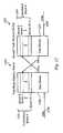
- FIG. 4for an illustration of an organization of the flash memory array 400 within the flash memory device of the flash memory system according to a first preferred embodiment of the present invention.
- the flash memory array 400 of the present inventionincludes a plurality of blocks 460 , . . . , 490 and a plurality of sectors 412 , . . . , 440 .
- the flash memory array 400preferably includes at least one data block 470 , . .
- each data block 470 , . . . , 490is configured to store the data received from the host digital system and is configured as described in the “Background of the Invention” and in FIGS. 1 and 2.
- each correlation block 460 , . . . , 465is in fact a block that is used to track VLBA-to-VPBA correlation.
- Each correlation block 460 , . . . , 465is configured to store the virtual physical block address (VPBA) assigned to the virtual logical block address (VLBA) received from the host digital system. Accordingly, each correlation block 460 , . . .
- each data block 470 , . . . , 490 and each correlation block 460 , . . . , 465is selectively programmable and erasable.
- the correlation blocks 460 , . . . , 465are labeled from zero to L ⁇ 1, where L is the total number of correlation blocks 460 , . . . , 465 in the flash memory device.
- the flash memory deviceis designed to have a sufficient number of correlation blocks 460 , . . . , 465 so that the VPBAs assigned to the VLBAs supported by the flash memory device can be stored in the flash memory device.
- the configuration of each data block 470 , . . . , 490determines the total number of LBAs supported by the flash memory device. However, the total number of LBAs supported by the flash memory system is obtained by summing the total number of LBAs supported by each flash memory device in the flash memory system.
- each correlation block 460 , . . . , 465reduces an equivalent amount of addressable storage capacity from the flash memory device in the flash memory system.
- the data blocks 470 , . . . , 490are labeled from L to M ⁇ 1, where M is the total number of blocks 460 , . . . , 490 existing in the flash memory device before select blocks 460 , . . . , 465 were converted into correlation blocks 460 , . . .
- each correlation block 460 , . . . , 465includes a plurality of sectors 412 , . . . , 422 .
- the sectors 412 , . . . , 422are labeled from zero to N ⁇ 1, where N is the number of sectors 412 , . . . , 422 within each correlation block 460 , . . . , 465 .
- each data block 470 , . . . , 490includes a plurality of sectors 424 , . . . , 440 .
- the sectors 424 , . . . , 440are labeled from zero to N ⁇ 1, where N is the number of sectors 424 , . . . , 440 within each data block 470 , . . . , 490 .
- the sectors 412 , . . . , 422 . in each correlation block 460 , . . . , 465are not configured similarly to the sectors 424 , . . . , 440 in each data block 470 , . . . , 490 , as will be described below.
- each sector 424 , . . . , 440 in each data block 470 , . . . , 490supports one LBA
- the total number of sectors 424 , . . . , 440 found in the data blocks 470 , . . . , 490determines the total number of LBAs supported by the flash memory device.
- FIG. 4is merely intended to illustrate a particular arrangement of the correlation blocks 460 , . . . , 465 , but is not meant to limit the arrangement of the correlation blocks 460 , . . . , 465 in the flash memory array 400 of the flash memory system to the particular arrangement disclosed.
- the correlation blocks 460 , . . . , 465can be distributed through out the flash memory array 400 rather than clustered together as shown in FIG. 4 .
- FIG. 5illustrates the features of the sector 500 as configured in each correlation block.
- the sector 500includes a plurality of fields 510 , . . . , 560 .
- a plurality of VPBA fields 510 , . . . , 540are utilized for storing the VPBA assigned to the VLBA received from the host digital system.
- These VPBA fields 510 , . . . , 540are functionally equivalent to the VPBA field 310 (FIG. 3) discussed in connection with the space manager 300 (FIG. 3) of the prior art.
- 540is configured in byte lengths (8 bits or multiples of 8 bits). Inasmuch as a VPBA field 510 , . . . , 540 must be large enough to store a Virtual Logical Block Address, the length of the VPBA is directly related to the addressable storage capacity supported by the flash memory system. Additionally, the total number of VPBA fields 510 , . . . , 540 included within each sector 500 is designed such that the total number of VPBA fields 510 , . . . , 540 occupies no more than an area 505 equivalent to the length of the DATA field 202 (FIG. 2) described in connection with the sector 200 (FIG. 2) of the prior art.
- the area 505is preferably a length of five hundred twelve bytes, but can be configured to other lengths.
- Each VPBA field 510 , . . . , 540is designated a predetermined VLBA representing a predetermined number of LBAs from the predetermined range of logical block addresses associated with the correlation block of which the sector 500 is a part.
- that VPBAis stored in the correlation block, specifically in the VPBA field 510 , . . . , 540 whose predetermined VLBA matches the received VLBA.
- the sector 500also includes an ECC field 550 .
- the ECC field 550is configured to store Error Correcting Code information associated with the area 505 containing the VPBA fields 510 , . . . , 540 .
- the ECC field 550is a length of four bytes, which is sufficient to handle the Error Correcting Code information generated by an Error Correcting Code algorithm implemented in the flash memory system of the present invention.
- other available Error Correcting Code algorithmscould possibly necessitate the ECC field 550 to be configured to a different length.
- the VPBA field 310 of the space manager 300lacks ECC protection. Accordingly, ECC protection for the VPBA fields 510 , . . . , 540 is a unique advantage of the present invention which is particularly well suited for applications requiring a greater level of fault-free performance.
- the sector 500includes a Flag field 570 containing a plurality of flags and a SPARE field 560 containing a plurality of spare bits which are utilized when needed.
- FIG. 6illustrates with greater detail the correlation blocks 660 , . . . , 675 of the flash memory array of the flash memory device in the flash memory system according to the first preferred embodiment of the present invention.
- the position of the data blocks 680 relative to the correlation blocks 660 , . . . , 675has been indicated but the discussion will focus and emphasize the configuration of the correlation blocks 660 , . . . , 675 .
- four correlation blocks 660 , . . . , 675were sufficient to keep track of the VLBA-to VPBA correlation for the flash memory system.
- Fields 610 , . . . , 630correspond to the VPBA fields 510 , . . . , 540 of FIG. 5 .
- ECC field 635corresponds to the ECC field 550 of FIG. 5 .
- SPARE field 640corresponds to the SPARE field 560 of FIG. 5 .
- Correlation Block 0 660 and on Correlation Block 1 665have the identical configuration, thus they are associated with the same predetermined range of logical block addresses (i.e., VLBA 0 to VLBA Y ⁇ 1).
- the flash memory systemis configured such that Correlation Block 0 660 and Correlation Block 1 665 are interdependent, i.e., physical block addresses are stored in either Correlation Block 0 660 or Correlation Block 1 665 depending on which correlation block has a free sector, i.e., a sector which has not been programmed or has been both programmed and erased, thus avoiding the erase-before-write cycle.
- Correlation Block 2 670 and Correlation Block 3 675have the identical configuration, thus they are configured with the same predetermined range of logical block addresses (i.e., VLBA Y to VLBA Z ⁇ 1).
- the flash memory systemis also configured such that Correlation Block 2 670 and Correlation Block 3 675 are interdependent, i.e., physical block addresses are stored in either Correlation Block 2 670 or Correlation Block 3 675 depending on which correlation block has the free sector, i.e., the sector which has not been programmed or has been both programmed and erased.
- each primary correlation block 660 & 670is preferably associated with at least one alternate correlation block 665 & 675 . Eliminating the alternate correlation blocks 665 & 675 from the flash memory system increases the addressable storage capacity supported by the flash memory system.
- the present inventionintroduces design options for the flash memory system and allows compromises to be made within these design options in order to optimize the configuration of the flash memory system for any application under consideration.
- Sector 0 642 of Correlation Block 0 660illustrates the predetermined VLBAs, as described above, assigned to each VPBA field 610 , . . . , 630 .
- the predetermined VLBAsare not actually stored in each VPBA field 610 , . . . , 630 .
- the predetermined range of logical block addresses associated with Correlation Block 0 660extends from VLBA 0 to VLBA Y ⁇ 1, where Y is the number of VLBAs assigned to the VPBA fields 610 , . . . , 630 of Correlation Block 0 660 .
- each data block 470 , . . . , 490includes N sectors—each sector supporting one LBA—, each VPBA will support N logical block addresses (LBAs), hence N predetermined LBAs are assigned to each VPBA field 610 , . . . , 630 of Correlation Block 0 660 .
- LBAslogical block addresses
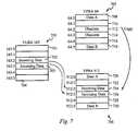
- VLBA 163 700is comprised of only six LBA's 701 , . . . , 704 , and VPBA 64 705 and VPBA 912 706 are respectively only six sectors 708 , . . . , 718 & 720 , . . . , 730 in size.
- the number of LBA's per VLBAis equal to the number of sectors (PBA's ) per VPBA, as illustrated.
- each VPBAwould be comprised of PBA's which, in number, were a power of two. More preferably, each VPBA would be comprised of sixteen or thirty two PBA's. Accordingly, the preferred embodiment would not typically disclose a VPBA comprised of six PBA's which is used for ease of illustration.
- two LBA's 702 , 703 of incoming databoth comprising the same VLBA 700 defined by VLBA 163 are received by the flash memory system.
- the previous data block 705 used to store VLBA 163was defined as VPBA 64 . It is noted that the first and last sector 708 , 718 of that data block 705 store data, as well as the middle two sectors 712 , 714 which are being rendered obsolete as a result of the incoming data in LBA's 702 , 703 .
- incoming datamay comprise any number of LBA's, from one, to all of the LBA's defining a VLBA.
- the VPBA of the new data block 706is stored in the current sector 642 , . . . , 656 (FIG. 6) of the VPBA field 610 , . . . , 630 which is correlated to the LBA that defined the incoming data.
- the fields of FIG. 6are displayed in terms of LBA's rather than VLBA's. For example, in sector zero 642 of the first column 610 of VPBA fields, the VPBA field is seen as correlated to LBA 0 through N ⁇ 1.
- a VLBAis comprised of N LBA's.
- each VPBA fieldcould equally be depicted as being correlated to a single VLBA rather than a range of N LBA's, zero through N ⁇ 1.
- each VPBA field 610 , . . . , 630is conveniently illustrated as correlating to a range of N LBA's rather than a single VLBA.
- the correlation relationships hereinare variously referred to as an LBA-to-VPBA correlation, and a VLBA-to-VPBA correlation. Both are in fact true.
- incoming data being correlated to a VPBAis defined by an LBA or series of LBA's, but the range of LBA's correlated to each VPBA field VPBA is equivalent to a VLBA.
- the predetermined LBAsare incrementally assigned to the VPBA fields 610 , . . . , 630 in ascending order starting with VPBA field 610 .
- the assignment of the predetermined LBAscan be implemented in other formats apparent to those skilled in the art.
- Sector 0 650 of Correlation Block 2 670illustrates additional predetermined LBAs assigned to each VPBA field 610 , . . . , 630 .
- the predetermined range of logical block addresses associated with Correlation Block 2 670extends from LBA Y to LBA Z ⁇ 1.
- each correlation block 660Preferably, within each correlation block 660 , . . .
- Sector 1 [ 643 , 647 , 651 , and 655 ] through Sector(N ⁇ 1) [ 644 , 648 , 652 , and 656 ]are configured similarly to Sector 0 [ 642 , 646 , 650 , and 654 ].
- FIG. 6is merely intended to illustrate a particular configuration of the correlation blocks 660 , . . . , 675 but is not meant to limit the configuration of the correlation blocks 660 , . . . , 675 in the flash memory system to the particular configuration disclosed. Other configurations are possible.
- the LBAsare uniquely assigned to the VPBA fields 510 , . . . , 540 (FIG. 5) in the correlation block 660 , . . . , 675 (FIG. 6 ), it is unnecessary to store the LBAs in the LOGICAL BLOCK ADDRESS field 208 (FIG. 2) in the data blocks 470 , . . . , 490 (FIG. 4 ), as is done in the prior art. As discussed in the “Background of the Invention”, the space manager 300 (FIG. 3) of the prior art loses its contents when power is turned off, hence the LOGICAL BLOCK ADDRESS field 208 (FIG.
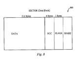
- FIG. 8illustrates an alternative configuration for the sectors 424 , . . . , 440 (FIG. 4) in the data blocks 470 , . . . , 490 (FIG. 4 ).
- the configuration in FIG. 8is similar except for not having the LOGICAL BLOCK ADDRESS field 208 (FIG. 2 ). This configuration conserves memory space in the flash memory system of the present invention.
- the flash memory systempreferably includes a controller coupled to each flash memory device.
- the controllerincludes logic circuitry to control and to manage the read operation, the write operation, and the erase operation. Additionally, the controller is configured to control the configuration of the data blocks 470 , . . . , 490 (FIG. 4) and the configuration of the correlation blocks 460 , . . . , 465 (FIG. 4 ). In particular, the controller can adjust the length of each VPBA field 510 , . . . , 540 (FIG. 5) and can configure the necessary correlation blocks 460 , . . . , 465 (FIG.
- the controlleris configured to write and to read the correlation information in correlation blocks 460 , . . . , 465 (FIG. 4) and is configured to write and to read the data received from the host digital system in the data blocks 470 , . . . , 490 (FIG. 4 ).
- the controllerincludes a new space manager.
- FIG. 9illustrates the configuration of the new space manager 900 .
- the new space manager 900keeps track of the flags associated with the data blocks 470 , . . . , 490 (FIG. 4) and the correlation blocks 460 , . . . , 465 (FIG. 4) in the manner discussed in the “Background of the Invention”.
- the new space manager 900represents the volatile specialized memory component described above.
- the new space manager 900preferably comprises a new volatile RAM array, the new volatile RAM array preferably including SRAM memory cells.
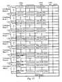
- the new space manager 900includes a plurality of volatile addressable memory locations 940 , . . . , 948 .
- Each volatile addressable memory location 940 , . . . , 948corresponds to one of the blocks 460 , . . . , 490 (FIG. 4 ), including both data blocks 470 , . . . , 490 and correlation blocks 460 , . . . , 465 (FIG. 4 ).
- Status information concerning each of these blocks 460 , . . . , 490is stored in the space manager 900 .
- the new space manager 900will include m ⁇ 1 volatile addressable memory locations 940 , . . . , 948 , preferably equal to the number of VPBAs 950 , .
- each volatile addressable memory location 940 , . . . , 948includes a plurality of fields 910 , . . . , 930 . These fields include the defective block flag 910 , the old/new (obsolete) block flag 920 , and the used/free block flag 930 , as identified in the “Background of the Invention”. Since the new space manager 900 does not include the VPBA field 310 (FIG. 3) as in the space manager 300 (FIG. 3) of the prior art, there is a marked reduction in logic circuitry space requirement for the new space manager 900 in the controller when compared to the logic circuitry space requirement for the space manager 300 (FIG. 3) of the prior art.
- each correlation block 660 , . . . , 675includes sectors 642 , . . . , 656 which are configured to store the VPBAs assigned to the LBAs within the predetermined range of logical block addresses associated with each correlation block 660 , . . . , 675 .
- the flash memory systemincludes components to facilitate the tracking of the ( VLBA-to PBA) correlation within each correlation block 660 , . . . , 675 . Rather than reading each sector 642 , . . . , 656 in each correlation block 660 , . . . , 675 to determine a current sector before writing the correlation information in each correlation block 660 , .
- the controllerpreferably includes means for storing a designation identifying the current sector for each predetermined range of logical block addresses, means for generating the designation, and means for decoding the designation.
- Each current sectorstores current correlation information, i.e., current VLBA-to-VPBA relations for a predetermined range of logical block addresses.
- each predetermined range of logical block addressesis associated with one current sector. Since each designation uniquely identifies the current sector for each predetermined range of logical block addresses, the number of correlation blocks 660 , . . . , 675 associated with each predetermined range of logical block addresses as well as the number of sectors 642 , . . . , 656 in each correlation block 660 , . .
- . , 675determine the length of the designation. As an example, assuming two correlation blocks are associated with a predetermined range of logical block addresses and each correlation block has sixteen sectors, the designation would have to be capable of uniquely identifying thirty-two sectors because any one of the thirty-two sectors could be the current sector. For this example, a length of one byte would be sufficient to enable the designation to uniquely identify any one of the thirty-two sectors.
- the designationcan be implemented as any appropriate implementation known to those skilled in the art.
- the means for storing the designationis preferably implemented as a volatile RAM array or an equivalent discussed in greater detail in conjunction with element 1004 (FIGS. 10 a - 10 c ).
- the volatile RAM. arraycomprises SRAM memory cells.
- the volatile RAM arraycan comprise other types of RAM memory cells known to those skilled in the art.
- the volatile RAM arrayincludes a plurality of addressable volatile memory locations. Each addressable volatile memory location corresponds with one of the predetermined ranges of logical block addresses associated with the correlation blocks 660 , . . . , 675 . Each addressable volatile memory location stores the designation identifying the current sector associated with the predetermined range of logical block addresses corresponding with the addressable volatile memory location.
- the volatile RAM arrayincludes a sufficient number of volatile memory locations to enable the controller to function in a wide range of memory configurations for the flash memory system.
- the logic circuitry space occupied by the volatile RAM array in the controlleris substantially less than the logic circuitry space occupied by the VPBA field 310 (FIG. 3) of the space manager 300 (FIG. 3) of the prior art because the volatile RAM array contains addressable volatile memory locations that are fewer in number and smaller in length than the VPBA field 310 (FIG. 3) of the space manager 300 (FIG. 3) of the prior art.
- the flash memory systemrestores the contents of the volatile RAM array by reading each sector 642 , . . . , 656 in each correlation block 660 , . . . , 675 to determine the current sector associated with each predetermined range of logical block addresses and then generating each designation to be stored in the volatile RAM array.
- the means for generating the designationgenerates the designation to be stored in the volatile RAM array.
- the means for decoding the designationdecodes the designation stored in the volatile RAM array.
- the flash memory systemuses the decoded designation to choose an appropriate sector in which to store correlation information relating to the LBA received from the host digital system.
- a block having a set defective block flagis not utilized by the typical flash memory system.
- the flash memory system of the present inventiondoes not utilize a data block or a correlation block having a set defective block flag.
- the controllerwhen a correlation block becomes defective, the controller will reconfigure and reassign an unused and non-defective data block to take the place of the defective correlation block.
- the process of keeping track of the VLBA-to-VPBA correlation in the correlation blocksis dependent on the configuration chosen for the flash memory system, i.e., the number of alternate correlation blocks associated with each primary correlation block. This design choice determines the system performance.
- the flash memory systemreceives data defined according to an LBA from the host digital system.
- the flash memory systemselects an appropriate data block in which to store the received data.
- the specific sector for storing a VLBA of incoming user datais designated by concatenating the lower order bits of the VLBA onto the VPBA, thereby defining the PBA of the sector designated for storage.
- the VPBA of the appropriate data blockis correlated with the received LBA by storing the VPBA in an appropriate correlation block associated with the predetermined range of logical block addresses encompassing the received LBA, unlike the prior art where the VPBA of the appropriate data block is stored in an appropriate volatile addressable memory location in the space manager 300 (FIG. 3 ). Within the appropriate correlation block, the VPBA is stored in the VPBA field whose predetermined LBA matches the received LBA.
- the flash memory systemdecodes, from the volatile RAM array, the designation identifying the current sector associated with the predetermined range of logical block addresses encompassing the received LBA.
- the flash memory systemutilizes this current sector information to determine and to locate the free sector, i.e., the sector which has not been programmed or has been both programmed and erased, in the appropriate correlation block.
- the flash memory systemfills in sequential order the sectors within the appropriate correlation block. As illustrated in conjunction with FIGS.
- the flash memory systemprograms the unchanged correlation information, i.e., LBA to PBA relations unaffected by the received LBA, from the current sector into the free sector simultaneously with programming the new VPBA into the free sector, thus the flash memory system avoids the erase-before-write operation which would be required if the flash memory system programmed the new correlation information, into the current sector. Finally, the flash memory system generates an updated designation identifying the current sector and stores the updated designation in an appropriate location in the volatile RAM array.
- the unchanged correlation informationi.e., LBA to PBA relations unaffected by the received LBA
- This process of tracking the LBA to VPBA correlationallows the flash memory system to store the data defined according to a plurality of LBAs in several data blocks and to update rapidly the correlation information relating to the LBAs in the correlations blocks after programming all the data in the data blocks, rather than updating the correlation information relating to each LBA after the data associated with each LBA is stored in the data blocks, thus increasing system performance.
- the flash memory system of the present inventionmust write to the flash memory device at least twice in order to complete the write operation since the flash memory system must program the data in the data blocks and program the correlation information in the correlation blocks.
- the flash memory systempreferably maintains system performance by programming the correlation information into the correlation blocks in the background, i.e., while performing another operation, or during periods of system inactivity, i.e., when no other operation is being performed, as much as possible. For example, after the flash memory system has programmed the data into the flash memory device and while communicating to the host digital system that the flash memory system is ready to process additional data, the flash memory system can program the correlation information into the correlation blocks in the flash memory device.
- the flash memory system of the present inventionis able to retrieve user data by means of the information within the correlation blocks which relate LBA's or VLBA's to a VPBA where the data is stored.
- the Flash Memory. Systemaccesses the data block of the designated VPBA and retrieves the requested data. When the requested data is sent to the host, it is defined according to the LBA or LBA's which had been requested by the host.
- a correlation blockis filled when there is no free sector available. If the correlation block does not have an alternate correlation block, the flash memory system must perform the erase-before-write operation on the filled correlation block. This procedure will increase the wearing-out rate of the filled correlation block and degrade system performance.
- the flash memory systemwill begin writing correlation data in an alternate correlation block, preferably beginning with the first sector. While filling the alternate correlation block, the flash memory system will erase the filled correlation block so that an erased correlation block is available when the alternate correlation block is filled. Similarly, a filled alternate correlation block will be erased before the correlation block is filled. This procedure avoids performing the erase-before-write operation, thus improving system performance.
- the flash memory systemproceeds as described above. However, since more than one alternate correlation block exists, the flash memory system is able to distribute the usage of the correlation block and alternate correlation blocks so as to minimize wearing-out of any one of the alternate correlation blocks and the correlation block. For example, once a first alternate correlation block is filled, the flash memory system can proceed to fill a second alternate correlation block rather than erasing the filled correlation block. There are many variations to this algorithm. All of these variations are part of the present invention. In addition, performing erase operations on the correlation block-and on each alternate correlation block is less frequently needed, conserving system resources and improving system performance.
- the flash memory systememploys the new space manager 900 (FIG. 9) including a flag field with flags indicating if a block is defective 910 , old (obsolete) 920 or used 930 . These flags 910 , 920 , 930 are useful in directing the controller in the performance of the erase operation. If a block is flagged as “old” (obsolete data), but not flagged as defective, it is targeted for erasure. As noted, the erase operation is preferably conducted as a “background” process so as not to interrupt or slow user operation.
- Sector 0 1016 of Correlation Block 0 1000stores the physical address VPBA 6 in a VPBA field 1040 correlated to a predetermined LBA range (LBA 0 through LBA 7 ) 1001 , indicating that data correlated to at least one LBA address in that predetermined range 1001 is currently stored in VPBA 6 .
- a volatile RAM array 1004is comprised of a variety of registers 1005 , 1006 . Each register 1005 , 1006 is dedicated to a different predetermined range of LBA's.
- the first register 1005is assigned to LBA range (LBA 0 -LBA 23 ), which is currently being tracked by Correlation Block 0 1000 .
- LBA rangeLBA 0 -LBA 23
- the range of twenty-four LBA's tracked per Correlation Blockis exemplary, and not intended to limit the present invention to any particular range.
- a correlation sector 500(FIG. 5) would comprise five hundred twelve usable bytes 505 , each VPBA field comprising two bytes, resulting in two hundred fifty-six VPBA fields 1040 , . . . , 1062 per sector 1016 , . . . , 1019 (FIGS. 10 a - 10 c ).
- incoming data 1020 defined as LBA 9is stored in VPBA 28 1022 .
- the first register 1005 of the volatile RAM array 1004indicates that the current sector for storing correlation data relating to LBA range zero through 23 was Correlation Block 0 1000 , Sector 0 1016 . If data retrieval were the issue, the controller would access the current sector 1016 . However, for the process of data storage and the concomitant storage of correlation data, the controller increments to the next sector, which is sector one 1017 .
- the incoming data 1020was defined as LBA 9 , it falls in the predetermined range (LBA, 8 to LBA 15 ) 1002 . Accordingly, the physical address “VPBA 28” of the newly received data is stored in the appropriate VPBA field 1048 of the new sector 1017 . All correlation data from the previous sector 1016 also remains valid unless overwritten. Accordingly, the address “VPBA 6” recorded in the first VPBA field 1040 of Sector 0 1016 is written in the same respective VPBA field 1046 of the new sector 1017 . Finally, the first field 1005 of the volatile RAM array 1004 , which identifies the current sector for correlation data to LBA range (LBA 0 through LBA 23 ), is updated, indicating that correlation data is now located in correlation block 0, Sector 1.
- the same basic processis seen to repeat itself in FIG. 10B, when incoming data 1024 defined by LBA 22 is stored in VPBA 23 1026 .
- the first register 1005 of the volatile RAM array 1004indicates “Block 0, Sector 1” prior to the storage of incoming data.
- the controllerincrements to the next sector 1018 .
- correlation datais stored in the appropriate VPBA field.
- LBA 22which defined the incoming data 1024 , falls in the predetermined range of (LBA 16 -LBA 23 ) 1003 .
- the new physical address VPBA 23is stored in a VPBA field 1052 corresponding to the predetermined LBA range 1003 in the new sector 1018 .
- current correlation data from the previous sector 1017 stored in VPBA fields 1046 , 1048 which are not being updatedare copied into corresponding VPBA fields 1052 , 1054 of the new sector 1018 .
- the corresponding register 1005 of the volatile RAM array 1004is seen to have been updated following the storage of correlation data in the new sector.
- the processis again repeated in FIG. 10C, when incoming data 1028 defined by LBA 2 is stored in VPBA 10 1030 .
- the first register 1005 of the volatile RAM array 1004indicates “Block 0, Sector 2” prior to the storage of incoming data.
- the controllerincrements to the next sector 1019 .
- correlation datais stored in the appropriate VPBA field.
- LBA 2which defined the incoming data 1028 , falls in the predetermined range of (LBA 0 -LBA 7 ) 1001 .
- the new physical address VPBA 10is stored in a VPBA field 1058 corresponding to the predetermined LBA range 1001 in the new sector 1019 .
- current correlation data from the previous sector 1018 stored in VPBA fields 1054 , 1056 which are not being updatedare copied into corresponding VPBA fields 1060 , 1062 of the new sector 1019 .
- the corresponding register 1005 of the volatile RAM array 1004is seen to have been updated following the storage of correlation data in the new sector.
- FIG. 11illustrates a configuration of a first flash memory device 1150 and a second flash memory device 1160 in a flash memory system according to a first preferred embodiment of the present invention.
- the flash memory systemprograms the correlation information PBA 1 relating to the data 1153 into the correlation block 1151 of the first flash memory device 1150 and programing the data 1153 into the data blocks 1152 of the first flash memory device 1150 .
- the flash memory systemprograms the correlation information PBA 2 relating to the data 1163 into the correlation block 1161 of the second flash memory system 1160 and programs the data 1163 , into the data blocks 1162 of the second flash memory system.
- system performanceis enhanced by keeping track of the correlation between the LBAs and the PBAs of the data 1153 stored in the first flash memory device 1150 in the correlation block 1161 of the second flash memory device 1160 while keeping track of the correlation between the LBAs and the PBAs of the data 1163 stored in the second flash memory device 1160 in the correlation block 1151 of the first flash memory device 1150 .
- This techniquemaximizes system performance because the data and the correlation information can be programmed concurrently.
- FIG. 12illustrates a configuration of a first flash memory device 1200 and a second flash memory device 1201 in a flash memory system according to a second preferred embodiment of the present invention
- the physical block address (PBA 2 ) of that data blockis stored in a proper correlation block 1202 of the first flash memory device 1200 .
- the “proper” correlation blockwill include within its range of VLB's the VLB of the incoming data 1205 .
- This techniquecan be expanded to flash memory systems having three or more flash memory devices. Essentially, the correlation information relating to the data stored in a particular flash memory device is not stored in the particular flash memory device. Instead, the correlation information relating to the data stored in the particular flash memory device is stored in a different flash memory device. This technique is applied to each flash memory device within the flash memory system having three or more flash memory devices.
- FIG. 13illustrates an example of a configuration of correlation blocks in a 64 MegaBit flash memory system according to a first preferred embodiment of the present invention.
- the 64 MegaBit flash memory systemcomprises one 64 MegaBit flash memory device having 1024 blocks, each block including 16 sectors, and a controller coupled to the 64 MegaBit flash memory device.
- the 64 MegaBit flash memory systemsupports slightly fewer than the 16,384 LBAs supported by the 8 correlation blocks because 8 blocks are configured as correlation blocks rather than data blocks, thus reducing the addressable storage capacity supported by the 64 MegaBit flash memory system, as explained above.
- each primary correlation block [ 1302 , 1304 , 1306 , and 1308 ]is associated with one alternate correlation block [ 1322 , 1324 , 1326 , and 1328 ].
- FIG. 14illustrates a volatile RAM array 1400 of the 64 MegaBit flash memory system shown in FIG. 13 .
- Each addressable volatile memory location 1410 , . . . , 1413has a corresponding predetermined range of logical block addresses 1401 , . . . 1404 .
- Each addressable volatile memory location 1410 , . . . , 1413stores the designation identifying the current sector associated with the corresponding predetermined range of logical block addresses 1401 , . . . , 1404 .
- LBA Wrepresents the largest LBA supported by the controller of the 64 MegaBit flash memory system. To enhance understanding of the present invention, the information represented by the designations is shown rather than the actual implementation of the designations. It should be understood by those skilled in the art that a binary implementation of the designation will be used to practice the present invention.
Landscapes
- Engineering & Computer Science (AREA)
- Theoretical Computer Science (AREA)
- Physics & Mathematics (AREA)
- General Engineering & Computer Science (AREA)
- General Physics & Mathematics (AREA)
- Techniques For Improving Reliability Of Storages (AREA)
- Read Only Memory (AREA)
Abstract
Description
| (Number of data blocks) | * | (Bit size of the VPBA field) = | |
| (1024) | * | (16 bits) = | 16,384 |
| bits | |||
| TABLE 1 |
| Relation between memory size of the flash memory system and the |
| memory size of the VPBA column in the space manager. |
| Size of flash | [ (Number of data blocks) * | Size of |
| memory system | (Bit size of VPBA field) ] | |
| 64 MegaByte: | [ (8192) * (16 bits) ] | = | 131,072 bits |
| 128 MegaByte: | [ (16,384) * (16 bits) ] | = | 262,144 bits |
| 256 MegaByte: | [ (32,768) * (16 bits) ] | = | 524,288 |
| 512 MegaByte: | [ (65,536) * (16 bits) ] | = | 1,048,576 |
| 1 GigaByte: | [ (131,072) * (24 bits) ] | = | 3,145,728 bits |
Claims (21)
Priority Applications (1)
| Application Number | Priority Date | Filing Date | Title |
|---|---|---|---|
| US09/660,838US6772274B1 (en) | 2000-09-13 | 2000-09-13 | Flash memory system and method implementing LBA to PBA correlation within flash memory array |
Applications Claiming Priority (1)
| Application Number | Priority Date | Filing Date | Title |
|---|---|---|---|
| US09/660,838US6772274B1 (en) | 2000-09-13 | 2000-09-13 | Flash memory system and method implementing LBA to PBA correlation within flash memory array |
Publications (1)
| Publication Number | Publication Date |
|---|---|
| US6772274B1true US6772274B1 (en) | 2004-08-03 |
Family
ID=32772342
Family Applications (1)
| Application Number | Title | Priority Date | Filing Date |
|---|---|---|---|
| US09/660,838Expired - LifetimeUS6772274B1 (en) | 2000-09-13 | 2000-09-13 | Flash memory system and method implementing LBA to PBA correlation within flash memory array |
Country Status (1)
| Country | Link |
|---|---|
| US (1) | US6772274B1 (en) |
Cited By (170)
| Publication number | Priority date | Publication date | Assignee | Title |
|---|---|---|---|---|
| US20020112101A1 (en)* | 1998-03-02 | 2002-08-15 | Petro Estakhri | Flash memory card with enhanced operating mode detection and user-friendly interfacing system |
| US20020136068A1 (en)* | 2000-12-20 | 2002-09-26 | Widdershoven Franciscus Petrus | Data processing device with a WOM memory |
| US20020188814A1 (en)* | 2001-06-08 | 2002-12-12 | Kenji Saito | Non-volatile storage device and rewrite control method thereof |
| US20030041210A1 (en)* | 2001-08-24 | 2003-02-27 | Micron Technology, Inc. | Erase block management |
| US20030126481A1 (en)* | 2001-09-28 | 2003-07-03 | Payne Robert Edwin | Power management system |
| US20030161199A1 (en)* | 2002-02-22 | 2003-08-28 | Petro Estakhri | Removable memory media with integral indicator light |
| US20040001370A1 (en)* | 2002-06-28 | 2004-01-01 | Fujitsu Limited | Nonvolatile semiconductor memory having partial data rewriting function |
| US20040199714A1 (en)* | 1995-07-31 | 2004-10-07 | Petro Estakhri | Increasing the memory performance of flash memory devices by writing sectors simultaneously to multiple flash memory devices |
| US20040237010A1 (en)* | 1992-05-20 | 2004-11-25 | Auclair Daniel L. | Soft errors handling in EEPROM devices |
| US6895490B1 (en) | 2001-04-09 | 2005-05-17 | Matrix Semiconductor, Inc. | Method for making a write-once memory device read compatible with a write-many file system |
| US20050120266A1 (en)* | 2002-02-06 | 2005-06-02 | Raul-Adrian Cernea | Memory device with sector pointer structure |
| US20050138050A1 (en)* | 2003-12-17 | 2005-06-23 | International Business Machines Corporation | System and method for estimating storage requirements for a multi-dimensional clustering data configuration |
| US20050162947A1 (en)* | 2004-01-27 | 2005-07-28 | Samsung Electronics Co., Ltd. | Data management apparatus and method of flash memory |
| US20050169058A1 (en)* | 2004-02-03 | 2005-08-04 | Samsung Electronics Co., Ltd. | Data management apparatus and method used for flash memory |
| US6996660B1 (en) | 2001-04-09 | 2006-02-07 | Matrix Semiconductor, Inc. | Memory device and method for storing and reading data in a write-once memory array |
| US7003619B1 (en) | 2001-04-09 | 2006-02-21 | Matrix Semiconductor, Inc. | Memory device and method for storing and reading a file system structure in a write-once memory array |
| US20060039196A1 (en)* | 2003-10-03 | 2006-02-23 | Gorobets Sergey A | Corrected data storage and handling methods |
| US7012835B2 (en) | 2003-10-03 | 2006-03-14 | Sandisk Corporation | Flash memory data correction and scrub techniques |
| US7051251B2 (en) | 2002-12-20 | 2006-05-23 | Matrix Semiconductor, Inc. | Method for storing data in a write-once memory array using a write-many file system |
| US7062602B1 (en) | 2001-04-09 | 2006-06-13 | Matrix Semiconductor, Inc. | Method for reading data in a write-once memory device using a write-many file system |
| US20060155922A1 (en)* | 2004-12-16 | 2006-07-13 | Gorobets Sergey A | Non-volatile memory and method with improved indexing for scratch pad and update blocks |
| US20060155921A1 (en)* | 2004-12-16 | 2006-07-13 | Gorobets Sergey A | Non-volatile memory and method with multi-stream update tracking |
| US20060155920A1 (en)* | 2004-12-16 | 2006-07-13 | Smith Peter J | Non-volatile memory and method with multi-stream updating |
| US20060161722A1 (en)* | 2004-12-16 | 2006-07-20 | Bennett Alan D | Scratch pad block |
| US7102671B1 (en) | 2000-02-08 | 2006-09-05 | Lexar Media, Inc. | Enhanced compact flash memory card |
| US20060245249A1 (en)* | 2005-04-27 | 2006-11-02 | Hwang Sang W | Nonvolatile memory devices that support virtual page storage using odd-state memory cells and methods of programming same |
| US7155559B1 (en)* | 2000-08-25 | 2006-12-26 | Lexar Media, Inc. | Flash memory architecture with separate storage of overhead and user data |
| US7167944B1 (en) | 2000-07-21 | 2007-01-23 | Lexar Media, Inc. | Block management for mass storage |
| US7185208B2 (en) | 2001-09-28 | 2007-02-27 | Lexar Media, Inc. | Data processing |
| US7188228B1 (en)* | 2003-10-01 | 2007-03-06 | Sandisk Corporation | Hybrid mapping implementation within a non-volatile memory system |
| US20070061545A1 (en)* | 2003-10-24 | 2007-03-15 | Hyperstone Ag | Method for writing memory sectors in a memory deletable by blocks |
| US20070083697A1 (en)* | 2005-10-07 | 2007-04-12 | Microsoft Corporation | Flash memory management |
| US20070136555A1 (en)* | 2005-12-13 | 2007-06-14 | Sinclair Alan W | Logically-addressed file storage methods |
| US7254668B1 (en) | 2002-10-28 | 2007-08-07 | Sandisk Corporation | Method and apparatus for grouping pages within a block |
| US20070208908A1 (en)* | 2004-08-24 | 2007-09-06 | Moore Christopher S | Method and apparatus for using a one-time or few-time programmable memory with a host device designed for erasable/rewriteable memory |
| US20080034259A1 (en)* | 2006-07-12 | 2008-02-07 | Gwon Hee Ko | Data recorder |
| US7340581B2 (en) | 2001-09-28 | 2008-03-04 | Lexar Media, Inc. | Method of writing data to non-volatile memory |
| US20080077842A1 (en)* | 2006-09-27 | 2008-03-27 | Gonzalez Carlos J | Memory with Cell Population Distribution Assisted Read Margining |
| US20080077841A1 (en)* | 2006-09-27 | 2008-03-27 | Gonzalez Carlos J | Methods of Cell Population Distribution Assisted Read Margining |
| US7359934B1 (en)* | 1999-02-04 | 2008-04-15 | Novell, Inc. | Multiple storage class distributed nametags for locating items in a distributed computing system |
| US7395404B2 (en) | 2004-12-16 | 2008-07-01 | Sandisk Corporation | Cluster auto-alignment for storing addressable data packets in a non-volatile memory array |
| US20080215802A1 (en)* | 2000-01-06 | 2008-09-04 | Super Talent Electronics, Inc. | High Integration of Intelligent Non-volatile Memory Device |
| US20080239808A1 (en)* | 2007-03-28 | 2008-10-02 | Lin Jason T | Flash Memory Refresh Techniques Triggered by Controlled Scrub Data Reads |
| US20080239851A1 (en)* | 2007-03-28 | 2008-10-02 | Lin Jason T | Flash Memory with Data Refresh Triggered by Controlled Scrub Data Reads |
| US7441090B2 (en) | 1995-07-31 | 2008-10-21 | Lexar Media, Inc. | System and method for updating data sectors in a non-volatile memory using logical block addressing |
| US7464306B1 (en) | 2004-08-27 | 2008-12-09 | Lexar Media, Inc. | Status of overall health of nonvolatile memory |
| US20080320214A1 (en)* | 2003-12-02 | 2008-12-25 | Super Talent Electronics Inc. | Multi-Level Controller with Smart Storage Transfer Manager for Interleaving Multiple Single-Chip Flash Memory Devices |
| US20090037652A1 (en)* | 2003-12-02 | 2009-02-05 | Super Talent Electronics Inc. | Command Queuing Smart Storage Transfer Manager for Striping Data to Raw-NAND Flash Modules |
| US7523249B1 (en) | 1995-07-31 | 2009-04-21 | Lexar Media, Inc. | Direct logical block addressing flash memory mass storage architecture |
| US20090103360A1 (en)* | 2007-10-23 | 2009-04-23 | Samsung Electronics Co., Ltd. | Multi-Bit Flash Memory Device and Program and Read Methods Thereof |
| US20090150355A1 (en)* | 2007-11-28 | 2009-06-11 | Norton Garfinkle | Software method for data storage and retrieval |
| US20090161430A1 (en)* | 2007-12-21 | 2009-06-25 | Spansion Llc | Bit map control of erase block defect list in a memory |
| US20090172250A1 (en)* | 2007-12-28 | 2009-07-02 | Spansion Llc | Relocating data in a memory device |
| US20090193184A1 (en)* | 2003-12-02 | 2009-07-30 | Super Talent Electronics Inc. | Hybrid 2-Level Mapping Tables for Hybrid Block- and Page-Mode Flash-Memory System |
| US20090240873A1 (en)* | 2003-12-02 | 2009-09-24 | Super Talent Electronics Inc. | Multi-Level Striping and Truncation Channel-Equalization for Flash-Memory System |
| US7634624B2 (en) | 2001-09-28 | 2009-12-15 | Micron Technology, Inc. | Memory system for data storage and retrieval |
| US20100023682A1 (en)* | 2007-10-11 | 2010-01-28 | Super Talent Electronics Inc. | Flash-Memory System with Enhanced Smart-Storage Switch and Packed Meta-Data Cache for Mitigating Write Amplification by Delaying and Merging Writes until a Host Read |
| US20100095186A1 (en)* | 2008-08-20 | 2010-04-15 | Hanan Weingarten | Reprogramming non volatile memory portions |
| US20100205394A1 (en)* | 2007-11-05 | 2010-08-12 | Fujitsu Limited | Semiconductor storage device and control method thereof |
| US20110106804A1 (en)* | 2009-11-04 | 2011-05-05 | Seagate Technology Llc | File management system for devices containing solid-state media |
| US20110145489A1 (en)* | 2004-04-05 | 2011-06-16 | Super Talent Electronics, Inc. | Hybrid storage device |
| US20110179219A1 (en)* | 2004-04-05 | 2011-07-21 | Super Talent Electronics, Inc. | Hybrid storage device |
| US20110219177A1 (en)* | 2008-04-24 | 2011-09-08 | Shinichi Kanno | Memory system and control method thereof |
| US8171203B2 (en)* | 1995-07-31 | 2012-05-01 | Micron Technology, Inc. | Faster write operations to nonvolatile memory using FSInfo sector manipulation |
| US8194340B1 (en) | 2010-03-18 | 2012-06-05 | Western Digital Technologies, Inc. | Disk drive framing write data with in-line mapping data during write operations |
| US20120198134A1 (en)* | 2011-01-27 | 2012-08-02 | Canon Kabushiki Kaisha | Memory control apparatus that controls data writing into storage, control method and storage medium therefor, and image forming apparatus |
| US8276051B2 (en) | 2007-12-12 | 2012-09-25 | Densbits Technologies Ltd. | Chien-search system employing a clock-gating scheme to save power for error correction decoder and other applications |
| US8305812B2 (en) | 2009-08-26 | 2012-11-06 | Densbits Technologies Ltd. | Flash memory module and method for programming a page of flash memory cells |
| US8321625B2 (en) | 2007-12-05 | 2012-11-27 | Densbits Technologies Ltd. | Flash memory device with physical cell value deterioration accommodation and methods useful in conjunction therewith |
| US8327246B2 (en) | 2007-12-18 | 2012-12-04 | Densbits Technologies Ltd. | Apparatus for coding at a plurality of rates in multi-level flash memory systems, and methods useful in conjunction therewith |
| US8335977B2 (en) | 2007-12-05 | 2012-12-18 | Densbits Technologies Ltd. | Flash memory apparatus and methods using a plurality of decoding stages including optional use of concatenated BCH codes and/or designation of “first below” cells |
| US8341502B2 (en) | 2010-02-28 | 2012-12-25 | Densbits Technologies Ltd. | System and method for multi-dimensional decoding |
| US8359516B2 (en) | 2007-12-12 | 2013-01-22 | Densbits Technologies Ltd. | Systems and methods for error correction and decoding on multi-level physical media |
| US8365040B2 (en) | 2007-09-20 | 2013-01-29 | Densbits Technologies Ltd. | Systems and methods for handling immediate data errors in flash memory |
| US8397107B1 (en) | 2009-12-11 | 2013-03-12 | Western Digital Technologies, Inc. | Data storage device employing data path protection using both LBA and PBA |
| US8443167B1 (en) | 2009-12-16 | 2013-05-14 | Western Digital Technologies, Inc. | Data storage device employing a run-length mapping table and a single address mapping table |
| US8443242B2 (en) | 2007-10-25 | 2013-05-14 | Densbits Technologies Ltd. | Systems and methods for multiple coding rates in flash devices |
| US8458574B2 (en) | 2009-04-06 | 2013-06-04 | Densbits Technologies Ltd. | Compact chien-search based decoding apparatus and method |
| US8468431B2 (en) | 2010-07-01 | 2013-06-18 | Densbits Technologies Ltd. | System and method for multi-dimensional encoding and decoding |
| US8467249B2 (en) | 2010-07-06 | 2013-06-18 | Densbits Technologies Ltd. | Systems and methods for storing, retrieving, and adjusting read thresholds in flash memory storage system |
| US8508995B2 (en) | 2010-09-15 | 2013-08-13 | Densbits Technologies Ltd. | System and method for adjusting read voltage thresholds in memories |
| US8516274B2 (en) | 2010-04-06 | 2013-08-20 | Densbits Technologies Ltd. | Method, system and medium for analog encryption in a flash memory |
| CN103258044A (en)* | 2013-05-24 | 2013-08-21 | 北京航天自动控制研究所 | Two-tuple NANDFLASH data file management method oriented to DSP |
| US8527840B2 (en) | 2010-04-06 | 2013-09-03 | Densbits Technologies Ltd. | System and method for restoring damaged data programmed on a flash device |
| US8539311B2 (en) | 2010-07-01 | 2013-09-17 | Densbits Technologies Ltd. | System and method for data recovery in multi-level cell memories |
| US8553468B2 (en) | 2011-09-21 | 2013-10-08 | Densbits Technologies Ltd. | System and method for managing erase operations in a non-volatile memory |
| US8566510B2 (en) | 2009-05-12 | 2013-10-22 | Densbits Technologies Ltd. | Systems and method for flash memory management |
| US8588003B1 (en) | 2011-08-01 | 2013-11-19 | Densbits Technologies Ltd. | System, method and computer program product for programming and for recovering from a power failure |
| US8607128B2 (en) | 2007-12-05 | 2013-12-10 | Densbits Technologies Ltd. | Low power chien-search based BCH/RS decoding system for flash memory, mobile communications devices and other applications |
| US8607124B2 (en) | 2009-12-24 | 2013-12-10 | Densbits Technologies Ltd. | System and method for setting a flash memory cell read threshold |
| US8612706B1 (en) | 2011-12-21 | 2013-12-17 | Western Digital Technologies, Inc. | Metadata recovery in a disk drive |
| TWI420388B (en)* | 2005-11-15 | 2013-12-21 | Samsung Electronics Co Ltd | Method and apparatus for booting a microprocessor system using boot code stored on a serial flash memory array having a random-access interface |
| US8626988B2 (en) | 2009-11-19 | 2014-01-07 | Densbits Technologies Ltd. | System and method for uncoded bit error rate equalization via interleaving |
| US8650352B2 (en) | 2007-09-20 | 2014-02-11 | Densbits Technologies Ltd. | Systems and methods for determining logical values of coupled flash memory cells |
| US8667211B2 (en) | 2011-06-01 | 2014-03-04 | Densbits Technologies Ltd. | System and method for managing a non-volatile memory |
| US8667248B1 (en) | 2010-08-31 | 2014-03-04 | Western Digital Technologies, Inc. | Data storage device using metadata and mapping table to identify valid user data on non-volatile media |
| US8671250B2 (en) | 2011-12-15 | 2014-03-11 | Western Digital Technologies, Inc. | Data storage device generating redundancy for data path protection of a parity sector |
| US8687306B1 (en) | 2010-03-22 | 2014-04-01 | Western Digital Technologies, Inc. | Systems and methods for improving sequential data rate performance using sorted data zones |
| US8687421B2 (en) | 2011-11-21 | 2014-04-01 | Sandisk Technologies Inc. | Scrub techniques for use with dynamic read |
| US8693133B1 (en) | 2010-03-22 | 2014-04-08 | Western Digital Technologies, Inc. | Systems and methods for improving sequential data rate performance using sorted data zones for butterfly format |
| US8693258B2 (en) | 2011-03-17 | 2014-04-08 | Densbits Technologies Ltd. | Obtaining soft information using a hard interface |
| US8694715B2 (en) | 2007-10-22 | 2014-04-08 | Densbits Technologies Ltd. | Methods for adaptively programming flash memory devices and flash memory systems incorporating same |
| US8699185B1 (en) | 2012-12-10 | 2014-04-15 | Western Digital Technologies, Inc. | Disk drive defining guard bands to support zone sequentiality when butterfly writing shingled data tracks |
| US8724387B2 (en) | 2009-10-22 | 2014-05-13 | Densbits Technologies Ltd. | Method, system, and computer readable medium for reading and programming flash memory cells using multiple bias voltages |
| US8730729B2 (en) | 2009-10-15 | 2014-05-20 | Densbits Technologies Ltd. | Systems and methods for averaging error rates in non-volatile devices and storage systems |
| US8745317B2 (en) | 2010-04-07 | 2014-06-03 | Densbits Technologies Ltd. | System and method for storing information in a multi-level cell memory |
| US8756382B1 (en) | 2011-06-30 | 2014-06-17 | Western Digital Technologies, Inc. | Method for file based shingled data storage utilizing multiple media types |
| US8756361B1 (en) | 2010-10-01 | 2014-06-17 | Western Digital Technologies, Inc. | Disk drive modifying metadata cached in a circular buffer when a write operation is aborted |
| US8793429B1 (en) | 2011-06-03 | 2014-07-29 | Western Digital Technologies, Inc. | Solid-state drive with reduced power up time |
| US8819385B2 (en) | 2009-04-06 | 2014-08-26 | Densbits Technologies Ltd. | Device and method for managing a flash memory |
| US8819367B1 (en) | 2011-12-19 | 2014-08-26 | Western Digital Technologies, Inc. | Accelerated translation power recovery |
| US8838937B1 (en)* | 2012-05-23 | 2014-09-16 | Densbits Technologies Ltd. | Methods, systems and computer readable medium for writing and reading data |
| US8850100B2 (en) | 2010-12-07 | 2014-09-30 | Densbits Technologies Ltd. | Interleaving codeword portions between multiple planes and/or dies of a flash memory device |
| US8856438B1 (en) | 2011-12-09 | 2014-10-07 | Western Digital Technologies, Inc. | Disk drive with reduced-size translation table |
| US8868821B2 (en) | 2009-08-26 | 2014-10-21 | Densbits Technologies Ltd. | Systems and methods for pre-equalization and code design for a flash memory |
| US8879325B1 (en) | 2012-05-30 | 2014-11-04 | Densbits Technologies Ltd. | System, method and computer program product for processing read threshold information and for reading a flash memory module |
| US8947941B2 (en) | 2012-02-09 | 2015-02-03 | Densbits Technologies Ltd. | State responsive operations relating to flash memory cells |
| US8954664B1 (en) | 2010-10-01 | 2015-02-10 | Western Digital Technologies, Inc. | Writing metadata files on a disk |
| US8953269B1 (en) | 2014-07-18 | 2015-02-10 | Western Digital Technologies, Inc. | Management of data objects in a data object zone |
| US8964464B2 (en) | 2010-08-24 | 2015-02-24 | Densbits Technologies Ltd. | System and method for accelerated sampling |
| US8972472B2 (en) | 2008-03-25 | 2015-03-03 | Densbits Technologies Ltd. | Apparatus and methods for hardware-efficient unbiased rounding |
| US8990665B1 (en) | 2011-04-06 | 2015-03-24 | Densbits Technologies Ltd. | System, method and computer program product for joint search of a read threshold and soft decoding |
| US8996793B1 (en) | 2012-04-24 | 2015-03-31 | Densbits Technologies Ltd. | System, method and computer readable medium for generating soft information |
| US8996790B1 (en) | 2011-05-12 | 2015-03-31 | Densbits Technologies Ltd. | System and method for flash memory management |
| US8995197B1 (en) | 2009-08-26 | 2015-03-31 | Densbits Technologies Ltd. | System and methods for dynamic erase and program control for flash memory device memories |
| US8996788B2 (en) | 2012-02-09 | 2015-03-31 | Densbits Technologies Ltd. | Configurable flash interface |
| US9021177B2 (en) | 2010-04-29 | 2015-04-28 | Densbits Technologies Ltd. | System and method for allocating and using spare blocks in a flash memory |
| US9037777B2 (en) | 2009-12-22 | 2015-05-19 | Densbits Technologies Ltd. | Device, system, and method for reducing program/read disturb in flash arrays |
| US9063878B2 (en) | 2010-11-03 | 2015-06-23 | Densbits Technologies Ltd. | Method, system and computer readable medium for copy back |
| US9069659B1 (en) | 2013-01-03 | 2015-06-30 | Densbits Technologies Ltd. | Read threshold determination using reference read threshold |
| US9110785B1 (en) | 2011-05-12 | 2015-08-18 | Densbits Technologies Ltd. | Ordered merge of data sectors that belong to memory space portions |
| US9136876B1 (en) | 2013-06-13 | 2015-09-15 | Densbits Technologies Ltd. | Size limited multi-dimensional decoding |
| US9195592B1 (en) | 2011-05-12 | 2015-11-24 | Densbits Technologies Ltd. | Advanced management of a non-volatile memory |
| US9213493B1 (en) | 2011-12-16 | 2015-12-15 | Western Digital Technologies, Inc. | Sorted serpentine mapping for storage drives |
| US9230689B2 (en) | 2014-03-17 | 2016-01-05 | Sandisk Technologies Inc. | Finding read disturbs on non-volatile memories |
| US9323662B2 (en) | 2012-12-31 | 2016-04-26 | SanDisk Technologies, Inc. | Flash memory using virtual physical addresses |
| US9330715B1 (en) | 2010-03-22 | 2016-05-03 | Western Digital Technologies, Inc. | Mapping of shingled magnetic recording media |
| US9330767B1 (en) | 2009-08-26 | 2016-05-03 | Avago Technologies General Ip (Singapore) Pte. Ltd. | Flash memory module and method for programming a page of flash memory cells |
| US9349479B1 (en) | 2014-11-18 | 2016-05-24 | Sandisk Technologies Inc. | Boundary word line operation in nonvolatile memory |
| US9348694B1 (en) | 2013-10-09 | 2016-05-24 | Avago Technologies General Ip (Singapore) Pte. Ltd. | Detecting and managing bad columns |
| US9368225B1 (en) | 2012-11-21 | 2016-06-14 | Avago Technologies General Ip (Singapore) Pte. Ltd. | Determining read thresholds based upon read error direction statistics |
| US9372792B1 (en) | 2011-05-12 | 2016-06-21 | Avago Technologies General Ip (Singapore) Pte. Ltd. | Advanced management of a non-volatile memory |
| US9397706B1 (en) | 2013-10-09 | 2016-07-19 | Avago Technologies General Ip (Singapore) Pte. Ltd. | System and method for irregular multiple dimension decoding and encoding |
| US9396106B2 (en) | 2011-05-12 | 2016-07-19 | Avago Technologies General Ip (Singapore) Pte. Ltd. | Advanced management of a non-volatile memory |
| US9407291B1 (en) | 2014-07-03 | 2016-08-02 | Avago Technologies General Ip (Singapore) Pte. Ltd. | Parallel encoding method and system |
| US9413491B1 (en) | 2013-10-08 | 2016-08-09 | Avago Technologies General Ip (Singapore) Pte. Ltd. | System and method for multiple dimension decoding and encoding a message |
| US9449700B2 (en) | 2015-02-13 | 2016-09-20 | Sandisk Technologies Llc | Boundary word line search and open block read methods with reduced read disturb |
| US9449702B1 (en) | 2014-07-08 | 2016-09-20 | Avago Technologies General Ip (Singapore) Pte. Ltd. | Power management |
| US9501392B1 (en) | 2011-05-12 | 2016-11-22 | Avago Technologies General Ip (Singapore) Pte. Ltd. | Management of a non-volatile memory module |
| US9524211B1 (en) | 2014-11-18 | 2016-12-20 | Avago Technologies General Ip (Singapore) Pte. Ltd. | Codeword management |
| US9536612B1 (en) | 2014-01-23 | 2017-01-03 | Avago Technologies General Ip (Singapore) Pte. Ltd | Digital signaling processing for three dimensional flash memory arrays |
| US9542262B1 (en) | 2014-05-29 | 2017-01-10 | Avago Technologies General Ip (Singapore) Pte. Ltd. | Error correction |
| US9552171B2 (en) | 2014-10-29 | 2017-01-24 | Sandisk Technologies Llc | Read scrub with adaptive counter management |
| US9653154B2 (en) | 2015-09-21 | 2017-05-16 | Sandisk Technologies Llc | Write abort detection for multi-state memories |
| US9786388B1 (en) | 2013-10-09 | 2017-10-10 | Avago Technologies General Ip (Singapore) Pte. Ltd. | Detecting and managing bad columns |
| US9851921B1 (en) | 2015-07-05 | 2017-12-26 | Avago Technologies General Ip (Singapore) Pte. Ltd. | Flash memory chip processing |
| US9875055B1 (en) | 2014-08-04 | 2018-01-23 | Western Digital Technologies, Inc. | Check-pointing of metadata |
| US9892033B1 (en) | 2014-06-24 | 2018-02-13 | Avago Technologies General Ip (Singapore) Pte. Ltd. | Management of memory units |
| US9921954B1 (en) | 2012-08-27 | 2018-03-20 | Avago Technologies General Ip (Singapore) Pte. Ltd. | Method and system for split flash memory management between host and storage controller |
| US9940345B2 (en) | 2007-01-10 | 2018-04-10 | Norton Garfinkle | Software method for data storage and retrieval |
| US9954558B1 (en) | 2016-03-03 | 2018-04-24 | Avago Technologies General Ip (Singapore) Pte. Ltd. | Fast decoding of data stored in a flash memory |
| US9972393B1 (en) | 2014-07-03 | 2018-05-15 | Avago Technologies General Ip (Singapore) Pte. Ltd. | Accelerating programming of a flash memory module |
| US9978456B2 (en) | 2014-11-17 | 2018-05-22 | Sandisk Technologies Llc | Techniques for reducing read disturb in partially written blocks of non-volatile memory |
| US10079068B2 (en) | 2011-02-23 | 2018-09-18 | Avago Technologies General Ip (Singapore) Pte. Ltd. | Devices and method for wear estimation based memory management |
| US10120792B1 (en) | 2014-01-29 | 2018-11-06 | Avago Technologies General Ip (Singapore) Pte. Ltd. | Programming an embedded flash storage device |
| US10305515B1 (en) | 2015-02-02 | 2019-05-28 | Avago Technologies International Sales Pte. Limited | System and method for encoding using multiple linear feedback shift registers |
| US10628255B1 (en) | 2015-06-11 | 2020-04-21 | Avago Technologies International Sales Pte. Limited | Multi-dimensional decoding |
| US10684947B2 (en) | 2018-04-20 | 2020-06-16 | International Business Machines Corporation | Increasing high performance data storage utilization by reducing write operations |
| TWI702605B (en)* | 2017-12-12 | 2020-08-21 | 華邦電子股份有限公司 | Nor flash memory apparatus and recover and read method thereof |
| CN111768808A (en)* | 2019-03-27 | 2020-10-13 | 华邦电子股份有限公司 | semiconductor memory device |
Citations (85)
| Publication number | Priority date | Publication date | Assignee | Title |
|---|---|---|---|---|
| US4498146A (en) | 1982-07-30 | 1985-02-05 | At&T Bell Laboratories | Management of defects in storage media |
| US4507693A (en) | 1981-04-20 | 1985-03-26 | Hitachi, Ltd. | Control apparatus for rotation type storage device |
| US4907162A (en) | 1987-07-16 | 1990-03-06 | Pitney Bowes | System for indicating the balance of stored value |
| US4979173A (en) | 1987-09-21 | 1990-12-18 | Cirrus Logic, Inc. | Burst mode error detection and definition |
| US5140595A (en) | 1987-09-21 | 1992-08-18 | Cirrus Logic, Inc. | Burst mode error detection and definition |
| US5172381A (en) | 1989-04-27 | 1992-12-15 | International Business Machines Corporation | Enhanced data formats and machine operations for enabling error correction |
| JPH0546461A (en) | 1991-08-09 | 1993-02-26 | Toshiba Corp | Memory card device |
| US5200959A (en) | 1989-10-17 | 1993-04-06 | Sundisk Corporation | Device and method for defect handling in semi-conductor memory |
| US5235585A (en) | 1991-09-11 | 1993-08-10 | International Business Machines | Reassigning defective sectors on a disk |
| JPH05233426A (en) | 1992-02-20 | 1993-09-10 | Fujitsu Ltd | Flash memory using method |
| US5255136A (en) | 1990-08-17 | 1993-10-19 | Quantum Corporation | High capacity submicro-winchester fixed disk drive |
| US5270979A (en) | 1991-03-15 | 1993-12-14 | Sundisk Corporation | Method for optimum erasing of EEPROM |
| US5271018A (en) | 1990-04-27 | 1993-12-14 | Next, Inc. | Method and apparatus for media defect management and media addressing |
| US5283882A (en) | 1991-02-22 | 1994-02-01 | Unisys Corporation | Data caching and address translation system with rapid turnover cycle |
| US5303198A (en) | 1990-09-28 | 1994-04-12 | Fuji Photo Film Co., Ltd. | Method of recording data in memory card having EEPROM and memory card system using the same |
| US5317505A (en) | 1990-12-19 | 1994-05-31 | Raznik Karabed | Game controller capable of storing and executing stored sequences of user playing button settings |
| US5337275A (en) | 1992-10-30 | 1994-08-09 | Intel Corporation | Method for releasing space in flash EEPROM memory array to allow the storage of compressed data |
| US5341339A (en) | 1992-10-30 | 1994-08-23 | Intel Corporation | Method for wear leveling in a flash EEPROM memory |
| US5341330A (en) | 1992-10-30 | 1994-08-23 | Intel Corporation | Method for writing to a flash memory array during erase suspend intervals |
| US5357475A (en) | 1992-10-30 | 1994-10-18 | Intel Corporation | Method for detaching sectors in a flash EEPROM memory array |
| US5388083A (en) | 1993-03-26 | 1995-02-07 | Cirrus Logic, Inc. | Flash memory mass storage architecture |
| US5455721A (en) | 1994-03-03 | 1995-10-03 | Cirrus Logic, Inc. | Method and apparatus for automatic sector pulse generation and split field calculation in disk drives |
| US5477103A (en) | 1993-06-04 | 1995-12-19 | Cirrus Logic, Inc. | Sequence, timing and synchronization technique for servo system controller of a computer disk mass storage device |
| US5479638A (en) | 1993-03-26 | 1995-12-26 | Cirrus Logic, Inc. | Flash memory mass storage architecture incorporation wear leveling technique |
| US5485595A (en) | 1993-03-26 | 1996-01-16 | Cirrus Logic, Inc. | Flash memory mass storage architecture incorporating wear leveling technique without using cam cells |
| US5500848A (en) | 1991-07-10 | 1996-03-19 | International Business Machines Corporation | Sector servo data recording disk having data regions without identification (ID) fields |
| US5524230A (en) | 1991-07-12 | 1996-06-04 | International Business Machines Incorporated | External information storage system with a semiconductor memory |
| US5523724A (en) | 1994-08-19 | 1996-06-04 | Cirrus Logic, Inc. | Fast recovering charge pump for controlling a VCO in a low power clocking circuit |
| US5523903A (en) | 1993-12-23 | 1996-06-04 | International Business Machines Corporation | Sector architecture for fixed block disk drive |
| US5523979A (en) | 1995-04-13 | 1996-06-04 | Cirrus Logic, Inc. | Semiconductor memory device for block access applications |
| US5544356A (en) | 1990-12-31 | 1996-08-06 | Intel Corporation | Block-erasable non-volatile semiconductor memory which tracks and stores the total number of write/erase cycles for each block |
| US5566314A (en) | 1993-08-30 | 1996-10-15 | Lucent Technologies Inc. | Flash memory device employing unused cell arrays to update files |
| US5576910A (en) | 1993-06-04 | 1996-11-19 | Cirrus Logic, Inc. | Burst comparison and sequential technique for determining servo control in a mass storage disk device |
| US5579502A (en) | 1991-08-09 | 1996-11-26 | Kabushiki Kaisha Toshiba | Memory card apparatus using EEPROMS for storing data and an interface buffer for buffering data transfer between the EEPROMS and an external device |
| US5581723A (en) | 1993-02-19 | 1996-12-03 | Intel Corporation | Method and apparatus for retaining flash block structure data during erase operations in a flash EEPROM memory array |
| US5586306A (en) | 1993-06-04 | 1996-12-17 | Cirrus Logic, Inc. | Integrated circuit servo system control for computer mass storage device with distributed control functionality to reduce transport delay |
| US5596526A (en) | 1995-08-15 | 1997-01-21 | Lexar Microsystems, Inc. | Non-volatile memory system of multi-level transistor cells and methods using same |
| US5606660A (en) | 1994-10-21 | 1997-02-25 | Lexar Microsystems, Inc. | Method and apparatus for combining controller firmware storage and controller logic in a mass storage system |
| JPH09147581A (en) | 1995-11-21 | 1997-06-06 | Hitachi Ltd | Semiconductor memory device and data processing device |
| US5678056A (en) | 1995-02-27 | 1997-10-14 | Nec Corporation | Method and apparatus for control of serial communication by changing address conditions during and after communication start up |
| US5696775A (en) | 1994-09-23 | 1997-12-09 | Cirrus Logic, Inc. | Method and apparatus for detecting the transfer of a wrong sector |
| JPH1079197A (en) | 1996-07-09 | 1998-03-24 | Hitachi Ltd | Nonvolatile memory system and nonvolatile semiconductor memory |
| US5737742A (en)* | 1994-06-29 | 1998-04-07 | Hitachi, Ltd. | Memory system using flash memory and method of controlling the memory system |
| US5740358A (en) | 1992-06-25 | 1998-04-14 | Cirrus Logic, Inc. | Defect management and split field processing in disk storage systems |
| US5768043A (en) | 1994-03-03 | 1998-06-16 | Cirrus Logic, Inc. | Table driven method and apparatus for automatic split field processing |
| US5818781A (en) | 1995-11-13 | 1998-10-06 | Lexar | Automatic voltage detection in multiple voltage applications |
| US5818350A (en) | 1995-04-11 | 1998-10-06 | Lexar Microsystems Inc. | High performance method of and system for selecting one of a plurality of IC chip while requiring minimal select lines |
| US5835935A (en)* | 1995-09-13 | 1998-11-10 | Lexar Media, Inc. | Method of and architecture for controlling system data with automatic wear leveling in a semiconductor non-volatile mass storage memory |
| US5838614A (en)* | 1995-07-31 | 1998-11-17 | Lexar Microsystems, Inc. | Identification and verification of a sector within a block of mass storage flash memory |
| US5845313A (en) | 1995-07-31 | 1998-12-01 | Lexar | Direct logical block addressing flash memory mass storage architecture |
| US5848438A (en) | 1994-03-03 | 1998-12-08 | Cirrus Logic, Inc. | Memory mapping defect management technique for automatic track processing without ID field |
| US5864568A (en) | 1995-04-13 | 1999-01-26 | Cirrus Logic, Inc. | Semiconductor memory device for mass storage block access applications |
| US5905993A (en)* | 1994-11-09 | 1999-05-18 | Mitsubishi Denki Kabushiki Kaisha | Flash memory card with block memory address arrangement |
| US5907856A (en)* | 1995-07-31 | 1999-05-25 | Lexar Media, Inc. | Moving sectors within a block of information in a flash memory mass storage architecture |
| US5909596A (en) | 1995-12-27 | 1999-06-01 | Mitsubishi Denki Kabushiki Kaisha | Self-configuring PC card with connector capable of using the pin configuration of an attached peripheral to identify the peripheral |
| US5920731A (en) | 1997-02-21 | 1999-07-06 | Vlsi Technology, Inc. | Single-housing electrical device self-configurable to connect to PCMCIA compliant or non-PCMCIA compliant host interfaces |
| US5928370A (en) | 1997-02-05 | 1999-07-27 | Lexar Media, Inc. | Method and apparatus for verifying erasure of memory blocks within a non-volatile memory structure |
| US5930815A (en) | 1995-07-31 | 1999-07-27 | Lexar Media, Inc. | Moving sequential sectors within a block of information in a flash memory mass storage architecture |
| US5946714A (en)* | 1996-10-21 | 1999-08-31 | Mitsubishi Denki Kabushiki Kaisha | Semiconductor storage device utilizing address management tables and table state maps for managing data storage and retrieval |
| US5953737A (en) | 1997-03-31 | 1999-09-14 | Lexar Media, Inc. | Method and apparatus for performing erase operations transparent to a solid state storage system |
| US6018265A (en) | 1997-12-10 | 2000-01-25 | Lexar Media, Inc. | Internal CMOS reference generator and voltage regulator |
| US6025966A (en) | 1994-03-03 | 2000-02-15 | Cirrus Logic, Inc. | Defect management for automatic track processing without ID field |
| US6026293A (en) | 1996-09-05 | 2000-02-15 | Ericsson Inc. | System for preventing electronic memory tampering |
| US6034897A (en) | 1999-04-01 | 2000-03-07 | Lexar Media, Inc. | Space management for managing high capacity nonvolatile memory |
| US6040997A (en) | 1998-03-25 | 2000-03-21 | Lexar Media, Inc. | Flash memory leveling architecture having no external latch |
| US6041001A (en) | 1999-02-25 | 2000-03-21 | Lexar Media, Inc. | Method of increasing data reliability of a flash memory device without compromising compatibility |
| US6073205A (en) | 1997-07-10 | 2000-06-06 | National Instruments Corporation | System and method of write posting in a universal serial bus system |
| US6076137A (en)* | 1997-12-11 | 2000-06-13 | Lexar Media, Inc. | Method and apparatus for storing location identification information within non-volatile memory devices |
| US6081878A (en)* | 1997-03-31 | 2000-06-27 | Lexar Media, Inc. | Increasing the memory performance of flash memory devices by writing sectors simultaneously to multiple flash memory devices |
| US6084483A (en) | 1999-03-10 | 2000-07-04 | Lexar Media, Inc. | Internal oscillator circuit including a ring oscillator controlled by a voltage regulator circuit |
| US6122195A (en) | 1997-03-31 | 2000-09-19 | Lexar Media, Inc. | Method and apparatus for decreasing block write operation times performed on nonvolatile memory |
| US6125435A (en) | 1995-09-13 | 2000-09-26 | Lexar Media, Inc. | Alignment of cluster address to block addresses within a semiconductor non-volatile mass storage memory |
| US6138180A (en) | 1997-09-12 | 2000-10-24 | Symbol Technologies, Inc. | Adaptive computer peripheral for selecting a communications protocol by cycling through a plurality of given protocols |
| US6141249A (en) | 1999-04-01 | 2000-10-31 | Lexar Media, Inc. | Organization of blocks within a nonvolatile memory unit to effectively decrease sector write operation time |
| US6144607A (en) | 1997-06-25 | 2000-11-07 | Sony Corporation | Memory management apparatus and memory management method |
| US6173314B1 (en) | 1996-12-06 | 2001-01-09 | Nec Corporation | Application sharing system with user managed address for conferencing |
| US6182162B1 (en) | 1998-03-02 | 2001-01-30 | Lexar Media, Inc. | Externally coupled compact flash memory card that configures itself one of a plurality of appropriate operating protocol modes of a host computer |
| US6262918B1 (en) | 1999-04-01 | 2001-07-17 | Lexar Media, Inc. | Space management for managing high capacity nonvolatile memory |
| US6314480B1 (en) | 1998-11-09 | 2001-11-06 | Cirrus Logic, Inc. | Mixed-signal single-chip integrated system electronics for magnetic hard disk drives |
| US6339831B1 (en) | 1997-09-11 | 2002-01-15 | International Business Machines Corp. | Automatic detecting unit for diagnosing a connection and identifying an external device, information processing apparatus, and external device |
| US6360220B1 (en) | 1998-08-04 | 2002-03-19 | Microsoft Corporation | Lock-free methods and systems for accessing and storing information in an indexed computer data structure having modifiable entries |
| US6374337B1 (en) | 1998-11-17 | 2002-04-16 | Lexar Media, Inc. | Data pipelining method and apparatus for memory control circuit |
| US6404246B1 (en) | 2000-12-20 | 2002-06-11 | Lexa Media, Inc. | Precision clock synthesizer using RC oscillator and calibration circuit |
| US6411546B1 (en) | 1997-03-31 | 2002-06-25 | Lexar Media, Inc. | Nonvolatile memory using flexible erasing methods and method and system for using same |
| US6490649B2 (en) | 1998-11-10 | 2002-12-03 | Lexar Media, Inc. | Memory device |
- 2000
- 2000-09-13USUS09/660,838patent/US6772274B1/ennot_activeExpired - Lifetime
Patent Citations (102)
| Publication number | Priority date | Publication date | Assignee | Title |
|---|---|---|---|---|
| US4507693A (en) | 1981-04-20 | 1985-03-26 | Hitachi, Ltd. | Control apparatus for rotation type storage device |
| US4498146A (en) | 1982-07-30 | 1985-02-05 | At&T Bell Laboratories | Management of defects in storage media |
| US4907162A (en) | 1987-07-16 | 1990-03-06 | Pitney Bowes | System for indicating the balance of stored value |
| US4979173A (en) | 1987-09-21 | 1990-12-18 | Cirrus Logic, Inc. | Burst mode error detection and definition |
| US5140595A (en) | 1987-09-21 | 1992-08-18 | Cirrus Logic, Inc. | Burst mode error detection and definition |
| US5172381A (en) | 1989-04-27 | 1992-12-15 | International Business Machines Corporation | Enhanced data formats and machine operations for enabling error correction |
| US5200959A (en) | 1989-10-17 | 1993-04-06 | Sundisk Corporation | Device and method for defect handling in semi-conductor memory |
| US5271018A (en) | 1990-04-27 | 1993-12-14 | Next, Inc. | Method and apparatus for media defect management and media addressing |
| US5255136A (en) | 1990-08-17 | 1993-10-19 | Quantum Corporation | High capacity submicro-winchester fixed disk drive |
| US5303198A (en) | 1990-09-28 | 1994-04-12 | Fuji Photo Film Co., Ltd. | Method of recording data in memory card having EEPROM and memory card system using the same |
| US5317505A (en) | 1990-12-19 | 1994-05-31 | Raznik Karabed | Game controller capable of storing and executing stored sequences of user playing button settings |
| US5544356A (en) | 1990-12-31 | 1996-08-06 | Intel Corporation | Block-erasable non-volatile semiconductor memory which tracks and stores the total number of write/erase cycles for each block |
| US5283882A (en) | 1991-02-22 | 1994-02-01 | Unisys Corporation | Data caching and address translation system with rapid turnover cycle |
| US5270979A (en) | 1991-03-15 | 1993-12-14 | Sundisk Corporation | Method for optimum erasing of EEPROM |
| US5500848A (en) | 1991-07-10 | 1996-03-19 | International Business Machines Corporation | Sector servo data recording disk having data regions without identification (ID) fields |
| US5524230A (en) | 1991-07-12 | 1996-06-04 | International Business Machines Incorporated | External information storage system with a semiconductor memory |
| US5579502A (en) | 1991-08-09 | 1996-11-26 | Kabushiki Kaisha Toshiba | Memory card apparatus using EEPROMS for storing data and an interface buffer for buffering data transfer between the EEPROMS and an external device |
| JPH0546461A (en) | 1991-08-09 | 1993-02-26 | Toshiba Corp | Memory card device |
| US5235585A (en) | 1991-09-11 | 1993-08-10 | International Business Machines | Reassigning defective sectors on a disk |
| JPH05233426A (en) | 1992-02-20 | 1993-09-10 | Fujitsu Ltd | Flash memory using method |
| US5966720A (en) | 1992-02-20 | 1999-10-12 | Fujitsu Limited | Flash memory accessed using only the logical address |
| US5740358A (en) | 1992-06-25 | 1998-04-14 | Cirrus Logic, Inc. | Defect management and split field processing in disk storage systems |
| US5337275A (en) | 1992-10-30 | 1994-08-09 | Intel Corporation | Method for releasing space in flash EEPROM memory array to allow the storage of compressed data |
| US5357475A (en) | 1992-10-30 | 1994-10-18 | Intel Corporation | Method for detaching sectors in a flash EEPROM memory array |
| US5341330A (en) | 1992-10-30 | 1994-08-23 | Intel Corporation | Method for writing to a flash memory array during erase suspend intervals |
| US5341339A (en) | 1992-10-30 | 1994-08-23 | Intel Corporation | Method for wear leveling in a flash EEPROM memory |
| US5581723A (en) | 1993-02-19 | 1996-12-03 | Intel Corporation | Method and apparatus for retaining flash block structure data during erase operations in a flash EEPROM memory array |
| US5479638A (en) | 1993-03-26 | 1995-12-26 | Cirrus Logic, Inc. | Flash memory mass storage architecture incorporation wear leveling technique |
| US5485595A (en) | 1993-03-26 | 1996-01-16 | Cirrus Logic, Inc. | Flash memory mass storage architecture incorporating wear leveling technique without using cam cells |
| US5388083A (en) | 1993-03-26 | 1995-02-07 | Cirrus Logic, Inc. | Flash memory mass storage architecture |
| US5477103A (en) | 1993-06-04 | 1995-12-19 | Cirrus Logic, Inc. | Sequence, timing and synchronization technique for servo system controller of a computer disk mass storage device |
| US5586306A (en) | 1993-06-04 | 1996-12-17 | Cirrus Logic, Inc. | Integrated circuit servo system control for computer mass storage device with distributed control functionality to reduce transport delay |
| US5576910A (en) | 1993-06-04 | 1996-11-19 | Cirrus Logic, Inc. | Burst comparison and sequential technique for determining servo control in a mass storage disk device |
| US5566314A (en) | 1993-08-30 | 1996-10-15 | Lucent Technologies Inc. | Flash memory device employing unused cell arrays to update files |
| US5523903A (en) | 1993-12-23 | 1996-06-04 | International Business Machines Corporation | Sector architecture for fixed block disk drive |
| US6025966A (en) | 1994-03-03 | 2000-02-15 | Cirrus Logic, Inc. | Defect management for automatic track processing without ID field |
| US5455721A (en) | 1994-03-03 | 1995-10-03 | Cirrus Logic, Inc. | Method and apparatus for automatic sector pulse generation and split field calculation in disk drives |
| US5768043A (en) | 1994-03-03 | 1998-06-16 | Cirrus Logic, Inc. | Table driven method and apparatus for automatic split field processing |
| US5848438A (en) | 1994-03-03 | 1998-12-08 | Cirrus Logic, Inc. | Memory mapping defect management technique for automatic track processing without ID field |
| US5737742A (en)* | 1994-06-29 | 1998-04-07 | Hitachi, Ltd. | Memory system using flash memory and method of controlling the memory system |
| US5523724A (en) | 1994-08-19 | 1996-06-04 | Cirrus Logic, Inc. | Fast recovering charge pump for controlling a VCO in a low power clocking circuit |
| US5696775A (en) | 1994-09-23 | 1997-12-09 | Cirrus Logic, Inc. | Method and apparatus for detecting the transfer of a wrong sector |
| US5606660A (en) | 1994-10-21 | 1997-02-25 | Lexar Microsystems, Inc. | Method and apparatus for combining controller firmware storage and controller logic in a mass storage system |
| US5905993A (en)* | 1994-11-09 | 1999-05-18 | Mitsubishi Denki Kabushiki Kaisha | Flash memory card with block memory address arrangement |
| US5678056A (en) | 1995-02-27 | 1997-10-14 | Nec Corporation | Method and apparatus for control of serial communication by changing address conditions during and after communication start up |
| US5818350A (en) | 1995-04-11 | 1998-10-06 | Lexar Microsystems Inc. | High performance method of and system for selecting one of a plurality of IC chip while requiring minimal select lines |
| US5864568A (en) | 1995-04-13 | 1999-01-26 | Cirrus Logic, Inc. | Semiconductor memory device for mass storage block access applications |
| US5523979A (en) | 1995-04-13 | 1996-06-04 | Cirrus Logic, Inc. | Semiconductor memory device for block access applications |
| US5930815A (en) | 1995-07-31 | 1999-07-27 | Lexar Media, Inc. | Moving sequential sectors within a block of information in a flash memory mass storage architecture |
| US6393513B2 (en) | 1995-07-31 | 2002-05-21 | Lexar Media, Inc. | Identification and verification of a sector within a block of mass storage flash memory |
| US6172906B1 (en) | 1995-07-31 | 2001-01-09 | Lexar Media, Inc. | Increasing the memory performance of flash memory devices by writing sectors simultaneously to multiple flash memory devices |
| US5838614A (en)* | 1995-07-31 | 1998-11-17 | Lexar Microsystems, Inc. | Identification and verification of a sector within a block of mass storage flash memory |
| US6128695A (en) | 1995-07-31 | 2000-10-03 | Lexar Media, Inc. | Identification and verification of a sector within a block of mass storage flash memory |
| US6115785A (en) | 1995-07-31 | 2000-09-05 | Lexar Media, Inc. | Direct logical block addressing flash memory mass storage architecture |
| US5907856A (en)* | 1995-07-31 | 1999-05-25 | Lexar Media, Inc. | Moving sectors within a block of information in a flash memory mass storage architecture |
| US6145051A (en) | 1995-07-31 | 2000-11-07 | Lexar Media, Inc. | Moving sectors within a block of information in a flash memory mass storage architecture |
| US5845313A (en) | 1995-07-31 | 1998-12-01 | Lexar | Direct logical block addressing flash memory mass storage architecture |
| US6397314B1 (en) | 1995-07-31 | 2002-05-28 | Lexar Media, Inc. | Increasing the memory performance of flash memory devices by writing sectors simultaneously to multiple flash memory devices |
| US5924113A (en) | 1995-07-31 | 1999-07-13 | Lexar Media, Inc. | Direct logical block addressing flash memory mass storage architecture |
| US6202138B1 (en) | 1995-07-31 | 2001-03-13 | Lexar Media, Inc | Increasing the memory performance of flash memory devices by writing sectors simultaneously to multiple flash memory devices |
| US6223308B1 (en) | 1995-07-31 | 2001-04-24 | Lexar Media, Inc. | Identification and verification of a sector within a block of mass STO rage flash memory |
| US6230234B1 (en) | 1995-07-31 | 2001-05-08 | Lexar Media, Inc. | Direct logical block addressing flash memory mass storage architecture |
| US5596526A (en) | 1995-08-15 | 1997-01-21 | Lexar Microsystems, Inc. | Non-volatile memory system of multi-level transistor cells and methods using same |
| US5835935A (en)* | 1995-09-13 | 1998-11-10 | Lexar Media, Inc. | Method of and architecture for controlling system data with automatic wear leveling in a semiconductor non-volatile mass storage memory |
| US6125435A (en) | 1995-09-13 | 2000-09-26 | Lexar Media, Inc. | Alignment of cluster address to block addresses within a semiconductor non-volatile mass storage memory |
| US5818781A (en) | 1995-11-13 | 1998-10-06 | Lexar | Automatic voltage detection in multiple voltage applications |
| JPH09147581A (en) | 1995-11-21 | 1997-06-06 | Hitachi Ltd | Semiconductor memory device and data processing device |
| US5909596A (en) | 1995-12-27 | 1999-06-01 | Mitsubishi Denki Kabushiki Kaisha | Self-configuring PC card with connector capable of using the pin configuration of an attached peripheral to identify the peripheral |
| US5867428A (en) | 1996-07-09 | 1999-02-02 | Hitachi, Ltd. | Nonvolatile memory system semiconductor memory and writing method |
| JPH1079197A (en) | 1996-07-09 | 1998-03-24 | Hitachi Ltd | Nonvolatile memory system and nonvolatile semiconductor memory |
| US6026293A (en) | 1996-09-05 | 2000-02-15 | Ericsson Inc. | System for preventing electronic memory tampering |
| US5946714A (en)* | 1996-10-21 | 1999-08-31 | Mitsubishi Denki Kabushiki Kaisha | Semiconductor storage device utilizing address management tables and table state maps for managing data storage and retrieval |
| US6173314B1 (en) | 1996-12-06 | 2001-01-09 | Nec Corporation | Application sharing system with user managed address for conferencing |
| US5928370A (en) | 1997-02-05 | 1999-07-27 | Lexar Media, Inc. | Method and apparatus for verifying erasure of memory blocks within a non-volatile memory structure |
| US5920731A (en) | 1997-02-21 | 1999-07-06 | Vlsi Technology, Inc. | Single-housing electrical device self-configurable to connect to PCMCIA compliant or non-PCMCIA compliant host interfaces |
| US6081878A (en)* | 1997-03-31 | 2000-06-27 | Lexar Media, Inc. | Increasing the memory performance of flash memory devices by writing sectors simultaneously to multiple flash memory devices |
| US6122195A (en) | 1997-03-31 | 2000-09-19 | Lexar Media, Inc. | Method and apparatus for decreasing block write operation times performed on nonvolatile memory |
| US6411546B1 (en) | 1997-03-31 | 2002-06-25 | Lexar Media, Inc. | Nonvolatile memory using flexible erasing methods and method and system for using same |
| US5953737A (en) | 1997-03-31 | 1999-09-14 | Lexar Media, Inc. | Method and apparatus for performing erase operations transparent to a solid state storage system |
| US6151247A (en) | 1997-03-31 | 2000-11-21 | Lexar Media, Inc. | Method and apparatus for decreasing block write operation times performed on nonvolatile memory |
| US6144607A (en) | 1997-06-25 | 2000-11-07 | Sony Corporation | Memory management apparatus and memory management method |
| US6073205A (en) | 1997-07-10 | 2000-06-06 | National Instruments Corporation | System and method of write posting in a universal serial bus system |
| US6339831B1 (en) | 1997-09-11 | 2002-01-15 | International Business Machines Corp. | Automatic detecting unit for diagnosing a connection and identifying an external device, information processing apparatus, and external device |
| US6138180A (en) | 1997-09-12 | 2000-10-24 | Symbol Technologies, Inc. | Adaptive computer peripheral for selecting a communications protocol by cycling through a plurality of given protocols |
| US6484216B1 (en) | 1997-09-12 | 2002-11-19 | Symbol Technologies, Inc | Adaptive computer peripheral with permanently disabled default protocol |
| US6018265A (en) | 1997-12-10 | 2000-01-25 | Lexar Media, Inc. | Internal CMOS reference generator and voltage regulator |
| US6327639B1 (en) | 1997-12-11 | 2001-12-04 | Lexar Media, Inc. | Method and apparatus for storing location identification information within non-volatile memory devices |
| US6076137A (en)* | 1997-12-11 | 2000-06-13 | Lexar Media, Inc. | Method and apparatus for storing location identification information within non-volatile memory devices |
| US6182162B1 (en) | 1998-03-02 | 2001-01-30 | Lexar Media, Inc. | Externally coupled compact flash memory card that configures itself one of a plurality of appropriate operating protocol modes of a host computer |
| US6385667B1 (en) | 1998-03-02 | 2002-05-07 | Lexar Media, Inc. | System for configuring a flash memory card with enhanced operating mode detection and user-friendly interfacing system |
| US6040997A (en) | 1998-03-25 | 2000-03-21 | Lexar Media, Inc. | Flash memory leveling architecture having no external latch |
| US6360220B1 (en) | 1998-08-04 | 2002-03-19 | Microsoft Corporation | Lock-free methods and systems for accessing and storing information in an indexed computer data structure having modifiable entries |
| US6314480B1 (en) | 1998-11-09 | 2001-11-06 | Cirrus Logic, Inc. | Mixed-signal single-chip integrated system electronics for magnetic hard disk drives |
| US6490649B2 (en) | 1998-11-10 | 2002-12-03 | Lexar Media, Inc. | Memory device |
| US6374337B1 (en) | 1998-11-17 | 2002-04-16 | Lexar Media, Inc. | Data pipelining method and apparatus for memory control circuit |
| US6041001A (en) | 1999-02-25 | 2000-03-21 | Lexar Media, Inc. | Method of increasing data reliability of a flash memory device without compromising compatibility |
| US6084483A (en) | 1999-03-10 | 2000-07-04 | Lexar Media, Inc. | Internal oscillator circuit including a ring oscillator controlled by a voltage regulator circuit |
| US6141249A (en) | 1999-04-01 | 2000-10-31 | Lexar Media, Inc. | Organization of blocks within a nonvolatile memory unit to effectively decrease sector write operation time |
| US6262918B1 (en) | 1999-04-01 | 2001-07-17 | Lexar Media, Inc. | Space management for managing high capacity nonvolatile memory |
| US6034897A (en) | 1999-04-01 | 2000-03-07 | Lexar Media, Inc. | Space management for managing high capacity nonvolatile memory |
| US6134151A (en) | 1999-04-01 | 2000-10-17 | Lexar Media, Inc. | Space management for managing high capacity nonvolatile memory |
| US6404246B1 (en) | 2000-12-20 | 2002-06-11 | Lexa Media, Inc. | Precision clock synthesizer using RC oscillator and calibration circuit |
Cited By (294)
| Publication number | Priority date | Publication date | Assignee | Title |
|---|---|---|---|---|
| US7616484B2 (en) | 1992-05-20 | 2009-11-10 | Sandisk Corporation | Soft errors handling in EEPROM devices |
| US20040237010A1 (en)* | 1992-05-20 | 2004-11-25 | Auclair Daniel L. | Soft errors handling in EEPROM devices |
| US7839685B2 (en) | 1992-05-20 | 2010-11-23 | Sandisk Corporation | Soft errors handling in EEPROM devices |
| US7437631B2 (en) | 1992-05-20 | 2008-10-14 | Sandisk Corporation | Soft errors handling in EEPROM devices |
| US20050083726A1 (en)* | 1992-05-20 | 2005-04-21 | Auclair Daniel L. | Soft errors handling EEPROM devices |
| US20100020616A1 (en)* | 1992-05-20 | 2010-01-28 | Auclair Daniel L | Soft Errors Handling in EEPROM Devices |
| US7548461B2 (en) | 1992-05-20 | 2009-06-16 | Sandisk Corporation | Soft errors handling in EEPROM devices |
| US20050058008A1 (en)* | 1992-05-20 | 2005-03-17 | Auclair Daniel L. | Soft errors handling in eeprom devices |
| US8793430B2 (en) | 1995-07-31 | 2014-07-29 | Micron Technology, Inc. | Electronic system having memory with a physical block having a sector storing data and indicating a move status of another sector of the physical block |
| US20040199714A1 (en)* | 1995-07-31 | 2004-10-07 | Petro Estakhri | Increasing the memory performance of flash memory devices by writing sectors simultaneously to multiple flash memory devices |
| US8032694B2 (en) | 1995-07-31 | 2011-10-04 | Micron Technology, Inc. | Direct logical block addressing flash memory mass storage architecture |
| US7263591B2 (en) | 1995-07-31 | 2007-08-28 | Lexar Media, Inc. | Increasing the memory performance of flash memory devices by writing sectors simultaneously to multiple flash memory devices |
| US7523249B1 (en) | 1995-07-31 | 2009-04-21 | Lexar Media, Inc. | Direct logical block addressing flash memory mass storage architecture |
| US7908426B2 (en) | 1995-07-31 | 2011-03-15 | Lexar Media, Inc. | Moving sectors within a block of information in a flash memory mass storage architecture |
| US8171203B2 (en)* | 1995-07-31 | 2012-05-01 | Micron Technology, Inc. | Faster write operations to nonvolatile memory using FSInfo sector manipulation |
| US8554985B2 (en) | 1995-07-31 | 2013-10-08 | Micron Technology, Inc. | Memory block identified by group of logical block addresses, storage device with movable sectors, and methods |
| US7774576B2 (en) | 1995-07-31 | 2010-08-10 | Lexar Media, Inc. | Direct logical block addressing flash memory mass storage architecture |
| US7441090B2 (en) | 1995-07-31 | 2008-10-21 | Lexar Media, Inc. | System and method for updating data sectors in a non-volatile memory using logical block addressing |
| US20040039854A1 (en)* | 1998-03-02 | 2004-02-26 | Lexar Media, Inc. | Flash memory card with enhanced operating mode detection and user-friendly interfacing system |
| US20020112101A1 (en)* | 1998-03-02 | 2002-08-15 | Petro Estakhri | Flash memory card with enhanced operating mode detection and user-friendly interfacing system |
| US7421523B2 (en) | 1998-03-02 | 2008-09-02 | Lexar Media, Inc. | Flash memory card with enhanced operating mode detection and user-friendly interfacing system |
| US7747682B2 (en) | 1999-02-04 | 2010-06-29 | Novell, Inc. | Multiple storage class distributed nametags for locating items in a distributed computing system |
| US20090019059A1 (en)* | 1999-02-04 | 2009-01-15 | Novell, Inc. | Multiple storage class distributed nametags for locating items in a distributed computing system |
| US7359934B1 (en)* | 1999-02-04 | 2008-04-15 | Novell, Inc. | Multiple storage class distributed nametags for locating items in a distributed computing system |
| US7877542B2 (en)* | 2000-01-06 | 2011-01-25 | Super Talent Electronics, Inc. | High integration of intelligent non-volatile memory device |
| US20080215802A1 (en)* | 2000-01-06 | 2008-09-04 | Super Talent Electronics, Inc. | High Integration of Intelligent Non-volatile Memory Device |
| US7102671B1 (en) | 2000-02-08 | 2006-09-05 | Lexar Media, Inc. | Enhanced compact flash memory card |
| US7167944B1 (en) | 2000-07-21 | 2007-01-23 | Lexar Media, Inc. | Block management for mass storage |
| US8250294B2 (en) | 2000-07-21 | 2012-08-21 | Micron Technology, Inc. | Block management for mass storage |
| US7734862B2 (en) | 2000-07-21 | 2010-06-08 | Lexar Media, Inc. | Block management for mass storage |
| US8019932B2 (en) | 2000-07-21 | 2011-09-13 | Micron Technology, Inc. | Block management for mass storage |
| US10078449B2 (en) | 2000-08-25 | 2018-09-18 | Micron Technology, Inc. | Flash memory architecture with separate storage of overhead and user data |
| US8595421B2 (en) | 2000-08-25 | 2013-11-26 | Petro Estakhri | Flash memory architecture with separate storage of overhead and user data |
| US7155559B1 (en)* | 2000-08-25 | 2006-12-26 | Lexar Media, Inc. | Flash memory architecture with separate storage of overhead and user data |
| US8161229B2 (en) | 2000-08-25 | 2012-04-17 | Micron Technology, Inc. | Flash memory architecture with separate storage of overhead and user data |
| US20090259807A1 (en)* | 2000-08-25 | 2009-10-15 | Micron Technology, Inc. | Flash memory architecture with separate storage of overhead and user data |
| US9384127B2 (en) | 2000-08-25 | 2016-07-05 | Micron Technology, Inc. | Flash memory architecture with separate storage of overhead and user data |
| US20020136068A1 (en)* | 2000-12-20 | 2002-09-26 | Widdershoven Franciscus Petrus | Data processing device with a WOM memory |
| US7529142B2 (en)* | 2000-12-20 | 2009-05-05 | Nxp B.V. | Data processing device with a WOM memory |
| US6895490B1 (en) | 2001-04-09 | 2005-05-17 | Matrix Semiconductor, Inc. | Method for making a write-once memory device read compatible with a write-many file system |
| US7062602B1 (en) | 2001-04-09 | 2006-06-13 | Matrix Semiconductor, Inc. | Method for reading data in a write-once memory device using a write-many file system |
| US7003619B1 (en) | 2001-04-09 | 2006-02-21 | Matrix Semiconductor, Inc. | Memory device and method for storing and reading a file system structure in a write-once memory array |
| US6996660B1 (en) | 2001-04-09 | 2006-02-07 | Matrix Semiconductor, Inc. | Memory device and method for storing and reading data in a write-once memory array |
| US20020188814A1 (en)* | 2001-06-08 | 2002-12-12 | Kenji Saito | Non-volatile storage device and rewrite control method thereof |
| US7039775B2 (en)* | 2001-06-08 | 2006-05-02 | Nec Electronics Corporation | Non-volatile storage device and rewrite control method thereof |
| US20030041210A1 (en)* | 2001-08-24 | 2003-02-27 | Micron Technology, Inc. | Erase block management |
| US20090125670A1 (en)* | 2001-08-24 | 2009-05-14 | Micron Technology, Inc. | Erase block management |
| US20050273551A1 (en)* | 2001-08-24 | 2005-12-08 | Micron Technology, Inc. | Erase block management |
| US6948026B2 (en)* | 2001-08-24 | 2005-09-20 | Micron Technology, Inc. | Erase block management |
| US8433846B2 (en)* | 2001-08-24 | 2013-04-30 | Micron Technology, Inc. | Methods and apparatus reading erase block management data in subsets of sectors having user data and control data sections |
| US7454558B2 (en) | 2001-08-24 | 2008-11-18 | Micron Technology, Inc. | Non-volatile memory with erase block state indication in data section |
| US20120137056A1 (en)* | 2001-08-24 | 2012-05-31 | Micron Technology, Inc. | Methods and apparatus reading erase block management data |
| US8112573B2 (en) | 2001-08-24 | 2012-02-07 | Micron Technology, Inc. | Non-volatile memory with erase block state indication in a subset of sectors of erase block |
| US8694722B2 (en) | 2001-09-28 | 2014-04-08 | Micron Technology, Inc. | Memory systems |
| US20030126481A1 (en)* | 2001-09-28 | 2003-07-03 | Payne Robert Edwin | Power management system |
| US7634624B2 (en) | 2001-09-28 | 2009-12-15 | Micron Technology, Inc. | Memory system for data storage and retrieval |
| US7340581B2 (en) | 2001-09-28 | 2008-03-04 | Lexar Media, Inc. | Method of writing data to non-volatile memory |
| US7681057B2 (en) | 2001-09-28 | 2010-03-16 | Lexar Media, Inc. | Power management of non-volatile memory systems |
| US8386695B2 (en) | 2001-09-28 | 2013-02-26 | Micron Technology, Inc. | Methods and apparatus for writing data to non-volatile memory |
| US7185208B2 (en) | 2001-09-28 | 2007-02-27 | Lexar Media, Inc. | Data processing |
| US9489301B2 (en) | 2001-09-28 | 2016-11-08 | Micron Technology, Inc. | Memory systems |
| US7254724B2 (en) | 2001-09-28 | 2007-08-07 | Lexar Media, Inc. | Power management system |
| US20050120266A1 (en)* | 2002-02-06 | 2005-06-02 | Raul-Adrian Cernea | Memory device with sector pointer structure |
| US7549012B2 (en)* | 2002-02-06 | 2009-06-16 | Sandisk Corporation | Memory device with sector pointer structure |
| US7277011B2 (en) | 2002-02-22 | 2007-10-02 | Micron Technology, Inc. | Removable memory media with integral indicator light |
| US7535370B2 (en) | 2002-02-22 | 2009-05-19 | Lexar Media, Inc. | Removable memory media with integral indicator light |
| US20030161199A1 (en)* | 2002-02-22 | 2003-08-28 | Petro Estakhri | Removable memory media with integral indicator light |
| US20080143542A1 (en)* | 2002-02-22 | 2008-06-19 | Lexar Media, Inc. | Removable memory media with integral indicator light |
| US20040001370A1 (en)* | 2002-06-28 | 2004-01-01 | Fujitsu Limited | Nonvolatile semiconductor memory having partial data rewriting function |
| US6950349B2 (en)* | 2002-06-28 | 2005-09-27 | Fujitsu Limited | Nonvolatile semiconductor memory having partial data rewriting function |
| US7254668B1 (en) | 2002-10-28 | 2007-08-07 | Sandisk Corporation | Method and apparatus for grouping pages within a block |
| US7051251B2 (en) | 2002-12-20 | 2006-05-23 | Matrix Semiconductor, Inc. | Method for storing data in a write-once memory array using a write-many file system |
| US20070150694A1 (en)* | 2003-10-01 | 2007-06-28 | Sandisk Corporation | Hybrid Mapping Implementation Within a Non-Volatile Memory System |
| US7188228B1 (en)* | 2003-10-01 | 2007-03-06 | Sandisk Corporation | Hybrid mapping implementation within a non-volatile memory system |
| US7702880B2 (en) | 2003-10-01 | 2010-04-20 | Sandisk Corporation | Hybrid mapping implementation within a non-volatile memory system |
| US20060062048A1 (en)* | 2003-10-03 | 2006-03-23 | Gonzalez Carlos J | Flash memory data correction and scrub techniques |
| US20090187785A1 (en)* | 2003-10-03 | 2009-07-23 | Gonzalez Carlos J | Flash Memory Data Correction And Scrub Techniques |
| US8050095B2 (en) | 2003-10-03 | 2011-11-01 | Sandisk Technologies Inc. | Flash memory data correction and scrub techniques |
| US7173852B2 (en) | 2003-10-03 | 2007-02-06 | Sandisk Corporation | Corrected data storage and handling methods |
| US7012835B2 (en) | 2003-10-03 | 2006-03-14 | Sandisk Corporation | Flash memory data correction and scrub techniques |
| US7518919B2 (en) | 2003-10-03 | 2009-04-14 | Sandisk Corporation | Flash memory data correction and scrub techniques |
| US8004895B2 (en) | 2003-10-03 | 2011-08-23 | Sandisk Technologies Inc. | Flash memory data correction and scrub techniques |
| US7224607B2 (en) | 2003-10-03 | 2007-05-29 | Sandisk Corporation | Flash memory data correction and scrub techniques |
| US20110055468A1 (en)* | 2003-10-03 | 2011-03-03 | Gonzalez Carlos J | Flash Memory Data Correction and Scrub Techniques |
| US20060039196A1 (en)* | 2003-10-03 | 2006-02-23 | Gorobets Sergey A | Corrected data storage and handling methods |
| US20070061545A1 (en)* | 2003-10-24 | 2007-03-15 | Hyperstone Ag | Method for writing memory sectors in a memory deletable by blocks |
| US8266367B2 (en) | 2003-12-02 | 2012-09-11 | Super Talent Electronics, Inc. | Multi-level striping and truncation channel-equalization for flash-memory system |
| US20090037652A1 (en)* | 2003-12-02 | 2009-02-05 | Super Talent Electronics Inc. | Command Queuing Smart Storage Transfer Manager for Striping Data to Raw-NAND Flash Modules |
| US8037234B2 (en) | 2003-12-02 | 2011-10-11 | Super Talent Electronics, Inc. | Command queuing smart storage transfer manager for striping data to raw-NAND flash modules |
| US8341332B2 (en) | 2003-12-02 | 2012-12-25 | Super Talent Electronics, Inc. | Multi-level controller with smart storage transfer manager for interleaving multiple single-chip flash memory devices |
| US20080320214A1 (en)* | 2003-12-02 | 2008-12-25 | Super Talent Electronics Inc. | Multi-Level Controller with Smart Storage Transfer Manager for Interleaving Multiple Single-Chip Flash Memory Devices |
| US20090193184A1 (en)* | 2003-12-02 | 2009-07-30 | Super Talent Electronics Inc. | Hybrid 2-Level Mapping Tables for Hybrid Block- and Page-Mode Flash-Memory System |
| US20090240873A1 (en)* | 2003-12-02 | 2009-09-24 | Super Talent Electronics Inc. | Multi-Level Striping and Truncation Channel-Equalization for Flash-Memory System |
| US20050138050A1 (en)* | 2003-12-17 | 2005-06-23 | International Business Machines Corporation | System and method for estimating storage requirements for a multi-dimensional clustering data configuration |
| US20090006049A1 (en)* | 2003-12-17 | 2009-01-01 | International Business Machines Corporation | System for estimating storage requirements for a multi-dimensional clustering data configuration |
| US7440986B2 (en)* | 2003-12-17 | 2008-10-21 | Internatioanl Business Machines Corporation | Method for estimating storage requirements for a multi-dimensional clustering data configuration |
| US7912798B2 (en) | 2003-12-17 | 2011-03-22 | International Business Machines Corporation | System for estimating storage requirements for a multi-dimensional clustering data configuration |
| US20050162947A1 (en)* | 2004-01-27 | 2005-07-28 | Samsung Electronics Co., Ltd. | Data management apparatus and method of flash memory |
| US7454670B2 (en)* | 2004-01-27 | 2008-11-18 | Samsung Electronics Co., Ltd. | Data management apparatus and method of flash memory |
| US20050169058A1 (en)* | 2004-02-03 | 2005-08-04 | Samsung Electronics Co., Ltd. | Data management apparatus and method used for flash memory |
| US20110179219A1 (en)* | 2004-04-05 | 2011-07-21 | Super Talent Electronics, Inc. | Hybrid storage device |
| US20110145489A1 (en)* | 2004-04-05 | 2011-06-16 | Super Talent Electronics, Inc. | Hybrid storage device |
| US7398348B2 (en) | 2004-08-24 | 2008-07-08 | Sandisk 3D Llc | Method and apparatus for using a one-time or few-time programmable memory with a host device designed for erasable/rewritable memory |
| US7689805B2 (en) | 2004-08-24 | 2010-03-30 | Sandisk 3D Llc | Method and apparatus for using a one-time or few-time programmable memory with a host device designed for erasable/rewriteable memory |
| US20110047416A1 (en)* | 2004-08-24 | 2011-02-24 | Moore Christopher S | Method and Apparatus for Using a One-Time or Few-Time Programmable Memory with a Host Device Designed for Erasable-Rewriteable Memory |
| US8209476B2 (en) | 2004-08-24 | 2012-06-26 | Sandisk 3D Llc | Method and apparatus for using a one-time or few-time programmable memory with a host device designed for erasable-rewriteable memory |
| US20070208907A1 (en)* | 2004-08-24 | 2007-09-06 | Moore Christopher S | Method and apparatus for using a one-time or few-time programmable memory with a host device designed for erasable/rewriteable memory |
| US7861058B2 (en) | 2004-08-24 | 2010-12-28 | Sandisk 3D Llc | Method and apparatus for using a one-time or few-time programmable memory with a host device designed for erasable/rewriteable memory |
| US20070208908A1 (en)* | 2004-08-24 | 2007-09-06 | Moore Christopher S | Method and apparatus for using a one-time or few-time programmable memory with a host device designed for erasable/rewriteable memory |
| US7464306B1 (en) | 2004-08-27 | 2008-12-09 | Lexar Media, Inc. | Status of overall health of nonvolatile memory |
| US7743290B2 (en) | 2004-08-27 | 2010-06-22 | Lexar Media, Inc. | Status of overall health of nonvolatile memory |
| US20060155920A1 (en)* | 2004-12-16 | 2006-07-13 | Smith Peter J | Non-volatile memory and method with multi-stream updating |
| US20060155922A1 (en)* | 2004-12-16 | 2006-07-13 | Gorobets Sergey A | Non-volatile memory and method with improved indexing for scratch pad and update blocks |
| US20060161722A1 (en)* | 2004-12-16 | 2006-07-20 | Bennett Alan D | Scratch pad block |
| US8151035B2 (en) | 2004-12-16 | 2012-04-03 | Sandisk Technologies Inc. | Non-volatile memory and method with multi-stream updating |
| US7412560B2 (en) | 2004-12-16 | 2008-08-12 | Sandisk Corporation | Non-volatile memory and method with multi-stream updating |
| US7395404B2 (en) | 2004-12-16 | 2008-07-01 | Sandisk Corporation | Cluster auto-alignment for storing addressable data packets in a non-volatile memory array |
| US20060155921A1 (en)* | 2004-12-16 | 2006-07-13 | Gorobets Sergey A | Non-volatile memory and method with multi-stream update tracking |
| US7386655B2 (en) | 2004-12-16 | 2008-06-10 | Sandisk Corporation | Non-volatile memory and method with improved indexing for scratch pad and update blocks |
| US20080301359A1 (en)* | 2004-12-16 | 2008-12-04 | Peter John Smith | Non-Volatile Memory and Method With Multi-Stream Updating |
| US7315916B2 (en) | 2004-12-16 | 2008-01-01 | Sandisk Corporation | Scratch pad block |
| US7366826B2 (en) | 2004-12-16 | 2008-04-29 | Sandisk Corporation | Non-volatile memory and method with multi-stream update tracking |
| US7483301B2 (en) | 2005-04-27 | 2009-01-27 | Samsung Electronics Co., Ltd. | Nonvolatile memory devices that support virtual page storage using odd-state memory cells and methods of programming same |
| US7710773B2 (en)* | 2005-04-27 | 2010-05-04 | Samsung Electronics Co., Ltd. | Nonvolatile memory devices that support virtual page storage using odd-state memory cells |
| US7388778B2 (en)* | 2005-04-27 | 2008-06-17 | Samsung Electronics Co., Ltd. | Nonvolatile memory devices that support virtual page storage using odd-state memory cells |
| US20060245249A1 (en)* | 2005-04-27 | 2006-11-02 | Hwang Sang W | Nonvolatile memory devices that support virtual page storage using odd-state memory cells and methods of programming same |
| US20070083697A1 (en)* | 2005-10-07 | 2007-04-12 | Microsoft Corporation | Flash memory management |
| EP1934752A4 (en)* | 2005-10-07 | 2009-04-08 | Microsoft Corp | Flash memory management |
| TWI420388B (en)* | 2005-11-15 | 2013-12-21 | Samsung Electronics Co Ltd | Method and apparatus for booting a microprocessor system using boot code stored on a serial flash memory array having a random-access interface |
| US7877540B2 (en) | 2005-12-13 | 2011-01-25 | Sandisk Corporation | Logically-addressed file storage methods |
| US20070136555A1 (en)* | 2005-12-13 | 2007-06-14 | Sinclair Alan W | Logically-addressed file storage methods |
| US20080034259A1 (en)* | 2006-07-12 | 2008-02-07 | Gwon Hee Ko | Data recorder |
| US8095852B2 (en) | 2006-07-12 | 2012-01-10 | Cronera Systems Incorporated | Data recorder |
| US20100318748A1 (en)* | 2006-07-12 | 2010-12-16 | Gwon Hee Ko | Data recorder |
| US7783956B2 (en) | 2006-07-12 | 2010-08-24 | Cronera Systems Incorporated | Data recorder |
| US20110099438A1 (en)* | 2006-09-27 | 2011-04-28 | Gonzalez Carlos J | Methods of Cell Population Distribution Assisted Read Margining |
| US20080077841A1 (en)* | 2006-09-27 | 2008-03-27 | Gonzalez Carlos J | Methods of Cell Population Distribution Assisted Read Margining |
| US7886204B2 (en) | 2006-09-27 | 2011-02-08 | Sandisk Corporation | Methods of cell population distribution assisted read margining |
| US8473813B2 (en) | 2006-09-27 | 2013-06-25 | Sandisk Technologies Inc. | Methods of cell population distribution assisted read margining |
| US20080077842A1 (en)* | 2006-09-27 | 2008-03-27 | Gonzalez Carlos J | Memory with Cell Population Distribution Assisted Read Margining |
| US7716538B2 (en) | 2006-09-27 | 2010-05-11 | Sandisk Corporation | Memory with cell population distribution assisted read margining |
| US9940345B2 (en) | 2007-01-10 | 2018-04-10 | Norton Garfinkle | Software method for data storage and retrieval |
| US20080239851A1 (en)* | 2007-03-28 | 2008-10-02 | Lin Jason T | Flash Memory with Data Refresh Triggered by Controlled Scrub Data Reads |
| US7573773B2 (en) | 2007-03-28 | 2009-08-11 | Sandisk Corporation | Flash memory with data refresh triggered by controlled scrub data reads |
| US20080239808A1 (en)* | 2007-03-28 | 2008-10-02 | Lin Jason T | Flash Memory Refresh Techniques Triggered by Controlled Scrub Data Reads |
| US7477547B2 (en) | 2007-03-28 | 2009-01-13 | Sandisk Corporation | Flash memory refresh techniques triggered by controlled scrub data reads |
| US8650352B2 (en) | 2007-09-20 | 2014-02-11 | Densbits Technologies Ltd. | Systems and methods for determining logical values of coupled flash memory cells |
| US8365040B2 (en) | 2007-09-20 | 2013-01-29 | Densbits Technologies Ltd. | Systems and methods for handling immediate data errors in flash memory |
| US20100023682A1 (en)* | 2007-10-11 | 2010-01-28 | Super Talent Electronics Inc. | Flash-Memory System with Enhanced Smart-Storage Switch and Packed Meta-Data Cache for Mitigating Write Amplification by Delaying and Merging Writes until a Host Read |
| US8452912B2 (en) | 2007-10-11 | 2013-05-28 | Super Talent Electronics, Inc. | Flash-memory system with enhanced smart-storage switch and packed meta-data cache for mitigating write amplification by delaying and merging writes until a host read |
| US8694715B2 (en) | 2007-10-22 | 2014-04-08 | Densbits Technologies Ltd. | Methods for adaptively programming flash memory devices and flash memory systems incorporating same |
| US8799563B2 (en) | 2007-10-22 | 2014-08-05 | Densbits Technologies Ltd. | Methods for adaptively programming flash memory devices and flash memory systems incorporating same |
| US7876614B2 (en) | 2007-10-23 | 2011-01-25 | Samsung Electronics Co., Ltd. | Multi-bit flash memory device and program and read methods thereof |
| US20090103360A1 (en)* | 2007-10-23 | 2009-04-23 | Samsung Electronics Co., Ltd. | Multi-Bit Flash Memory Device and Program and Read Methods Thereof |
| CN101430933B (en)* | 2007-10-23 | 2013-07-10 | 三星电子株式会社 | Multi-bit flash memory device and program and reading methods thereof |
| CN101430933A (en)* | 2007-10-23 | 2009-05-13 | 三星电子株式会社 | Multi-bit flash memory device and program and read methods thereof |
| US8443242B2 (en) | 2007-10-25 | 2013-05-14 | Densbits Technologies Ltd. | Systems and methods for multiple coding rates in flash devices |
| US8924671B2 (en)* | 2007-11-05 | 2014-12-30 | Fujitsu Limited | Semiconductor storage device and control method thereof |
| US20100205394A1 (en)* | 2007-11-05 | 2010-08-12 | Fujitsu Limited | Semiconductor storage device and control method thereof |
| US20090150355A1 (en)* | 2007-11-28 | 2009-06-11 | Norton Garfinkle | Software method for data storage and retrieval |
| US9104550B2 (en) | 2007-12-05 | 2015-08-11 | Densbits Technologies Ltd. | Physical levels deterioration based determination of thresholds useful for converting cell physical levels into cell logical values in an array of digital memory cells |
| US8627188B2 (en) | 2007-12-05 | 2014-01-07 | Densbits Technologies Ltd. | Flash memory apparatus and methods using a plurality of decoding stages including optional use of concatenated BCH codes and/or designation of “first below” cells |
| US8843698B2 (en) | 2007-12-05 | 2014-09-23 | Densbits Technologies Ltd. | Systems and methods for temporarily retiring memory portions |
| US8341335B2 (en) | 2007-12-05 | 2012-12-25 | Densbits Technologies Ltd. | Flash memory apparatus with a heating system for temporarily retired memory portions |
| US8751726B2 (en) | 2007-12-05 | 2014-06-10 | Densbits Technologies Ltd. | System and methods employing mock thresholds to generate actual reading thresholds in flash memory devices |
| US8453022B2 (en) | 2007-12-05 | 2013-05-28 | Densbits Technologies Ltd. | Apparatus and methods for generating row-specific reading thresholds in flash memory |
| US8335977B2 (en) | 2007-12-05 | 2012-12-18 | Densbits Technologies Ltd. | Flash memory apparatus and methods using a plurality of decoding stages including optional use of concatenated BCH codes and/or designation of “first below” cells |
| US8607128B2 (en) | 2007-12-05 | 2013-12-10 | Densbits Technologies Ltd. | Low power chien-search based BCH/RS decoding system for flash memory, mobile communications devices and other applications |
| US8321625B2 (en) | 2007-12-05 | 2012-11-27 | Densbits Technologies Ltd. | Flash memory device with physical cell value deterioration accommodation and methods useful in conjunction therewith |
| US8782500B2 (en) | 2007-12-12 | 2014-07-15 | Densbits Technologies Ltd. | Systems and methods for error correction and decoding on multi-level physical media |
| US8276051B2 (en) | 2007-12-12 | 2012-09-25 | Densbits Technologies Ltd. | Chien-search system employing a clock-gating scheme to save power for error correction decoder and other applications |
| US8359516B2 (en) | 2007-12-12 | 2013-01-22 | Densbits Technologies Ltd. | Systems and methods for error correction and decoding on multi-level physical media |
| US8327246B2 (en) | 2007-12-18 | 2012-12-04 | Densbits Technologies Ltd. | Apparatus for coding at a plurality of rates in multi-level flash memory systems, and methods useful in conjunction therewith |
| US20090161430A1 (en)* | 2007-12-21 | 2009-06-25 | Spansion Llc | Bit map control of erase block defect list in a memory |
| US7675776B2 (en)* | 2007-12-21 | 2010-03-09 | Spansion, Llc | Bit map control of erase block defect list in a memory |
| US8239611B2 (en) | 2007-12-28 | 2012-08-07 | Spansion Llc | Relocating data in a memory device |
| US11609847B2 (en) | 2007-12-28 | 2023-03-21 | Monterey Research, Llc | Relocating data in a memory device |
| US20090172250A1 (en)* | 2007-12-28 | 2009-07-02 | Spansion Llc | Relocating data in a memory device |
| US9734049B2 (en) | 2007-12-28 | 2017-08-15 | Monterey Research, Llc | Relocating data in a memory device |
| US8762800B1 (en) | 2008-01-31 | 2014-06-24 | Densbits Technologies Ltd. | Systems and methods for handling immediate data errors in flash memory |
| US8972472B2 (en) | 2008-03-25 | 2015-03-03 | Densbits Technologies Ltd. | Apparatus and methods for hardware-efficient unbiased rounding |
| US20110219177A1 (en)* | 2008-04-24 | 2011-09-08 | Shinichi Kanno | Memory system and control method thereof |
| US8332725B2 (en)* | 2008-08-20 | 2012-12-11 | Densbits Technologies Ltd. | Reprogramming non volatile memory portions |
| US20100095186A1 (en)* | 2008-08-20 | 2010-04-15 | Hanan Weingarten | Reprogramming non volatile memory portions |
| US8458574B2 (en) | 2009-04-06 | 2013-06-04 | Densbits Technologies Ltd. | Compact chien-search based decoding apparatus and method |
| US8819385B2 (en) | 2009-04-06 | 2014-08-26 | Densbits Technologies Ltd. | Device and method for managing a flash memory |
| US8850296B2 (en) | 2009-04-06 | 2014-09-30 | Densbits Technologies Ltd. | Encoding method and system, decoding method and system |
| US8566510B2 (en) | 2009-05-12 | 2013-10-22 | Densbits Technologies Ltd. | Systems and method for flash memory management |
| US9330767B1 (en) | 2009-08-26 | 2016-05-03 | Avago Technologies General Ip (Singapore) Pte. Ltd. | Flash memory module and method for programming a page of flash memory cells |
| US8305812B2 (en) | 2009-08-26 | 2012-11-06 | Densbits Technologies Ltd. | Flash memory module and method for programming a page of flash memory cells |
| US8868821B2 (en) | 2009-08-26 | 2014-10-21 | Densbits Technologies Ltd. | Systems and methods for pre-equalization and code design for a flash memory |
| US8995197B1 (en) | 2009-08-26 | 2015-03-31 | Densbits Technologies Ltd. | System and methods for dynamic erase and program control for flash memory device memories |
| US8730729B2 (en) | 2009-10-15 | 2014-05-20 | Densbits Technologies Ltd. | Systems and methods for averaging error rates in non-volatile devices and storage systems |
| US8724387B2 (en) | 2009-10-22 | 2014-05-13 | Densbits Technologies Ltd. | Method, system, and computer readable medium for reading and programming flash memory cells using multiple bias voltages |
| US20110106804A1 (en)* | 2009-11-04 | 2011-05-05 | Seagate Technology Llc | File management system for devices containing solid-state media |
| US9507538B2 (en)* | 2009-11-04 | 2016-11-29 | Seagate Technology Llc | File management system for devices containing solid-state media |
| US9110594B2 (en)* | 2009-11-04 | 2015-08-18 | Seagate Technology Llc | File management system for devices containing solid-state media |
| US20150277799A1 (en)* | 2009-11-04 | 2015-10-01 | Seagate Technology Llc | File management system for devices containing solid-state media |
| US8626988B2 (en) | 2009-11-19 | 2014-01-07 | Densbits Technologies Ltd. | System and method for uncoded bit error rate equalization via interleaving |
| US8397107B1 (en) | 2009-12-11 | 2013-03-12 | Western Digital Technologies, Inc. | Data storage device employing data path protection using both LBA and PBA |
| US8443167B1 (en) | 2009-12-16 | 2013-05-14 | Western Digital Technologies, Inc. | Data storage device employing a run-length mapping table and a single address mapping table |
| US9037777B2 (en) | 2009-12-22 | 2015-05-19 | Densbits Technologies Ltd. | Device, system, and method for reducing program/read disturb in flash arrays |
| US8607124B2 (en) | 2009-12-24 | 2013-12-10 | Densbits Technologies Ltd. | System and method for setting a flash memory cell read threshold |
| US8341502B2 (en) | 2010-02-28 | 2012-12-25 | Densbits Technologies Ltd. | System and method for multi-dimensional decoding |
| US8700970B2 (en) | 2010-02-28 | 2014-04-15 | Densbits Technologies Ltd. | System and method for multi-dimensional decoding |
| US8194341B1 (en) | 2010-03-18 | 2012-06-05 | Western Digital Technologies, Inc. | Disk drive seeding data path protection with system data seed |
| US8194340B1 (en) | 2010-03-18 | 2012-06-05 | Western Digital Technologies, Inc. | Disk drive framing write data with in-line mapping data during write operations |
| US9330715B1 (en) | 2010-03-22 | 2016-05-03 | Western Digital Technologies, Inc. | Mapping of shingled magnetic recording media |
| US8902527B1 (en) | 2010-03-22 | 2014-12-02 | Western Digital Technologies, Inc. | Systems and methods for improving sequential data rate performance using sorted data zones |
| US8687306B1 (en) | 2010-03-22 | 2014-04-01 | Western Digital Technologies, Inc. | Systems and methods for improving sequential data rate performance using sorted data zones |
| US8693133B1 (en) | 2010-03-22 | 2014-04-08 | Western Digital Technologies, Inc. | Systems and methods for improving sequential data rate performance using sorted data zones for butterfly format |
| US9104610B2 (en) | 2010-04-06 | 2015-08-11 | Densbits Technologies Ltd. | Method, system and medium for analog encryption in a flash memory |
| US8527840B2 (en) | 2010-04-06 | 2013-09-03 | Densbits Technologies Ltd. | System and method for restoring damaged data programmed on a flash device |
| US8516274B2 (en) | 2010-04-06 | 2013-08-20 | Densbits Technologies Ltd. | Method, system and medium for analog encryption in a flash memory |
| US8745317B2 (en) | 2010-04-07 | 2014-06-03 | Densbits Technologies Ltd. | System and method for storing information in a multi-level cell memory |
| US9021177B2 (en) | 2010-04-29 | 2015-04-28 | Densbits Technologies Ltd. | System and method for allocating and using spare blocks in a flash memory |
| US8468431B2 (en) | 2010-07-01 | 2013-06-18 | Densbits Technologies Ltd. | System and method for multi-dimensional encoding and decoding |
| US8850297B1 (en) | 2010-07-01 | 2014-09-30 | Densbits Technologies Ltd. | System and method for multi-dimensional encoding and decoding |
| US8539311B2 (en) | 2010-07-01 | 2013-09-17 | Densbits Technologies Ltd. | System and method for data recovery in multi-level cell memories |
| US8621321B2 (en) | 2010-07-01 | 2013-12-31 | Densbits Technologies Ltd. | System and method for multi-dimensional encoding and decoding |
| US8510639B2 (en) | 2010-07-01 | 2013-08-13 | Densbits Technologies Ltd. | System and method for multi-dimensional encoding and decoding |
| US8467249B2 (en) | 2010-07-06 | 2013-06-18 | Densbits Technologies Ltd. | Systems and methods for storing, retrieving, and adjusting read thresholds in flash memory storage system |
| US8964464B2 (en) | 2010-08-24 | 2015-02-24 | Densbits Technologies Ltd. | System and method for accelerated sampling |
| US8667248B1 (en) | 2010-08-31 | 2014-03-04 | Western Digital Technologies, Inc. | Data storage device using metadata and mapping table to identify valid user data on non-volatile media |
| US8508995B2 (en) | 2010-09-15 | 2013-08-13 | Densbits Technologies Ltd. | System and method for adjusting read voltage thresholds in memories |
| US8756361B1 (en) | 2010-10-01 | 2014-06-17 | Western Digital Technologies, Inc. | Disk drive modifying metadata cached in a circular buffer when a write operation is aborted |
| US8954664B1 (en) | 2010-10-01 | 2015-02-10 | Western Digital Technologies, Inc. | Writing metadata files on a disk |
| US9063878B2 (en) | 2010-11-03 | 2015-06-23 | Densbits Technologies Ltd. | Method, system and computer readable medium for copy back |
| US8850100B2 (en) | 2010-12-07 | 2014-09-30 | Densbits Technologies Ltd. | Interleaving codeword portions between multiple planes and/or dies of a flash memory device |
| US20120198134A1 (en)* | 2011-01-27 | 2012-08-02 | Canon Kabushiki Kaisha | Memory control apparatus that controls data writing into storage, control method and storage medium therefor, and image forming apparatus |
| US10079068B2 (en) | 2011-02-23 | 2018-09-18 | Avago Technologies General Ip (Singapore) Pte. Ltd. | Devices and method for wear estimation based memory management |
| US8693258B2 (en) | 2011-03-17 | 2014-04-08 | Densbits Technologies Ltd. | Obtaining soft information using a hard interface |
| US8990665B1 (en) | 2011-04-06 | 2015-03-24 | Densbits Technologies Ltd. | System, method and computer program product for joint search of a read threshold and soft decoding |
| US8996790B1 (en) | 2011-05-12 | 2015-03-31 | Densbits Technologies Ltd. | System and method for flash memory management |
| US9372792B1 (en) | 2011-05-12 | 2016-06-21 | Avago Technologies General Ip (Singapore) Pte. Ltd. | Advanced management of a non-volatile memory |
| US9396106B2 (en) | 2011-05-12 | 2016-07-19 | Avago Technologies General Ip (Singapore) Pte. Ltd. | Advanced management of a non-volatile memory |
| US9501392B1 (en) | 2011-05-12 | 2016-11-22 | Avago Technologies General Ip (Singapore) Pte. Ltd. | Management of a non-volatile memory module |
| US9110785B1 (en) | 2011-05-12 | 2015-08-18 | Densbits Technologies Ltd. | Ordered merge of data sectors that belong to memory space portions |
| US9195592B1 (en) | 2011-05-12 | 2015-11-24 | Densbits Technologies Ltd. | Advanced management of a non-volatile memory |
| US8667211B2 (en) | 2011-06-01 | 2014-03-04 | Densbits Technologies Ltd. | System and method for managing a non-volatile memory |
| US8793429B1 (en) | 2011-06-03 | 2014-07-29 | Western Digital Technologies, Inc. | Solid-state drive with reduced power up time |
| US8756382B1 (en) | 2011-06-30 | 2014-06-17 | Western Digital Technologies, Inc. | Method for file based shingled data storage utilizing multiple media types |
| US8588003B1 (en) | 2011-08-01 | 2013-11-19 | Densbits Technologies Ltd. | System, method and computer program product for programming and for recovering from a power failure |
| US8553468B2 (en) | 2011-09-21 | 2013-10-08 | Densbits Technologies Ltd. | System and method for managing erase operations in a non-volatile memory |
| US8687421B2 (en) | 2011-11-21 | 2014-04-01 | Sandisk Technologies Inc. | Scrub techniques for use with dynamic read |
| US8856438B1 (en) | 2011-12-09 | 2014-10-07 | Western Digital Technologies, Inc. | Disk drive with reduced-size translation table |
| US8671250B2 (en) | 2011-12-15 | 2014-03-11 | Western Digital Technologies, Inc. | Data storage device generating redundancy for data path protection of a parity sector |
| US9213493B1 (en) | 2011-12-16 | 2015-12-15 | Western Digital Technologies, Inc. | Sorted serpentine mapping for storage drives |
| US8819367B1 (en) | 2011-12-19 | 2014-08-26 | Western Digital Technologies, Inc. | Accelerated translation power recovery |
| US8612706B1 (en) | 2011-12-21 | 2013-12-17 | Western Digital Technologies, Inc. | Metadata recovery in a disk drive |
| US8947941B2 (en) | 2012-02-09 | 2015-02-03 | Densbits Technologies Ltd. | State responsive operations relating to flash memory cells |
| US8996788B2 (en) | 2012-02-09 | 2015-03-31 | Densbits Technologies Ltd. | Configurable flash interface |
| US8996793B1 (en) | 2012-04-24 | 2015-03-31 | Densbits Technologies Ltd. | System, method and computer readable medium for generating soft information |
| US8838937B1 (en)* | 2012-05-23 | 2014-09-16 | Densbits Technologies Ltd. | Methods, systems and computer readable medium for writing and reading data |
| US8879325B1 (en) | 2012-05-30 | 2014-11-04 | Densbits Technologies Ltd. | System, method and computer program product for processing read threshold information and for reading a flash memory module |
| US9431118B1 (en) | 2012-05-30 | 2016-08-30 | Avago Technologies General Ip (Singapore) Pte. Ltd. | System, method and computer program product for processing read threshold information and for reading a flash memory module |
| US9921954B1 (en) | 2012-08-27 | 2018-03-20 | Avago Technologies General Ip (Singapore) Pte. Ltd. | Method and system for split flash memory management between host and storage controller |
| US9368225B1 (en) | 2012-11-21 | 2016-06-14 | Avago Technologies General Ip (Singapore) Pte. Ltd. | Determining read thresholds based upon read error direction statistics |
| US8699185B1 (en) | 2012-12-10 | 2014-04-15 | Western Digital Technologies, Inc. | Disk drive defining guard bands to support zone sequentiality when butterfly writing shingled data tracks |
| US9323662B2 (en) | 2012-12-31 | 2016-04-26 | SanDisk Technologies, Inc. | Flash memory using virtual physical addresses |
| US9069659B1 (en) | 2013-01-03 | 2015-06-30 | Densbits Technologies Ltd. | Read threshold determination using reference read threshold |
| CN103258044B (en)* | 2013-05-24 | 2017-01-18 | 北京航天自动控制研究所 | Two-tuple NANDFLASH data file management method oriented to DSP |
| CN103258044A (en)* | 2013-05-24 | 2013-08-21 | 北京航天自动控制研究所 | Two-tuple NANDFLASH data file management method oriented to DSP |
| US9136876B1 (en) | 2013-06-13 | 2015-09-15 | Densbits Technologies Ltd. | Size limited multi-dimensional decoding |
| US9413491B1 (en) | 2013-10-08 | 2016-08-09 | Avago Technologies General Ip (Singapore) Pte. Ltd. | System and method for multiple dimension decoding and encoding a message |
| US9348694B1 (en) | 2013-10-09 | 2016-05-24 | Avago Technologies General Ip (Singapore) Pte. Ltd. | Detecting and managing bad columns |
| US9786388B1 (en) | 2013-10-09 | 2017-10-10 | Avago Technologies General Ip (Singapore) Pte. Ltd. | Detecting and managing bad columns |
| US9397706B1 (en) | 2013-10-09 | 2016-07-19 | Avago Technologies General Ip (Singapore) Pte. Ltd. | System and method for irregular multiple dimension decoding and encoding |
| US9536612B1 (en) | 2014-01-23 | 2017-01-03 | Avago Technologies General Ip (Singapore) Pte. Ltd | Digital signaling processing for three dimensional flash memory arrays |
| US10120792B1 (en) | 2014-01-29 | 2018-11-06 | Avago Technologies General Ip (Singapore) Pte. Ltd. | Programming an embedded flash storage device |
| US9230689B2 (en) | 2014-03-17 | 2016-01-05 | Sandisk Technologies Inc. | Finding read disturbs on non-volatile memories |
| US9542262B1 (en) | 2014-05-29 | 2017-01-10 | Avago Technologies General Ip (Singapore) Pte. Ltd. | Error correction |
| US9892033B1 (en) | 2014-06-24 | 2018-02-13 | Avago Technologies General Ip (Singapore) Pte. Ltd. | Management of memory units |
| US9584159B1 (en) | 2014-07-03 | 2017-02-28 | Avago Technologies General Ip (Singapore) Pte. Ltd. | Interleaved encoding |
| US9407291B1 (en) | 2014-07-03 | 2016-08-02 | Avago Technologies General Ip (Singapore) Pte. Ltd. | Parallel encoding method and system |
| US9972393B1 (en) | 2014-07-03 | 2018-05-15 | Avago Technologies General Ip (Singapore) Pte. Ltd. | Accelerating programming of a flash memory module |
| US9449702B1 (en) | 2014-07-08 | 2016-09-20 | Avago Technologies General Ip (Singapore) Pte. Ltd. | Power management |
| US8953269B1 (en) | 2014-07-18 | 2015-02-10 | Western Digital Technologies, Inc. | Management of data objects in a data object zone |
| US9875055B1 (en) | 2014-08-04 | 2018-01-23 | Western Digital Technologies, Inc. | Check-pointing of metadata |
| US9552171B2 (en) | 2014-10-29 | 2017-01-24 | Sandisk Technologies Llc | Read scrub with adaptive counter management |
| US9978456B2 (en) | 2014-11-17 | 2018-05-22 | Sandisk Technologies Llc | Techniques for reducing read disturb in partially written blocks of non-volatile memory |
| US9524211B1 (en) | 2014-11-18 | 2016-12-20 | Avago Technologies General Ip (Singapore) Pte. Ltd. | Codeword management |
| US9349479B1 (en) | 2014-11-18 | 2016-05-24 | Sandisk Technologies Inc. | Boundary word line operation in nonvolatile memory |
| US10305515B1 (en) | 2015-02-02 | 2019-05-28 | Avago Technologies International Sales Pte. Limited | System and method for encoding using multiple linear feedback shift registers |
| US9449700B2 (en) | 2015-02-13 | 2016-09-20 | Sandisk Technologies Llc | Boundary word line search and open block read methods with reduced read disturb |
| US10628255B1 (en) | 2015-06-11 | 2020-04-21 | Avago Technologies International Sales Pte. Limited | Multi-dimensional decoding |
| US9851921B1 (en) | 2015-07-05 | 2017-12-26 | Avago Technologies General Ip (Singapore) Pte. Ltd. | Flash memory chip processing |
| US9653154B2 (en) | 2015-09-21 | 2017-05-16 | Sandisk Technologies Llc | Write abort detection for multi-state memories |
| US9899077B2 (en) | 2015-09-21 | 2018-02-20 | Sandisk Technologies Llc | Write abort detection for multi-state memories |
| US9954558B1 (en) | 2016-03-03 | 2018-04-24 | Avago Technologies General Ip (Singapore) Pte. Ltd. | Fast decoding of data stored in a flash memory |
| TWI702605B (en)* | 2017-12-12 | 2020-08-21 | 華邦電子股份有限公司 | Nor flash memory apparatus and recover and read method thereof |
| US10684947B2 (en) | 2018-04-20 | 2020-06-16 | International Business Machines Corporation | Increasing high performance data storage utilization by reducing write operations |
| CN111768808A (en)* | 2019-03-27 | 2020-10-13 | 华邦电子股份有限公司 | semiconductor memory device |
| CN111768808B (en)* | 2019-03-27 | 2022-06-07 | 华邦电子股份有限公司 | Semiconductor memory device with a plurality of memory cells |
Similar Documents
| Publication | Publication Date | Title |
|---|---|---|
| US6772274B1 (en) | Flash memory system and method implementing LBA to PBA correlation within flash memory array | |
| EP0691008B1 (en) | Flash memory mass storage architecture | |
| US5907856A (en) | Moving sectors within a block of information in a flash memory mass storage architecture | |
| US5388083A (en) | Flash memory mass storage architecture | |
| US8554985B2 (en) | Memory block identified by group of logical block addresses, storage device with movable sectors, and methods | |
| JP5035636B2 (en) | Moving sectors in blocks in flash memory | |
| US7774576B2 (en) | Direct logical block addressing flash memory mass storage architecture | |
| JP4399029B2 (en) | System data control method and architecture with automatic wear leveling in semiconductor non-volatile mass storage memory | |
| EP1410399B1 (en) | Method and apparatus for decreasing block write operation times performed on nonvolatile memory | |
| KR19990063715A (en) | Memory system | |
| EP0722585A1 (en) | Flash memory with reduced erasing and overwriting | |
| JP2004508626A (en) | Flash memory architecture that stores overhead data and user data separately | |
| KR20030011230A (en) | Non-volatile storage device and rewrite control method thereof |
Legal Events
| Date | Code | Title | Description |
|---|---|---|---|
| AS | Assignment | Owner name:LEXAR MEDIA, INC., CALIFORNIA Free format text:ASSIGNMENT OF ASSIGNORS INTEREST;ASSIGNOR:ESTAKHRI, PETRO;REEL/FRAME:011412/0559 Effective date:20001208 | |
| STCF | Information on status: patent grant | Free format text:PATENTED CASE | |
| CC | Certificate of correction | ||
| FEPP | Fee payment procedure | Free format text:PAT HOLDER NO LONGER CLAIMS SMALL ENTITY STATUS, ENTITY STATUS SET TO UNDISCOUNTED (ORIGINAL EVENT CODE: STOL); ENTITY STATUS OF PATENT OWNER: LARGE ENTITY | |
| REFU | Refund | Free format text:REFUND - SURCHARGE, PETITION TO ACCEPT PYMT AFTER EXP, UNINTENTIONAL (ORIGINAL EVENT CODE: R2551); ENTITY STATUS OF PATENT OWNER: LARGE ENTITY | |
| FPAY | Fee payment | Year of fee payment:4 | |
| FPAY | Fee payment | Year of fee payment:8 | |
| AS | Assignment | Owner name:MICRON TECHNOLOGY, INC., IDAHO Free format text:MERGER;ASSIGNOR:LEXAR MEDIA, INC.;REEL/FRAME:030591/0277 Effective date:20060621 | |
| FPAY | Fee payment | Year of fee payment:12 | |
| AS | Assignment | Owner name:U.S. BANK NATIONAL ASSOCIATION, AS COLLATERAL AGENT, CALIFORNIA Free format text:SECURITY INTEREST;ASSIGNOR:MICRON TECHNOLOGY, INC.;REEL/FRAME:038669/0001 Effective date:20160426 Owner name:U.S. BANK NATIONAL ASSOCIATION, AS COLLATERAL AGEN Free format text:SECURITY INTEREST;ASSIGNOR:MICRON TECHNOLOGY, INC.;REEL/FRAME:038669/0001 Effective date:20160426 | |
| AS | Assignment | Owner name:MORGAN STANLEY SENIOR FUNDING, INC., AS COLLATERAL AGENT, MARYLAND Free format text:PATENT SECURITY AGREEMENT;ASSIGNOR:MICRON TECHNOLOGY, INC.;REEL/FRAME:038954/0001 Effective date:20160426 Owner name:MORGAN STANLEY SENIOR FUNDING, INC., AS COLLATERAL Free format text:PATENT SECURITY AGREEMENT;ASSIGNOR:MICRON TECHNOLOGY, INC.;REEL/FRAME:038954/0001 Effective date:20160426 | |
| AS | Assignment | Owner name:U.S. BANK NATIONAL ASSOCIATION, AS COLLATERAL AGENT, CALIFORNIA Free format text:CORRECTIVE ASSIGNMENT TO CORRECT THE REPLACE ERRONEOUSLY FILED PATENT #7358718 WITH THE CORRECT PATENT #7358178 PREVIOUSLY RECORDED ON REEL 038669 FRAME 0001. ASSIGNOR(S) HEREBY CONFIRMS THE SECURITY INTEREST;ASSIGNOR:MICRON TECHNOLOGY, INC.;REEL/FRAME:043079/0001 Effective date:20160426 Owner name:U.S. BANK NATIONAL ASSOCIATION, AS COLLATERAL AGEN Free format text:CORRECTIVE ASSIGNMENT TO CORRECT THE REPLACE ERRONEOUSLY FILED PATENT #7358718 WITH THE CORRECT PATENT #7358178 PREVIOUSLY RECORDED ON REEL 038669 FRAME 0001. ASSIGNOR(S) HEREBY CONFIRMS THE SECURITY INTEREST;ASSIGNOR:MICRON TECHNOLOGY, INC.;REEL/FRAME:043079/0001 Effective date:20160426 | |
| AS | Assignment | Owner name:JPMORGAN CHASE BANK, N.A., AS COLLATERAL AGENT, ILLINOIS Free format text:SECURITY INTEREST;ASSIGNORS:MICRON TECHNOLOGY, INC.;MICRON SEMICONDUCTOR PRODUCTS, INC.;REEL/FRAME:047540/0001 Effective date:20180703 Owner name:JPMORGAN CHASE BANK, N.A., AS COLLATERAL AGENT, IL Free format text:SECURITY INTEREST;ASSIGNORS:MICRON TECHNOLOGY, INC.;MICRON SEMICONDUCTOR PRODUCTS, INC.;REEL/FRAME:047540/0001 Effective date:20180703 | |
| AS | Assignment | Owner name:MICRON TECHNOLOGY, INC., IDAHO Free format text:RELEASE BY SECURED PARTY;ASSIGNOR:U.S. BANK NATIONAL ASSOCIATION, AS COLLATERAL AGENT;REEL/FRAME:047243/0001 Effective date:20180629 | |
| AS | Assignment | Owner name:MICRON TECHNOLOGY, INC., IDAHO Free format text:RELEASE BY SECURED PARTY;ASSIGNOR:MORGAN STANLEY SENIOR FUNDING, INC., AS COLLATERAL AGENT;REEL/FRAME:050937/0001 Effective date:20190731 | |
| AS | Assignment | Owner name:MICRON TECHNOLOGY, INC., IDAHO Free format text:RELEASE BY SECURED PARTY;ASSIGNOR:JPMORGAN CHASE BANK, N.A., AS COLLATERAL AGENT;REEL/FRAME:051028/0001 Effective date:20190731 Owner name:MICRON SEMICONDUCTOR PRODUCTS, INC., IDAHO Free format text:RELEASE BY SECURED PARTY;ASSIGNOR:JPMORGAN CHASE BANK, N.A., AS COLLATERAL AGENT;REEL/FRAME:051028/0001 Effective date:20190731 |