US6770516B2 - Method of forming an N channel and P channel FINFET device on the same semiconductor substrate - Google Patents
Method of forming an N channel and P channel FINFET device on the same semiconductor substrateDownload PDFInfo
- Publication number
- US6770516B2 US6770516B2US10/235,253US23525302AUS6770516B2US 6770516 B2US6770516 B2US 6770516B2US 23525302 AUS23525302 AUS 23525302AUS 6770516 B2US6770516 B2US 6770516B2
- Authority
- US
- United States
- Prior art keywords
- layer
- insulator layer
- fin type
- soi
- source
- Prior art date
- Legal status (The legal status is an assumption and is not a legal conclusion. Google has not performed a legal analysis and makes no representation as to the accuracy of the status listed.)
- Expired - Fee Related, expires
Links
Images


Classifications
- H—ELECTRICITY
- H10—SEMICONDUCTOR DEVICES; ELECTRIC SOLID-STATE DEVICES NOT OTHERWISE PROVIDED FOR
- H10D—INORGANIC ELECTRIC SEMICONDUCTOR DEVICES
- H10D30/00—Field-effect transistors [FET]
- H10D30/60—Insulated-gate field-effect transistors [IGFET]
- H10D30/62—Fin field-effect transistors [FinFET]
- H—ELECTRICITY
- H10—SEMICONDUCTOR DEVICES; ELECTRIC SOLID-STATE DEVICES NOT OTHERWISE PROVIDED FOR
- H10D—INORGANIC ELECTRIC SEMICONDUCTOR DEVICES
- H10D30/00—Field-effect transistors [FET]
- H10D30/01—Manufacture or treatment
- H10D30/021—Manufacture or treatment of FETs having insulated gates [IGFET]
- H10D30/024—Manufacture or treatment of FETs having insulated gates [IGFET] of fin field-effect transistors [FinFET]
- H10D30/0243—Manufacture or treatment of FETs having insulated gates [IGFET] of fin field-effect transistors [FinFET] using dummy structures having essentially the same shapes as the semiconductor bodies, e.g. to provide stability
- H—ELECTRICITY
- H10—SEMICONDUCTOR DEVICES; ELECTRIC SOLID-STATE DEVICES NOT OTHERWISE PROVIDED FOR
- H10D—INORGANIC ELECTRIC SEMICONDUCTOR DEVICES
- H10D30/00—Field-effect transistors [FET]
- H10D30/60—Insulated-gate field-effect transistors [IGFET]
- H10D30/67—Thin-film transistors [TFT]
- H10D30/6729—Thin-film transistors [TFT] characterised by the electrodes
- H10D30/673—Thin-film transistors [TFT] characterised by the electrodes characterised by the shapes, relative sizes or dispositions of the gate electrodes
- H—ELECTRICITY
- H10—SEMICONDUCTOR DEVICES; ELECTRIC SOLID-STATE DEVICES NOT OTHERWISE PROVIDED FOR
- H10D—INORGANIC ELECTRIC SEMICONDUCTOR DEVICES
- H10D86/00—Integrated devices formed in or on insulating or conducting substrates, e.g. formed in silicon-on-insulator [SOI] substrates or on stainless steel or glass substrates
- H10D86/01—Manufacture or treatment
- H—ELECTRICITY
- H10—SEMICONDUCTOR DEVICES; ELECTRIC SOLID-STATE DEVICES NOT OTHERWISE PROVIDED FOR
- H10D—INORGANIC ELECTRIC SEMICONDUCTOR DEVICES
- H10D86/00—Integrated devices formed in or on insulating or conducting substrates, e.g. formed in silicon-on-insulator [SOI] substrates or on stainless steel or glass substrates
- H10D86/201—Integrated devices formed in or on insulating or conducting substrates, e.g. formed in silicon-on-insulator [SOI] substrates or on stainless steel or glass substrates the substrates comprising an insulating layer on a semiconductor body, e.g. SOI
- Y—GENERAL TAGGING OF NEW TECHNOLOGICAL DEVELOPMENTS; GENERAL TAGGING OF CROSS-SECTIONAL TECHNOLOGIES SPANNING OVER SEVERAL SECTIONS OF THE IPC; TECHNICAL SUBJECTS COVERED BY FORMER USPC CROSS-REFERENCE ART COLLECTIONS [XRACs] AND DIGESTS
- Y10—TECHNICAL SUBJECTS COVERED BY FORMER USPC
- Y10S—TECHNICAL SUBJECTS COVERED BY FORMER USPC CROSS-REFERENCE ART COLLECTIONS [XRACs] AND DIGESTS
- Y10S438/00—Semiconductor device manufacturing: process
- Y10S438/962—Quantum dots and lines
Definitions
- the present inventionrelates to methods used to fabricate semiconductor devices, and more specifically to a method used to fabricate a fin type field effect transistor (FINFET) device on a semiconductor substrate.
- FINFETfin type field effect transistor
- Micro-miniaturizationthe ability to fabricate semiconductor devices comprised with sub-micron features, has allowed the performance of devices comprised with the sub-micron features to be increased.
- the use of sub-micron featureshas allowed the attainment of smaller semiconductor chips to be realized, still providing device density equal to, or greater than, counterpart semiconductor chips formed with larger features, therefore allowing a greater number of semiconductor chips to be obtained from a specific size starting silicon wafer thus reducing the processing costs for a specific semiconductor chip.
- device featuresshrink specific parameters such as short channel effects, punch through, and leakage currents become more prevalent for devices formed with sub-micron features than for counterparts formed with larger features.
- FINFET type deviceentirely in a silicon in insulator (SOI) layer
- SOIsilicon in insulator
- the FINFET device, formed on an insulator layerresults in less junction capacitance, thus increased performance, when compared to the above counterpart devices formed in the semiconductor material.
- FINFET type deviceshowever has mainly been applied to a single type metal oxide semiconductor field effect transistor (MOSFET), device, either an N channel (NMOS), device, or a P channel (PMOS), device.
- MOSFETmetal oxide semiconductor field effect transistor
- CMOScomplimentary metal oxide semiconductor
- This inventionwill describe a novel process sequence in which the attractive advantages of FINFET devices can be realized for both NMOS and PMOS elements, formed in the same SOI layer.
- this inventionwill describe additional process sequences allowing source/drain, as well as gate resistances for the FINFET device, to be reduced, thus providing additional performance enhancements.
- Prior artsuch as Wu, in U.S.
- Fin type structures used to accommodate a subsequent NMOS FINFET device and a subsequent PMOS deviceare formed in an SOI layer, each comprised with an overlying insulator shape.
- a conductive gate structureis defined, normal in direction to, and traversing the FIN type structures. Insulator spacers are formed on the sides of the gate structure as well as on the sides of the insulator shape—FIN type structures. Removal of the insulator shapes expose top surfaces of SOI for the portions of FIN type structures not covered by the conductive gate structure.
- An N type doped insulator layeris formed overlying a first FIN type structure, to be used for the NMOS FINFET device, while a P type doped insulator layer is provided overlying the second FIN type structure to be used for the PMOS FINFET device.
- An anneal procedureresults in an NMOS FINFET device, with the exposed portions of the first FIN type structure now an N type source/drain region, and results in a PMOS FINFET device, with the exposed portions of the second FIN type structure now a P type source/drain region.
- selective metal deposition on the top surface of both N type, and P type source/drain regionsis performed.
- a second embodiment of this inventionentails the use of dummy fin structures located between the NMOS and PMOS fin structures, allowing the deposition of the material used for the conductive gate to fill the spaces between the fin structures, thus reducing gate resistance when compared to counterparts in which the conductive gate material only contoured the fin type structures.
- FIGS. 1, 2 , 3 B, 4 B, 4 C, 5 B, 5 C, 6 , 7 B, 8 B, 9 B, 10 , and 11 Bwhich schematically, in cross-sectional style, describe key fabrication stages used for formation of both NMOS and PMOS FINFET devices in the same SOI layer.
- FIGS. 3A, 4 A, 5 A, 7 A, 8 A, 9 A, and 11 Awhich schematically show a top view of the FINFET device at specific stages of fabrication.
- Semiconductor substrate 1comprised of single crystalline silicon with a ⁇ 100> crystallographic orientation, is used and schematically shown in FIG. 1 .
- Silicon layer 3the silicon component of an SOI layer, is formed via oxygen implantation into a portion of semiconductor substrate 1 , followed by an anneal procedure which results in the formation of insulator layer 2 , underlying non-implanted, and non-oxidized silicon layer 3 .
- Insulator layer 2is comprised of silicon dioxide at a thickness between about 100 to 1000 Angstroms, while SOI layer 3 , the remaining top portion of semiconductor substrate 1 , overlying insulator layer 2 , is maintained at a thickness between about 50 to 5000 Angstroms.
- the SOI configurationcan be obtained via bonding of a first semiconductor substrate to the top surface of an insulator layer located on a second semiconductor substrate. Removal of the bottom portion of the second semiconductor substrate via chemical mechanical polishing (CMP), procedures, results in a remaining portion of the second semiconductor substrate, SOI layer 3 , on insulator layer 2 , of the first semiconductor substrate, again resulting in the desired SOI configuration.
- CMPchemical mechanical polishing
- Insulator layer 4comprised of silicon oxide at a thickness between about 50 to 5000 Angstroms, is next deposited on SOI layer 3 , via low pressure chemical vapor deposition (LPCVD), or via plasma enhanced chemical vapor deposition (PECVD), procedures.
- LPCVDlow pressure chemical vapor deposition
- PECVDplasma enhanced chemical vapor deposition
- Photoresist shapes 60are next formed and used as an etch mask to allow an aniosotropic reactive ion etch (RIE), procedure to define NMOS fin shape 5 , and PMOS fin shape 6 , in insulator layer 4 , and in SOI layer 3 .
- RIEaniosotropic reactive ion etch
- the RIE procedureis performed using CHF 3 as an etchant for insulator layer 4
- Cl 2 or SF 6is used as a selective etchant for SOI layer 3 , with the RIE procedure selectively terminating at the top surface of insulator layer 2 .
- the width of NMOS fin shape 5 , and of PMOS fin shape 6is between about 50 to 1000 Angstroms.
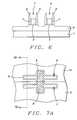
- a thermal oxidation procedureis performed at a temperature between about 700 to 1000° C., in an oxygen-steam ambient, resulting in the formation of silicon dioxide gate insulator layer 7 , on both sides of NMOS fin shape 5 , and PMOS fin shape 6 .
- Silicon dioxide gate insulator layer 7at a thickness between about 10 to 100 Angstroms, is schematically shown, in cross-sectional style in FIG. 3B.
- a top view of the fin shaped structuresis schematically shown in FIG. 3 A.
- a conductive layersuch as a doped polysilicon layer, a metal layer, or a metal silicide layer, is next deposited via chemical vapor deposition (CVD), or via plasma vapor deposition (PVD), procedures, to a thickness between about 100 to 3000 Angstroms.
- CVDchemical vapor deposition
- PVDplasma vapor deposition
- the metal layer optioncan be exercised using aluminum, aluminum-copper, tungsten, or tantalum, while the metal silicide option can employed using a layer such tungsten silicide, titanium silicide, tantalum silicide, nickel silicide, cobalt silicide, or zirconium silicide.
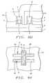
- a photoresist shapeis used as an etch mask to allow an anisotropic RIE procedure, using Cl 2 or SF 6 as an etchant, to define gate structure 8 .
- Thisis schematically shown as a top view in FIG. 4A, while a cross-sectional view of gate structure 8 , is schematically shown in FIG. 4 B.
- Gate structure 8traversing both fin shapes, and with gate insulator residing on both sides of the fin shapes, results in a double gate FINFET structure 5 , which will subsequently be processed to evolve as a double gate NMOS FINFET device, and results in a double gate FINFET structure 6 , which will subsequently be processed to form a double gate PMOS FINFET device.
- FIG. 4Ca cross-sectional view of non-gate regions, regions in which the conductive layer was removed, shows portions of the undoped SOI shapes, not covered by gate structure 8 .
- the photoresist shape used for definition of the conductive gate structureis removed via plasma oxygen ashing.
- a silicon nitride sidewall spacerhas to be employed.
- a silicon nitride layeris deposited via LPCVD or PECVD procedures, to a thickness between about 300 to 5000 Angstroms.
- An anisotropic RIE procedure, using CF 4 or Cl 2 as an etchant,is used to define silicon nitride spacers 9 , on the sides of the FINFET shapes, as well as on the sides of gate structure 8 . This is schematically shown as a top view in FIG. 5A, while FIGS. 5B and 5C, schematically show the definition of the silicon nitride spacers on FINFET shapes and on the gate structure in cross-sectional style.
- silicon nitride spacers 9on the sides of the FINFET shapes, as previously shown in FIG. 5C, allow selective removal of insulator shapes 4 , from the FINFET shapes to be accomplished, exposing the top surface of SOI shape 3 , in FINFET shape 5 , to be used for subsequent accommodation of an NMOS FINFET source/drain region, and exposing the top surface of SOI shape 3 , in FINFET shape 6 , to be used for subsequent accommodation of a PMOS FINFET source/drain region.
- the anisotropic RIE procedure used to remove insulator shapes 4is performed using CHF 3 as a selective etchant for silicon oxide. This procedure also removes top portions of insulator layer 2 , not covered by FINFET or gate structures. Silicon nitride spacers 9 , protected silicon dioxide gate insulator layer 7 , during this RIIE procedure.
- a borosilicate glass (BSG), layer 10is next deposited at a thickness between about 100 to 2000 Angstroms, via PECVD or LPCVD procedures.
- the weight percent of B 2 O 3 in BSG layer 10is between about 3 to 10%.
- Photoresist shape 11schematically shown in cross-sectional style in FIG. 7B, is used as a mask to allow removal of a portion of BSG layer 10 , in a region to be used to accommodate a subsequent NMOS FINFET device, to be accomplished.
- Removal of the exposed portion of BSG layer 10is achieved via a RIE procedure using CHF 3 as an etchant, or via a wet etch procedure using a buffered hydrofluoric (BHF) acid solution as an etchant.
- a top view showing BSG layer only overlying a subsequent PMOS FINFET device region,is schematically shown in FIG. 7 A.
- PSG layer 12After removal of photoresist shape 11 , via plasma oxygen ashing procedures, phosphosilicate glass (PSG) layer 12 , is deposited at a thickness between about 100 to 20000 Angstroms via LPCVD or PECVD procedures. The weight percent of P 2 O 5 in PSG layer 12 , is between about 3 to 10%.
- a first portion of PSG layer 12directly overlays only a region to be used to accommodate an NMOS FINFET device, shown schematically in cross-sectional style in FIG. 8B, while a second portion of PSG layer overlays BSG layer 10 , in a subsequent PMOS FINFET device region. This is also schematically shown as a top view using FIG. 8 A.
- An anneal procedureis next performed at a temperature between about 700 to 1000° C., for a time between about 1 to 60 min, in a conventional furnace, or via use of rapid thermal anneal (RTA) procedures.
- the anneal procedureallows the doping of the exposed SOI shapes which directly underlay the doped insulator layer, resulting in doped source/drain regions.
- the portion of FINFET shape 5 , underlying PSG layer 12is now N type source/drain region 40
- the portions of FINFET shape 6underlying BSG layer 10
- P type source/drain region 30This is schematically shown in cross-sectional style in FIG. 9B, and as a top view using FIG. 9 A. Therefore a desired NMOS FINFET device, featuring N type source/drain region 40 , and a desired PMOS FINFET device, featuring P type source/drain region 30 , is defined in the same SOI layer.
- Removal of PSG layer 12 , and of BSG layer 10is next addressed using a BBF acid solution, exposing the top surface of N type source/drain region 40 , and of P type source/drain region 30 .
- Selective deposition of a metal layeris next performed resulting in metal shapes 13 , overlying the doped source/drain regions.
- the presence of metal shapes 13allow a reduction in source/drain resistance to be realized.
- a metal layersuch as tungsten can be used for the selective deposition procedure, performed via CVD procedures at temperature between about 500 to 1000° C., using tungsten hexafluoride as a source. The result of this procedure is schematically shown, in cross-sectional style in FIG. 10 .
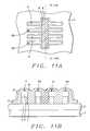
- Another embodiment of this inventionentails the reduction of gate resistance via filling of the spaces between FINFET shapes with the conductive metal layer used for definition of gate structure 9 .
- Thiscan be accomplished via use of dummy FINFET shapes 50 , defined adjacent to, and in a direction parallel to, FINFET shapes 5 and 6 .
- the reduction in the space between FINFET shapes 5 and 6allows the conductive metal layer to completely fill the narrower spaces, thus reducing gate resistance.
- Thisis schematically shown as a top view in FIG. 1A, while FIG. 11B, schematically shows the cross-sectional view.
- An additional optioncan a decrease in spacing between FINFET shapes 5 and 6 , to a point in which the conductive metal layer completely fills the narrower space, without employing dummy FINFET shapes.
Landscapes
- Thin Film Transistor (AREA)
Abstract
Description
(1) Field of the Invention
The present invention relates to methods used to fabricate semiconductor devices, and more specifically to a method used to fabricate a fin type field effect transistor (FINFET) device on a semiconductor substrate.
(2) Description of Prior Art
Micro-miniaturization, the ability to fabricate semiconductor devices comprised with sub-micron features, has allowed the performance of devices comprised with the sub-micron features to be increased. In addition the use of sub-micron features has allowed the attainment of smaller semiconductor chips to be realized, still providing device density equal to, or greater than, counterpart semiconductor chips formed with larger features, therefore allowing a greater number of semiconductor chips to be obtained from a specific size starting silicon wafer thus reducing the processing costs for a specific semiconductor chip. However as device features shrink specific parameters such as short channel effects, punch through, and leakage currents become more prevalent for devices formed with sub-micron features than for counterparts formed with larger features. The ability to fabricate a FINFET type device entirely in a silicon in insulator (SOI) layer, has allowed miniaturization of device features to be successfully accomplished with less risk of the yield degrading phenomena such as short channel effects, punch through leakages, and leakage current, when compared to counterpart devices formed in a semiconductor substrate. In addition the FINFET device, formed on an insulator layer, results in less junction capacitance, thus increased performance, when compared to the above counterpart devices formed in the semiconductor material.
The use of FINFET type devices however has mainly been applied to a single type metal oxide semiconductor field effect transistor (MOSFET), device, either an N channel (NMOS), device, or a P channel (PMOS), device. The ability to fabricate a complimentary metal oxide semiconductor (CMOS), device, comprised with both NMOS and PMOS devices, has been difficult to achieve for FINFET type devices. This invention will describe a novel process sequence in which the attractive advantages of FINFET devices can be realized for both NMOS and PMOS elements, formed in the same SOI layer. In addition this invention will describe additional process sequences allowing source/drain, as well as gate resistances for the FINFET device, to be reduced, thus providing additional performance enhancements. Prior art, such as Wu, in U.S. Pat. No. 6,010,934, Wu, in U.S. Pat. No. 6,117,711, and Muller et al, in U.S. Pat. No. 6,252,284 B1, describe methods of forming FIN type devices, however none of these prior arts describe the novel process sequence of this present invention in which a NMOS and a PMOS FINFET device are formed in the same SOI layer.
It is an object of this invention to fabricate both an NMOS FINFET, and a PMOS FINFET device in the same SOI layer.
It is another object of this invention to dope source/drain regions of both the NMOS and PMOS elements of the CMOS FINFET device, via out diffusion from overlying doped insulator layers.
It is still another object of this invention to decrease FINFET source/drain resistance via use of a selectively deposited, overlying metal layer.
It is still yet another object of this invention to reduce FINFET gate resistance via use of dummy silicon fins, or via a reduction in spacing between the silicon fins.
In accordance with the present invention a method of forming both NMOS and PMOS FINFET devices in the same SOI layer, is described. Fin type structures used to accommodate a subsequent NMOS FINFET device and a subsequent PMOS device, are formed in an SOI layer, each comprised with an overlying insulator shape. After formation of a gate insulator layer on the sides of the FIN type structures, a conductive gate structure is defined, normal in direction to, and traversing the FIN type structures. Insulator spacers are formed on the sides of the gate structure as well as on the sides of the insulator shape—FIN type structures. Removal of the insulator shapes expose top surfaces of SOI for the portions of FIN type structures not covered by the conductive gate structure. An N type doped insulator layer is formed overlying a first FIN type structure, to be used for the NMOS FINFET device, while a P type doped insulator layer is provided overlying the second FIN type structure to be used for the PMOS FINFET device. An anneal procedure results in an NMOS FINFET device, with the exposed portions of the first FIN type structure now an N type source/drain region, and results in a PMOS FINFET device, with the exposed portions of the second FIN type structure now a P type source/drain region. After removal of the doped insulator layers, selective metal deposition on the top surface of both N type, and P type source/drain regions is performed.
A second embodiment of this invention entails the use of dummy fin structures located between the NMOS and PMOS fin structures, allowing the deposition of the material used for the conductive gate to fill the spaces between the fin structures, thus reducing gate resistance when compared to counterparts in which the conductive gate material only contoured the fin type structures.
The object and other advantages of this invention are best described in the preferred embodiment with reference to the attached drawings that include:
FIGS. 1,2,3B,4B,4C,5B,5C,6,7B,8B,9B,10, and11B which schematically, in cross-sectional style, describe key fabrication stages used for formation of both NMOS and PMOS FINFET devices in the same SOI layer.
FIGS. 3A,4A,5A,7A,8A,9A, and11A which schematically show a top view of the FINFET device at specific stages of fabrication.
The method of forming an NMOS FINFET device, and a PMOS FINFET device, in the same SOI layer, featuring reductions in source/drain and gate resistance, will now be described in detail.Semiconductor substrate 1, comprised of single crystalline silicon with a <100> crystallographic orientation, is used and schematically shown in FIG.1.Silicon layer 3, the silicon component of an SOI layer, is formed via oxygen implantation into a portion ofsemiconductor substrate 1, followed by an anneal procedure which results in the formation ofinsulator layer 2, underlying non-implanted, and non-oxidizedsilicon layer 3.Insulator layer 2, is comprised of silicon dioxide at a thickness between about 100 to 1000 Angstroms, whileSOI layer 3, the remaining top portion ofsemiconductor substrate 1, overlyinginsulator layer 2, is maintained at a thickness between about 50 to 5000 Angstroms. If desired the SOI configuration can be obtained via bonding of a first semiconductor substrate to the top surface of an insulator layer located on a second semiconductor substrate. Removal of the bottom portion of the second semiconductor substrate via chemical mechanical polishing (CMP), procedures, results in a remaining portion of the second semiconductor substrate,SOI layer 3, oninsulator layer 2, of the first semiconductor substrate, again resulting in the desired SOI configuration.Insulator layer 4, comprised of silicon oxide at a thickness between about 50 to 5000 Angstroms, is next deposited onSOI layer 3, via low pressure chemical vapor deposition (LPCVD), or via plasma enhanced chemical vapor deposition (PECVD), procedures.
After removal ofphotoresist shapes 60, via plasma oxygen ashing procedures, a thermal oxidation procedure is performed at a temperature between about 700 to 1000° C., in an oxygen-steam ambient, resulting in the formation of silicon dioxidegate insulator layer 7, on both sides of NMOSfin shape 5, and PMOSfin shape 6. Silicon dioxidegate insulator layer 7, at a thickness between about 10 to 100 Angstroms, is schematically shown, in cross-sectional style in FIG. 3B. A top view of the fin shaped structures is schematically shown in FIG.3A.
A conductive layer such as a doped polysilicon layer, a metal layer, or a metal silicide layer, is next deposited via chemical vapor deposition (CVD), or via plasma vapor deposition (PVD), procedures, to a thickness between about 100 to 3000 Angstroms. The metal layer option can be exercised using aluminum, aluminum-copper, tungsten, or tantalum, while the metal silicide option can employed using a layer such tungsten silicide, titanium silicide, tantalum silicide, nickel silicide, cobalt silicide, or zirconium silicide. A photoresist shape, not shown in the drawings, is used as an etch mask to allow an anisotropic RIE procedure, using Cl2or SF6as an etchant, to definegate structure 8. This is schematically shown as a top view in FIG. 4A, while a cross-sectional view ofgate structure 8, is schematically shown in FIG.4B.Gate structure 8, traversing both fin shapes, and with gate insulator residing on both sides of the fin shapes, results in a doublegate FINFET structure 5, which will subsequently be processed to evolve as a double gate NMOS FINFET device, and results in a doublegate FINFET structure 6, which will subsequently be processed to form a double gate PMOS FINFET device. FIG. 4C, a cross-sectional view of non-gate regions, regions in which the conductive layer was removed, shows portions of the undoped SOI shapes, not covered bygate structure 8. The photoresist shape used for definition of the conductive gate structure is removed via plasma oxygen ashing.
To subsequently form N type and P type source/drain regions in the undoped portions of the SOI shapes, or in the portions ofFINFET structure 5, andFINFET structure 6, not covered by gate structures, a silicon nitride sidewall spacer has to be employed. A silicon nitride layer is deposited via LPCVD or PECVD procedures, to a thickness between about 300 to 5000 Angstroms. An anisotropic RIE procedure, using CF4or Cl2as an etchant, is used to definesilicon nitride spacers 9, on the sides of the FINFET shapes, as well as on the sides ofgate structure 8. This is schematically shown as a top view in FIG. 5A, while FIGS. 5B and 5C, schematically show the definition of the silicon nitride spacers on FINFET shapes and on the gate structure in cross-sectional style.
The presence ofsilicon nitride spacers 9, on the sides of the FINFET shapes, as previously shown in FIG. 5C, allow selective removal of insulator shapes4, from the FINFET shapes to be accomplished, exposing the top surface ofSOI shape 3, inFINFET shape 5, to be used for subsequent accommodation of an NMOS FINFET source/drain region, and exposing the top surface ofSOI shape 3, inFINFET shape 6, to be used for subsequent accommodation of a PMOS FINFET source/drain region. The anisotropic RIE procedure used to removeinsulator shapes 4, is performed using CHF3as a selective etchant for silicon oxide. This procedure also removes top portions ofinsulator layer 2, not covered by FINFET or gate structures.Silicon nitride spacers 9, protected silicon dioxidegate insulator layer 7, during this RIIE procedure.
A borosilicate glass (BSG),layer 10, is next deposited at a thickness between about 100 to 2000 Angstroms, via PECVD or LPCVD procedures. The weight percent of B2O3inBSG layer 10, is between about 3 to 10%.Photoresist shape 11, schematically shown in cross-sectional style in FIG. 7B, is used as a mask to allow removal of a portion ofBSG layer 10, in a region to be used to accommodate a subsequent NMOS FINFET device, to be accomplished. Removal of the exposed portion ofBSG layer 10, is achieved via a RIE procedure using CHF3as an etchant, or via a wet etch procedure using a buffered hydrofluoric (BHF) acid solution as an etchant. A top view showing BSG layer only overlying a subsequent PMOS FINFET device region, is schematically shown in FIG.7A.
After removal ofphotoresist shape 11, via plasma oxygen ashing procedures, phosphosilicate glass (PSG)layer 12, is deposited at a thickness between about 100 to 20000 Angstroms via LPCVD or PECVD procedures. The weight percent of P2O5inPSG layer 12, is between about 3 to 10%. A first portion ofPSG layer 12, directly overlays only a region to be used to accommodate an NMOS FINFET device, shown schematically in cross-sectional style in FIG. 8B, while a second portion of PSG layer overlaysBSG layer 10, in a subsequent PMOS FINFET device region. This is also schematically shown as a top view using FIG.8A.
An anneal procedure is next performed at a temperature between about 700 to 1000° C., for a time between about 1 to 60 min, in a conventional furnace, or via use of rapid thermal anneal (RTA) procedures. The anneal procedure allows the doping of the exposed SOI shapes which directly underlay the doped insulator layer, resulting in doped source/drain regions. The portion ofFINFET shape 5, underlyingPSG layer 12, is now N type source/drain region 40, while the portions ofFINFET shape 6, underlyingBSG layer 10, is now P type source/drain region 30. This is schematically shown in cross-sectional style in FIG. 9B, and as a top view using FIG.9A. Therefore a desired NMOS FINFET device, featuring N type source/drain region 40, and a desired PMOS FINFET device, featuring P type source/drain region 30, is defined in the same SOI layer.
Removal ofPSG layer 12, and ofBSG layer 10, is next addressed using a BBF acid solution, exposing the top surface of N type source/drain region 40, and of P type source/drain region 30. Selective deposition of a metal layer, at a thickness between about 100 to 3000 Angstroms, is next performed resulting inmetal shapes 13, overlying the doped source/drain regions. The presence of metal shapes13, allow a reduction in source/drain resistance to be realized. A metal layer such as tungsten can be used for the selective deposition procedure, performed via CVD procedures at temperature between about 500 to 1000° C., using tungsten hexafluoride as a source. The result of this procedure is schematically shown, in cross-sectional style in FIG.10.
Another embodiment of this invention entails the reduction of gate resistance via filling of the spaces between FINFET shapes with the conductive metal layer used for definition ofgate structure 9. This can be accomplished via use of dummy FINFET shapes50, defined adjacent to, and in a direction parallel to, FINFET shapes5 and6. The reduction in the space between FINFET shapes5 and6, as a result of dummy FINFET shapes50, allows the conductive metal layer to completely fill the narrower spaces, thus reducing gate resistance. This is schematically shown as a top view in FIG. 1A, while FIG. 11B, schematically shows the cross-sectional view. An additional option can a decrease in spacing between FINFET shapes5 and6, to a point in which the conductive metal layer completely fills the narrower space, without employing dummy FINFET shapes.
While this invention has been particularly shown and described with reference to, the preferred embodiments thereof, it will be understood by those skilled in the art that various changes in form and details may be made without departing from the spirit and scope of this invention.
Claims (26)
1. A method of forming a complimentary metal oxide semiconductor (CMOS), device in a silicon on insulator (SOI), layer, comprising the steps of:
forming said SOI layer on a semiconductor substrate;
forming an insulator layer on said SOI layer;
defining a first fin type structure in said insulator layer and in said SOI layer, and
forming a second fin type structure in said insulator layer and in said SOI layer;
growing a gate insulator layer on sides of said first fin type structure and on the sides of said second fin type structure;
forming a gate structure traversing, and normal in direction to, fin type structures;
forming an insulator spacer on sides of portions of said fin type structures not covered by said gate structure, and on sides of said gate structure;
forming a first doped insulator layer overlying a first SOI shape, and forming a second doped insulator layer overlying a second SOI shape;
performing an anneal procedure to create a first source/drain region of a first conductivity type in said first SOI shape, and to create a second source/drain region of a second conductivity shape in said second SOI shape;
removing said first doped insulator layer and said second doped insulator layer; and
forming metal shapes on said first source/drain region and on said second source/drain region, resulting in said CMOS device comprised of a first metal oxide semiconductor (MOS), device of a first channel type, featuring said first source/drain region, and comprised of a second MOS device of a second channel type, featuring said second source/drain region.
2. The method ofclaim 1 , wherein said SOI layer is formed at a thickness between about 50 to 5000 Angstroms.
3. The method ofclaim 1 , wherein said insulator layer is a silicon oxide layer obtained at a thickness between about 50 to 5000 Angstroms via LPCVD or PECVD procedures.
4. The method ofclaim 1 , wherein the width of said first fin type structure, and of said second fin type structure, is between about 50 to 1000 Angstroms.
5. The method ofclaim 1 , wherein said gate insulator layer is a silicon dioxide layer, obtained at a thickness between about 10 to 100 Angstroms via a thermal oxidation procedure performed at a temperature between about 700 to 1000° C., in an oxygen-steam ambient.
6. The method ofclaim 1 , wherein said gate structure is defined from a conductive layer chosen from a group containing doped polysilicon, aluminum, aluminum-copper, tungsten, tantalum, tungsten silicide, tantalum silicide, nickel silicide, cobalt silicide, or titanium silicide.
7. The method ofclaim 1 , wherein the thickness of said gate structure is between about 100 to 3000 Angstroms.
8. The method ofclaim 1 , wherein said insulator spacer is a silicon nitride spacer, formed at a thickness between about 300 to 5000 Angstroms.
9. The method ofclaim 1 , wherein said first doped insulator layer is a borosilicate glass (BSG), layer, obtained via LPCVD or PECVD procedures at a thickness between about 100 to 2000 Angstroms, with a B2O3weight percent between about 3 to 10%.
10. The method ofclaim 1 , wherein said second doped insulator layer is a phosphosilicate glass (PSG), layer, obtained via LPCVD or PECVD procedures at a thickness between about 100 to 2000 Angstroms, with a P2O5weight percent between about 3 to 10%.
11. The method ofclaim 1 , wherein said anneal procedure is performed in a conventional furnace, or via a rapid thermal anneal procedure, at a temperature between about 700 to 1000° C., for a time between about 1 to 60 min.
12. The method ofclaim 1 , wherein said first doped insulator layer and said second doped insulator layer are removed using a buffered hydrofluoric acid solution.
13. The method ofclaim 1 , wherein said metal shapes formed on said first source/drain region and on said second source/drain region, are comprised of tungsten.
14. The method ofclaim 1 , wherein said metal shapes are tungsten metal shapes, obtained at a thickness between about 100 to 3000 Angstroms, via selective chemical vapor deposition procedures performed at a temperature between about 500 to 1000° C., using tungsten hexafluoride as a source.
15. A method of forming a FINFET CMOS device in a silicon on insulator (SOI), layer, comprising the steps of:
forming said SOI layer on a semiconductor substrate;
depositing a silicon oxide layer on said SOI layer;
performing a first anisotropic reactive ion etch (RIE) procedure to define a first fin type structure in said silicon oxide layer and in said SOI layer, and to define a second fin type structure in said silicon oxide layer and in said SOI layer, with said second fin type structure parallel in direction with said first fin type structure;
growing a silicon dioxide gate insulator layer on sides of fin type structures;
depositing a conductive layer;
performing a second anisotropic RIE procedure to form a conductive gate structure traversing, and normal in direction to, said fin type structures;
depositing a silicon nitride layer;
performing a third anisotropic RIE procedure to form a silicon nitride spacer on sides of the portions of said fin type structures not covered by said conductive gate structure, and on sides of said conductive gate structure;
removing said silicon oxide layer from portions of said fin type structures not covered by said conductive gate structure, exposing a first SOI shape of said first fin type structure, and exposing a second SOI shape of said second fin type structure;
depositing a first doped insulator layer;
removing said first doped insulator layer from a region overlying said second fin type structure;
depositing a second doped insulator layer directly overlying said second fin type structure, while said second doped insulator layer overlays said first doped insulator layer in a region in which said first doped insulator layer directly overlays said first fin type structure;
performing an anneal procedure to create a first source/drain region, of a first conductivity type, in said first SOI shape of said first fin type structure, and to create a second source/drain region, of a second conductivity type, in said second SOT shape of said second fin type structure;
removing said first doped insulator layer and said second doped insulator layer; and
selectively depositing tungsten on source/drain regions resulting in said FINFET CMOS device, featuring a first metal oxide semiconductor (MOS), device of a first channel type, comprised with said first source/drain region, and featuring a second MOS device of a second channel type, comprised with said second source/drain region.
16. The method ofclaim 15 , wherein said SOI layer is formed at a thickness between about 50 to 5000 Angstroms.
17. The method ofclaim 15 , wherein said silicon oxide layer is obtained at a thickness between about 50 to 5000 Angstroms via LPCVD or PECVD procedures.
18. The method ofclaim 15 , wherein the width of said first fin structure and of said second fin structure is between about 50 to 1000 Angstroms.
19. The method ofclaim 15 , wherein said silicon dioxide gate insulator layer is obtained at a thickness between about 10 to 100 Angstroms via a thermal oxidation procedure performed at a temperature between about 700 to 1000° C., in an oxygen-steam ambient.
20. The method ofclaim 15 , wherein said conductive layer, used for said conductive gate structure, is chosen from a group containing doped polysilicon, aluminum, aluminum-copper, tungsten, tantalum, tungsten silicide, tantalum silicide, nickel silicide, cobalt silicide, or titanium silicide.
21. The method ofclaim 15 , wherein said silicon nitride spacer is formed at a thickness between about 300 to 5000 Angstroms.
22. The method ofclaim 15 , wherein said first doped insulator layer is a borosilicate glass (BSG), layer, obtained via LPCVD or PECVD procedures, at a thickness between about 100 to 2000 Angstroms, with a B2O3weight percent between about 3 to 10%.
23. The method ofclaim 15 , wherein said second doped insulator layer is a phosphosilicate glass (PSG), layer, obtained via LPCVD or PECVD procedures, at a thickness between about 100 to 2000 Angstroms, with a P2O5weight percent between about 3 to 10%.
24. The method ofclaim 15 , wherein said anneal procedure is performed in a conventional furnace, or via a rapid thermal anneal procedure, at a temperature between about 700 to 1000° C., for a time between about 1 to 60 min.
25. The method ofclaim 15 , wherein said first doped insulator layer and said second doped insulator layer are removed using a buffered hydrofluoric acid solution.
26. The method ofclaim 15 , wherein said tungsten layer is selectively deposited to a thickness between about 100 to 3000 Angstroms, via selective chemical vapor deposition procedures, performed at a temperature between about 500 to 1000° C., using tungsten hexafluoride as a source.
Priority Applications (2)
| Application Number | Priority Date | Filing Date | Title |
|---|---|---|---|
| US10/235,253US6770516B2 (en) | 2002-09-05 | 2002-09-05 | Method of forming an N channel and P channel FINFET device on the same semiconductor substrate |
| US10/831,868US7187046B2 (en) | 2002-09-05 | 2004-04-26 | Method of forming an N channel and P channel finfet device on the same semiconductor substrate |
Applications Claiming Priority (1)
| Application Number | Priority Date | Filing Date | Title |
|---|---|---|---|
| US10/235,253US6770516B2 (en) | 2002-09-05 | 2002-09-05 | Method of forming an N channel and P channel FINFET device on the same semiconductor substrate |
Related Child Applications (1)
| Application Number | Title | Priority Date | Filing Date |
|---|---|---|---|
| US10/831,868DivisionUS7187046B2 (en) | 2002-09-05 | 2004-04-26 | Method of forming an N channel and P channel finfet device on the same semiconductor substrate |
Publications (2)
| Publication Number | Publication Date |
|---|---|
| US20040048424A1 US20040048424A1 (en) | 2004-03-11 |
| US6770516B2true US6770516B2 (en) | 2004-08-03 |
Family
ID=31990491
Family Applications (2)
| Application Number | Title | Priority Date | Filing Date |
|---|---|---|---|
| US10/235,253Expired - Fee RelatedUS6770516B2 (en) | 2002-09-05 | 2002-09-05 | Method of forming an N channel and P channel FINFET device on the same semiconductor substrate |
| US10/831,868Expired - LifetimeUS7187046B2 (en) | 2002-09-05 | 2004-04-26 | Method of forming an N channel and P channel finfet device on the same semiconductor substrate |
Family Applications After (1)
| Application Number | Title | Priority Date | Filing Date |
|---|---|---|---|
| US10/831,868Expired - LifetimeUS7187046B2 (en) | 2002-09-05 | 2004-04-26 | Method of forming an N channel and P channel finfet device on the same semiconductor substrate |
Country Status (1)
| Country | Link |
|---|---|
| US (2) | US6770516B2 (en) |
Cited By (84)
| Publication number | Priority date | Publication date | Assignee | Title |
|---|---|---|---|---|
| US20040092060A1 (en)* | 2001-09-27 | 2004-05-13 | Gambino Jeffrey P. | FIN field effect transistor with self-aligned gate |
| US20040198031A1 (en)* | 2003-04-03 | 2004-10-07 | Ming-Ren Lin | Method for forming structures in finfet devices |
| US20050001273A1 (en)* | 2003-07-01 | 2005-01-06 | International Business Machines Corporation | Integrated circuit having pairs of parallel complementary finfets |
| US20050009285A1 (en)* | 2002-09-06 | 2005-01-13 | Scott Luning | Semiconductor component and method of manufacture |
| US6855588B1 (en)* | 2003-10-07 | 2005-02-15 | United Microelectronics Corp. | Method of fabricating a double gate MOSFET device |
| US20050056888A1 (en)* | 2003-09-16 | 2005-03-17 | Jae-Man Youn | Double gate field effect transistor and method of manufacturing the same |
| US20050059194A1 (en)* | 2003-09-15 | 2005-03-17 | Chartered Semiconductor Manufacturing Ltd. | Method of forming double-gated silicon-on-insulator (SOI) transistors with corner rounding |
| US20050186738A1 (en)* | 2002-09-05 | 2005-08-25 | Infineon Technologies Ag | High-density NROM-FINFET |
| US6949768B1 (en)* | 2004-10-18 | 2005-09-27 | International Business Machines Corporation | Planar substrate devices integrated with finfets and method of manufacture |
| US20050237850A1 (en)* | 2003-10-02 | 2005-10-27 | Suman Datta | Method and apparatus for improving stability of a 6T CMOS SRAM cell |
| US20050242406A1 (en)* | 2003-06-27 | 2005-11-03 | Hareland Scott A | Nonplanar device with stress incorporation layer and method of fabrication |
| US20050258477A1 (en)* | 2004-05-19 | 2005-11-24 | Tomohiro Saito | Semiconductor device and method of manufacturing the same |
| US20060033095A1 (en)* | 2004-08-10 | 2006-02-16 | Doyle Brian S | Non-planar pMOS structure with a strained channel region and an integrated strained CMOS flow |
| US20060043502A1 (en)* | 2003-11-26 | 2006-03-02 | International Business Machines Corporation | Structure and method to fabricate finfet devices |
| US20060154423A1 (en)* | 2002-12-19 | 2006-07-13 | Fried David M | Methods of forming structure and spacer and related finfet |
| US20060177998A1 (en)* | 2003-09-03 | 2006-08-10 | Harrity & Snyder, L.L.P. | Fully silicided gate structure for finfet devices |
| US20060208300A1 (en)* | 2003-03-20 | 2006-09-21 | Junko Iwanaga | Finfet-type semiconductor device and method for fabricating the same |
| US20070018245A1 (en)* | 2005-07-06 | 2007-01-25 | Applied Intellectual Properties Co., Ltd. | Fringing field induced localized charge trapping memory |
| US20070063306A1 (en)* | 2005-09-22 | 2007-03-22 | Intel Corporation | Multiple crystal orientations on the same substrate |
| US20070131983A1 (en)* | 2005-12-13 | 2007-06-14 | Intel Corporation | Tri-gate integration with embedded floating body memory cell using a high-K dual metal gate |
| US20070134878A1 (en)* | 2005-12-09 | 2007-06-14 | Intel Corporation | Non-planar microelectronic device having isolation element to mitigate fringe effects and method to fabricate same |
| US20070138514A1 (en)* | 2005-12-21 | 2007-06-21 | Chang Peter L | Integration of planar and tri-gate devices on the same substrate |
| US20070148926A1 (en)* | 2005-12-28 | 2007-06-28 | Intel Corporation | Dual halo implant for improving short channel effect in three-dimensional tri-gate transistors |
| US20070231997A1 (en)* | 2006-03-31 | 2007-10-04 | Doyle Brian S | Stacked multi-gate transistor design and method of fabrication |
| US20070235763A1 (en)* | 2006-03-29 | 2007-10-11 | Doyle Brian S | Substrate band gap engineered multi-gate pMOS devices |
| US20070238273A1 (en)* | 2006-03-31 | 2007-10-11 | Doyle Brian S | Method of ion implanting for tri-gate devices |
| US20080081405A1 (en)* | 2006-09-29 | 2008-04-03 | Hynix Semiconductor Inc. | Method for fabricating a semiconductor device with a FinFET |
| US7361958B2 (en) | 2004-09-30 | 2008-04-22 | Intel Corporation | Nonplanar transistors with metal gate electrodes |
| US20080097346A1 (en)* | 2006-09-19 | 2008-04-24 | Alcon, Inc. | Trocar cannula |
| US20080121998A1 (en)* | 2006-09-15 | 2008-05-29 | Kavalieros Jack T | Apparatus and method for selectively recessing spacers on multi-gate devices |
| US7396711B2 (en) | 2005-12-27 | 2008-07-08 | Intel Corporation | Method of fabricating a multi-cornered film |
| US7425500B2 (en) | 2006-03-31 | 2008-09-16 | Intel Corporation | Uniform silicide metal on epitaxially grown source and drain regions of three-dimensional transistors |
| US7432557B1 (en) | 2003-07-08 | 2008-10-07 | Advanced Micro Devices, Inc. | FinFET device with multiple channels |
| US20080258228A1 (en)* | 2007-04-18 | 2008-10-23 | Harry Chuang | Contact Scheme for MOSFETs |
| US7442596B2 (en) | 2005-02-24 | 2008-10-28 | Samsung Electronics Co., Ltd. | Methods of manufacturing fin type field effect transistors |
| US7456476B2 (en) | 2003-06-27 | 2008-11-25 | Intel Corporation | Nonplanar semiconductor device with partially or fully wrapped around gate electrode and methods of fabrication |
| US20080296691A1 (en)* | 2007-05-30 | 2008-12-04 | Harry Chuang | Layout methods of integrated circuits having unit MOS devices |
| US7479421B2 (en) | 2005-09-28 | 2009-01-20 | Intel Corporation | Process for integrating planar and non-planar CMOS transistors on a bulk substrate and article made thereby |
| US7498225B1 (en) | 2003-12-04 | 2009-03-03 | Advanced Micro Devices, Inc. | Systems and methods for forming multiple fin structures using metal-induced-crystallization |
| US7518196B2 (en) | 2005-02-23 | 2009-04-14 | Intel Corporation | Field effect transistor with narrow bandgap source and drain regions and method of fabrication |
| US7525160B2 (en) | 2005-12-27 | 2009-04-28 | Intel Corporation | Multigate device with recessed strain regions |
| US7547637B2 (en) | 2005-06-21 | 2009-06-16 | Intel Corporation | Methods for patterning a semiconductor film |
| US7550333B2 (en) | 2004-10-25 | 2009-06-23 | Intel Corporation | Nonplanar device with thinned lower body portion and method of fabrication |
| US7579280B2 (en) | 2004-06-01 | 2009-08-25 | Intel Corporation | Method of patterning a film |
| US7679134B1 (en) | 2002-11-26 | 2010-03-16 | Globalfoundries | FinFET device with multiple fin structures |
| US7700470B2 (en) | 2006-09-22 | 2010-04-20 | Intel Corporation | Selective anisotropic wet etching of workfunction metal for semiconductor devices |
| US7736956B2 (en) | 2005-08-17 | 2010-06-15 | Intel Corporation | Lateral undercut of metal gate in SOI device |
| US20100155801A1 (en)* | 2008-12-22 | 2010-06-24 | Doyle Brian S | Integrated circuit, 1T-1C embedded memory cell containing same, and method of manufacturing 1T-1C memory cell for embedded memory application |
| US20100163945A1 (en)* | 2008-12-30 | 2010-07-01 | Kavalieros Jack T | Embedded memory cell and method of manufacturing same |
| US7781771B2 (en) | 2004-03-31 | 2010-08-24 | Intel Corporation | Bulk non-planar transistor having strained enhanced mobility and methods of fabrication |
| US20100244103A1 (en)* | 2009-03-30 | 2010-09-30 | International Business Machines Corporation | Structure and method of fabricating finfet |
| US7859053B2 (en) | 2004-09-29 | 2010-12-28 | Intel Corporation | Independently accessed double-gate and tri-gate transistors in same process flow |
| US7879675B2 (en) | 2005-03-14 | 2011-02-01 | Intel Corporation | Field effect transistor with metal source/drain regions |
| US7898041B2 (en) | 2005-06-30 | 2011-03-01 | Intel Corporation | Block contact architectures for nanoscale channel transistors |
| US7902014B2 (en) | 2005-09-28 | 2011-03-08 | Intel Corporation | CMOS devices with a single work function gate electrode and method of fabrication |
| US7915167B2 (en) | 2004-09-29 | 2011-03-29 | Intel Corporation | Fabrication of channel wraparound gate structure for field-effect transistor |
| US20110079852A1 (en)* | 2009-10-07 | 2011-04-07 | Taiwan Semiconductor Manufacturing Company, Ltd., ("Tsmc") | Method of fabricating a semiconductor device |
| US7989280B2 (en) | 2005-11-30 | 2011-08-02 | Intel Corporation | Dielectric interface for group III-V semiconductor device |
| US20110193141A1 (en)* | 2010-02-11 | 2011-08-11 | Taiwan Semiconductor Manufacturing Company, Ltd. | Method of fabricating a finfet device |
| US8084818B2 (en) | 2004-06-30 | 2011-12-27 | Intel Corporation | High mobility tri-gate devices and methods of fabrication |
| US20120138886A1 (en)* | 2010-12-01 | 2012-06-07 | Kuhn Kelin J | Silicon and silicon germanium nanowire structures |
| US8362566B2 (en) | 2008-06-23 | 2013-01-29 | Intel Corporation | Stress in trigate devices using complimentary gate fill materials |
| US8420459B1 (en) | 2011-10-20 | 2013-04-16 | International Business Machines Corporation | Bulk fin-field effect transistors with well defined isolation |
| US8617945B2 (en) | 2006-08-02 | 2013-12-31 | Intel Corporation | Stacking fault and twin blocking barrier for integrating III-V on Si |
| US8617961B1 (en) | 2012-07-18 | 2013-12-31 | International Business Machines Corporation | Post-gate isolation area formation for fin field effect transistor device |
| US8802512B2 (en) | 2013-01-11 | 2014-08-12 | International Business Machines Corporation | Overlap capacitance nanowire |
| US8809178B2 (en) | 2012-02-29 | 2014-08-19 | Globalfoundries Inc. | Methods of forming bulk FinFET devices with replacement gates so as to reduce punch through leakage currents |
| US8987794B2 (en) | 2011-12-23 | 2015-03-24 | Intel Coporation | Non-planar gate all-around device and method of fabrication thereof |
| US9012284B2 (en) | 2011-12-23 | 2015-04-21 | Intel Corporation | Nanowire transistor devices and forming techniques |
| US20150348966A1 (en)* | 2014-05-30 | 2015-12-03 | Semiconductor Manufacturing International (Shanghai) Corporation | Fin field-effct transistors and fabrication method thereof |
| US9287380B2 (en)* | 2005-12-30 | 2016-03-15 | Intel Corporation | Gate electrode having a capping layer |
| US9337307B2 (en) | 2005-06-15 | 2016-05-10 | Intel Corporation | Method for fabricating transistor with thinned channel |
| CN105679824A (en)* | 2014-11-18 | 2016-06-15 | 中芯国际集成电路制造(上海)有限公司 | Fin field effect transistor and fabrication method thereof |
| US9466361B2 (en) | 2008-05-22 | 2016-10-11 | Micron Technology, Inc. | Memory devices |
| US9564437B1 (en) | 2015-08-25 | 2017-02-07 | International Business Machines Corporation | Method and structure for forming FinFET CMOS with dual doped STI regions |
| US9576978B2 (en) | 2012-10-09 | 2017-02-21 | Samsung Electronics Co., Ltd. | Cells including at least one fin field effect transistor and semiconductor integrated circuits including the same |
| US9614006B2 (en) | 2007-05-01 | 2017-04-04 | Micron Technology, Inc. | Semiconductor constructions, and methods of forming cross-point memory arrays |
| US9647113B2 (en) | 2014-03-05 | 2017-05-09 | International Business Machines Corporation | Strained FinFET by epitaxial stressor independent of gate pitch |
| US20170148789A1 (en)* | 2015-10-20 | 2017-05-25 | International Business Machines Corporation | Effective device formation for advanced technology nodes with aggressive fin-pitch scaling |
| US9876097B2 (en) | 2016-06-14 | 2018-01-23 | International Business Machines Corporation | Selectively formed gate sidewall spacer |
| US10020378B2 (en) | 2016-09-22 | 2018-07-10 | International Business Machines Corporation | Self-aligned spacer for cut-last transistor fabrication |
| US10304940B1 (en)* | 2017-11-30 | 2019-05-28 | Intel Corporation | Gate cut and fin trim isolation for advanced integrated circuit structure fabrication |
| US10468412B2 (en) | 2016-06-28 | 2019-11-05 | International Business Machines Corporation | Formation of a semiconductor device with selective nitride grown on conductor |
| US11322601B2 (en) | 2017-11-30 | 2022-05-03 | Intel Corporation | Gate cut and fin trim isolation for advanced integrated circuit structure fabrication |
Families Citing this family (63)
| Publication number | Priority date | Publication date | Assignee | Title |
|---|---|---|---|---|
| US8222680B2 (en)* | 2002-10-22 | 2012-07-17 | Advanced Micro Devices, Inc. | Double and triple gate MOSFET devices and methods for making same |
| US6611029B1 (en)* | 2002-11-08 | 2003-08-26 | Advanced Micro Devices, Inc. | Double gate semiconductor device having separate gates |
| US7148526B1 (en)* | 2003-01-23 | 2006-12-12 | Advanced Micro Devices, Inc. | Germanium MOSFET devices and methods for making same |
| US6762483B1 (en)* | 2003-01-23 | 2004-07-13 | Advanced Micro Devices, Inc. | Narrow fin FinFET |
| US7259425B2 (en)* | 2003-01-23 | 2007-08-21 | Advanced Micro Devices, Inc. | Tri-gate and gate around MOSFET devices and methods for making same |
| US6894326B2 (en)* | 2003-06-25 | 2005-05-17 | International Business Machines Corporation | High-density finFET integration scheme |
| US6936882B1 (en)* | 2003-07-08 | 2005-08-30 | Advanced Micro Devices, Inc. | Selective silicidation of gates in semiconductor devices to achieve multiple threshold voltages |
| US7235436B1 (en)* | 2003-07-08 | 2007-06-26 | Advanced Micro Devices, Inc. | Method for doping structures in FinFET devices |
| US6812119B1 (en) | 2003-07-08 | 2004-11-02 | Advanced Micro Devices, Inc. | Narrow fins by oxidation in double-gate finfet |
| US7041601B1 (en)* | 2003-09-03 | 2006-05-09 | Advanced Micro Devices, Inc. | Method of manufacturing metal gate MOSFET with strained channel |
| US6855989B1 (en) | 2003-10-01 | 2005-02-15 | Advanced Micro Devices, Inc. | Damascene finfet gate with selective metal interdiffusion |
| US7029958B2 (en)* | 2003-11-04 | 2006-04-18 | Advanced Micro Devices, Inc. | Self aligned damascene gate |
| KR100702552B1 (en)* | 2003-12-22 | 2007-04-04 | 인터내셔널 비지네스 머신즈 코포레이션 | Automated Layer Creation Method and Device for Double Gate FFT Design |
| US8217450B1 (en) | 2004-02-03 | 2012-07-10 | GlobalFoundries, Inc. | Double-gate semiconductor device with gate contacts formed adjacent sidewalls of a fin |
| KR100585131B1 (en)* | 2004-02-20 | 2006-06-01 | 삼성전자주식회사 | Semiconductor device and manufacturing method thereof |
| WO2005091374A1 (en)* | 2004-03-19 | 2005-09-29 | Nec Corporation | Semiconductor device and method for manufacturing same |
| KR100605104B1 (en)* | 2004-05-04 | 2006-07-26 | 삼성전자주식회사 | Fin-Pet device and its manufacturing method |
| US7262104B1 (en) | 2004-06-02 | 2007-08-28 | Advanced Micro Devices, Inc. | Selective channel implantation for forming semiconductor devices with different threshold voltages |
| US7045862B2 (en)* | 2004-06-11 | 2006-05-16 | International Business Machines Corporation | Method and structure for providing tuned leakage current in CMOS integrated circuit |
| US7611943B2 (en)* | 2004-10-20 | 2009-11-03 | Texas Instruments Incorporated | Transistors, integrated circuits, systems, and processes of manufacture with improved work function modulation |
| JP2006308873A (en)* | 2005-04-28 | 2006-11-09 | Fuji Photo Film Co Ltd | Silver halide color photographic sensitive material |
| JP2008010503A (en)* | 2006-06-27 | 2008-01-17 | Toshiba Corp | Semiconductor memory device and manufacturing method thereof |
| CN101490822B (en)* | 2006-07-11 | 2011-03-16 | Nxp股份有限公司 | Semiconductor device and manufacturing method thereof |
| US7960234B2 (en)* | 2007-03-22 | 2011-06-14 | Texas Instruments Incorporated | Multiple-gate MOSFET device and associated manufacturing methods |
| US7723786B2 (en)* | 2007-04-11 | 2010-05-25 | Ronald Kakoschke | Apparatus of memory array using FinFETs |
| US7795669B2 (en)* | 2007-05-30 | 2010-09-14 | Infineon Technologies Ag | Contact structure for FinFET device |
| US7692254B2 (en)* | 2007-07-16 | 2010-04-06 | International Business Machines Corporation | Fin-type field effect transistor structure with merged source/drain silicide and method of forming the structure |
| US20090050975A1 (en)* | 2007-08-21 | 2009-02-26 | Andres Bryant | Active Silicon Interconnect in Merged Finfet Process |
| US7888736B2 (en)* | 2007-08-29 | 2011-02-15 | International Business Machines Corporation | MUGFET with optimized fill structures |
| US7736965B2 (en)* | 2007-12-06 | 2010-06-15 | International Business Machines Corporation | Method of making a FinFET device structure having dual metal and high-k gates |
| US7763943B2 (en)* | 2007-12-26 | 2010-07-27 | Intel Corporation | Reducing external resistance of a multi-gate device by incorporation of a partial metallic fin |
| US8330170B2 (en)* | 2008-12-05 | 2012-12-11 | Micron Technology, Inc. | Semiconductor device structures including transistors with energy barriers adjacent to transistor channels and associated methods |
| US8017427B2 (en) | 2008-12-31 | 2011-09-13 | Omnivision Technologies, Inc. | Backside-illuminated (BSI) image sensor with backside diffusion doping |
| US7977174B2 (en)* | 2009-06-08 | 2011-07-12 | Globalfoundries Inc. | FinFET structures with stress-inducing source/drain-forming spacers and methods for fabricating the same |
| US8980719B2 (en) | 2010-04-28 | 2015-03-17 | Taiwan Semiconductor Manufacturing Company, Ltd. | Methods for doping fin field-effect transistors |
| US8482073B2 (en)* | 2010-03-25 | 2013-07-09 | Taiwan Semiconductor Manufacturing Company, Ltd. | Integrated circuit including FINFETs and methods for forming the same |
| US8629478B2 (en)* | 2009-07-31 | 2014-01-14 | Taiwan Semiconductor Manufacturing Company, Ltd. | Fin structure for high mobility multiple-gate transistor |
| US8440517B2 (en) | 2010-10-13 | 2013-05-14 | Taiwan Semiconductor Manufacturing Company, Ltd. | FinFET and method of fabricating the same |
| US8729627B2 (en)* | 2010-05-14 | 2014-05-20 | Taiwan Semiconductor Manufacturing Company, Ltd. | Strained channel integrated circuit devices |
| US8373229B2 (en)* | 2010-08-30 | 2013-02-12 | Taiwan Semiconductor Manufacturing Company, Ltd. | Gate controlled bipolar junction transistor on fin-like field effect transistor (FinFET) structure |
| US8431453B2 (en) | 2011-03-31 | 2013-04-30 | Taiwan Semiconductor Manufacturing Company, Ltd. | Plasma doping to reduce dielectric loss during removal of dummy layers in a gate structure |
| CN103035711B (en)* | 2011-09-30 | 2016-04-20 | 中国科学院微电子研究所 | Semiconductor structure and manufacturing method thereof |
| US8604518B2 (en)* | 2011-11-30 | 2013-12-10 | Taiwan Semiconductor Manufacturing Company, Ltd. | Split-channel transistor and methods for forming the same |
| US8723223B2 (en)* | 2011-11-30 | 2014-05-13 | Taiwan Semiconductor Manufacturing Company, Ltd. | Hybrid Fin field-effect transistors |
| US9105744B2 (en) | 2012-03-01 | 2015-08-11 | Taiwan Semiconductor Manufacturing Company, Ltd. | Semiconductor devices having inactive fin field effect transistor (FinFET) structures and manufacturing and design methods thereof |
| US10515956B2 (en) | 2012-03-01 | 2019-12-24 | Taiwan Semiconductor Manufacturing Company | Semiconductor devices having Fin Field Effect Transistor (FinFET) structures and manufacturing and design methods thereof |
| CN103383965B (en)* | 2012-05-04 | 2016-01-20 | 台湾积体电路制造股份有限公司 | Mixing fin formula field effect transistor |
| US8569152B1 (en) | 2012-06-04 | 2013-10-29 | International Business Machines Corporation | Cut-very-last dual-epi flow |
| US8906759B2 (en) | 2013-02-25 | 2014-12-09 | International Business Machines Corporation | Silicon nitride gate encapsulation by implantation |
| US8703557B1 (en)* | 2013-04-15 | 2014-04-22 | Globalfoundries Inc. | Methods of removing dummy fin structures when forming finFET devices |
| US9059043B1 (en)* | 2014-02-11 | 2015-06-16 | International Business Machines Corporation | Fin field effect transistor with self-aligned source/drain regions |
| US9299705B2 (en) | 2014-02-17 | 2016-03-29 | International Business Machines Corporation | Method of forming semiconductor fins and insulating fence fins on a same substrate |
| US9570319B2 (en)* | 2014-05-30 | 2017-02-14 | Taiwan Semiconductor Manufacturing Company, Ltd. | Method of manufacturing a semiconductor device |
| CN105336616B (en)* | 2014-07-14 | 2019-01-22 | 中芯国际集成电路制造(上海)有限公司 | The forming method of semiconductor structure |
| CN105470132B (en)* | 2014-09-03 | 2018-08-10 | 中芯国际集成电路制造(上海)有限公司 | The forming method of fin field effect pipe |
| CN105719969B (en)* | 2014-12-04 | 2019-01-22 | 中芯国际集成电路制造(上海)有限公司 | How to form a fin field effect transistor |
| US10475886B2 (en) | 2014-12-16 | 2019-11-12 | International Business Machines Corporation | Modified fin cut after epitaxial growth |
| US9397002B1 (en) | 2015-11-20 | 2016-07-19 | International Business Machines Corporation | Self-aligned punchthrough stop doping in bulk finFET by reflowing doped oxide |
| US9893184B2 (en)* | 2015-12-15 | 2018-02-13 | Taiwan Semiconductor Manufacturing Co., Ltd. | Fin-type field effect transistor device and method of fabricating the same |
| US9484347B1 (en)* | 2015-12-15 | 2016-11-01 | International Business Machines Corporation | FinFET CMOS with Si NFET and SiGe PFET |
| US9786505B2 (en)* | 2015-12-30 | 2017-10-10 | Taiwan Semiconductor Manufacturing Co., Ltd. | FinFET device using dummy fins for smooth profiling |
| DE112017007849T5 (en)* | 2017-09-29 | 2020-04-30 | Intel Corporation | DOPED INSULATOR CAP TO REDUCE SOURCE / DRAIN DIFFUSION FOR GERMANIUM NMOS TRANSISTORS |
| CN109786331B (en)* | 2017-11-10 | 2020-11-03 | 中芯国际集成电路制造(上海)有限公司 | Semiconductor structure and forming method thereof |
Citations (5)
| Publication number | Priority date | Publication date | Assignee | Title |
|---|---|---|---|---|
| US6010934A (en) | 1998-03-02 | 2000-01-04 | Texas Instruments - Acer Incorporated | Method of making nanometer Si islands for single electron transistors |
| US6117711A (en) | 1998-03-02 | 2000-09-12 | Texas Instruments - Acer Incorporated | Method of making single-electron-tunneling CMOS transistors |
| US6252284B1 (en) | 1999-12-09 | 2001-06-26 | International Business Machines Corporation | Planarized silicon fin device |
| US20020197781A1 (en)* | 2001-06-21 | 2002-12-26 | Andres Bryant | Double gated transistor and method of fabrication |
| US6657259B2 (en)* | 2001-12-04 | 2003-12-02 | International Business Machines Corporation | Multiple-plane FinFET CMOS |
Family Cites Families (4)
| Publication number | Priority date | Publication date | Assignee | Title |
|---|---|---|---|---|
| US6413802B1 (en)* | 2000-10-23 | 2002-07-02 | The Regents Of The University Of California | Finfet transistor structures having a double gate channel extending vertically from a substrate and methods of manufacture |
| US6300182B1 (en)* | 2000-12-11 | 2001-10-09 | Advanced Micro Devices, Inc. | Field effect transistor having dual gates with asymmetrical doping for reduced threshold voltage |
| US6451656B1 (en)* | 2001-02-28 | 2002-09-17 | Advanced Micro Devices, Inc. | CMOS inverter configured from double gate MOSFET and method of fabricating same |
| US6974729B2 (en)* | 2002-07-16 | 2005-12-13 | Interuniversitair Microelektronica Centrum (Imec) | Integrated semiconductor fin device and a method for manufacturing such device |
- 2002
- 2002-09-05USUS10/235,253patent/US6770516B2/ennot_activeExpired - Fee Related
- 2004
- 2004-04-26USUS10/831,868patent/US7187046B2/ennot_activeExpired - Lifetime
Patent Citations (5)
| Publication number | Priority date | Publication date | Assignee | Title |
|---|---|---|---|---|
| US6010934A (en) | 1998-03-02 | 2000-01-04 | Texas Instruments - Acer Incorporated | Method of making nanometer Si islands for single electron transistors |
| US6117711A (en) | 1998-03-02 | 2000-09-12 | Texas Instruments - Acer Incorporated | Method of making single-electron-tunneling CMOS transistors |
| US6252284B1 (en) | 1999-12-09 | 2001-06-26 | International Business Machines Corporation | Planarized silicon fin device |
| US20020197781A1 (en)* | 2001-06-21 | 2002-12-26 | Andres Bryant | Double gated transistor and method of fabrication |
| US6657259B2 (en)* | 2001-12-04 | 2003-12-02 | International Business Machines Corporation | Multiple-plane FinFET CMOS |
Cited By (198)
| Publication number | Priority date | Publication date | Assignee | Title |
|---|---|---|---|---|
| US7173303B2 (en)* | 2001-09-27 | 2007-02-06 | International Business Machines Corporation | FIN field effect transistor with self-aligned gate |
| US20040092060A1 (en)* | 2001-09-27 | 2004-05-13 | Gambino Jeffrey P. | FIN field effect transistor with self-aligned gate |
| US7208794B2 (en)* | 2002-09-05 | 2007-04-24 | Infineon Technologies Ag | High-density NROM-FINFET |
| US20050186738A1 (en)* | 2002-09-05 | 2005-08-25 | Infineon Technologies Ag | High-density NROM-FINFET |
| US20050009285A1 (en)* | 2002-09-06 | 2005-01-13 | Scott Luning | Semiconductor component and method of manufacture |
| US6933620B2 (en)* | 2002-09-06 | 2005-08-23 | Advanced Micro Devices, Inc. | Semiconductor component and method of manufacture |
| US7679134B1 (en) | 2002-11-26 | 2010-03-16 | Globalfoundries | FinFET device with multiple fin structures |
| US20060154423A1 (en)* | 2002-12-19 | 2006-07-13 | Fried David M | Methods of forming structure and spacer and related finfet |
| US7986002B2 (en)* | 2003-03-20 | 2011-07-26 | Panasonic Corporation | FINFET-type semiconductor device and method for fabricating the same |
| US8486788B2 (en) | 2003-03-20 | 2013-07-16 | Panasonic Corporation | Semiconductor device and method for fabricating the same |
| US20060208300A1 (en)* | 2003-03-20 | 2006-09-21 | Junko Iwanaga | Finfet-type semiconductor device and method for fabricating the same |
| US6852576B2 (en)* | 2003-04-03 | 2005-02-08 | Advanced Micro Devices, Inc. | Method for forming structures in finfet devices |
| US20040198031A1 (en)* | 2003-04-03 | 2004-10-07 | Ming-Ren Lin | Method for forming structures in finfet devices |
| US8273626B2 (en) | 2003-06-27 | 2012-09-25 | Intel Corporationn | Nonplanar semiconductor device with partially or fully wrapped around gate electrode and methods of fabrication |
| US7714397B2 (en) | 2003-06-27 | 2010-05-11 | Intel Corporation | Tri-gate transistor device with stress incorporation layer and method of fabrication |
| US20050242406A1 (en)* | 2003-06-27 | 2005-11-03 | Hareland Scott A | Nonplanar device with stress incorporation layer and method of fabrication |
| US7820513B2 (en) | 2003-06-27 | 2010-10-26 | Intel Corporation | Nonplanar semiconductor device with partially or fully wrapped around gate electrode and methods of fabrication |
| US7241653B2 (en) | 2003-06-27 | 2007-07-10 | Intel Corporation | Nonplanar device with stress incorporation layer and method of fabrication |
| US7456476B2 (en) | 2003-06-27 | 2008-11-25 | Intel Corporation | Nonplanar semiconductor device with partially or fully wrapped around gate electrode and methods of fabrication |
| US8405164B2 (en) | 2003-06-27 | 2013-03-26 | Intel Corporation | Tri-gate transistor device with stress incorporation layer and method of fabrication |
| US7517806B2 (en) | 2003-07-01 | 2009-04-14 | International Business Machines Corporation | Integrated circuit having pairs of parallel complementary FinFETs |
| US20050272195A1 (en)* | 2003-07-01 | 2005-12-08 | Andres Bryant | Integrated circuit having pairs of parallel complementary finfets |
| US6943405B2 (en)* | 2003-07-01 | 2005-09-13 | International Business Machines Corporation | Integrated circuit having pairs of parallel complementary FinFETs |
| US20050001273A1 (en)* | 2003-07-01 | 2005-01-06 | International Business Machines Corporation | Integrated circuit having pairs of parallel complementary finfets |
| US7432557B1 (en) | 2003-07-08 | 2008-10-07 | Advanced Micro Devices, Inc. | FinFET device with multiple channels |
| US8008136B2 (en)* | 2003-09-03 | 2011-08-30 | Advanced Micro Devices, Inc. | Fully silicided gate structure for FinFET devices |
| US20060177998A1 (en)* | 2003-09-03 | 2006-08-10 | Harrity & Snyder, L.L.P. | Fully silicided gate structure for finfet devices |
| US20050059194A1 (en)* | 2003-09-15 | 2005-03-17 | Chartered Semiconductor Manufacturing Ltd. | Method of forming double-gated silicon-on-insulator (SOI) transistors with corner rounding |
| US6927104B2 (en)* | 2003-09-15 | 2005-08-09 | Chartered Semiconductor Manufacturing Ltd. | Method of forming double-gated silicon-on-insulator (SOI) transistors with corner rounding |
| US20060134868A1 (en)* | 2003-09-16 | 2006-06-22 | Samsung Electronics Co., Ltd. | Double gate field effect transistor and method of manufacturing the same |
| US7015106B2 (en)* | 2003-09-16 | 2006-03-21 | Samsung Electronics Co., Ltd. | Double gate field effect transistor and method of manufacturing the same |
| US7288823B2 (en) | 2003-09-16 | 2007-10-30 | Samsung Electronics Co., Ltd. | Double gate field effect transistor and method of manufacturing the same |
| US20050056888A1 (en)* | 2003-09-16 | 2005-03-17 | Jae-Man Youn | Double gate field effect transistor and method of manufacturing the same |
| US7445980B2 (en) | 2003-10-02 | 2008-11-04 | Intel Corporation | Method and apparatus for improving stability of a 6T CMOS SRAM cell |
| US20050237850A1 (en)* | 2003-10-02 | 2005-10-27 | Suman Datta | Method and apparatus for improving stability of a 6T CMOS SRAM cell |
| US20060281236A1 (en)* | 2003-10-02 | 2006-12-14 | Suman Datta | Method and apparatus for improving stability of a 6T CMOS SRAM cell |
| US6855588B1 (en)* | 2003-10-07 | 2005-02-15 | United Microelectronics Corp. | Method of fabricating a double gate MOSFET device |
| US20050087811A1 (en)* | 2003-10-07 | 2005-04-28 | United Microelectronics Corp. | Method for fabricating a double gate MOSFET device |
| US7423321B2 (en)* | 2003-10-07 | 2008-09-09 | United Microelectronics Corp. | Double gate MOSFET device |
| US7470629B2 (en)* | 2003-11-26 | 2008-12-30 | International Business Machines Corporation | Structure and method to fabricate finfet devices |
| US20060043502A1 (en)* | 2003-11-26 | 2006-03-02 | International Business Machines Corporation | Structure and method to fabricate finfet devices |
| US7498225B1 (en) | 2003-12-04 | 2009-03-03 | Advanced Micro Devices, Inc. | Systems and methods for forming multiple fin structures using metal-induced-crystallization |
| US7781771B2 (en) | 2004-03-31 | 2010-08-24 | Intel Corporation | Bulk non-planar transistor having strained enhanced mobility and methods of fabrication |
| US20050258477A1 (en)* | 2004-05-19 | 2005-11-24 | Tomohiro Saito | Semiconductor device and method of manufacturing the same |
| US7166895B2 (en)* | 2004-05-19 | 2007-01-23 | Kabushiki Kaisha Toshiba | Semiconductor device including insulating film having a convex portion |
| US20070007594A1 (en)* | 2004-05-19 | 2007-01-11 | Kabushiki Kaisha Toshiba | Semiconductor device and method of manufacturing the same |
| US7422947B2 (en) | 2004-05-19 | 2008-09-09 | Kabushiki Kaisha Toshiba | Semiconductor device and method of manufacturing the same |
| US7579280B2 (en) | 2004-06-01 | 2009-08-25 | Intel Corporation | Method of patterning a film |
| US8084818B2 (en) | 2004-06-30 | 2011-12-27 | Intel Corporation | High mobility tri-gate devices and methods of fabrication |
| US20060033095A1 (en)* | 2004-08-10 | 2006-02-16 | Doyle Brian S | Non-planar pMOS structure with a strained channel region and an integrated strained CMOS flow |
| US7960794B2 (en) | 2004-08-10 | 2011-06-14 | Intel Corporation | Non-planar pMOS structure with a strained channel region and an integrated strained CMOS flow |
| US7348284B2 (en) | 2004-08-10 | 2008-03-25 | Intel Corporation | Non-planar pMOS structure with a strained channel region and an integrated strained CMOS flow |
| US7859053B2 (en) | 2004-09-29 | 2010-12-28 | Intel Corporation | Independently accessed double-gate and tri-gate transistors in same process flow |
| US8399922B2 (en) | 2004-09-29 | 2013-03-19 | Intel Corporation | Independently accessed double-gate and tri-gate transistors |
| US7915167B2 (en) | 2004-09-29 | 2011-03-29 | Intel Corporation | Fabrication of channel wraparound gate structure for field-effect transistor |
| US8268709B2 (en) | 2004-09-29 | 2012-09-18 | Intel Corporation | Independently accessed double-gate and tri-gate transistors in same process flow |
| US7361958B2 (en) | 2004-09-30 | 2008-04-22 | Intel Corporation | Nonplanar transistors with metal gate electrodes |
| US7528025B2 (en) | 2004-09-30 | 2009-05-05 | Intel Corporation | Nonplanar transistors with metal gate electrodes |
| US7368354B2 (en) | 2004-10-18 | 2008-05-06 | International Business Machines Corporation | Planar substrate devices integrated with FinFETs and method of manufacture |
| US20060084212A1 (en)* | 2004-10-18 | 2006-04-20 | International Business Machines Corporation | Planar substrate devices integrated with finfets and method of manufacture |
| CN100533758C (en)* | 2004-10-18 | 2009-08-26 | 国际商业机器公司 | Planar substrate device integrated with fin FET and manufacturing method thereof |
| US6949768B1 (en)* | 2004-10-18 | 2005-09-27 | International Business Machines Corporation | Planar substrate devices integrated with finfets and method of manufacture |
| US8749026B2 (en) | 2004-10-25 | 2014-06-10 | Intel Corporation | Nonplanar device with thinned lower body portion and method of fabrication |
| US9741809B2 (en) | 2004-10-25 | 2017-08-22 | Intel Corporation | Nonplanar device with thinned lower body portion and method of fabrication |
| US10236356B2 (en) | 2004-10-25 | 2019-03-19 | Intel Corporation | Nonplanar device with thinned lower body portion and method of fabrication |
| US9190518B2 (en) | 2004-10-25 | 2015-11-17 | Intel Corporation | Nonplanar device with thinned lower body portion and method of fabrication |
| US8067818B2 (en) | 2004-10-25 | 2011-11-29 | Intel Corporation | Nonplanar device with thinned lower body portion and method of fabrication |
| US7550333B2 (en) | 2004-10-25 | 2009-06-23 | Intel Corporation | Nonplanar device with thinned lower body portion and method of fabrication |
| US8502351B2 (en) | 2004-10-25 | 2013-08-06 | Intel Corporation | Nonplanar device with thinned lower body portion and method of fabrication |
| US9048314B2 (en) | 2005-02-23 | 2015-06-02 | Intel Corporation | Field effect transistor with narrow bandgap source and drain regions and method of fabrication |
| US7518196B2 (en) | 2005-02-23 | 2009-04-14 | Intel Corporation | Field effect transistor with narrow bandgap source and drain regions and method of fabrication |
| US9368583B2 (en) | 2005-02-23 | 2016-06-14 | Intel Corporation | Field effect transistor with narrow bandgap source and drain regions and method of fabrication |
| US7825481B2 (en) | 2005-02-23 | 2010-11-02 | Intel Corporation | Field effect transistor with narrow bandgap source and drain regions and method of fabrication |
| US7893506B2 (en) | 2005-02-23 | 2011-02-22 | Intel Corporation | Field effect transistor with narrow bandgap source and drain regions and method of fabrication |
| US8816394B2 (en) | 2005-02-23 | 2014-08-26 | Intel Corporation | Field effect transistor with narrow bandgap source and drain regions and method of fabrication |
| US8183646B2 (en) | 2005-02-23 | 2012-05-22 | Intel Corporation | Field effect transistor with narrow bandgap source and drain regions and method of fabrication |
| US8664694B2 (en) | 2005-02-23 | 2014-03-04 | Intel Corporation | Field effect transistor with narrow bandgap source and drain regions and method of fabrication |
| US8368135B2 (en) | 2005-02-23 | 2013-02-05 | Intel Corporation | Field effect transistor with narrow bandgap source and drain regions and method of fabrication |
| US7442596B2 (en) | 2005-02-24 | 2008-10-28 | Samsung Electronics Co., Ltd. | Methods of manufacturing fin type field effect transistors |
| US7879675B2 (en) | 2005-03-14 | 2011-02-01 | Intel Corporation | Field effect transistor with metal source/drain regions |
| US11978799B2 (en) | 2005-06-15 | 2024-05-07 | Tahoe Research, Ltd. | Method for fabricating transistor with thinned channel |
| US9806195B2 (en) | 2005-06-15 | 2017-10-31 | Intel Corporation | Method for fabricating transistor with thinned channel |
| US9337307B2 (en) | 2005-06-15 | 2016-05-10 | Intel Corporation | Method for fabricating transistor with thinned channel |
| US8581258B2 (en) | 2005-06-21 | 2013-11-12 | Intel Corporation | Semiconductor device structures and methods of forming semiconductor structures |
| US7547637B2 (en) | 2005-06-21 | 2009-06-16 | Intel Corporation | Methods for patterning a semiconductor film |
| US8071983B2 (en) | 2005-06-21 | 2011-12-06 | Intel Corporation | Semiconductor device structures and methods of forming semiconductor structures |
| US9385180B2 (en) | 2005-06-21 | 2016-07-05 | Intel Corporation | Semiconductor device structures and methods of forming semiconductor structures |
| US8933458B2 (en) | 2005-06-21 | 2015-01-13 | Intel Corporation | Semiconductor device structures and methods of forming semiconductor structures |
| US9761724B2 (en) | 2005-06-21 | 2017-09-12 | Intel Corporation | Semiconductor device structures and methods of forming semiconductor structures |
| US7898041B2 (en) | 2005-06-30 | 2011-03-01 | Intel Corporation | Block contact architectures for nanoscale channel transistors |
| US20070018245A1 (en)* | 2005-07-06 | 2007-01-25 | Applied Intellectual Properties Co., Ltd. | Fringing field induced localized charge trapping memory |
| US7375394B2 (en) | 2005-07-06 | 2008-05-20 | Applied Intellectual Properties Co., Ltd. | Fringing field induced localized charge trapping memory |
| US7736956B2 (en) | 2005-08-17 | 2010-06-15 | Intel Corporation | Lateral undercut of metal gate in SOI device |
| US20070063306A1 (en)* | 2005-09-22 | 2007-03-22 | Intel Corporation | Multiple crystal orientations on the same substrate |
| US8193567B2 (en) | 2005-09-28 | 2012-06-05 | Intel Corporation | Process for integrating planar and non-planar CMOS transistors on a bulk substrate and article made thereby |
| US7902014B2 (en) | 2005-09-28 | 2011-03-08 | Intel Corporation | CMOS devices with a single work function gate electrode and method of fabrication |
| US8294180B2 (en) | 2005-09-28 | 2012-10-23 | Intel Corporation | CMOS devices with a single work function gate electrode and method of fabrication |
| US7479421B2 (en) | 2005-09-28 | 2009-01-20 | Intel Corporation | Process for integrating planar and non-planar CMOS transistors on a bulk substrate and article made thereby |
| US7989280B2 (en) | 2005-11-30 | 2011-08-02 | Intel Corporation | Dielectric interface for group III-V semiconductor device |
| US20070134878A1 (en)* | 2005-12-09 | 2007-06-14 | Intel Corporation | Non-planar microelectronic device having isolation element to mitigate fringe effects and method to fabricate same |
| US7402856B2 (en) | 2005-12-09 | 2008-07-22 | Intel Corporation | Non-planar microelectronic device having isolation element to mitigate fringe effects and method to fabricate same |
| US7439588B2 (en) | 2005-12-13 | 2008-10-21 | Intel Corporation | Tri-gate integration with embedded floating body memory cell using a high-K dual metal gate |
| US20070131983A1 (en)* | 2005-12-13 | 2007-06-14 | Intel Corporation | Tri-gate integration with embedded floating body memory cell using a high-K dual metal gate |
| US20070138514A1 (en)* | 2005-12-21 | 2007-06-21 | Chang Peter L | Integration of planar and tri-gate devices on the same substrate |
| US8058690B2 (en) | 2005-12-21 | 2011-11-15 | Intel Corporation | Integration of planar and tri-gate devices on the same substrate |
| US20090159975A1 (en)* | 2005-12-21 | 2009-06-25 | Intel Corporation | Integration of planar and tri-gate devices on the same substrate |
| US7512017B2 (en) | 2005-12-21 | 2009-03-31 | Intel Corporation | Integration of planar and tri-gate devices on the same substrate |
| US7396711B2 (en) | 2005-12-27 | 2008-07-08 | Intel Corporation | Method of fabricating a multi-cornered film |
| US7525160B2 (en) | 2005-12-27 | 2009-04-28 | Intel Corporation | Multigate device with recessed strain regions |
| US20070148926A1 (en)* | 2005-12-28 | 2007-06-28 | Intel Corporation | Dual halo implant for improving short channel effect in three-dimensional tri-gate transistors |
| US9287380B2 (en)* | 2005-12-30 | 2016-03-15 | Intel Corporation | Gate electrode having a capping layer |
| US10707319B2 (en) | 2005-12-30 | 2020-07-07 | Intel Corporation | Gate electrode having a capping layer |
| US11031482B2 (en) | 2005-12-30 | 2021-06-08 | Intel Corporation | Gate electrode having a capping layer |
| US8169027B2 (en) | 2006-03-29 | 2012-05-01 | Intel Corporation | Substrate band gap engineered multi-gate pMOS devices |
| US20100193840A1 (en)* | 2006-03-29 | 2010-08-05 | Doyle Brian S | Substrate band gap engineered multi-gate pmos devices |
| US20070235763A1 (en)* | 2006-03-29 | 2007-10-11 | Doyle Brian S | Substrate band gap engineered multi-gate pMOS devices |
| US7425500B2 (en) | 2006-03-31 | 2008-09-16 | Intel Corporation | Uniform silicide metal on epitaxially grown source and drain regions of three-dimensional transistors |
| US20070231997A1 (en)* | 2006-03-31 | 2007-10-04 | Doyle Brian S | Stacked multi-gate transistor design and method of fabrication |
| US7449373B2 (en) | 2006-03-31 | 2008-11-11 | Intel Corporation | Method of ion implanting for tri-gate devices |
| US7407847B2 (en) | 2006-03-31 | 2008-08-05 | Intel Corporation | Stacked multi-gate transistor design and method of fabrication |
| US20070238273A1 (en)* | 2006-03-31 | 2007-10-11 | Doyle Brian S | Method of ion implanting for tri-gate devices |
| US8617945B2 (en) | 2006-08-02 | 2013-12-31 | Intel Corporation | Stacking fault and twin blocking barrier for integrating III-V on Si |
| US20090039476A1 (en)* | 2006-09-15 | 2009-02-12 | Kavalieros Jack T | Apparatus and method for selectively recessing spacers on multi-gate devices |
| US7435683B2 (en) | 2006-09-15 | 2008-10-14 | Intel Corporation | Apparatus and method for selectively recessing spacers on multi-gate devices |
| US20080121998A1 (en)* | 2006-09-15 | 2008-05-29 | Kavalieros Jack T | Apparatus and method for selectively recessing spacers on multi-gate devices |
| US20080097346A1 (en)* | 2006-09-19 | 2008-04-24 | Alcon, Inc. | Trocar cannula |
| US7700470B2 (en) | 2006-09-22 | 2010-04-20 | Intel Corporation | Selective anisotropic wet etching of workfunction metal for semiconductor devices |
| US7915108B2 (en) | 2006-09-29 | 2011-03-29 | Hynix Semiconductor Inc. | Method for fabricating a semiconductor device with a FinFET |
| US20080081405A1 (en)* | 2006-09-29 | 2008-04-03 | Hynix Semiconductor Inc. | Method for fabricating a semiconductor device with a FinFET |
| US7898037B2 (en) | 2007-04-18 | 2011-03-01 | Taiwan Semiconductor Manufacturing Company, Ltd. | Contact scheme for MOSFETs |
| US20080258228A1 (en)* | 2007-04-18 | 2008-10-23 | Harry Chuang | Contact Scheme for MOSFETs |
| US8286114B2 (en) | 2007-04-18 | 2012-10-09 | Taiwan Semiconductor Manufacturing Company, Ltd. | 3-dimensional device design layout |
| US20080263492A1 (en)* | 2007-04-18 | 2008-10-23 | Harry Chuang | 3-Dimensional Device Design Layout |
| US9923029B2 (en) | 2007-05-01 | 2018-03-20 | Micron Technology, Inc. | Semiconductor constructions, electronic systems, and methods of forming cross-point memory arrays |
| US9614006B2 (en) | 2007-05-01 | 2017-04-04 | Micron Technology, Inc. | Semiconductor constructions, and methods of forming cross-point memory arrays |
| US8803202B2 (en) | 2007-05-30 | 2014-08-12 | Taiwan Semiconductor Manufacturing Company, Ltd. | Layout methods of integrated circuits having unit MOS devices |
| US20080296691A1 (en)* | 2007-05-30 | 2008-12-04 | Harry Chuang | Layout methods of integrated circuits having unit MOS devices |
| US8237201B2 (en) | 2007-05-30 | 2012-08-07 | Taiwan Semiconductor Manufacturing Company, Ltd. | Layout methods of integrated circuits having unit MOS devices |
| US10535711B2 (en) | 2008-05-22 | 2020-01-14 | Micron Technology, Inc. | Memory devices and memory device forming methods |
| US9466361B2 (en) | 2008-05-22 | 2016-10-11 | Micron Technology, Inc. | Memory devices |
| US9450092B2 (en) | 2008-06-23 | 2016-09-20 | Intel Corporation | Stress in trigate devices using complimentary gate fill materials |
| US8362566B2 (en) | 2008-06-23 | 2013-01-29 | Intel Corporation | Stress in trigate devices using complimentary gate fill materials |
| US9806193B2 (en) | 2008-06-23 | 2017-10-31 | Intel Corporation | Stress in trigate devices using complimentary gate fill materials |
| US8741733B2 (en) | 2008-06-23 | 2014-06-03 | Intel Corporation | Stress in trigate devices using complimentary gate fill materials |
| US9224754B2 (en) | 2008-06-23 | 2015-12-29 | Intel Corporation | Stress in trigate devices using complimentary gate fill materials |
| US20100155801A1 (en)* | 2008-12-22 | 2010-06-24 | Doyle Brian S | Integrated circuit, 1T-1C embedded memory cell containing same, and method of manufacturing 1T-1C memory cell for embedded memory application |
| US7999298B2 (en) | 2008-12-30 | 2011-08-16 | Intel Corporation | Embedded memory cell and method of manufacturing same |
| US20100163945A1 (en)* | 2008-12-30 | 2010-07-01 | Kavalieros Jack T | Embedded memory cell and method of manufacturing same |
| US7955928B2 (en)* | 2009-03-30 | 2011-06-07 | International Business Machines Corporation | Structure and method of fabricating FinFET |
| US20100244103A1 (en)* | 2009-03-30 | 2010-09-30 | International Business Machines Corporation | Structure and method of fabricating finfet |
| US8202768B2 (en) | 2009-10-07 | 2012-06-19 | Taiwan Semiconductor Manufacturing Company, Ltd. | Method of fabricating a semiconductor device |
| US20110079852A1 (en)* | 2009-10-07 | 2011-04-07 | Taiwan Semiconductor Manufacturing Company, Ltd., ("Tsmc") | Method of fabricating a semiconductor device |
| US8368149B2 (en) | 2009-10-07 | 2013-02-05 | Taiwan Semiconductor Manufacturing Company, Ltd. | Semidonductor device having stressed metal gate and methods of manufacturing same |
| US20110193141A1 (en)* | 2010-02-11 | 2011-08-11 | Taiwan Semiconductor Manufacturing Company, Ltd. | Method of fabricating a finfet device |
| US8310013B2 (en) | 2010-02-11 | 2012-11-13 | Taiwan Semiconductor Manufacturing Company, Ltd. | Method of fabricating a FinFET device |
| US12142634B2 (en) | 2010-12-01 | 2024-11-12 | Sony Group Corporation | Silicon and silicon germanium nanowire structures |
| US9129829B2 (en) | 2010-12-01 | 2015-09-08 | Intel Corporation | Silicon and silicon germanium nanowire structures |
| US10991799B2 (en) | 2010-12-01 | 2021-04-27 | Sony Corporation | Silicon and silicon germanium nanowire structures |
| US10636871B2 (en) | 2010-12-01 | 2020-04-28 | Intel Corporation | Silicon and silicon germanium nanowire structures |
| US20120138886A1 (en)* | 2010-12-01 | 2012-06-07 | Kuhn Kelin J | Silicon and silicon germanium nanowire structures |
| US8753942B2 (en)* | 2010-12-01 | 2014-06-17 | Intel Corporation | Silicon and silicon germanium nanowire structures |
| US9595581B2 (en) | 2010-12-01 | 2017-03-14 | Intel Corporation | Silicon and silicon germanium nanowire structures |
| US8420459B1 (en) | 2011-10-20 | 2013-04-16 | International Business Machines Corporation | Bulk fin-field effect transistors with well defined isolation |
| US8604539B2 (en) | 2011-10-20 | 2013-12-10 | International Business Machines Corporation | Bulk fin-field effect transistors with well defined isolation |
| US8999774B2 (en) | 2011-10-20 | 2015-04-07 | International Business Machines Corporation | Bulk fin-field effect transistors with well defined isolation |
| US8993382B2 (en) | 2011-10-20 | 2015-03-31 | International Business Machines Corporation | Bulk fin-field effect transistors with well defined isolation |
| US8928067B2 (en) | 2011-10-20 | 2015-01-06 | International Business Machines Corporation | Bulk fin-field effect transistors with well defined isolation |
| US8623712B2 (en) | 2011-10-20 | 2014-01-07 | International Business Machines Corporation | Bulk fin-field effect transistors with well defined isolation |
| US9343559B2 (en) | 2011-12-23 | 2016-05-17 | Intel Corporation | Nanowire transistor devices and forming techniques |
| US8987794B2 (en) | 2011-12-23 | 2015-03-24 | Intel Coporation | Non-planar gate all-around device and method of fabrication thereof |
| USRE50222E1 (en) | 2011-12-23 | 2024-11-26 | Sony Group Corporation | Non-planar gate all-around device and method of fabrication thereof |
| US9012284B2 (en) | 2011-12-23 | 2015-04-21 | Intel Corporation | Nanowire transistor devices and forming techniques |
| US9812524B2 (en) | 2011-12-23 | 2017-11-07 | Intel Corporation | Nanowire transistor devices and forming techniques |
| US8809178B2 (en) | 2012-02-29 | 2014-08-19 | Globalfoundries Inc. | Methods of forming bulk FinFET devices with replacement gates so as to reduce punch through leakage currents |
| US8617961B1 (en) | 2012-07-18 | 2013-12-31 | International Business Machines Corporation | Post-gate isolation area formation for fin field effect transistor device |
| US9576978B2 (en) | 2012-10-09 | 2017-02-21 | Samsung Electronics Co., Ltd. | Cells including at least one fin field effect transistor and semiconductor integrated circuits including the same |
| US8802512B2 (en) | 2013-01-11 | 2014-08-12 | International Business Machines Corporation | Overlap capacitance nanowire |
| US10319860B2 (en) | 2013-01-11 | 2019-06-11 | International Business Machines Corporation | Overlap capacitance nanowire |
| US9000413B2 (en) | 2013-01-11 | 2015-04-07 | International Business Machines Corporation | Overlap capacitance nanowire |
| US9773905B2 (en) | 2014-03-05 | 2017-09-26 | International Business Machines Corporation | Strained FinFET by epitaxial stressor independent of gate pitch |
| US9647113B2 (en) | 2014-03-05 | 2017-05-09 | International Business Machines Corporation | Strained FinFET by epitaxial stressor independent of gate pitch |
| US9368497B2 (en)* | 2014-05-30 | 2016-06-14 | Semiconductor Manufacturing International (Shanghai) Corporation | Fin field-effect transistors and fabrication method thereof |
| US9608061B2 (en) | 2014-05-30 | 2017-03-28 | Semiconductor Manufacturing International (Shanghai) Corporation | Fin field-effct transistors |
| US20150348966A1 (en)* | 2014-05-30 | 2015-12-03 | Semiconductor Manufacturing International (Shanghai) Corporation | Fin field-effct transistors and fabrication method thereof |
| CN105679824A (en)* | 2014-11-18 | 2016-06-15 | 中芯国际集成电路制造(上海)有限公司 | Fin field effect transistor and fabrication method thereof |
| US9564437B1 (en) | 2015-08-25 | 2017-02-07 | International Business Machines Corporation | Method and structure for forming FinFET CMOS with dual doped STI regions |
| US20170148789A1 (en)* | 2015-10-20 | 2017-05-25 | International Business Machines Corporation | Effective device formation for advanced technology nodes with aggressive fin-pitch scaling |
| US9953976B2 (en)* | 2015-10-20 | 2018-04-24 | International Business Machines Corporation | Effective device formation for advanced technology nodes with aggressive fin-pitch scaling |
| US9876097B2 (en) | 2016-06-14 | 2018-01-23 | International Business Machines Corporation | Selectively formed gate sidewall spacer |
| US10833176B2 (en) | 2016-06-14 | 2020-11-10 | International Business Machines Corporation | Selectively formed gate sidewall spacer |
| US10468412B2 (en) | 2016-06-28 | 2019-11-05 | International Business Machines Corporation | Formation of a semiconductor device with selective nitride grown on conductor |
| US10068805B2 (en) | 2016-09-22 | 2018-09-04 | International Business Machines Corporation | Self-aligned spacer for cut-last transistor fabrication |
| US10020378B2 (en) | 2016-09-22 | 2018-07-10 | International Business Machines Corporation | Self-aligned spacer for cut-last transistor fabrication |
| US10304940B1 (en)* | 2017-11-30 | 2019-05-28 | Intel Corporation | Gate cut and fin trim isolation for advanced integrated circuit structure fabrication |
| US11799015B2 (en) | 2017-11-30 | 2023-10-24 | Intel Corporation | Gate cut and fin trim isolation for advanced integrated circuit structure fabrication |
| US12057492B2 (en) | 2017-11-30 | 2024-08-06 | Intel Corporation | Gate cut and fin trim isolation for advanced integrated circuit structure fabrication |
| US11322601B2 (en) | 2017-11-30 | 2022-05-03 | Intel Corporation | Gate cut and fin trim isolation for advanced integrated circuit structure fabrication |
| US10615265B2 (en) | 2017-11-30 | 2020-04-07 | Intel Corporation | Gate cut and fin trim isolation for advanced integrated circuit structure fabrication |
Also Published As
| Publication number | Publication date |
|---|---|
| US20040048424A1 (en) | 2004-03-11 |
| US20040195628A1 (en) | 2004-10-07 |
| US7187046B2 (en) | 2007-03-06 |
Similar Documents
| Publication | Publication Date | Title |
|---|---|---|
| US6770516B2 (en) | Method of forming an N channel and P channel FINFET device on the same semiconductor substrate | |
| US11652141B2 (en) | Strained nanowire CMOS device and method of forming | |
| US7122412B2 (en) | Method of fabricating a necked FINFET device | |
| CN113540085B (en) | Semiconductor devices and methods of forming the same | |
| US12119231B2 (en) | Semiconductor device and method | |
| US12283609B2 (en) | Gate structure of transistor including a plurality of work function layers and oxygen device and method | |
| CN218498075U (en) | Semiconductor device with a plurality of semiconductor chips | |
| TWI854640B (en) | Nanostructure field-effect transistor and manufacturing method thereof | |
| US12107149B2 (en) | Air spacer and method of forming same | |
| US20240266416A1 (en) | Nano-fet semiconductor device and method of forming | |
| US20250273473A1 (en) | Semiconductor FinFET Device and Method | |
| US11615965B2 (en) | Semiconductor FinFET device and method | |
| US20040072435A1 (en) | Method of integrating L - shaped spacers in a high performance CMOS process via use of an oxide - nitride - doped oxide spacer | |
| TWI889014B (en) | Semiconductor device and method for manufacturing the same | |
| US20230369325A1 (en) | Transistor source/drain contacts and methods of forming the same | |
| US20050121733A1 (en) | Method of forming a semiconductor device with a high dielectric constant material and an offset spacer | |
| CN113571473B (en) | Gap filling structure and method of manufacturing the same |
Legal Events
| Date | Code | Title | Description |
|---|---|---|---|
| AS | Assignment | Owner name:TAIWAN SEMICONDUCTOR MANUFACTURING COMPANY, TAIWAN Free format text:ASSIGNMENT OF ASSIGNORS INTEREST;ASSIGNORS:WU, CHUNG CHENG;WU, SHYE-LIN;REEL/FRAME:013271/0931 Effective date:20020502 | |
| FPAY | Fee payment | Year of fee payment:4 | |
| FPAY | Fee payment | Year of fee payment:8 | |
| REMI | Maintenance fee reminder mailed | ||
| LAPS | Lapse for failure to pay maintenance fees | ||
| STCH | Information on status: patent discontinuation | Free format text:PATENT EXPIRED DUE TO NONPAYMENT OF MAINTENANCE FEES UNDER 37 CFR 1.362 | |
| FP | Lapsed due to failure to pay maintenance fee | Effective date:20160803 |