US6770163B1 - Mold and method for encapsulation of electronic device - Google Patents
Mold and method for encapsulation of electronic deviceDownload PDFInfo
- Publication number
- US6770163B1 US6770163B1US10/129,258US12925802AUS6770163B1US 6770163 B1US6770163 B1US 6770163B1US 12925802 AUS12925802 AUS 12925802AUS 6770163 B1US6770163 B1US 6770163B1
- Authority
- US
- United States
- Prior art keywords
- leadframe
- mold
- recess
- layer
- thickness
- Prior art date
- Legal status (The legal status is an assumption and is not a legal conclusion. Google has not performed a legal analysis and makes no representation as to the accuracy of the status listed.)
- Expired - Lifetime, expires
Links
- 238000000034methodMethods0.000titleclaimsdescription15
- 238000005538encapsulationMethods0.000title1
- 239000000463materialSubstances0.000claimsabstractdescription31
- 238000000465mouldingMethods0.000claimsabstractdescription8
- 239000002390adhesive tapeSubstances0.000claimsdescription11
- 239000000853adhesiveSubstances0.000claimsdescription5
- 230000001070adhesive effectEffects0.000claimsdescription5
- 239000002313adhesive filmSubstances0.000claimsdescription4
- 239000012778molding materialSubstances0.000claims1
- 239000011347resinSubstances0.000description10
- 229920005989resinPolymers0.000description10
- 239000011159matrix materialSubstances0.000description4
- XUIMIQQOPSSXEZ-UHFFFAOYSA-NSiliconChemical compound[Si]XUIMIQQOPSSXEZ-UHFFFAOYSA-N0.000description3
- 239000004642PolyimideSubstances0.000description2
- 229920001721polyimidePolymers0.000description2
- 229910052710siliconInorganic materials0.000description2
- 239000010703siliconSubstances0.000description2
- 239000004820Pressure-sensitive adhesiveSubstances0.000description1
- 230000007547defectEffects0.000description1
- PCHJSUWPFVWCPO-UHFFFAOYSA-NgoldChemical compound[Au]PCHJSUWPFVWCPO-UHFFFAOYSA-N0.000description1
- 239000010931goldSubstances0.000description1
- 229910052737goldInorganic materials0.000description1
- 238000000926separation methodMethods0.000description1
Images

Classifications
- H—ELECTRICITY
- H01—ELECTRIC ELEMENTS
- H01L—SEMICONDUCTOR DEVICES NOT COVERED BY CLASS H10
- H01L21/00—Processes or apparatus adapted for the manufacture or treatment of semiconductor or solid state devices or of parts thereof
- H01L21/02—Manufacture or treatment of semiconductor devices or of parts thereof
- H01L21/04—Manufacture or treatment of semiconductor devices or of parts thereof the devices having potential barriers, e.g. a PN junction, depletion layer or carrier concentration layer
- H01L21/50—Assembly of semiconductor devices using processes or apparatus not provided for in a single one of the groups H01L21/18 - H01L21/326 or H10D48/04 - H10D48/07 e.g. sealing of a cap to a base of a container
- H01L21/56—Encapsulations, e.g. encapsulation layers, coatings
- H01L21/565—Moulds
- B—PERFORMING OPERATIONS; TRANSPORTING
- B29—WORKING OF PLASTICS; WORKING OF SUBSTANCES IN A PLASTIC STATE IN GENERAL
- B29C—SHAPING OR JOINING OF PLASTICS; SHAPING OF MATERIAL IN A PLASTIC STATE, NOT OTHERWISE PROVIDED FOR; AFTER-TREATMENT OF THE SHAPED PRODUCTS, e.g. REPAIRING
- B29C45/00—Injection moulding, i.e. forcing the required volume of moulding material through a nozzle into a closed mould; Apparatus therefor
- B29C45/14—Injection moulding, i.e. forcing the required volume of moulding material through a nozzle into a closed mould; Apparatus therefor incorporating preformed parts or layers, e.g. injection moulding around inserts or for coating articles
- B29C45/14639—Injection moulding, i.e. forcing the required volume of moulding material through a nozzle into a closed mould; Apparatus therefor incorporating preformed parts or layers, e.g. injection moulding around inserts or for coating articles for obtaining an insulating effect, e.g. for electrical components
- B29C45/14655—Injection moulding, i.e. forcing the required volume of moulding material through a nozzle into a closed mould; Apparatus therefor incorporating preformed parts or layers, e.g. injection moulding around inserts or for coating articles for obtaining an insulating effect, e.g. for electrical components connected to or mounted on a carrier, e.g. lead frame
- B—PERFORMING OPERATIONS; TRANSPORTING
- B29—WORKING OF PLASTICS; WORKING OF SUBSTANCES IN A PLASTIC STATE IN GENERAL
- B29C—SHAPING OR JOINING OF PLASTICS; SHAPING OF MATERIAL IN A PLASTIC STATE, NOT OTHERWISE PROVIDED FOR; AFTER-TREATMENT OF THE SHAPED PRODUCTS, e.g. REPAIRING
- B29C45/00—Injection moulding, i.e. forcing the required volume of moulding material through a nozzle into a closed mould; Apparatus therefor
- B29C45/14—Injection moulding, i.e. forcing the required volume of moulding material through a nozzle into a closed mould; Apparatus therefor incorporating preformed parts or layers, e.g. injection moulding around inserts or for coating articles
- B29C2045/1486—Details, accessories and auxiliary operations
- B29C2045/14934—Preventing penetration of injected material between insert and adjacent mould wall
- H—ELECTRICITY
- H01—ELECTRIC ELEMENTS
- H01L—SEMICONDUCTOR DEVICES NOT COVERED BY CLASS H10
- H01L2224/00—Indexing scheme for arrangements for connecting or disconnecting semiconductor or solid-state bodies and methods related thereto as covered by H01L24/00
- H01L2224/01—Means for bonding being attached to, or being formed on, the surface to be connected, e.g. chip-to-package, die-attach, "first-level" interconnects; Manufacturing methods related thereto
- H01L2224/26—Layer connectors, e.g. plate connectors, solder or adhesive layers; Manufacturing methods related thereto
- H01L2224/31—Structure, shape, material or disposition of the layer connectors after the connecting process
- H01L2224/32—Structure, shape, material or disposition of the layer connectors after the connecting process of an individual layer connector
- H01L2224/321—Disposition
- H01L2224/32151—Disposition the layer connector connecting between a semiconductor or solid-state body and an item not being a semiconductor or solid-state body, e.g. chip-to-substrate, chip-to-passive
- H01L2224/32221—Disposition the layer connector connecting between a semiconductor or solid-state body and an item not being a semiconductor or solid-state body, e.g. chip-to-substrate, chip-to-passive the body and the item being stacked
- H01L2224/32245—Disposition the layer connector connecting between a semiconductor or solid-state body and an item not being a semiconductor or solid-state body, e.g. chip-to-substrate, chip-to-passive the body and the item being stacked the item being metallic
- H—ELECTRICITY
- H01—ELECTRIC ELEMENTS
- H01L—SEMICONDUCTOR DEVICES NOT COVERED BY CLASS H10
- H01L2224/00—Indexing scheme for arrangements for connecting or disconnecting semiconductor or solid-state bodies and methods related thereto as covered by H01L24/00
- H01L2224/01—Means for bonding being attached to, or being formed on, the surface to be connected, e.g. chip-to-package, die-attach, "first-level" interconnects; Manufacturing methods related thereto
- H01L2224/42—Wire connectors; Manufacturing methods related thereto
- H01L2224/44—Structure, shape, material or disposition of the wire connectors prior to the connecting process
- H01L2224/45—Structure, shape, material or disposition of the wire connectors prior to the connecting process of an individual wire connector
- H01L2224/45001—Core members of the connector
- H01L2224/45099—Material
- H01L2224/451—Material with a principal constituent of the material being a metal or a metalloid, e.g. boron (B), silicon (Si), germanium (Ge), arsenic (As), antimony (Sb), tellurium (Te) and polonium (Po), and alloys thereof
- H01L2224/45138—Material with a principal constituent of the material being a metal or a metalloid, e.g. boron (B), silicon (Si), germanium (Ge), arsenic (As), antimony (Sb), tellurium (Te) and polonium (Po), and alloys thereof the principal constituent melting at a temperature of greater than or equal to 950°C and less than 1550°C
- H01L2224/45144—Gold (Au) as principal constituent
- H—ELECTRICITY
- H01—ELECTRIC ELEMENTS
- H01L—SEMICONDUCTOR DEVICES NOT COVERED BY CLASS H10
- H01L2224/00—Indexing scheme for arrangements for connecting or disconnecting semiconductor or solid-state bodies and methods related thereto as covered by H01L24/00
- H01L2224/01—Means for bonding being attached to, or being formed on, the surface to be connected, e.g. chip-to-package, die-attach, "first-level" interconnects; Manufacturing methods related thereto
- H01L2224/42—Wire connectors; Manufacturing methods related thereto
- H01L2224/47—Structure, shape, material or disposition of the wire connectors after the connecting process
- H01L2224/48—Structure, shape, material or disposition of the wire connectors after the connecting process of an individual wire connector
- H01L2224/481—Disposition
- H01L2224/48151—Connecting between a semiconductor or solid-state body and an item not being a semiconductor or solid-state body, e.g. chip-to-substrate, chip-to-passive
- H01L2224/48221—Connecting between a semiconductor or solid-state body and an item not being a semiconductor or solid-state body, e.g. chip-to-substrate, chip-to-passive the body and the item being stacked
- H01L2224/48245—Connecting between a semiconductor or solid-state body and an item not being a semiconductor or solid-state body, e.g. chip-to-substrate, chip-to-passive the body and the item being stacked the item being metallic
- H01L2224/48247—Connecting between a semiconductor or solid-state body and an item not being a semiconductor or solid-state body, e.g. chip-to-substrate, chip-to-passive the body and the item being stacked the item being metallic connecting the wire to a bond pad of the item
- H—ELECTRICITY
- H01—ELECTRIC ELEMENTS
- H01L—SEMICONDUCTOR DEVICES NOT COVERED BY CLASS H10
- H01L2224/00—Indexing scheme for arrangements for connecting or disconnecting semiconductor or solid-state bodies and methods related thereto as covered by H01L24/00
- H01L2224/73—Means for bonding being of different types provided for in two or more of groups H01L2224/10, H01L2224/18, H01L2224/26, H01L2224/34, H01L2224/42, H01L2224/50, H01L2224/63, H01L2224/71
- H01L2224/732—Location after the connecting process
- H01L2224/73251—Location after the connecting process on different surfaces
- H01L2224/73265—Layer and wire connectors
- H—ELECTRICITY
- H01—ELECTRIC ELEMENTS
- H01L—SEMICONDUCTOR DEVICES NOT COVERED BY CLASS H10
- H01L24/00—Arrangements for connecting or disconnecting semiconductor or solid-state bodies; Methods or apparatus related thereto
- H01L24/73—Means for bonding being of different types provided for in two or more of groups H01L24/10, H01L24/18, H01L24/26, H01L24/34, H01L24/42, H01L24/50, H01L24/63, H01L24/71
Definitions
- the inventionrelates to a mold, and in particular, a mold for encapsulating an electronic device.
- electronic devicessuch as silicon chips (or dies) are assembled by attaching the die to a die attach pad of a leadframe, bonding gold wires between bond pads on the die to corresponding leads on the leadframe and then encapsulating the die, die pad and wires in a resin material so that only the external leads of the leadframe project from the encapsulated package.
- MLPmolded leaded packages
- MLFmicro leadframe packages
- QFNquad flat non-leaded packages
- one of the problems with one-sided encapsulated devicesis to ensure that during the molding process, the resin covers only one side of the leadframe and does not flow onto the other side of the leadframe. If the resin flows onto the other side of the leadframe, this can result in a defect on that particular device resulting in the device having to be rejected.
- a mold for molding a one-sided encapsulated electronic devicecomprises a first mold section defining a mold cavity, and a second mold section including a first recessed portion adapted to receive a layer of material attached to a leadframe, but not the leadframe.
- a method of encapsulating a one-sided electronic devicecomprises forming a leadframe assembly by attaching a layer of material to one side of a leadframe, attaching a die to a die attach portion on the other side of the leadframe, bonding wires between contact portions on the die and contact portions on the leadframe, inserting the leadframe assembly into a mold with the die in a mold cavity in a first section of the mold and the leadframe being located on a second section of the mold with the layer of material, but not the leadframe, being located in a first recessed portion of the second section of the mold.
- At least one dimension of the layer of materialis smaller than the corresponding dimension of the leadframe.
- the width of the layer of materialis smaller than the width of the leadframe.
- the depth of the first recessed portionis greater than the thickness of the layer of material.
- the first recessed portionhas a depth which is approximately 10% to 30% greater than the layer of material, preferably 15% to 30% greater, more preferably, 20% to 30% greater and most preferably, approximately 25% greater than the thickness of the material.
- the leadframeis located in a second recessed portion of the second section of the mold, and the first recessed portion is located within the second recessed portion.
- the layer of materialis an adhesive film that is attached to the leadframe by the adhesive.
- the adhesive filmmay be in the form of an adhesive tape.
- the adhesive tapeis a polyimide tape with a silicon adhesive, such as Nitto Denko TRM-6250 adhesive tape.
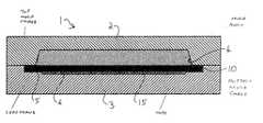
- FIG. 1is a cross-sectional view of a mold with a leadframe located in the mold after molding but before separation of the mold;
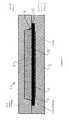
- FIG. 2is a plan view of a matrix leadframe with adhesive tape attached and one of the matrix blocks molded.
- FIG. 1shows a mold 1 which includes a first mold section 2 and a second mold section 3 .
- the first section of the mold 2includes a mold cavity 4 and the mold section 3 includes a first recess 6 and a second recess 5 .
- the first recess 6is located within the second recess 5 .
- FIG. 2is a plan view of a matrix leadframe 10 which includes four separate matrixes 11 of die attach pads 12 . Each die attach portion 12 can have a die (not shown) attached to it.
- an adhesive tape 15is applied to the underside of the leadframe 10 . That is the side opposite to the side on which the dies are to be attached. This is also shown in FIG. 1 .
- the adhesive tape 15is a pressure sensitive adhesive tape and is preferably a polyimide tape with silicon adhesive, such as Nitto Denko TRM-6250. After the tape is applied to the underside, dies are attached to each of the die attach pads 12 .
- the leadframe 10is forwarded to a conventional wire bonding machine (not shown).
- the wire bonding machinebonds wires between bond pads on each individual die attached to a pad 12 and corresponding leads on the leadframe 10 .
- the width of the tape 15is less than the width of the leadframe 10 .
- the thickness of the tape 15is also less than the thickness of the leadframe.
- the tapemay have a thickness of the order of 30 ⁇ m to to 35 ⁇ m.
- the first recess 6 in the second mold section 3preferably has a depth that is greater than the thickness of the tape 15 .
- the depth of the first recess 6is approximately 10% to 30% greater than the thickness of the tape, preferably, 20% to 30% greater and most preferably approximately 25% greater.
- the tape thicknessis approximately 30 ⁇ m to 35 ⁇ m
- the depthis 5 ⁇ m to 8 ⁇ m greater than the thickness of the tape and most preferably, the depth is approximately 5 ⁇ m greater than the thickness of the tape 15 .
- the adhesive tape usedis Nitto Denko TRM-6250
- the nominal tape thicknessis approximately 33 ⁇ m and the depth of the first recess 6 is approximately 38 ⁇ m.
- the leadframe 10is positioned in the second section 3 of the mold 1 such that the leadframe 10 is located in the second recess 5 .
- the tape 15locates within the first recess 6 .
- the inventorshave discovered that by providing a first recess 6 which is large enough to receive the tape 15 but too small to receive the leadframe, seepage of resin through to the underside of the leadframe 10 is reduced compared to conventional molds which do not have a first recess 6 .
- the performance of the inventionmay be further enhanced by preferably making the depth of the first recess 6 greater than the thickness of the tape 15 .
Landscapes
- Engineering & Computer Science (AREA)
- Manufacturing & Machinery (AREA)
- Mechanical Engineering (AREA)
- Physics & Mathematics (AREA)
- Condensed Matter Physics & Semiconductors (AREA)
- General Physics & Mathematics (AREA)
- Computer Hardware Design (AREA)
- Microelectronics & Electronic Packaging (AREA)
- Power Engineering (AREA)
- Lead Frames For Integrated Circuits (AREA)
- Encapsulation Of And Coatings For Semiconductor Or Solid State Devices (AREA)
- Moulds For Moulding Plastics Or The Like (AREA)
- Pens And Brushes (AREA)
- Materials For Medical Uses (AREA)
- Structures Or Materials For Encapsulating Or Coating Semiconductor Devices Or Solid State Devices (AREA)
- Apparatuses And Processes For Manufacturing Resistors (AREA)
Abstract
Description
The invention relates to a mold, and in particular, a mold for encapsulating an electronic device.
Conventionally, electronic devices, such as silicon chips (or dies) are assembled by attaching the die to a die attach pad of a leadframe, bonding gold wires between bond pads on the die to corresponding leads on the leadframe and then encapsulating the die, die pad and wires in a resin material so that only the external leads of the leadframe project from the encapsulated package.
In recent years, electronic devices have been developed in which only the side of the leadframe to which the die is attached and the wire bonds are encapsulated leaving the other side of the leadframe free of resin. Such one-sided encapsulated electronic devices are known by a number of different names, including molded leaded packages (MLP), micro leadframe packages (MLF) and quad flat non-leaded packages (QFN).
However, one of the problems with one-sided encapsulated devices is to ensure that during the molding process, the resin covers only one side of the leadframe and does not flow onto the other side of the leadframe. If the resin flows onto the other side of the leadframe, this can result in a defect on that particular device resulting in the device having to be rejected.
One solution to minimising this problem has been to apply adhesive tape to the opposite side of the leadframe from the die side and to then attach the dies and perform the wire bonding, followed by the molding process. The theory behind the use of the tape is that the presence of the adhesive tape on the other side of the leadframe prevents seepage of the resin during molding onto the portion of the leadframe that will become the external leads, thereby reducing the number of devices that have to be rejected.
However, in practice, it is found that resin still flows onto the other side of the leadframe despite the presence of the adhesive tape. This is especially the case with matrix leadframes where the outside row of chips is particularly prone to resin seepage. Hence, it is common practice not to attach dies to the outside row of die attach portions as the probability of resin seepage on the outer row is relatively high.
Therefore, the seepage of resin to the other side of the leadframe reduces the yield of usable chips from a given leadframe.
In accordance with a first aspect of the present invention, a mold for molding a one-sided encapsulated electronic device comprises a first mold section defining a mold cavity, and a second mold section including a first recessed portion adapted to receive a layer of material attached to a leadframe, but not the leadframe.
In accordance with a second aspect of the present invention, a method of encapsulating a one-sided electronic device comprises forming a leadframe assembly by attaching a layer of material to one side of a leadframe, attaching a die to a die attach portion on the other side of the leadframe, bonding wires between contact portions on the die and contact portions on the leadframe, inserting the leadframe assembly into a mold with the die in a mold cavity in a first section of the mold and the leadframe being located on a second section of the mold with the layer of material, but not the leadframe, being located in a first recessed portion of the second section of the mold.
Typically, at least one dimension of the layer of material is smaller than the corresponding dimension of the leadframe. Preferably, the width of the layer of material is smaller than the width of the leadframe.
Preferably, the depth of the first recessed portion is greater than the thickness of the layer of material. Typically, the first recessed portion has a depth which is approximately 10% to 30% greater than the layer of material, preferably 15% to 30% greater, more preferably, 20% to 30% greater and most preferably, approximately 25% greater than the thickness of the material.
Typically, the leadframe is located in a second recessed portion of the second section of the mold, and the first recessed portion is located within the second recessed portion.
Preferably, the layer of material is an adhesive film that is attached to the leadframe by the adhesive. Typically, the adhesive film may be in the form of an adhesive tape. Preferably, the adhesive tape is a polyimide tape with a silicon adhesive, such as Nitto Denko TRM-6250 adhesive tape.
An example of a mold in accordance with the invention will now be described with the accompanying drawings, in which:
FIG. 1 is a cross-sectional view of a mold with a leadframe located in the mold after molding but before separation of the mold; and
FIG. 2 is a plan view of a matrix leadframe with adhesive tape attached and one of the matrix blocks molded.
FIG. 1 shows a mold1 which includes afirst mold section 2 and asecond mold section 3. The first section of themold 2 includes amold cavity 4 and themold section 3 includes afirst recess 6 and asecond recess 5. Thefirst recess 6 is located within thesecond recess 5.
FIG. 2 is a plan view of amatrix leadframe 10 which includes four separate matrixes11 of dieattach pads 12. Each dieattach portion 12 can have a die (not shown) attached to it.
In use, anadhesive tape 15 is applied to the underside of theleadframe 10. That is the side opposite to the side on which the dies are to be attached. This is also shown in FIG.1. Typically, theadhesive tape 15 is a pressure sensitive adhesive tape and is preferably a polyimide tape with silicon adhesive, such as Nitto Denko TRM-6250. After the tape is applied to the underside, dies are attached to each of thedie attach pads 12.
After all the dies are attached to each of thedie attach pads 12 on each of the matrixes11, theleadframe 10 is forwarded to a conventional wire bonding machine (not shown). The wire bonding machine bonds wires between bond pads on each individual die attached to apad 12 and corresponding leads on theleadframe 10.
As shown in FIG. 2, the width of thetape 15 is less than the width of theleadframe 10. Typically, the thickness of thetape 15 is also less than the thickness of the leadframe. For example, the tape may have a thickness of the order of 30 μm to to 35 μm.
Thefirst recess 6 in thesecond mold section 3 preferably has a depth that is greater than the thickness of thetape 15. Typically, the depth of thefirst recess 6 is approximately 10% to 30% greater than the thickness of the tape, preferably, 20% to 30% greater and most preferably approximately 25% greater. For example if the tape thickness is approximately 30 μm to 35 μm, the depth is 5 μm to 8 μm greater than the thickness of the tape and most preferably, the depth is approximately 5 μm greater than the thickness of thetape 15. Typically, if the adhesive tape used is Nitto Denko TRM-6250, the nominal tape thickness is approximately 33 μm and the depth of thefirst recess 6 is approximately 38 μm.
As shown in FIG. 1, with theleadframe 10 inserted in the mold1, theleadframe 10 is positioned in thesecond section 3 of the mold1 such that theleadframe 10 is located in thesecond recess 5. Thetape 15 locates within thefirst recess 6.
Surprisingly, the inventors have discovered that by providing afirst recess 6 which is large enough to receive thetape 15 but too small to receive the leadframe, seepage of resin through to the underside of theleadframe 10 is reduced compared to conventional molds which do not have afirst recess 6. The performance of the invention may be further enhanced by preferably making the depth of thefirst recess 6 greater than the thickness of thetape 15.
Claims (18)
1. A mold for molding a one-sided encapsulated electronic device from a leadframe, a layer of material being attached to one side of the leadframe, the mold comprising:
a first mold section defining a mold cavity; and
a second mold section, the first and second mold sections configured to receive the leadframe therebetween for molding the one-sided encapsulated electronic device, the second mold section including a first recess sized to receive the entire layer of material attached to the leadframe and sized smaller than the leadframe so that the leadframe extends over the first recess without being received within the first recess.
2. A mold according toclaim 1 , wherein the second mold section includes a second recess sized to receive the entire leadframe, the first recess being located within the second recess.
3. A mold according toclaim 1 , wherein the layer of material has a thickness and the first recess has a depth that is greater than the thickness of the layer of material.
4. A mold according toclaim 3 , wherein the depth of the first recess is approximately 10% to 30% greater than the thickness of the layer of material.
5. A mold according toclaim 4 , wherein the depth of the first recess is approximately 15% to 30% greater than the thickness of the layer of material.
6. A mold according toclaim 5 , wherein the depth of the first recess is approximately 20% to 30% greater than the thickness of the layer of material.
7. A mold according toclaim 6 , wherein the depth of the first recess is approximately 25% greater than the thickness of the layer of material.
8. A method of forming a one-sided encapsulated electronic device, comprising:
forming a leadframe assembly by:
(i) attaching a layer of material to one side of a leadframe, the leadframe including contact portions,
(ii) attaching a die to a die attach portion of the leadframe on another side of the leadframe, the die including contact portions, and
(iii) bonding wires between the contact portions of the die and the contact portions of the leadframe;
inserting the leadframe assembly into a mold, the mold including a first mold section defining a mold cavity, and a second mold section including a first recess sized to receive the entire layer of material attached to the leadframe and sized smaller than the leadframe so that the leadframe extends over the first recess without being received within the first recess; and
inserting a molding material into the mold cavity of the first mold section to form the one-sided encapsulated electronic device.
9. A method according toclaim 8 , wherein the layer of material has a thickness and the first recess has a depth that is greater than the thickness of the layer of material.
10. A method according toclaim 9 , wherein the depth of the first recess is approximately 10% to 30% greater than the thickness of the layer of material.
11. A method according toclaim 10 , wherein the depth of the first recess is approximately 15% to 30% greater than the thickness of the layer of material.
12. A method according toclaim 11 , wherein the depth of the first recess is approximately 20% to 30% greater than the thickness of the layer of material.
13. A method according toclaim 12 , wherein the depth of the first recess is approximately 25% greater than the thickness of the layer of material.
14. A method according toclaim 8 , wherein a thickness of the layer of material is from 15 μm to 60 μm.
15. A method according toclaim 14 , wherein the thickness of the layer of material is from 30 μm to 40 μm.
16. A method according toclaim 8 , wherein the second mold section of the mold includes a second recess sized to receive the leadframe, the first recess of the second mold section being located with the second recess of the second mold section, the leadframe assembly being inserted into the mold such that the leadframe is located entirely within the second recess.
17. A method according toclaim 8 , wherein the layer of material is an adhesive film having an adhesive, the layer of material being attached to the leadframe via the adhesive.
18. A method according toclaim 17 , wherein the adhesive film is an adhesive tape.
Applications Claiming Priority (1)
| Application Number | Priority Date | Filing Date | Title |
|---|---|---|---|
| PCT/SG2000/000140WO2002020236A2 (en) | 2000-09-08 | 2000-09-08 | A mold |
Publications (1)
| Publication Number | Publication Date |
|---|---|
| US6770163B1true US6770163B1 (en) | 2004-08-03 |
Family
ID=20428860
Family Applications (1)
| Application Number | Title | Priority Date | Filing Date |
|---|---|---|---|
| US10/129,258Expired - LifetimeUS6770163B1 (en) | 2000-09-08 | 2000-09-08 | Mold and method for encapsulation of electronic device |
Country Status (7)
| Country | Link |
|---|---|
| US (1) | US6770163B1 (en) |
| EP (1) | EP1315605B1 (en) |
| CN (1) | CN1387678A (en) |
| AT (1) | ATE263431T1 (en) |
| AU (1) | AU2000275687A1 (en) |
| DE (1) | DE60009579D1 (en) |
| WO (1) | WO2002020236A2 (en) |
Cited By (50)
| Publication number | Priority date | Publication date | Assignee | Title |
|---|---|---|---|---|
| US20040159928A1 (en)* | 2002-11-22 | 2004-08-19 | Infineon Technologies Ag | Supporting structure for a chip and method for producing the same |
| US20050253208A1 (en)* | 2004-05-13 | 2005-11-17 | Mitsubishi Denki Kabushiki Kaisha | Semiconductor micro device |
| US20070013066A1 (en)* | 2005-07-15 | 2007-01-18 | Siliconware Precision Industries Co., Ltd. | Semiconductor package and fabrication method thereof |
| WO2008079072A1 (en) | 2006-12-22 | 2008-07-03 | Kiram Ab | Method for recovering a low sodium content lignin fuel from black liquor |
| US20080237818A1 (en)* | 2007-03-29 | 2008-10-02 | Engel Raymond W | Methods and apparatus for multi-stage molding of integrated circuit package |
| US20090108424A1 (en)* | 2007-10-31 | 2009-04-30 | Chipmos Technologies Inc. | Leadframe for leadless package |
| US20100019332A1 (en)* | 2008-07-24 | 2010-01-28 | Taylor William P | Methods and apparatus for integrated circuit having on chip capacitor with eddy current reductions |
| US20100188078A1 (en)* | 2009-01-28 | 2010-07-29 | Andrea Foletto | Magnetic sensor with concentrator for increased sensing range |
| US20110133732A1 (en)* | 2009-12-03 | 2011-06-09 | Allegro Microsystems, Inc. | Methods and apparatus for enhanced frequency response of magnetic sensors |
| US8461677B2 (en) | 2008-12-05 | 2013-06-11 | Allegro Microsystems, Llc | Magnetic field sensors and methods for fabricating the magnetic field sensors |
| US8629539B2 (en) | 2012-01-16 | 2014-01-14 | Allegro Microsystems, Llc | Methods and apparatus for magnetic sensor having non-conductive die paddle |
| US9228860B2 (en) | 2006-07-14 | 2016-01-05 | Allegro Microsystems, Llc | Sensor and method of providing a sensor |
| WO2016043993A1 (en)* | 2014-09-15 | 2016-03-24 | Micron Technology, Inc. | Methods of protecting peripheries of in-process semiconductor wafers and related in-process wafers and systems |
| US9411025B2 (en) | 2013-04-26 | 2016-08-09 | Allegro Microsystems, Llc | Integrated circuit package having a split lead frame and a magnet |
| US9494660B2 (en) | 2012-03-20 | 2016-11-15 | Allegro Microsystems, Llc | Integrated circuit package having a split lead frame |
| US9666788B2 (en) | 2012-03-20 | 2017-05-30 | Allegro Microsystems, Llc | Integrated circuit package having a split lead frame |
| US9720054B2 (en) | 2014-10-31 | 2017-08-01 | Allegro Microsystems, Llc | Magnetic field sensor and electronic circuit that pass amplifier current through a magnetoresistance element |
| US9719806B2 (en) | 2014-10-31 | 2017-08-01 | Allegro Microsystems, Llc | Magnetic field sensor for sensing a movement of a ferromagnetic target object |
| US9812588B2 (en) | 2012-03-20 | 2017-11-07 | Allegro Microsystems, Llc | Magnetic field sensor integrated circuit with integral ferromagnetic material |
| US9810519B2 (en) | 2013-07-19 | 2017-11-07 | Allegro Microsystems, Llc | Arrangements for magnetic field sensors that act as tooth detectors |
| US9817078B2 (en) | 2012-05-10 | 2017-11-14 | Allegro Microsystems Llc | Methods and apparatus for magnetic sensor having integrated coil |
| US9823092B2 (en) | 2014-10-31 | 2017-11-21 | Allegro Microsystems, Llc | Magnetic field sensor providing a movement detector |
| US9823090B2 (en) | 2014-10-31 | 2017-11-21 | Allegro Microsystems, Llc | Magnetic field sensor for sensing a movement of a target object |
| US10012518B2 (en) | 2016-06-08 | 2018-07-03 | Allegro Microsystems, Llc | Magnetic field sensor for sensing a proximity of an object |
| US10041810B2 (en) | 2016-06-08 | 2018-08-07 | Allegro Microsystems, Llc | Arrangements for magnetic field sensors that act as movement detectors |
| US10145908B2 (en) | 2013-07-19 | 2018-12-04 | Allegro Microsystems, Llc | Method and apparatus for magnetic sensor producing a changing magnetic field |
| US10215550B2 (en) | 2012-05-01 | 2019-02-26 | Allegro Microsystems, Llc | Methods and apparatus for magnetic sensors having highly uniform magnetic fields |
| US10234513B2 (en) | 2012-03-20 | 2019-03-19 | Allegro Microsystems, Llc | Magnetic field sensor integrated circuit with integral ferromagnetic material |
| US10260905B2 (en) | 2016-06-08 | 2019-04-16 | Allegro Microsystems, Llc | Arrangements for magnetic field sensors to cancel offset variations |
| US10310028B2 (en) | 2017-05-26 | 2019-06-04 | Allegro Microsystems, Llc | Coil actuated pressure sensor |
| US10324141B2 (en) | 2017-05-26 | 2019-06-18 | Allegro Microsystems, Llc | Packages for coil actuated position sensors |
| US10495699B2 (en) | 2013-07-19 | 2019-12-03 | Allegro Microsystems, Llc | Methods and apparatus for magnetic sensor having an integrated coil or magnet to detect a non-ferromagnetic target |
| US10641842B2 (en) | 2017-05-26 | 2020-05-05 | Allegro Microsystems, Llc | Targets for coil actuated position sensors |
| US10712403B2 (en) | 2014-10-31 | 2020-07-14 | Allegro Microsystems, Llc | Magnetic field sensor and electronic circuit that pass amplifier current through a magnetoresistance element |
| US10725100B2 (en) | 2013-03-15 | 2020-07-28 | Allegro Microsystems, Llc | Methods and apparatus for magnetic sensor having an externally accessible coil |
| US10823586B2 (en) | 2018-12-26 | 2020-11-03 | Allegro Microsystems, Llc | Magnetic field sensor having unequally spaced magnetic field sensing elements |
| US10837943B2 (en) | 2017-05-26 | 2020-11-17 | Allegro Microsystems, Llc | Magnetic field sensor with error calculation |
| US10866117B2 (en) | 2018-03-01 | 2020-12-15 | Allegro Microsystems, Llc | Magnetic field influence during rotation movement of magnetic target |
| US10921391B2 (en) | 2018-08-06 | 2021-02-16 | Allegro Microsystems, Llc | Magnetic field sensor with spacer |
| US10955306B2 (en) | 2019-04-22 | 2021-03-23 | Allegro Microsystems, Llc | Coil actuated pressure sensor and deformable substrate |
| US10991644B2 (en) | 2019-08-22 | 2021-04-27 | Allegro Microsystems, Llc | Integrated circuit package having a low profile |
| US10996289B2 (en) | 2017-05-26 | 2021-05-04 | Allegro Microsystems, Llc | Coil actuated position sensor with reflected magnetic field |
| US11061084B2 (en) | 2019-03-07 | 2021-07-13 | Allegro Microsystems, Llc | Coil actuated pressure sensor and deflectable substrate |
| US11237020B2 (en) | 2019-11-14 | 2022-02-01 | Allegro Microsystems, Llc | Magnetic field sensor having two rows of magnetic field sensing elements for measuring an angle of rotation of a magnet |
| US11255700B2 (en) | 2018-08-06 | 2022-02-22 | Allegro Microsystems, Llc | Magnetic field sensor |
| US11262422B2 (en) | 2020-05-08 | 2022-03-01 | Allegro Microsystems, Llc | Stray-field-immune coil-activated position sensor |
| US11280637B2 (en) | 2019-11-14 | 2022-03-22 | Allegro Microsystems, Llc | High performance magnetic angle sensor |
| US11428755B2 (en) | 2017-05-26 | 2022-08-30 | Allegro Microsystems, Llc | Coil actuated sensor with sensitivity detection |
| US11493361B2 (en) | 2021-02-26 | 2022-11-08 | Allegro Microsystems, Llc | Stray field immune coil-activated sensor |
| US11578997B1 (en) | 2021-08-24 | 2023-02-14 | Allegro Microsystems, Llc | Angle sensor using eddy currents |
Families Citing this family (1)
| Publication number | Priority date | Publication date | Assignee | Title |
|---|---|---|---|---|
| CN102744176B (en)* | 2012-07-07 | 2017-04-26 | 上海鼎虹电子有限公司 | Cleaning agent coating bracket in encapsulation of electronic elements |
Citations (7)
| Publication number | Priority date | Publication date | Assignee | Title |
|---|---|---|---|---|
| US4822550A (en)* | 1986-04-17 | 1989-04-18 | Citizen Watch Co., Ltd. | Method of molding a protective cover on a pin grid array |
| US4890152A (en)* | 1986-02-14 | 1989-12-26 | Matsushita Electric Works, Ltd. | Plastic molded chip carrier package and method of fabricating the same |
| US5218759A (en)* | 1991-03-18 | 1993-06-15 | Motorola, Inc. | Method of making a transfer molded semiconductor device |
| US5656549A (en)* | 1996-08-19 | 1997-08-12 | Motorola, Inc. | Method of packaging a semiconductor device |
| US5958466A (en)* | 1997-06-04 | 1999-09-28 | Ipac, Inc. | Pressure-plate-operative system for one-side injection molding of substrate-mounted integrated circuits |
| US6126885A (en)* | 1997-06-27 | 2000-10-03 | Matsushita Electronics Corporation | Method for manufacturing resin-molded semiconductor device |
| US6403387B1 (en)* | 1997-02-25 | 2002-06-11 | Micron Technology | Method and apparatus for transfer molding encapsulation of a semiconductor die with attached heat sink |
Family Cites Families (3)
| Publication number | Priority date | Publication date | Assignee | Title |
|---|---|---|---|---|
| IT1252575B (en)* | 1991-12-20 | 1995-06-19 | Sgs Thomson Microelectronics | MOLD AND PROCESS FOR THE MANUFACTURE OF SEMICONDUCTOR PLASTIC DEVICES, WITH VISIBLE METALLIC DISSIPATOR FOR WELDING CONTROL |
| US5923959A (en)* | 1997-07-23 | 1999-07-13 | Micron Technology, Inc. | Ball grid array (BGA) encapsulation mold |
| JP3897478B2 (en)* | 1999-03-31 | 2007-03-22 | 松下電器産業株式会社 | Apparatus for manufacturing resin-encapsulated semiconductor device and method for manufacturing the same |
- 2000
- 2000-09-08ATAT00964866Tpatent/ATE263431T1/ennot_activeIP Right Cessation
- 2000-09-08USUS10/129,258patent/US6770163B1/ennot_activeExpired - Lifetime
- 2000-09-08WOPCT/SG2000/000140patent/WO2002020236A2/enactiveIP Right Grant
- 2000-09-08DEDE60009579Tpatent/DE60009579D1/ennot_activeExpired - Lifetime
- 2000-09-08EPEP00964866Apatent/EP1315605B1/ennot_activeExpired - Lifetime
- 2000-09-08AUAU2000275687Apatent/AU2000275687A1/ennot_activeAbandoned
- 2000-09-08CNCN00815318Apatent/CN1387678A/enactivePending
Patent Citations (9)
| Publication number | Priority date | Publication date | Assignee | Title |
|---|---|---|---|---|
| US4890152A (en)* | 1986-02-14 | 1989-12-26 | Matsushita Electric Works, Ltd. | Plastic molded chip carrier package and method of fabricating the same |
| US4822550A (en)* | 1986-04-17 | 1989-04-18 | Citizen Watch Co., Ltd. | Method of molding a protective cover on a pin grid array |
| US5218759A (en)* | 1991-03-18 | 1993-06-15 | Motorola, Inc. | Method of making a transfer molded semiconductor device |
| US5656549A (en)* | 1996-08-19 | 1997-08-12 | Motorola, Inc. | Method of packaging a semiconductor device |
| US6403387B1 (en)* | 1997-02-25 | 2002-06-11 | Micron Technology | Method and apparatus for transfer molding encapsulation of a semiconductor die with attached heat sink |
| US6583504B2 (en)* | 1997-02-25 | 2003-06-24 | Micron Technology, Inc. | Semiconductor die with attached heat sink and transfer mold |
| US5958466A (en)* | 1997-06-04 | 1999-09-28 | Ipac, Inc. | Pressure-plate-operative system for one-side injection molding of substrate-mounted integrated circuits |
| US6126885A (en)* | 1997-06-27 | 2000-10-03 | Matsushita Electronics Corporation | Method for manufacturing resin-molded semiconductor device |
| US6258314B1 (en)* | 1997-06-27 | 2001-07-10 | Matsushita Electronics Corporation | Method for manufacturing resin-molded semiconductor device |
Cited By (80)
| Publication number | Priority date | Publication date | Assignee | Title |
|---|---|---|---|---|
| US20040159928A1 (en)* | 2002-11-22 | 2004-08-19 | Infineon Technologies Ag | Supporting structure for a chip and method for producing the same |
| US20050253208A1 (en)* | 2004-05-13 | 2005-11-17 | Mitsubishi Denki Kabushiki Kaisha | Semiconductor micro device |
| US20070013066A1 (en)* | 2005-07-15 | 2007-01-18 | Siliconware Precision Industries Co., Ltd. | Semiconductor package and fabrication method thereof |
| US9228860B2 (en) | 2006-07-14 | 2016-01-05 | Allegro Microsystems, Llc | Sensor and method of providing a sensor |
| WO2008079072A1 (en) | 2006-12-22 | 2008-07-03 | Kiram Ab | Method for recovering a low sodium content lignin fuel from black liquor |
| US20100330708A1 (en)* | 2007-03-29 | 2010-12-30 | Allegro Microsystems, Inc. | Methods for multi-stage molding of integrated circuit package |
| US7816772B2 (en) | 2007-03-29 | 2010-10-19 | Allegro Microsystems, Inc. | Methods and apparatus for multi-stage molding of integrated circuit package |
| US20080237818A1 (en)* | 2007-03-29 | 2008-10-02 | Engel Raymond W | Methods and apparatus for multi-stage molding of integrated circuit package |
| US8143169B2 (en) | 2007-03-29 | 2012-03-27 | Allegro Microsystems, Inc. | Methods for multi-stage molding of integrated circuit package |
| US20090108424A1 (en)* | 2007-10-31 | 2009-04-30 | Chipmos Technologies Inc. | Leadframe for leadless package |
| US20100019332A1 (en)* | 2008-07-24 | 2010-01-28 | Taylor William P | Methods and apparatus for integrated circuit having on chip capacitor with eddy current reductions |
| US8093670B2 (en) | 2008-07-24 | 2012-01-10 | Allegro Microsystems, Inc. | Methods and apparatus for integrated circuit having on chip capacitor with eddy current reductions |
| US8461677B2 (en) | 2008-12-05 | 2013-06-11 | Allegro Microsystems, Llc | Magnetic field sensors and methods for fabricating the magnetic field sensors |
| US8486755B2 (en) | 2008-12-05 | 2013-07-16 | Allegro Microsystems, Llc | Magnetic field sensors and methods for fabricating the magnetic field sensors |
| US20100188078A1 (en)* | 2009-01-28 | 2010-07-29 | Andrea Foletto | Magnetic sensor with concentrator for increased sensing range |
| US20110133732A1 (en)* | 2009-12-03 | 2011-06-09 | Allegro Microsystems, Inc. | Methods and apparatus for enhanced frequency response of magnetic sensors |
| US8629539B2 (en) | 2012-01-16 | 2014-01-14 | Allegro Microsystems, Llc | Methods and apparatus for magnetic sensor having non-conductive die paddle |
| US10333055B2 (en) | 2012-01-16 | 2019-06-25 | Allegro Microsystems, Llc | Methods for magnetic sensor having non-conductive die paddle |
| US9299915B2 (en) | 2012-01-16 | 2016-03-29 | Allegro Microsystems, Llc | Methods and apparatus for magnetic sensor having non-conductive die paddle |
| US9620705B2 (en) | 2012-01-16 | 2017-04-11 | Allegro Microsystems, Llc | Methods and apparatus for magnetic sensor having non-conductive die paddle |
| US11961920B2 (en) | 2012-03-20 | 2024-04-16 | Allegro Microsystems, Llc | Integrated circuit package with magnet having a channel |
| US11677032B2 (en) | 2012-03-20 | 2023-06-13 | Allegro Microsystems, Llc | Sensor integrated circuit with integrated coil and element in central region of mold material |
| US10234513B2 (en) | 2012-03-20 | 2019-03-19 | Allegro Microsystems, Llc | Magnetic field sensor integrated circuit with integral ferromagnetic material |
| US9666788B2 (en) | 2012-03-20 | 2017-05-30 | Allegro Microsystems, Llc | Integrated circuit package having a split lead frame |
| US10916665B2 (en) | 2012-03-20 | 2021-02-09 | Allegro Microsystems, Llc | Magnetic field sensor integrated circuit with an integrated coil |
| US11444209B2 (en) | 2012-03-20 | 2022-09-13 | Allegro Microsystems, Llc | Magnetic field sensor integrated circuit with an integrated coil enclosed with a semiconductor die by a mold material |
| US9812588B2 (en) | 2012-03-20 | 2017-11-07 | Allegro Microsystems, Llc | Magnetic field sensor integrated circuit with integral ferromagnetic material |
| US10230006B2 (en) | 2012-03-20 | 2019-03-12 | Allegro Microsystems, Llc | Magnetic field sensor integrated circuit with an electromagnetic suppressor |
| US11828819B2 (en) | 2012-03-20 | 2023-11-28 | Allegro Microsystems, Llc | Magnetic field sensor integrated circuit with integral ferromagnetic material |
| US9494660B2 (en) | 2012-03-20 | 2016-11-15 | Allegro Microsystems, Llc | Integrated circuit package having a split lead frame |
| US10215550B2 (en) | 2012-05-01 | 2019-02-26 | Allegro Microsystems, Llc | Methods and apparatus for magnetic sensors having highly uniform magnetic fields |
| US11680996B2 (en) | 2012-05-10 | 2023-06-20 | Allegro Microsystems, Llc | Methods and apparatus for magnetic sensor having integrated coil |
| US9817078B2 (en) | 2012-05-10 | 2017-11-14 | Allegro Microsystems Llc | Methods and apparatus for magnetic sensor having integrated coil |
| US10725100B2 (en) | 2013-03-15 | 2020-07-28 | Allegro Microsystems, Llc | Methods and apparatus for magnetic sensor having an externally accessible coil |
| US9411025B2 (en) | 2013-04-26 | 2016-08-09 | Allegro Microsystems, Llc | Integrated circuit package having a split lead frame and a magnet |
| US10670672B2 (en) | 2013-07-19 | 2020-06-02 | Allegro Microsystems, Llc | Method and apparatus for magnetic sensor producing a changing magnetic field |
| US10145908B2 (en) | 2013-07-19 | 2018-12-04 | Allegro Microsystems, Llc | Method and apparatus for magnetic sensor producing a changing magnetic field |
| US10254103B2 (en) | 2013-07-19 | 2019-04-09 | Allegro Microsystems, Llc | Arrangements for magnetic field sensors that act as tooth detectors |
| US11313924B2 (en) | 2013-07-19 | 2022-04-26 | Allegro Microsystems, Llc | Method and apparatus for magnetic sensor producing a changing magnetic field |
| US12061246B2 (en) | 2013-07-19 | 2024-08-13 | Allegro Microsystems, Llc | Method and apparatus for magnetic sensor producing a changing magnetic field |
| US10495699B2 (en) | 2013-07-19 | 2019-12-03 | Allegro Microsystems, Llc | Methods and apparatus for magnetic sensor having an integrated coil or magnet to detect a non-ferromagnetic target |
| US9810519B2 (en) | 2013-07-19 | 2017-11-07 | Allegro Microsystems, Llc | Arrangements for magnetic field sensors that act as tooth detectors |
| US9337064B2 (en) | 2014-09-15 | 2016-05-10 | Micron Technology, Inc. | Methods of protecting peripheries of in-process semiconductor wafers and related in-process wafers and systems |
| WO2016043993A1 (en)* | 2014-09-15 | 2016-03-24 | Micron Technology, Inc. | Methods of protecting peripheries of in-process semiconductor wafers and related in-process wafers and systems |
| US10712403B2 (en) | 2014-10-31 | 2020-07-14 | Allegro Microsystems, Llc | Magnetic field sensor and electronic circuit that pass amplifier current through a magnetoresistance element |
| US9823090B2 (en) | 2014-10-31 | 2017-11-21 | Allegro Microsystems, Llc | Magnetic field sensor for sensing a movement of a target object |
| US10753769B2 (en) | 2014-10-31 | 2020-08-25 | Allegro Microsystems, Llc | Magnetic field sensor providing a movement detector |
| US10753768B2 (en) | 2014-10-31 | 2020-08-25 | Allegro Microsystems, Llc | Magnetic field sensor providing a movement detector |
| US9823092B2 (en) | 2014-10-31 | 2017-11-21 | Allegro Microsystems, Llc | Magnetic field sensor providing a movement detector |
| US11307054B2 (en) | 2014-10-31 | 2022-04-19 | Allegro Microsystems, Llc | Magnetic field sensor providing a movement detector |
| US9719806B2 (en) | 2014-10-31 | 2017-08-01 | Allegro Microsystems, Llc | Magnetic field sensor for sensing a movement of a ferromagnetic target object |
| US9720054B2 (en) | 2014-10-31 | 2017-08-01 | Allegro Microsystems, Llc | Magnetic field sensor and electronic circuit that pass amplifier current through a magnetoresistance element |
| US10012518B2 (en) | 2016-06-08 | 2018-07-03 | Allegro Microsystems, Llc | Magnetic field sensor for sensing a proximity of an object |
| US10041810B2 (en) | 2016-06-08 | 2018-08-07 | Allegro Microsystems, Llc | Arrangements for magnetic field sensors that act as movement detectors |
| US10837800B2 (en) | 2016-06-08 | 2020-11-17 | Allegro Microsystems, Llc | Arrangements for magnetic field sensors that act as movement detectors |
| US10260905B2 (en) | 2016-06-08 | 2019-04-16 | Allegro Microsystems, Llc | Arrangements for magnetic field sensors to cancel offset variations |
| US10310028B2 (en) | 2017-05-26 | 2019-06-04 | Allegro Microsystems, Llc | Coil actuated pressure sensor |
| US11320496B2 (en) | 2017-05-26 | 2022-05-03 | Allegro Microsystems, Llc | Targets for coil actuated position sensors |
| US10996289B2 (en) | 2017-05-26 | 2021-05-04 | Allegro Microsystems, Llc | Coil actuated position sensor with reflected magnetic field |
| US10324141B2 (en) | 2017-05-26 | 2019-06-18 | Allegro Microsystems, Llc | Packages for coil actuated position sensors |
| US11073573B2 (en) | 2017-05-26 | 2021-07-27 | Allegro Microsystems, Llc | Packages for coil actuated position sensors |
| US10641842B2 (en) | 2017-05-26 | 2020-05-05 | Allegro Microsystems, Llc | Targets for coil actuated position sensors |
| US10649042B2 (en) | 2017-05-26 | 2020-05-12 | Allegro Microsystems, Llc | Packages for coil actuated position sensors |
| US11768256B2 (en) | 2017-05-26 | 2023-09-26 | Allegro Microsystems, Llc | Coil actuated sensor with sensitivity detection |
| US10837943B2 (en) | 2017-05-26 | 2020-11-17 | Allegro Microsystems, Llc | Magnetic field sensor with error calculation |
| US11428755B2 (en) | 2017-05-26 | 2022-08-30 | Allegro Microsystems, Llc | Coil actuated sensor with sensitivity detection |
| US10866117B2 (en) | 2018-03-01 | 2020-12-15 | Allegro Microsystems, Llc | Magnetic field influence during rotation movement of magnetic target |
| US11313700B2 (en) | 2018-03-01 | 2022-04-26 | Allegro Microsystems, Llc | Magnetic field influence during rotation movement of magnetic target |
| US10921391B2 (en) | 2018-08-06 | 2021-02-16 | Allegro Microsystems, Llc | Magnetic field sensor with spacer |
| US11686599B2 (en) | 2018-08-06 | 2023-06-27 | Allegro Microsystems, Llc | Magnetic field sensor |
| US11255700B2 (en) | 2018-08-06 | 2022-02-22 | Allegro Microsystems, Llc | Magnetic field sensor |
| US10823586B2 (en) | 2018-12-26 | 2020-11-03 | Allegro Microsystems, Llc | Magnetic field sensor having unequally spaced magnetic field sensing elements |
| US11061084B2 (en) | 2019-03-07 | 2021-07-13 | Allegro Microsystems, Llc | Coil actuated pressure sensor and deflectable substrate |
| US10955306B2 (en) | 2019-04-22 | 2021-03-23 | Allegro Microsystems, Llc | Coil actuated pressure sensor and deformable substrate |
| US10991644B2 (en) | 2019-08-22 | 2021-04-27 | Allegro Microsystems, Llc | Integrated circuit package having a low profile |
| US11280637B2 (en) | 2019-11-14 | 2022-03-22 | Allegro Microsystems, Llc | High performance magnetic angle sensor |
| US11237020B2 (en) | 2019-11-14 | 2022-02-01 | Allegro Microsystems, Llc | Magnetic field sensor having two rows of magnetic field sensing elements for measuring an angle of rotation of a magnet |
| US11262422B2 (en) | 2020-05-08 | 2022-03-01 | Allegro Microsystems, Llc | Stray-field-immune coil-activated position sensor |
| US11493361B2 (en) | 2021-02-26 | 2022-11-08 | Allegro Microsystems, Llc | Stray field immune coil-activated sensor |
| US11578997B1 (en) | 2021-08-24 | 2023-02-14 | Allegro Microsystems, Llc | Angle sensor using eddy currents |
Also Published As
| Publication number | Publication date |
|---|---|
| CN1387678A (en) | 2002-12-25 |
| EP1315605A2 (en) | 2003-06-04 |
| WO2002020236A2 (en) | 2002-03-14 |
| AU2000275687A1 (en) | 2002-03-22 |
| DE60009579D1 (en) | 2004-05-06 |
| WO2002020236A3 (en) | 2002-05-23 |
| EP1315605B1 (en) | 2004-03-31 |
| ATE263431T1 (en) | 2004-04-15 |
Similar Documents
| Publication | Publication Date | Title |
|---|---|---|
| US6770163B1 (en) | Mold and method for encapsulation of electronic device | |
| US5767566A (en) | Plastic mold type semiconductor device | |
| US8836101B2 (en) | Multi-chip semiconductor packages and assembly thereof | |
| US6482675B2 (en) | Substrate strip for use in packaging semiconductor chips and method for making the substrate strip | |
| EP1335427B1 (en) | Resin-moulded semiconductor device | |
| US6603196B2 (en) | Leadframe-based semiconductor package for multi-media card | |
| US6864423B2 (en) | Bump chip lead frame and package | |
| KR20010039537A (en) | semiconductor package and its manufacturing method | |
| JPH09199637A (en) | Resin-sealed semiconductor device and method of manufacturing the same | |
| KR100586699B1 (en) | Semiconductor chip package and its manufacturing method | |
| US6979886B2 (en) | Short-prevented lead frame and method for fabricating semiconductor package with the same | |
| US6882048B2 (en) | Lead frame and semiconductor package having a groove formed in the respective terminals for limiting a plating area | |
| US6645792B2 (en) | Lead frame and method for fabricating resin-encapsulated semiconductor device | |
| US20020048851A1 (en) | Process for making a semiconductor package | |
| JPH05291459A (en) | Semiconductor device and manufacture thereof | |
| US6687983B2 (en) | Non leadframe clamping for matrix leadless leadframe package molding | |
| US7803667B2 (en) | Manufacturing process for a quad flat non-leaded chip package structure | |
| JP4475785B2 (en) | Manufacturing method of resin-encapsulated semiconductor device | |
| US8273445B2 (en) | Reinforced assembly carrier | |
| JPH08222676A (en) | Lead frame and manufacture of resin sealed semiconductor device employing it | |
| JPH11220087A (en) | Lead frame, semiconductor device using the same, and method of manufacturing the same | |
| JP2885708B2 (en) | Resin sealing mold and method of manufacturing semiconductor device | |
| JPH07105408B2 (en) | Method for manufacturing resin-encapsulated semiconductor device and molding die | |
| KR100753406B1 (en) | Semiconductor Package | |
| JPH07130782A (en) | Manufacture of package-type semiconductor device having heatsink |
Legal Events
| Date | Code | Title | Description |
|---|---|---|---|
| AS | Assignment | Owner name:ASM TECHNOLOGY SINGAPORE PTE LTD, SINGAPORE Free format text:ASSIGNMENT OF ASSIGNORS INTEREST;ASSIGNORS:KUAH, TENG HOCK;HO, SHU CHUEN;VATH, CHARLES JOSEPH III;AND OTHERS;REEL/FRAME:013039/0113;SIGNING DATES FROM 20020305 TO 20020404 | |
| STCF | Information on status: patent grant | Free format text:PATENTED CASE | |
| FPAY | Fee payment | Year of fee payment:4 | |
| FPAY | Fee payment | Year of fee payment:8 | |
| FPAY | Fee payment | Year of fee payment:12 |