US6768692B2 - Multiple subarray DRAM having a single shared sense amplifier - Google Patents
Multiple subarray DRAM having a single shared sense amplifierDownload PDFInfo
- Publication number
- US6768692B2 US6768692B2US10/207,366US20736602AUS6768692B2US 6768692 B2US6768692 B2US 6768692B2US 20736602 AUS20736602 AUS 20736602AUS 6768692 B2US6768692 B2US 6768692B2
- Authority
- US
- United States
- Prior art keywords
- bit
- lines
- dram
- global
- write
- Prior art date
- Legal status (The legal status is an assumption and is not a legal conclusion. Google has not performed a legal analysis and makes no representation as to the accuracy of the status listed.)
- Expired - Lifetime, expires
Links
- 238000003491arrayMethods0.000claimsabstractdescription27
- 230000015654memoryEffects0.000claimsabstractdescription20
- 238000000034methodMethods0.000claimsabstractdescription12
- 239000000872bufferSubstances0.000claimsdescription39
- 230000004913activationEffects0.000claimsdescription2
- 238000007599dischargingMethods0.000description4
- 230000008520organizationEffects0.000description2
- 230000000295complement effectEffects0.000description1
- 230000008878couplingEffects0.000description1
- 238000010168coupling processMethods0.000description1
- 238000005859coupling reactionMethods0.000description1
- 238000010586diagramMethods0.000description1
- 238000005516engineering processMethods0.000description1
- 230000006872improvementEffects0.000description1
- 238000012986modificationMethods0.000description1
- 230000004048modificationEffects0.000description1
- 230000002093peripheral effectEffects0.000description1
- 239000004065semiconductorSubstances0.000description1
Images


Classifications
- G—PHYSICS
- G11—INFORMATION STORAGE
- G11C—STATIC STORES
- G11C7/00—Arrangements for writing information into, or reading information out from, a digital store
- G11C7/06—Sense amplifiers; Associated circuits, e.g. timing or triggering circuits
- G11C7/065—Differential amplifiers of latching type
- G—PHYSICS
- G11—INFORMATION STORAGE
- G11C—STATIC STORES
- G11C11/00—Digital stores characterised by the use of particular electric or magnetic storage elements; Storage elements therefor
- G11C11/21—Digital stores characterised by the use of particular electric or magnetic storage elements; Storage elements therefor using electric elements
- G11C11/34—Digital stores characterised by the use of particular electric or magnetic storage elements; Storage elements therefor using electric elements using semiconductor devices
- G11C11/40—Digital stores characterised by the use of particular electric or magnetic storage elements; Storage elements therefor using electric elements using semiconductor devices using transistors
- G11C11/401—Digital stores characterised by the use of particular electric or magnetic storage elements; Storage elements therefor using electric elements using semiconductor devices using transistors forming cells needing refreshing or charge regeneration, i.e. dynamic cells
- G11C11/4063—Auxiliary circuits, e.g. for addressing, decoding, driving, writing, sensing or timing
- G11C11/407—Auxiliary circuits, e.g. for addressing, decoding, driving, writing, sensing or timing for memory cells of the field-effect type
- G11C11/409—Read-write [R-W] circuits
- G11C11/4091—Sense or sense/refresh amplifiers, or associated sense circuitry, e.g. for coupled bit-line precharging, equalising or isolating
- G—PHYSICS
- G11—INFORMATION STORAGE
- G11C—STATIC STORES
- G11C11/00—Digital stores characterised by the use of particular electric or magnetic storage elements; Storage elements therefor
- G11C11/21—Digital stores characterised by the use of particular electric or magnetic storage elements; Storage elements therefor using electric elements
- G11C11/34—Digital stores characterised by the use of particular electric or magnetic storage elements; Storage elements therefor using electric elements using semiconductor devices
- G11C11/40—Digital stores characterised by the use of particular electric or magnetic storage elements; Storage elements therefor using electric elements using semiconductor devices using transistors
- G11C11/401—Digital stores characterised by the use of particular electric or magnetic storage elements; Storage elements therefor using electric elements using semiconductor devices using transistors forming cells needing refreshing or charge regeneration, i.e. dynamic cells
- G11C11/4063—Auxiliary circuits, e.g. for addressing, decoding, driving, writing, sensing or timing
- G11C11/407—Auxiliary circuits, e.g. for addressing, decoding, driving, writing, sensing or timing for memory cells of the field-effect type
- G11C11/409—Read-write [R-W] circuits
- G11C11/4097—Bit-line organisation, e.g. bit-line layout, folded bit lines
- G—PHYSICS
- G11—INFORMATION STORAGE
- G11C—STATIC STORES
- G11C7/00—Arrangements for writing information into, or reading information out from, a digital store
- G11C7/18—Bit line organisation; Bit line lay-out
Definitions
- This inventionrelates to DRAMs having a new sensing architecture.
- the conventional two stage latchingis reduced to a single, direct sensing by a global shared sense amplifier and latch.
- a read datapathcontains one and only one sense amplifier.
- DRAMDynamic Random Access Memories
- Conventional DRAM macros with multiple DRAM arraysconsist of two separate stage of sense amplifiers and the corresponding latches, one at each DRAM array and one for the overall macro.
- the first stage of sense amplifiers/latches located at each DRAM arrayis used for sensing (reading) of the DRAM cell signals and the sensed data is stored in the latches.
- Each of the first stage latches at each arrayare used for (1) during a Read operation, writing back to the DRAM cell after first stage sensing, and holding the sensed data and passing the data via its bit-switches, through the global bit-lines, onto the corresponding second stage sense amplifier, shared among all the arrays in the macro, for outputting to the corresponding dataline and I/O buffer external to the array, (2) during a Write operation, receiving and holding the data through its bit-switches from the global bit-lines, originated from the external I/O buffer and dataline, and writing to the DRAM cell.
- each arrayis connected through the column bit-switches to the (differential) global bit-lines and then to the secondary sense amplifiers and the data I/O. There is a precharge circuit for each global bit-line.
- the column bit-switchis used for multiplexing a number of bit-lines to a global bit-line, so that sharing of a global bit-line among the different arrays and among multiple bit-lines of an array can take place.
- a global bit-lineis shared among 8-64 bit-lines, e.g. 4K bit-lines with 512 global bit-lines, 2K primary sense amplifier, the multiplexing is 8:1.
- the column bit-switchesare used for connecting the global bit-lines to the corresponding bit-lines in a particular array.
- This inventiondescribes a DRAM architecture and sensing scheme for a DRAM macro with multiple arrays, without the use of the first stage sense amplifiers and latches as in a conventional DRAM.
- the primary sense amplifier and latch in a conventional DRAMcan be totally eliminated for each differential pair of bit-lines.
- a single stage, direct sensing schemeis introduced.
- there is no primary sense amplifier and latchDRAM signal is buffered at the array level to the global bit-line, and is sensed and latched directly at the macro level by the shared global sense amplifier which is shared among all the arrays in the DRAM macro.
- sense amplifieralways includes latching as well.
- the DRAM signalhas to go through two stages of sensing and sensing timing control (two separate steps to set sense amplifier latches), whereas in this scheme, the DRAM signal is sensed directly at the macro level by the shared global sense amplifier with only one stage of timing.
- the macro level shared sense amplifier and latchwrite to the DRAM cell directly, also without going through the two stages as in conventional approach where the primary sense amplifier and latch are involved.
- the control to read a DRAM datacan be simplified with less margin of error and overall read access time and cycle time can be much reduced.
- Buffersare located at each array to amplify the bit-line signals for the global bit-lines, and also isolate the bit-lines from the global bit-line loading and switching noises.
- the buffer areathere are also the Read control devices to enable the buffers during a Read operation, and the Write control devices for enabling the writing path from global bit-lines to bit-lines during a Write operation.
- a buffercan be shared between two different bit-lines of two arrays by multiplexing.
- the global sense amplifiers and latchesshared among all the DRAM arrays for sensing, also is the write circuit for writing to the DRAM cells through the global bit-lines and bit-lines during the Write-back phase of a Read/Write-back operation, or during a Refresh operation, or during a Write operation.
- the new schememinimizes the global bit-line wire delay. Only one array and a word-line are active at a given time in a macro. There is no sharing of global bit-line among bit-lines, i.e. one bit-line for each global bit-line, the column bit-switches are used for connecting the global bit-lines to the corresponding bit-lines of a particular array.
- Each of the differential pair of bit-linesis connected to each of the corresponding pair of global bit-lines through a NFET device configured as a buffer (gate driven by bit-line and drain output to the global bit-line through a Read control NFET device) for Read operation.
- a global bit-lineis connected to the corresponding bitline through a Write control device.
- the DRAM signalfrom one active bit-line and an adjacent inactive bit-line serving as reference signal, are amplified by the differential pair of buffers and in turn discharging the two corresponding precharged global bit-lines with two differential currents respectively.
- the two different currentsdetermined by the buffer gate voltage and passed through the source-drain of the two buffers, are developed on two different global bit-lines and create a differential voltage signal for the shared global sense amplifier at the other end.
- the differential voltage signalis sensed directly by the differential sense amplifier and stored at the global sense amplifier which also serving as a latch during a Read operation.
- a Write operationdata is written from the shared global sense amplifier through the global-bitlines to the bit-lines and then the individual DRAM cell.
- the gate of the buffer NFETis controlled by voltage developed on the bit-line from the DRAM cell after the word-line is activated. Only one word-line is activated through out the macro.
- the NFETdrain to source discharges the voltage on the global bit-line, which has been precharged to high (V dd ), slightly or heavily depending whether the DRAM cell stored a 0 or a 1.
- the gate voltage of the two different states(0 or 1), determines the drain-to-source current (Ids) through the NFET and hence the rate of discharging the global bit-line voltage.
- the other differential (inactive) bit-lineis held at V dd /2, assuming V dd /2 sensing, which the bit-lines are precharged to V dd /2.
- the differential signal on the two differential global bit-lineis sensed by the shared, global differential sense amplifier at the other end of the DRAM macro, producing a corresponding logic 1 or 0 at the output.
- N bitsFor each Read operation, all the bits of the DRAM cells (N bits) controlled by the same word-line are read to the N shared global sense amplifiers. For Write-back operation, the N bits are written back to DRAM cells by the shared global sense amplifier. For each Write operation, N bits of data are written to the DRAM cells via the N global bit-lines. For Refresh operation, the N bits of data of a word-line are read to the shared global sense amplifiers and stored in the latches, and then written back to the corresponding DRAM cells by the same shared global sense amplifiers.
- the single stage direct sensing schemeresulted in faster Read operation (smaller Read latency), since two separate “sense amplifier setting” control steps required for the two stages sensing increase the Read speed compared to this single stage sensing scheme. Further, the number of FET's used in the direct sensing is smaller than that required by the first stage of the two stage conventional sensing, hence resulted in smaller DRAM area.
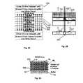
- FIG. 1Shows an overview of the prior art, and the single stage sensing architecture DRAMs.
- FIG. 2Shows details of the single stage sensing architecture.
- FIG. 3Schematically shows circuits for DRAM arrays, buffers, and shared global sense amplifiers.
- FIG. 4Shows sharing of buffers between two arrays through multiplexing.
- FIG. 5Shows circuit schematic of a cross-section of a differential signal datapath from the DRAM cell to data I/O.
- FIG. 6Shows an organization of multiple bit-lines and global bit-line datapaths in an embedded DRAM array.
- FIG. 1Shows an overview of the prior art, and the single stage sensing architecture DRAMs.
- FIG. 1Aa conventional DRAM macro with primary sense amplifiers and secondary sense amplifiers is shown.
- a plurality of memory cellsare arranged into arrays 100 .
- the first stage of sense amplifier-latches, located at each DRAM array, 150are used for sensing (reading) of the DRAM cell signals and the sensed data is stored in the latches.
- These primary amplifier-latches 150pass on signals through the global bit-lines, onto the corresponding second stage, shared global sense amplifiers 140 , for outputting to the corresponding dataline and I/O buffer external to the array.
- FIGS. 1B and 1Cshow arrangements of the single stage sensing architecture DRAMs.
- Buffers 110are located at each array 100 to amplify the bit-line signals for the global bit-lines, and also to isolate the bit-lines from the global bit-line loading and switching noises.
- the global sense amplifiers and latches 120are shared among all the DRAM arrays for sensing. Also, there are 120 the write circuits for writing to the DRAM cells through the global bit-lines and bit-lines during the Write-back phase of a Read/Write-back operation, or during a Refresh operation, or during a Write operation.
- FIG. 1Bshows a DRAM macro with the buffers 110 at each array, and the shared global sense amplifiers and latches 120 at the end of the macro.
- FIG. 1Cshows a DRAM macro with buffers 110 at each array, and two shared global sense amplifier banks 120 at each end of the macro.
- the two global sense amplifier bank structureis a variation to minimize the global bit-line wire delay, the top shared global sense amplifiers cover the sensing of the upper half of the arrays, and the bottom shared global sense amplifiers cover the sensing of the lower half of the arrays.
- FIG. 1 B and FIG. 1Cshows the buffers can be shared between two arrays through multiplexing (since only one array is active at a given time) to minimize area utilization. In an alternate embodiment, it is not necessary that a bank of buffers be shared among two arrays, in this case each array would have its own buffers without the use of multiplexing.
- FIG. 2Shows details of the single stage sensing architecture.
- FIG. 2Ais similar to FIG. 1C with the global bit-line 200 structure shown.
- FIG. 2Bis an expanded/detailed view of a portion of FIG. 2 A. It shows a buffer bank 110 with a cell array 100 on each side of it. In the array area there are individual memory cells 101 , bit-lines 210 and word-lines 220 .
- An individual buffers 111are shown driving global bit-lines 200 .
- a pair of global bit-lines 200inputs into a global sense amplifier 121 .
- the output of the global sense amplifier 121goes to data I/O 230 .
- FIG. 2Cshows the array area 100 in more detail. Again, word-line 220 , bit-line 210 , and cell 101 are shown. A voltage on a word-line 220 can activate a row of cells. Bit-lines from the array lead directly to the buffers 110 .
- FIG. 3Schematically shows circuits for DRAM arrays, buffers, and shared global sense amplifiers. This is a basic embodiment without multiplexing and a non-differential sense amplifier 121 .
- Cell 101is activated by word-line 220 and the charge from the cell reaches the buffer 111 through the bit-line 210 .
- the bufferdrives the global bit-line 200 , which inputs into the global sense amplifier and latch 121 .
- Write circuitry 320bypasses the global sense amplifier and buffer to reach the cell with the data from the outside during Write operations.
- Precharge circuits 310precharge the global 200 and local 210 bit-lines prior to Read operations.
- the bit-line 210 the global bit-line 200 and the sense amplifier 121together form the datapath, which connects a memory cell 101 to a data I/O 230 .
- FIG. 4Shows sharing of buffers between two arrays through multiplexing. Bit-lines 210 from two different arrays 420 and 421 bring signals of two different cells and a first multiplexing circuit 410 select which cell to become part of the datapath during a Read or Write operation.
- FIG. 5Shows circuit schematic of a cross-section of a differential signal datapath from the DRAM cell to data I/O.
- the global sense amplifier 500is a differential amplifier having two input ports in this embodiment. Two global bit-lines 501 and 502 are inputting to the global sense amplifier 500 .
- One of the global bit-liesis active the other one a dummy bit-line. Which one is the active and which one is the dummy depends on what cell was activated by the word-line.
- the global bit-line belonging to the datapath of the activated cellis the active bit-line.
- the gate of the buffer NFET 111is controlled by a voltage developed on the bit-line 210 from the DRAM cell 101 after the word-line 220 is activated. Only one word-line is activated throughout the macro.
- the NFETdrain to source discharges the voltage on the global bit-line 501 or 502 , which has been precharged to high (V dd ), slightly or heavily depending whether the DRAM cell stored a 0 or a 1.
- the gate voltage of the two different states(0 or 1), determines the drain-to-source current (Ids) through the NFET 111 and hence the rate of discharging the global bit-line voltage.
- the other differential (inactive) bit-line 501 or 502is held at V dd /2, assuming V dd /2 sensing, which the bit-lines are precharged to V dd /2.
- the differential signal on the two differential global bit-line 501 and 502is sensed by the shared, global differential sense amplifier 500 at the other end of the DRAM macro, producing a corresponding logic 1 or 0 at the output.
- each word-lineactivates N DRAM cells which are on alternating bit-lines. So when a word-line is activated, for each pair of bit-lines that are adjacent to each other, one bit-line is active with a DRAM cell being selected and the other one is inactive (DRAM cell not selected) with the bit-line voltage held at a precharged level.
- the inactive bit-linealso reduces noise coupling between adjacent bit-lines since its voltage is held roughly unchanged.
- the predetermined voltage on the inactive bit-lineserves as a reference point for differential sensing using two adjacent bit-lines, and in turn for the two adjacent global bit-lines and the two-input sense amplifier.
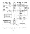
- FIG. 6Shows an organization of multiple bit-lines and global bit-line datapaths in an embedded DRAM array. It shows the detail structure, block diagram of a multiple array DRAM macro without primary sense amplifiers/latches, and a differential signal datapath to illustrate the read, write and refresh operation from DRAM cell to data I/O.
- the primary sense amplifiers/latchesare missing, and the differential bit-line pair is connected directly to the buffers which amplify the signals for the global bit-lines
- the column bit-switches 610are only for selecting the bit-lines among different arrays and can be combined with the array Read enable control and the array Write enable control
- dataare written back from the global sense amplifiers through write paths and write enable multiplexers to the bit-lines, as detailed in FIGS. 3, 4 , and 5 .
- each arraythere are the DRAM cells and the control gates, the word-lines, the (differential) bit-lines, bit-line precharge and bit-line multiplexing circuits.
- Each bit-line of each arrayis connected to the gate of a buffer driving the corresponding global bit-line, the buffer is controlled by an array Read enable signal during a Read operation.
- the differential signal from the differential bit-line pairis amplified by the buffers resulting a differential drain-source current discharging on the corresponding precharged pair of global bit-lines.
- a different voltageappears at the input of the corresponding shared global sense amplifier, for it to sense it as a 0 or 1.
- each write path of the global bit-lineis connected to the corresponding bit-line via a multiplexer enabled by an array Write enable signal. There is a precharge circuit for each global bit-line.
- the column bit-switchesare used for connecting the global bit-lines to the corresponding bit-lines of a particular array. In actual implementation, the column bit-switches are combined with the Read and Write enable circuits controlled by the array Read/Write control signals. Bit-line switches 610 are also the second multiplexing circuit, selecting between two possible bit-lines belonging to differing columns in a memory cell array.
- word-line access and bit-line sensingare done simultaneously by passing the developing bit-line signals to the global sense amplifier as soon as the word-line is activated without the explicit stage of setting primary sense amplifiers and closing of bit-line column switches, the control to read DRAM data can be simplified with less margin of error and overall read access time can be much reduced.
- the Read and Write-back operationscan be done in two cycles.
- First cycleis Read in which the data is read and stored in shared global sense amplifiers
- the second cycleis Write-back to the DRAM cell.
- the Refresh operationcan be done in two cycles.
- the bit-lines and global bit-lineshave to be precharged and the word-lines are turned ON and OFF.
- the Read datais stored at the end of the first cycle in the global sense amplifier, and is written back to the DRAM cell in the second cycle. In the two cycle operation, the cycle time is minimized.
- the Read and Write-back operationscan also be combined into a single cycle as practiced in conventional DRAM.
- the Read bit-switchesare turned OFF to separate global sense amplifiers from the global bit-lines.
- the Write bit-switchesare turned ON so the global sense amplifiers can write the data back to the DRAM cells via the global bit-lines.
- the speed of the DRAMis also helped by the fact that the word-line activation, sensing, and transferring the signals to the data output are operated in a self-timed fashion.
Landscapes
- Engineering & Computer Science (AREA)
- Microelectronics & Electronic Packaging (AREA)
- Computer Hardware Design (AREA)
- Dram (AREA)
Abstract
Description
Claims (18)
Priority Applications (3)
| Application Number | Priority Date | Filing Date | Title |
|---|---|---|---|
| US10/207,366US6768692B2 (en) | 2002-07-29 | 2002-07-29 | Multiple subarray DRAM having a single shared sense amplifier |
| TW092120246ATWI235374B (en) | 2002-07-29 | 2003-07-24 | Multiple subarray DRAM having a single shared sense amplifier |
| CNB031436382ACN1253896C (en) | 2002-07-29 | 2003-07-28 | Dynamic random access memory and method used for single level readout |
Applications Claiming Priority (1)
| Application Number | Priority Date | Filing Date | Title |
|---|---|---|---|
| US10/207,366US6768692B2 (en) | 2002-07-29 | 2002-07-29 | Multiple subarray DRAM having a single shared sense amplifier |
Publications (2)
| Publication Number | Publication Date |
|---|---|
| US20040017691A1 US20040017691A1 (en) | 2004-01-29 |
| US6768692B2true US6768692B2 (en) | 2004-07-27 |
Family
ID=30770415
Family Applications (1)
| Application Number | Title | Priority Date | Filing Date |
|---|---|---|---|
| US10/207,366Expired - LifetimeUS6768692B2 (en) | 2002-07-29 | 2002-07-29 | Multiple subarray DRAM having a single shared sense amplifier |
Country Status (3)
| Country | Link |
|---|---|
| US (1) | US6768692B2 (en) |
| CN (1) | CN1253896C (en) |
| TW (1) | TWI235374B (en) |
Cited By (11)
| Publication number | Priority date | Publication date | Assignee | Title |
|---|---|---|---|---|
| US20040240281A1 (en)* | 2003-05-30 | 2004-12-02 | Hynix Semiconductor Inc. | Sense amplifier select circuit and method of selecting the same |
| US20050052897A1 (en)* | 2003-09-05 | 2005-03-10 | Luk Wing K. | Single cycle read/write/writeback pipeline, full-wordline I/O DRAM architecture with enhanced write and single ended sensing |
| US20070153612A1 (en)* | 2005-12-29 | 2007-07-05 | Jae-Young Lee | Circuit and method of generating a boosted voltage in a semiconductor memory device |
| US20080170452A1 (en)* | 2007-01-11 | 2008-07-17 | Taek-Seon Park | Data output circuit in semiconductor memory device |
| US20100124135A1 (en)* | 2008-11-17 | 2010-05-20 | Samsung Electronics Co., Ltd. | Semiconductor memory devices having hierarchical bit-line structures |
| US20100172199A1 (en)* | 2008-11-11 | 2010-07-08 | Stmicroelectronics Pvt, Ltd. | Balanced sense amplifier for single ended bitline memory architecture |
| USRE42976E1 (en)* | 2002-10-29 | 2011-11-29 | Hynix Semiconductor, Inc. | Semiconductor memory device with reduced data access time |
| US8938589B2 (en) | 2010-01-28 | 2015-01-20 | Hewlett-Packard Development Company, L. P. | Interface methods and apparatus for memory devices using arbitration |
| US9146867B2 (en) | 2011-10-31 | 2015-09-29 | Hewlett-Packard Development Company, L.P. | Methods and apparatus to access memory using runtime characteristics |
| US9275686B2 (en) | 2014-05-28 | 2016-03-01 | Avago Technologies General Ip (Singapore) Pte. Ltd. | Memory banks with shared input/output circuitry |
| US9361955B2 (en) | 2010-01-28 | 2016-06-07 | Hewlett Packard Enterprise Development Lp | Memory access methods and apparatus |
Families Citing this family (9)
| Publication number | Priority date | Publication date | Assignee | Title |
|---|---|---|---|---|
| KR100670731B1 (en) | 2005-09-29 | 2007-01-17 | 주식회사 하이닉스반도체 | Semiconductor memory device |
| US20110227639A1 (en)* | 2010-03-19 | 2011-09-22 | Qualcomm Incorporated | Method and Apparatus for Suppressing Bitline Coupling Through Miller Capacitance to a Sense Amplifier Interstitial Node |
| US9419217B2 (en)* | 2011-08-15 | 2016-08-16 | Unity Semiconductor Corporation | Vertical cross-point memory arrays |
| US8958256B2 (en) | 2012-04-10 | 2015-02-17 | Micron Technology, Inc. | Apparatuses and methods for improved memory operation times |
| US10365851B2 (en) | 2015-03-12 | 2019-07-30 | Micron Technology, Inc. | Apparatuses and methods for data movement |
| US10048888B2 (en) | 2016-02-10 | 2018-08-14 | Micron Technology, Inc. | Apparatuses and methods for partitioned parallel data movement |
| ITUA20161478A1 (en) | 2016-03-09 | 2017-09-09 | St Microelectronics Srl | CIRCUIT AND METHOD OF READING A MEMORY CELL OF A NON-VOLATILE MEMORY DEVICE |
| US10074416B2 (en) | 2016-03-28 | 2018-09-11 | Micron Technology, Inc. | Apparatuses and methods for data movement |
| US20240242761A1 (en)* | 2021-05-05 | 2024-07-18 | Xenergic Ab | Burst access memory and method of operating a burst access memory |
Citations (15)
| Publication number | Priority date | Publication date | Assignee | Title |
|---|---|---|---|---|
| US5535172A (en)* | 1995-02-28 | 1996-07-09 | Alliance Semiconductor Corporation | Dual-port random access memory having reduced architecture |
| US5546349A (en)* | 1995-03-13 | 1996-08-13 | Kabushiki Kaisha Toshiba | Exchangeable hierarchical data line structure |
| US5610871A (en)* | 1993-11-30 | 1997-03-11 | Mitsubishi Denki Kabushiki Kaisha | Semiconductor memory device having a hierarchical bit line structure with reduced interference noise |
| US5625602A (en)* | 1991-11-18 | 1997-04-29 | Kabushiki Kaisha Toshiba | NAND-type dynamic RAM having temporary storage register and sense amplifier coupled to multi-open bit lines |
| US5774408A (en) | 1997-01-28 | 1998-06-30 | Micron Technology, Inc. | DRAM architecture with combined sense amplifier pitch |
| US5828594A (en)* | 1994-11-28 | 1998-10-27 | Fujitsu Limited | Semiconductor memory with hierarchical bit lines |
| US5886943A (en)* | 1996-09-18 | 1999-03-23 | Hitachi, Ltd. | Semiconductor memory having a hierarchical data line structure |
| US5889329A (en) | 1994-11-02 | 1999-03-30 | Lsi Logic Corporation | Tri-directional interconnect architecture for SRAM |
| US5923605A (en)* | 1997-09-29 | 1999-07-13 | Siemens Aktiengesellschaft | Space-efficient semiconductor memory having hierarchical column select line architecture |
| US6125071A (en)* | 1998-04-22 | 2000-09-26 | Kabushiki Kaisha Toshiba | Semiconductor memory device with high data read rate |
| US6378032B1 (en) | 2000-07-14 | 2002-04-23 | Texas Instruments Incorporated | Bank conflict avoidance in multi-bank DRAMS with shared sense amplifiers |
| US6480424B1 (en)* | 2001-07-12 | 2002-11-12 | Broadcom Corporation | Compact analog-multiplexed global sense amplifier for RAMS |
| US6545918B2 (en)* | 2000-06-13 | 2003-04-08 | Samsung Electronics Co., Ltd. | Semiconductor memory device having boosted voltage stabilization circuit |
| US6552944B2 (en) | 2001-05-31 | 2003-04-22 | International Business Machines Corporation | Single bitline direct sensing architecture for high speed memory device |
| US6633952B2 (en)* | 2000-10-03 | 2003-10-14 | Broadcom Corporation | Programmable refresh scheduler for embedded DRAMs |
Family Cites Families (2)
| Publication number | Priority date | Publication date | Assignee | Title |
|---|---|---|---|---|
| US5982203A (en)* | 1998-01-09 | 1999-11-09 | International Business Machines Corporation | Two stage SRCMOS sense amplifier |
| US6449202B1 (en)* | 2001-08-14 | 2002-09-10 | International Business Machines Corporation | DRAM direct sensing scheme |
- 2002
- 2002-07-29USUS10/207,366patent/US6768692B2/ennot_activeExpired - Lifetime
- 2003
- 2003-07-24TWTW092120246Apatent/TWI235374B/ennot_activeIP Right Cessation
- 2003-07-28CNCNB031436382Apatent/CN1253896C/ennot_activeExpired - Lifetime
Patent Citations (15)
| Publication number | Priority date | Publication date | Assignee | Title |
|---|---|---|---|---|
| US5625602A (en)* | 1991-11-18 | 1997-04-29 | Kabushiki Kaisha Toshiba | NAND-type dynamic RAM having temporary storage register and sense amplifier coupled to multi-open bit lines |
| US5610871A (en)* | 1993-11-30 | 1997-03-11 | Mitsubishi Denki Kabushiki Kaisha | Semiconductor memory device having a hierarchical bit line structure with reduced interference noise |
| US5889329A (en) | 1994-11-02 | 1999-03-30 | Lsi Logic Corporation | Tri-directional interconnect architecture for SRAM |
| US5828594A (en)* | 1994-11-28 | 1998-10-27 | Fujitsu Limited | Semiconductor memory with hierarchical bit lines |
| US5535172A (en)* | 1995-02-28 | 1996-07-09 | Alliance Semiconductor Corporation | Dual-port random access memory having reduced architecture |
| US5546349A (en)* | 1995-03-13 | 1996-08-13 | Kabushiki Kaisha Toshiba | Exchangeable hierarchical data line structure |
| US5886943A (en)* | 1996-09-18 | 1999-03-23 | Hitachi, Ltd. | Semiconductor memory having a hierarchical data line structure |
| US5774408A (en) | 1997-01-28 | 1998-06-30 | Micron Technology, Inc. | DRAM architecture with combined sense amplifier pitch |
| US5923605A (en)* | 1997-09-29 | 1999-07-13 | Siemens Aktiengesellschaft | Space-efficient semiconductor memory having hierarchical column select line architecture |
| US6125071A (en)* | 1998-04-22 | 2000-09-26 | Kabushiki Kaisha Toshiba | Semiconductor memory device with high data read rate |
| US6545918B2 (en)* | 2000-06-13 | 2003-04-08 | Samsung Electronics Co., Ltd. | Semiconductor memory device having boosted voltage stabilization circuit |
| US6378032B1 (en) | 2000-07-14 | 2002-04-23 | Texas Instruments Incorporated | Bank conflict avoidance in multi-bank DRAMS with shared sense amplifiers |
| US6633952B2 (en)* | 2000-10-03 | 2003-10-14 | Broadcom Corporation | Programmable refresh scheduler for embedded DRAMs |
| US6552944B2 (en) | 2001-05-31 | 2003-04-22 | International Business Machines Corporation | Single bitline direct sensing architecture for high speed memory device |
| US6480424B1 (en)* | 2001-07-12 | 2002-11-12 | Broadcom Corporation | Compact analog-multiplexed global sense amplifier for RAMS |
Non-Patent Citations (1)
| Title |
|---|
| "A 2.9ns Random Access Embedded DRAM with a Destructive-Read Architecture", C. Hwang et al, 2002 Symposium on VLSI Circuits, Digest of Technical Papers, Jun. 2002. |
Cited By (18)
| Publication number | Priority date | Publication date | Assignee | Title |
|---|---|---|---|---|
| USRE42976E1 (en)* | 2002-10-29 | 2011-11-29 | Hynix Semiconductor, Inc. | Semiconductor memory device with reduced data access time |
| US7057954B2 (en)* | 2003-05-30 | 2006-06-06 | Hynix Semiconductor Inc. | Sense amplifier select circuit and method of selecting the same |
| US20040240281A1 (en)* | 2003-05-30 | 2004-12-02 | Hynix Semiconductor Inc. | Sense amplifier select circuit and method of selecting the same |
| US20050052897A1 (en)* | 2003-09-05 | 2005-03-10 | Luk Wing K. | Single cycle read/write/writeback pipeline, full-wordline I/O DRAM architecture with enhanced write and single ended sensing |
| US7099216B2 (en)* | 2003-09-05 | 2006-08-29 | International Business Machines Corporation | Single cycle read/write/writeback pipeline, full-wordline I/O DRAM architecture with enhanced write and single ended sensing |
| US20070153612A1 (en)* | 2005-12-29 | 2007-07-05 | Jae-Young Lee | Circuit and method of generating a boosted voltage in a semiconductor memory device |
| US7548469B2 (en)* | 2005-12-29 | 2009-06-16 | Samsung Electronics Co., Ltd. | Circuit and method of generating a boosted voltage in a semiconductor memory device |
| US20080170452A1 (en)* | 2007-01-11 | 2008-07-17 | Taek-Seon Park | Data output circuit in semiconductor memory device |
| US7590010B2 (en)* | 2007-01-11 | 2009-09-15 | Samsung Electronics Co., Ltd. | Data output circuit in semiconductor memory device |
| US8144537B2 (en)* | 2008-11-11 | 2012-03-27 | Stmicroelectronics Pvt. Ltd. | Balanced sense amplifier for single ended bitline memory architecture |
| US20100172199A1 (en)* | 2008-11-11 | 2010-07-08 | Stmicroelectronics Pvt, Ltd. | Balanced sense amplifier for single ended bitline memory architecture |
| US8120979B2 (en)* | 2008-11-17 | 2012-02-21 | Samsung Electronics Co., Ltd. | Semiconductor memory devices having hierarchical bit-line structures |
| US20100124135A1 (en)* | 2008-11-17 | 2010-05-20 | Samsung Electronics Co., Ltd. | Semiconductor memory devices having hierarchical bit-line structures |
| KR101461632B1 (en) | 2008-11-17 | 2014-11-13 | 삼성전자주식회사 | A semiconductor memory device having a hierarchical bit line structure |
| US8938589B2 (en) | 2010-01-28 | 2015-01-20 | Hewlett-Packard Development Company, L. P. | Interface methods and apparatus for memory devices using arbitration |
| US9361955B2 (en) | 2010-01-28 | 2016-06-07 | Hewlett Packard Enterprise Development Lp | Memory access methods and apparatus |
| US9146867B2 (en) | 2011-10-31 | 2015-09-29 | Hewlett-Packard Development Company, L.P. | Methods and apparatus to access memory using runtime characteristics |
| US9275686B2 (en) | 2014-05-28 | 2016-03-01 | Avago Technologies General Ip (Singapore) Pte. Ltd. | Memory banks with shared input/output circuitry |
Also Published As
| Publication number | Publication date |
|---|---|
| TWI235374B (en) | 2005-07-01 |
| US20040017691A1 (en) | 2004-01-29 |
| CN1476020A (en) | 2004-02-18 |
| CN1253896C (en) | 2006-04-26 |
| TW200410252A (en) | 2004-06-16 |
Similar Documents
| Publication | Publication Date | Title |
|---|---|---|
| US6768692B2 (en) | Multiple subarray DRAM having a single shared sense amplifier | |
| KR100211760B1 (en) | Data I / O Path Control Circuit of Semiconductor Memory Device with Multi-Bank Structure | |
| US9135986B2 (en) | Systems and methods of sectioned bit line memory arrays, including hierarchical and/or other features | |
| JP4331966B2 (en) | Semiconductor integrated circuit | |
| US7417911B2 (en) | Semiconductor memory device having hierarchically structured data lines and precharging means | |
| US7099216B2 (en) | Single cycle read/write/writeback pipeline, full-wordline I/O DRAM architecture with enhanced write and single ended sensing | |
| US6359813B1 (en) | Semiconductor memory device having improved data transfer rate without providing a register for holding write data | |
| US7471590B2 (en) | Write control circuitry and method for a memory array configured with multiple memory subarrays | |
| US8520449B2 (en) | Semiconductor device and control method thereof | |
| US6678198B2 (en) | Pseudo differential sensing method and apparatus for DRAM cell | |
| US6249471B1 (en) | Fast full signal differential output path circuit for high-speed memory | |
| US7468925B2 (en) | Semiconductor memory device realizing high-speed access | |
| EP0573046B1 (en) | Semiconductor memory device with single data line pair shared between memory cell arrays | |
| US7289385B2 (en) | Bank selection signal control circuit for use in semiconductor memory device, and bank selection control method | |
| CN101206917A (en) | Semiconductor integrated circuit and method of operating the same | |
| US5828613A (en) | Random-access memory | |
| KR100442225B1 (en) | Semiconductor memory device capable of reading at high speed | |
| US7095673B2 (en) | Semiconductor memory device capable of operating at high speed | |
| US6434069B1 (en) | Two-phase charge-sharing data latch for memory circuit | |
| US20230238051A1 (en) | Systems, apparatuses and methods for precharging digit lines | |
| KR0133273B1 (en) | Semiconductor memory device | |
| JP3766710B2 (en) | Semiconductor memory device | |
| JP2009176419A (en) | Data processor | |
| JP2006092696A (en) | Buffer circuit and semiconductor storage device using the same |
Legal Events
| Date | Code | Title | Description |
|---|---|---|---|
| AS | Assignment | Owner name:INTERNATIONAL BUSINESS MACHINES CORPORATION, NEW Y Free format text:ASSIGNMENT OF ASSIGNORS INTEREST;ASSIGNORS:LUK, WING K.;KIRIHATA, TOSHIAKI K.;REEL/FRAME:013188/0185;SIGNING DATES FROM 20020725 TO 20020729 | |
| FEPP | Fee payment procedure | Free format text:PAYOR NUMBER ASSIGNED (ORIGINAL EVENT CODE: ASPN); ENTITY STATUS OF PATENT OWNER: LARGE ENTITY | |
| STCF | Information on status: patent grant | Free format text:PATENTED CASE | |
| FPAY | Fee payment | Year of fee payment:4 | |
| REMI | Maintenance fee reminder mailed | ||
| FPAY | Fee payment | Year of fee payment:8 | |
| SULP | Surcharge for late payment | Year of fee payment:7 | |
| AS | Assignment | Owner name:GLOBALFOUNDRIES U.S. 2 LLC, NEW YORK Free format text:ASSIGNMENT OF ASSIGNORS INTEREST;ASSIGNOR:INTERNATIONAL BUSINESS MACHINES CORPORATION;REEL/FRAME:036550/0001 Effective date:20150629 | |
| AS | Assignment | Owner name:GLOBALFOUNDRIES INC., CAYMAN ISLANDS Free format text:ASSIGNMENT OF ASSIGNORS INTEREST;ASSIGNORS:GLOBALFOUNDRIES U.S. 2 LLC;GLOBALFOUNDRIES U.S. INC.;REEL/FRAME:036779/0001 Effective date:20150910 | |
| FPAY | Fee payment | Year of fee payment:12 | |
| AS | Assignment | Owner name:WILMINGTON TRUST, NATIONAL ASSOCIATION, DELAWARE Free format text:SECURITY AGREEMENT;ASSIGNOR:GLOBALFOUNDRIES INC.;REEL/FRAME:049490/0001 Effective date:20181127 | |
| AS | Assignment | Owner name:GLOBALFOUNDRIES U.S. INC., CALIFORNIA Free format text:ASSIGNMENT OF ASSIGNORS INTEREST;ASSIGNOR:GLOBALFOUNDRIES INC.;REEL/FRAME:054633/0001 Effective date:20201022 | |
| AS | Assignment | Owner name:GLOBALFOUNDRIES INC., CAYMAN ISLANDS Free format text:RELEASE BY SECURED PARTY;ASSIGNOR:WILMINGTON TRUST, NATIONAL ASSOCIATION;REEL/FRAME:054636/0001 Effective date:20201117 | |
| AS | Assignment | Owner name:GLOBALFOUNDRIES U.S. INC., NEW YORK Free format text:RELEASE BY SECURED PARTY;ASSIGNOR:WILMINGTON TRUST, NATIONAL ASSOCIATION;REEL/FRAME:056987/0001 Effective date:20201117 |