US6768685B1 - Integrated circuit memory array with fast test mode utilizing multiple word line selection and method therefor - Google Patents
Integrated circuit memory array with fast test mode utilizing multiple word line selection and method thereforDownload PDFInfo
- Publication number
- US6768685B1 US6768685B1US09/990,894US99089401AUS6768685B1US 6768685 B1US6768685 B1US 6768685B1US 99089401 AUS99089401 AUS 99089401AUS 6768685 B1US6768685 B1US 6768685B1
- Authority
- US
- United States
- Prior art keywords
- line
- read
- lines
- memory cells
- invention defined
- Prior art date
- Legal status (The legal status is an assumption and is not a legal conclusion. Google has not performed a legal analysis and makes no representation as to the accuracy of the status listed.)
- Expired - Lifetime
Links
Images


Classifications
- G—PHYSICS
- G11—INFORMATION STORAGE
- G11C—STATIC STORES
- G11C29/00—Checking stores for correct operation ; Subsequent repair; Testing stores during standby or offline operation
- G11C29/04—Detection or location of defective memory elements, e.g. cell constructio details, timing of test signals
- G11C29/08—Functional testing, e.g. testing during refresh, power-on self testing [POST] or distributed testing
- G11C29/12—Built-in arrangements for testing, e.g. built-in self testing [BIST] or interconnection details
- G11C29/18—Address generation devices; Devices for accessing memories, e.g. details of addressing circuits
- G11C29/30—Accessing single arrays
- G11C29/34—Accessing multiple bits simultaneously
- G—PHYSICS
- G11—INFORMATION STORAGE
- G11C—STATIC STORES
- G11C29/00—Checking stores for correct operation ; Subsequent repair; Testing stores during standby or offline operation
- G11C29/04—Detection or location of defective memory elements, e.g. cell constructio details, timing of test signals
- G11C29/08—Functional testing, e.g. testing during refresh, power-on self testing [POST] or distributed testing
- G11C29/12—Built-in arrangements for testing, e.g. built-in self testing [BIST] or interconnection details
- G11C2029/1202—Word line control
- G—PHYSICS
- G11—INFORMATION STORAGE
- G11C—STATIC STORES
- G11C29/00—Checking stores for correct operation ; Subsequent repair; Testing stores during standby or offline operation
- G11C29/04—Detection or location of defective memory elements, e.g. cell constructio details, timing of test signals
- G11C29/08—Functional testing, e.g. testing during refresh, power-on self testing [POST] or distributed testing
- G11C29/12—Built-in arrangements for testing, e.g. built-in self testing [BIST] or interconnection details
- G11C29/18—Address generation devices; Devices for accessing memories, e.g. details of addressing circuits
- G11C29/26—Accessing multiple arrays
- G11C2029/2602—Concurrent test
Definitions
- the present inventionrelates to semiconductor integrated circuit memory arrays, and particularly those incorporating write-once passive element memory cells incorporating anti-fuses.
- write-once memory arraysalso known as one-time programmable, or OTP memory arrays
- OTP memory arraysparticularly those incorporating anti-fuse memory cells
- One such problemconcerns testing each unprogrammed memory cell, for it is desirable to test each memory cell to ensure that the unprogrammed state (e.g., high-impedance state) exists at every memory cell location.
- a standard read mode testcan be employed to ensure this.
- the test time required to perform such a read mode test of every memory cellis significant, especially in a very large array such as a three dimensional memory array having upwards of a billion memory cells. Such long test times contribute to increased product manufacturing cost.
- Multiple memory cells on a single bit linemay be tested in parallel for the unprogrammed state by simultaneously selecting multiple word lines associated with a selected bit line within a sub-array. A read current flowing through each selected memory cell is added on the selected bit line, thus logically performing an OR function of any selected memory cell found to be in the programmed state. The total read current through one or more selected memory cells onto the selected bit line may be sensed using the same bit line sense circuits used for normal read operations. Separate sense amplifiers may also be used, but are not required, nor is any complicated BIST (i.e., built-in-self-test) logic.
- the word line decoding circuitrypreferably responds to a test mode signal to cause more than one word line to be selected in the test mode.
- the test mode signalcauses a portion of the row address signals to be ignored, which allows more than one word line to be selected.
- the ignored address signalsrepresent low-order row address signals and consequently the multiply selected word lines are all adjacent to each other in a contiguous block within a sub-array.
- Exemplary numbers of simultaneously selected world linesinclude 4, 8, 16, 32, or 64 word lines, with 16 such simultaneously selected word lines being particularly preferred.
- a sense circuitis preferably coupled to the selected bit line and generates a read signal which, in the test mode, indicates a pass/fail condition for all N simultaneously selected memory cells.
- a pass/fail indicationmay be directly conveyed as an output signal of the integrated circuit, or may be combined with other similar pass/fail signals from other selected bit line sense circuits to generate a combined pass/fail signal representing an even greater number of simultaneously tested memory cells which is then conveyed as an output signal.
- Multiple bit linesmay be simultaneously selected within the same sub-array to each generate a multiple respective pass/fail signals which are then combined into fewer numbers of output signals.
- multiple sub-arraysmay be simultaneously selected, each having one or more simultaneously selected bit lines, and the respective pass/fail signals conveyed directly or combined into fewer numbers of such signals, including just one such combined pass/fail signal.
- the pass/fail signalsmay be generated to also indicate a third (e.g., ‘marginal’) condition, upon which additional and/or more thorough testing may be initiated for the affected memory cells.
- the inventionmay be advantageously applied to parallel testing of memory cells which have a low-current and a high-current state and which contribute such current, when selected, onto an associated bit line. It is particularly useful for testing passive element memory cells to ensure that each memory cell remains in its low current state. Passive element memory cells having anti-fuse elements may be tested in parallel to ensure that each remains in its unprogrammed (i.e., high impedance) state or that no other manufacturing defects are present which contribute current flow onto a selected bit line.
- the inventionis particularly well-suited to three-dimensional memory arrays (i.e., having more than one plane of memory cells) incorporating anti-fuse passive element memory cells.
- word lines from each of two layers that are both associated with a single bit line layermay be simultaneously selected to test in parallel memory cells located in two adjacent memory planes.
- FIG. 1is a block diagram of a memory array and supporting row and column circuits.
- FIG. 2is an electrical schematic diagram representing a passive element memory array, showing a selected word line (indicated as an X-line), a group of unselected word lines, a selected bit line (indicated as a Y-line), and a group of unselected bit lines, typical of a normal read mode.
- FIG. 3is an electrical schematic diagram representing a passive element memory array, showing a group of selected X-lines, a group of unselected X-lines, and a selected Y-line, depicted during a test mode in accordance with the present invention.
- FIG. 4is a waveform diagram of signals within the circuit depicted in FIG. 3 .
- FIG. 5is an electrical schematic diagram of an embodiment of row select circuits useful for the present invention.
- FIG. 6is a block diagram showing a group of selected X-lines, and two selected Y-lines, depicted during a test mode in accordance with an embodiment of the present invention.
- FIG. 7is a block diagram showing a plurality of sub-arrays, each generating a read signal during a test mode which are combined into a single output signal.
- FIG. 8is a block diagram showing a plurality of sub-arrays, each generating a read signal during a test mode which are respectively conveyed as independent output signals.
- FIG. 9is a block diagram of a useful arrangement of sub-arrays for use with certain embodiments of the present invention.
- FIG. 10is a block diagram depicting a preferred arrangement of various row select circuits for a particular sub-array.
- the memory array 102is preferably a three-dimensional, non-volatile, field-programmable write-once memory array of passive element memory cells, although other memory arrays are also suitable and specifically contemplated.
- Each passive element memory cell within the memory array 102is generally a two-terminal memory cell having a steering element in series with a state change element, together connected between usually orthogonal (but not necessarily so) array terminal lines. These two elements within a memory cell may both be present before programming. Alternatively, the steering element within a given memory cell may be formed during programming of the memory cell.
- Suitable state change elementsinclude those having a significant change of resistance, including both fuses and antifuses.
- a memory cell whose state change element is an antifusemay be termed an antifuse memory cell, whereas a memory cell whose state change element is a fuse may be termed a fuse memory cell.
- An advantageous passive element memory cellis a structure combining an antifuse and a diode in series as the memory cell.
- Particularly suitable memory cellsare described in U.S. patent application Ser. No. 09/897,705 entitled “Three-Dimensional Memory Array Incorporating Serial Chain Diode Stack” filed on Jun. 29, 2001, U.S. patent application Ser. No. 09/814,727 entitled “Three-Dimensional Memory Array and Method of Fabrication” filed on Mar. 21, 2001, U.S. patent application Ser. No. 09/560,626 entitled “Three-Dimensional Memory Array and Method of Fabrication” filed on Apr. 28, 2000, and in U.S. Pat. No. 6,034,882 entitled “Vertically Stacked Field Programmable Nonvolatile Memory and Method of Fabrication,”, each of which are hereby incorporated by reference in their entirety.
- the array terminal lines at one levelmay be termed word lines or X-lines.
- the array terminal lines at a vertically adjacent levelmay be termed bit lines or Y-lines.
- a memory cellis formed at the intersection of each word line and each bit line, and is connected between the respective intersecting word line and bit line.
- a three-dimensional memory array which has at least two levels of memory cellsmay utilize at least more than one layer of word lines or more than one layer of bit lines.
- a group of word lines, each residing on a separate layer (i.e., level) and substantially vertically-aligned (notwithstanding small lateral offsets on some layers),may be collectively termed a row.
- the word lines within a rowpreferably share at least a portion of the row address.
- bit lineseach residing on a separate layer and substantially vertically-aligned (again, notwithstanding small lateral offsets on some layers), may be collectively termed a column.
- the bit lines within a columnpreferably share at least a portion of the column address.
- the array terminals of memory array 102include the various layer(s) of word lines organized as rows, and the various layer(s) of bit lines organized as columns.
- the integrated circuit 100includes a row circuits block 104 whose outputs 108 are connected to respective word lines of the memory array 102 .
- the row circuits block 104receives a group of M row address signals and one or more various control signals, and typically may include such circuits as row decoders and array terminal drivers for both read and write (i.e., programming) operations.
- the integrated circuit 100also includes a column circuits block 106 whose input/outputs 110 are connected to respective bit lines of the memory array 102 .
- the column circuits block 106receives a group of N column address signals and one or more various control signals, and typically may include such circuits as column decoders, array terminal receivers, read/write circuitry, and I/O multiplexers. Circuits such as the row circuits block 104 and the column circuits block 106 may be collectively termed array terminal circuits for their connection to the various terminals of the memory array 102 .
- Integrated circuits incorporating a memory arrayusually subdivide the array into a sometimes large number of sub-arrays.
- a sub-arrayis a contiguous group of memory cells having contiguous word and bit lines generally unbroken by decoders, drivers, sense amplifiers, and input/output circuits. This is done for any of a variety of reasons. For example, the signal delays traversing down word lines and bit lines which arise from the resistance and the capacitance of such lines (i.e., the RC delays) may be very significant in a large array. These RC delays may be reduced by subdividing a larger array into a group of smaller sub-arrays so that the length of each word line and/or each bit line is reduced.
- the power associated with accessing a group of memory cellsmay dictate an upper limit to the number of memory cells which may be accessed simultaneously during a given memory cycle. Consequently, a large memory array is frequently subdivided into smaller sub-arrays to decrease the number of memory cells which are simultaneously accessed. Nonetheless, for ease of description, an array may also be used synonymously with sub-array to refer to a contiguous group of memory cells having contiguous word and bit lines generally unbroken by decoders, drivers, sense amplifiers, and input/output circuits. As used herein, an integrated circuit may include one or more than one memory array.
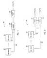
- FIG. 2depicts a representation of a single layer of X-lines (e.g., word lines) and a single layer of Y-lines (e.g., bit lines) within a single sub-array 120 .
- X-linese.g., word lines
- Y-linese.g., bit lines
- FIG. 2depicts a representation of a single layer of X-lines (e.g., word lines) and a single layer of Y-lines (e.g., bit lines) within a single sub-array 120 .
- a selected X-line 122 and a group of five unselected X-lines 124are shown
- a selected Y-line 126 and group of three unselected Y-lines 128are shown. It is understood that many more such X-lines and Y-lines are usually encountered in a memory array, but the few shown are sufficient to introduce the relevant concepts.
- the memory array 120includes antifuse memory cells, although other types of passive element memory cells are contemplated, as well as certain other types of memory cells, described later.
- a selected memory cell 130is shown coupled between the selected X-line 122 and the selected Y-line 126 . A small number of other memory cells are depicted, although it should be understood that a memory cell normally is formed at each intersection of an X-line and a Y-line (not shown).
- Each of the X-lines shownare coupled to an X-Line Select Circuits block 132 (which is typically part of the row circuits block 104 ), and each of the Y-lines shown are coupled to a Y-Line Select and Sense Circuit block 134 (which is typically part of the column circuits block 106 ).
- the X-Line Select Circuits block 132normally selects one particular X-Line in the sub-array by decoding a group of address signals (not shown) and driving the particular X-line to a read bias voltage suitable for a selected X-line.
- the Y-Line Select and Sense Circuit block 134normally selects one particular Y-Line by decoding another group of address signals (not shown) and coupling a sense circuit to the selected Y-line.
- the selected Y-lineis also biased at a read bias voltage suitable for a selected Y-line, frequently by the sense circuit itself, or alternatively, by a separate bias circuit.
- the memory arrayis a fully-decoded array which selects no more than one X-line and one Y-line within a given sub-array to access an associated bit of data.
- a filly decoded arrayincludes those that access more than one bit of data simultaneously, and also those having at least one dimension not equal to an integral power of two.
- Logic array structures implementing only a portion of the minterms of its input variablesare not considered to be fully-decoded arrays.
- the respective read bias voltages for the selected X-line and the selected Y-lineare preferably chosen to place a forward bias voltage across the selected memory cell so that current flow through the selected memory cell, if any, may be detected.
- the selected X-line 122is preferably driven to a read bias voltage of about 2.0 volts
- the selected Y-line 126is driven (i.e., biased at) about ground.
- the unselected X-lines and unselected Y-linesare biased to respective voltages to reduce or eliminate any significant forward bias voltage across unselected memory cells, with the unselected X-lines preferably biased at or near ground, and the unselected Y-lines preferably biased at or near 2.0 volts.
- bias voltagesmay be advantageously chosen which are compatible with the particular memory cell technology employed.
- Particularly suitable bias conditions for a three-dimensional array of non-volatile anti-fuse passive element memory cellsare described in U.S. application Ser. No. 09/897,771, entitled “Method and Apparatus for Biasing Selected and Unselected Array Lines When Writing a Memory Array”, by Roy E. Scheuerlein, which application is hereby incorporated by reference in its entirety.
- the selected memory cell 130remains unprogrammed in its high impedance (i.e., low current) state, then a negligible amount of current will flow from the selected X-line 122 into the selected Y-line 126 . But if the selected memory cell 130 has been programmed to a low impedance (i.e., high current) state, then that “high” amount of current will flow from the selected X-line 122 into the selected Y-line 126 , which current may be detected by the Y-Line Select and Sense Circuit block 134 and buffered to generate a read data signal 136 . It should be appreciated that in other embodiments having memory cells forward biased from a Y-line to an X-line, cell current may instead flow from a Y-line to an X-line.
- each Y-linemay be simultaneously selected that are each associated with a single selected X-line, and each Y-line is typically biased and sensed with a corresponding sense circuit to generate a multi-bit read data output (not shown).
- each of the memory cells associated with a given Y-linemay be individually determined to be in its respective low-current or high-current state, multiple X-lines are not simultaneously selected, but rather a single X-line is selected from those X-lines associated with a given Y-line.
- each X-lineis traditionally individually selected to determine if the corresponding memory cell presents a high impedance to the Y-line sense circuit. With memory densities approaching billions of memory cells on a single integrated circuit, such testing may consume considerable time and lead to increased manufacturing costs.
- FIG. 3a portion of the memory array 120 is shown.
- the selected Y-line 126 and internal portions of an exemplary Y-Line Select and Sense Circuit block 134are depicted.
- the X-Line Select Circuits block 132is shown, which receives a TEST signal conveyed on node 150 .
- the X-Line Select Circuits block 132simultaneously selects more than one X-line rather than just selecting one X-line as before.
- a group of selected X-lines 142is shown, including the X-line 122 that would have been selected before (assuming the same ‘row’ or X-line address), as well as two additional selected X-lines 146 and 148 .
- Each of the simultaneously selected X-linesis associated with the selected Y-line 126 .
- Each respective memory cell that is coupled between a respective selected X-line and the selected Y-lineis selected and potentially contributes current into the selected Y-line 126 , which may be detected, as before, using normal read circuits within the Y-Line Select and Sense Circuit block 134 .
- the current flowing into the selected Y-line 126is the sum of any current flowing from selected X-line 122 through selected memory cell 130 , any current flowing from selected X-line 146 through selected memory cell 147 , and any current flowing from selected X-line 148 through selected memory cell 149 . If a “low total current” flows into the selected Y-line 126 , then all selected memory cells are known to remain in a low-current state, and need not be individually addressed and sensed to determine such a condition. However, if the current into the selected Y-line 126 is a “high” current, then one or more selected memory cells is in a high current state, or a defect exists which allows such an excessive current to flow.
- An exemplary Y-Line Select and Sense Circuit block 134is depicted which includes a Y-line select block 152 coupling the selected Y-line 126 to a sense circuit 155 .
- Suitable select blocksare well known in the art.
- Such a select block 152may take a variety of suitable forms, and may be implemented as a portion of a bit line driver circuit configured to also drive its associated bit line, when unselected, to an unselected read bias voltage, and to other voltages during other times.
- An exemplary select block 152receives a BLSELECT signal, such as from a column decoder (not shown).
- the select block 152couples its associated Y-line to a common node, such as sense node 154 , serving a group of Y-lines, and when the BLSELECT is inactive, the select block 152 drives the Y-line to an unselected Y-line bias voltage V UYL (here shown as approximately +2.0 volts).
- a precharge transistor 156is momentarily activated by a precharge signal PRE to drive node 154 to ground, which also grounds the selected Y-line 126 through the Y-line select block 152 .
- An amplifier 158is configured to compare the voltage of node 154 to a reference voltage V REF and generate accordingly a read data signal READ on an output node 162 .
- the value of the reference voltage V REFis preferably chosen to be near the mid-point between the voltage of a selected Y-line when pulled high through a selected memory cell (i.e., the bias voltage of a selected X-line less the voltage drop across a selected memory cell) and ground.
- V REF voltageis approximately 250 mV (for a selected X-line voltage V SXL of approximately 2.0 volts). If a significant current flows into the selected Y-line 126 , the voltage of the selected Y-line 126 and the voltage of node 154 will increase to a voltage greater than the reference voltage V REF at which time the READ signal is driven high. If, alternatively, a negligible current flows into the selected Y-line 126 , the voltage of the selected Y-line 126 and the voltage of node 154 will remain at or near ground (and particularly will remain below the reference voltage V REF ) and the READ signal will remain low.
- V SENSEThe voltage of the sense node 154 (i.e., V SENSE ) is plotted for each of several situations. Initially, the V SENSE voltage is discharged from an initial unselected Y-line voltage V UYL to ground by the precharge transistor 156 , which is shown by curve 180 . If one or more selected memory cells have been programmed, the read current causes the V SENSE voltage to increase well above the V REF voltage, as shown by curve 182 .
- the read current through N selected memory cells and into the selected Y-line 126causes the V SENSE voltage to increase only slightly, thus remaining near ground, and in particular, below the V REF voltage, as shown by curve 184 .
- the read current through one selected memory cellcauses the V SENSE voltage to increase even less, thus remaining even closer to ground, as shown by curve 186 .
- the same sense circuit normally used for reading a selected memory cell in the normal read modemay be used without modification when in the test mode to sense the plurality of simultaneously selected memory cells.
- Many suitable Y-line select block circuits and read or sense circuitsmay be employed as well, including various clamped bit line sense circuits, and including schemes incorporating noise detection lines, such as those described in U.S. application Ser. No. 09/896,468, entitled “Current Sensing Method and Apparatus Particularly Useful for a Memory Array of Cells Having Diode-Like Characteristics” by Scheuerlein, and in U.S. application Ser. No.
- V REFvoltage conveyed on node 160
- a reference voltagesuch as the V REF voltage conveyed on node 160
- the higher combined leakage current of N selected memory cellscauses a higher voltage on the sense node 154 (shown as curve 184 ) than for a single selected memory cell (shown as curve 186 ).
- the magnitude of V REFmay be adjusted upward to provide better margins for the higher anticipated bit line current during the test mode. It is also contemplated to use one or more sense circuits for the test mode which are separate from those used in the normal read mode.
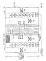
- a X-line select circuit 200which includes a plurality of pre-decoders 201 driving a plurality of decoder/drivers 226 .
- the predecoders 201are arranged to pre-decode three groups of addresses.
- Eight pre-decode circuits 204are arranged to receive the eight combinations of three addresses A 9 , A 8 , and A 7 and consequently generate a group of eight pre-decoded lines XL, a selected one of which is driven active low, and which collectively are conveyed on the XL pre-decode bus 220 .
- eight pre-decode circuits 206are arranged to receive the eight combinations of addresses A 6 , A 5 , and A 4 and consequently generate a group of eight pre-decoded lines XM, a selected one of which is driven active low, and which collectively are conveyed on the XM pre-decode bus 222 .
- sixteen pre-decode circuits 208are arranged to receive the eight combinations of four addresses A 3 , A 2 , A 1 , and A 0 and consequently generate a group of sixteen pre-decoded lines XP, a selected one of which is driven active low during the normal read mode of operation, and which collectively are conveyed on the XP pre-decode bus 224 .
- a first such row decoder for an X-line Ais arranged to receive one of the eight XL lines, one of the eight XM lines, and one of the sixteen XP lines, each conveyed to decoder NOR gate 228 to generate a 1 of 1024 active high decoded signal on its output node 227 .
- This signalis preferably buffered by a level translator 230 and driver 232 and conveyed to the X-line A.
- Both the level translator 230 and the driver 232are configured to generate suitable bias voltages for at times reading and at other times writing passive element memory cells. As shown in the figure, the voltages are appropriate for the read mode and test mode of interest here. Specifically, a voltage conveyed on bus 229 to the level translator circuit 230 provides the output high level for the translator circuit, which in the read mode is preferably about 2.0 volts (for this exemplary embodiment).
- the driver circuit 232is arranged to receive the output 231 from the translator circuit 230 , and accordingly drive its output (i.e., X-line A) to a high level equal to the voltage conveyed on bus 233 (also the V READ voltage of about 2.0 volts) or to a low level equal to the voltage conveyed on bus 235 .
- a second such row decoder for an X-line Bis arranged to receive a different one of the eight XL lines, a different one of the eight XM lines, and a different one one of the sixteen XP lines, each conveyed to decoder NOR gate 234 to generate another 1 of 1024 active high decoded signal on its output node, which is buffered by level translator 236 and driver 238 to drive the X-line B.
- Other decoder and driver circuitsmay be employed, depending on the memory technology and the array configuration chosen. Useful word line circuits and configurations are described in “Three-Dimensional Memory Array Incorporating Serial Chain Diode Stack,” application Ser. No. 09/897,705, filed on Jun.
- the pre-decode NAND gate 212 outputis followed by a two-input NAND gate 214 rather than followed by just a buffer (as in the other two pre-decoders 204 and 206 ).
- an XAFTEST signalis asserted and conveyed on node 210 to the other input of this NAND gate 214 to inhibit or override the addresses otherwise pre-decoded.
- XAFTESTis asserted, all sixteen pre-decode lines XP are driven low, and since these lines are active low, sixteen of the decoders 226 are selected rather than just one, and consequently sixteen X-lines are driven to the read voltage V READ .
- a gating signal XRGATEis provided which is asserted only after all address signals to the various pre-decoders have stabilized.
- this XRGATE signalBy conveying this XRGATE signal to a fourth input of NAND gate 202 , the selected one-of-eight XL predecode signals is asserted only after all other pre-decode signals have been properly decoded, and spurious row decodes in the row decoders 226 are avoided.
- X-linesmay achieve a greater or lesser number of simultaneously selected X-lines during the test mode.
- suitable techniques and circuitsmay be employed to simultaneously drive more than one X-line to a suitable read bias voltage.
- a totally different driver circuitmay be employed and the normal row decoder circuitry disabled.
- a row decoder circuitmay be arranged with a shift-register style test mode decoder which sequentially shifts a test mode signal through a plurality of stages to select more than one (or all) such decoder outputs.
- the READ signal conveyed on node 162may be interrogated to assess sixteen memory cells at a time.
- Such a READ signalmay be conveyed directly as an output signal, or another signal derived from the READ signal may instead be conveyed as an output to communicate the result. All the memory cells in the array may be tested by cycling through the non-inhibited addresses. In other embodiments 4, 8, 32, or 64 X-lines may be simultaneously selected.
- This conceptmay be extended by simultaneously selecting more than one Y-line associated with a group of selected X-lines in a sub-array.
- a sub-array 250is depicted having two selected Y-lines 126 and 256 during the test mode.
- the X-line select circuits block 132receives a TEST signal to cause a plurality of X-lines 252 to be simultaneously selected, while a plurality of X-lines 262 remains unselected.
- the first selected Y-line 126 and a plurality of unselected Y-lines 258are conveyed to a Y-select and sense circuit 132 which generates a READ signal on node 162 , as before.
- a second selected Y-line 256 and a second plurality of unselected Y-lines 260are conveyed to a second Y-select and sense circuit 264 which generates a corresponding READ signal on node 268 .
- These two read signalsare combined in a combiner circuit 266 and buffered by an output circuit 270 to generate a single pass/fail signal as an output signal of the integrated circuit.
- Suitable combiner circuitsinclude simple logic circuits which are well known in the art.
- both READ signalsmay be independently conveyed as two output signals. Additional selected Y-lines may be provided in a single sub-array, whose outputs may be combined into a smaller number of output signals, including down to just one such output signal for the entire sub-array.
- a memory arrayis implemented as multiple sub-arrays, the concept may be further extended by operating each sub-array as described above, and combining one or more READ signals from each sub-array, or one or more signals derived from the READ signals from each array, into one or more output signals for the entire memory array.
- FIG. 7a block diagram is shown of a memory array 280 having a plurality of sub-arrays, each generating in the test mode a respective signal for indicating the test status of a selected group of memory cells associated with one or more selected Y-lines within the respective sub-array.
- Two sub-arrays 282 and 284are depicted, although it should be understood that in practice many more such sub-arrays are usually implemented.
- Sub-arrays 282 and 284generate respective read signals 286 and 288 , which are combined in a block 290 and buffered by output circuit 292 to generate a single PASS/FAIL output signal.
- a memory array 300is shown having a plurality of sub-arrays, each generating in the test mode a respective signal for indicating the test status of a selected group of memory cells associated with one or more selected Y-lines within the respective sub-array.
- sub-arrays 302 and 304generate respective read signals 306 and 308 , which are independently buffered by respective output circuits 310 and 312 to generate respective PASS/FAIL output signals.
- a significant decrease in test timemay be accomplished if such a test mode is carried out in a large number of such sub-arrays.
- the memory arrayis divided into 72 sub-arrays as shown in FIG. 9 .
- Eight error correction check/syndrome bitsare concatenated to each 64 bit data word to generate a 72-bit ECC data word.
- each bit of this 72-bit ECC data wordis written physically into a different corresponding one of the 72 sub-arrays. Additional details of this exemplary embodiment are described in commonly-assigned, co-pending U.S. patent application Ser. No.
- a READ signal from each respective memory sub-arrayis preferably conveyed in parallel to the ECC block 370 , which translates the information to a 64-bit output word conveyed on bus 392 to the register 372 , and then read out using existing output circuitry and output drivers.
- Other numbers of sub-arraysare contemplated for use with an ECC circuit. For example, two bits of each 72-bit ECC word may be stored respectively into each of 36 sub-arrays. In a test mode as described above, 36 sub-arrays may be simultaneously selected, with 16 sense circuits (i.e., Y-lines) simultaneously selected in each sub-array.
- Other suitable arrangementsare numerous, and the particular embodiments described only illustrative of the many ways that the invention may be implemented in an integrated circuit having a plurality of sub-arrays.
- each sub-array of an exemplary embodimentpreferably includes a row select block on the left side of the sub-array to support half of the word lines (i.e., every other one), and further includes a row select block 184 on the right side of the sub-array to support the remaining half of the word lines.
- the designations top, left, bottom, and rightare merely convenient descriptive terms for the four sides of a memory array. Two interdigitated groups of X-lines are oriented horizontally in the array, and two interdigitated groups of Y-lines are oriented vertically in the array.
- Each respective group of X-lines or Y-linesis preferably served by a respective decoder/driver circuit and a respective sense circuit on one of the four sides of the array.
- Preferred embodiments for row and column circuitry serving a plurality of memory sub-arrayswhich embodiments are useful alone or in combination with any of the preferred embodiments described herein, are set forth in “Memory Device with Row and Column Decoder Circuits Arranged in a Checkerboard Pattern under a Plurality of Memory Arrays,” by Roy E. Scheuerlein, U.S. patent application Ser. No. 09/896,814, filed on Jun. 29, 2001, and which application is hereby incorporated by reference.
- FIG. 10a block diagram of a preferred integrated circuit layout 450 is depicted which shows an exemplary configuration of the various row select circuits for a sub-array, and which are preferably implemented in the substrate below the sub-array.
- the pre-decoders 201are arranged vertically near the center of the area, labeled 452 .
- the three groups pre-decoded lines XL, XM, and XPare generated by the pre-decoders and are routed vertically from top to bottom of the area below the sub-array.
- Both the XL and XM pre-decode linestraverse both to the left and right to convey their respective pre-decoded address information to both a left-side group of row decoder circuits 454 and right-side group of row decoders 456 .
- the XP pre-decode linesare split, with eight (e.g., XP[15:8]) traversing to the left side row decoder circuits 454 , and the remaining eight (e.g., XP[7:0]) traversing to the right-side row decoder circuits 456 .
- the word linesi.e., X-lines
- the group of sixteen simultaneously selected X-lines in the test modemay be configured to be contiguous X-lines within the sub-array. This is helpful in locating defects that are spatially correlated (e.g., defects that “clump”). Additional details of bias circuits and layer decoder circuits particularly suitable for a three-dimensional memory array of write-once anti-fuse passive element memory cells are described in U.S. application Ser. No. 09/897,771, entitled “Method and Apparatus for Biasing Selected and Unselected Array Lines When Writing a Memory Array”, by Roy E.
- a passive element memory arrayincludes a plurality of 2-terminal memory cells, each connected between an associated X-line and an associated Y-line. Such a memory array may be planar or may be a three-dimensional array having more than one plane of memory cells. Each such memory cell has a non-linear conductivity in which the current in a reverse direction (i.e., from cathode to anode) is lower than the current in a forward direction. Application of a voltage from anode to cathode greater than a programming level changes the conductivity of the memory cell. The conductivity may decrease when the memory cell incorporates a fuse technology, or may increase when the memory cell incorporates an antifuse technology.
- a passive element memory arrayis not necessarily a one-time programmable (i.e., write once) memory array.
- Word linesmay also be referred to as row lines or X-lines, and bit lines may also be referred to as column lines or Y-lines.
- word linesmay carry at least two different connotations to those skilled in the art.
- word linesare “driven” and bit lines are “sensed.”
- X-linesor word lines
- Y-linesor bit lines
- the memory organizatione.g., data bus width, number of bits simultaneously read during an operation, etc.
- an adjacent memory planemay be connected similarly (e.g., a back-to-back diode stack memory array), or may reverse the directionality of memory cells in the adjacent plane (e.g., a serial chain diode stack memory array) so that the anode terminals are connected to bit lines and the cathode terminals to word lines.
- X-lines, word lines, and row lines, and of Y-lines, bit lines, and column linesare illustrative of the various embodiments but should not be viewed in a restrictive sense, but rather a more general sense.
- the sensing circuits described hereinmay be coupled to word lines rather than bit lines, or may be used for both word lines and bit lines, when sensing a current in a word line rather than in a bit line.
- Such organizationsare described in “Three-Dimensional Memory Array Incorporating Serial Chain Diode Stack” by Kleveland, et al, U.S. patent application Ser. No. 09/897,705, filed on Jun. 29, 2001, and which application is hereby incorporated by reference.
- X-linesshown horizontally in the various figures
- Y-linesshown vertically
- X-linesare usually orthogonal to Y-lines, such is not necessarily implied by such terminology.
- word and bit organization of a memory arraymay also be easily reversed, having Y-lines organized as word lines and X-lines organized as bit lines.
- portions of an arraymay correspond to different output bits of a given word.
- nodemay actually represent a pair of nodes for conveying a differential signal, or may represent multiple separate wires (e.g., a bus) for carrying several related signals or for carrying a plurality of signals forming a digital word or other multi-bit signal.
- the memory cellsare comprised of semiconductor materials, as described in U.S. Pat. No. 6,034,882 to Johnson et al., U.S. Pat. No. 5,835,396 to Zhang, U.S. patent application Ser. No. 09/560,626 to Knall, and U.S. patent application Ser. No. 09/638,428 to Johnson, et al., each of which are hereby incorporated by reference.
- an antifuse memory cellis preferred.
- Other types of memory arrayssuch as MRAM and organic passive element arrays, can also be used.
- MRAMmagnetoresistive random access memory
- MRAMmagnetic tunnel junction
- MRAM technologyis described in “A 2556 kb 3.0V ITIMTJ Nonvolatile Magnetoresistive RAM” by Peter K. Naji et al., published in the Digest of Technical Papers of the 2001 IEEE International Solid-State Circuits Conference, ISSCC 2001/Session 7/Technology Directions: Advanced Technologies/7.6, Feb. 6, 2001 and pages 94-95, 404-405 of ISSCC 2001 Visual Supplement, both of which are hereby incorporated by reference.
- Certain passive element memory cellsincorporate layers of organic materials including at least one layer that has a diode-like characteristic conduction and at least one organic material that changes conductivity with the application of an electric field.
- a logic signalhas an active level (i.e., active state) and an inactive level (at least for traditional binary logic signals).
- the active level for some logic signalsis a high level (i.e., an “active-high” signal) and for others is a low level (i.e., an “active-low” signal).
- a logic signalis “asserted” or “activated” when driven to its active level. Conversely, a logic signal is “de-asserted” or “de-activated” when driven to its inactive level.
- a high logic levelis frequently referred to as a logic “1” and a low logic level is frequently referred to as a logic “0” (at least for positive logic).
- logic signalsare named in a fashion to convey which level is the active level. The schematic diagrams and accompanying description of the signals and nodes should in context be clear.
Landscapes
- Read Only Memory (AREA)
Abstract
Description
Claims (68)
Priority Applications (1)
| Application Number | Priority Date | Filing Date | Title |
|---|---|---|---|
| US09/990,894US6768685B1 (en) | 2001-11-16 | 2001-11-16 | Integrated circuit memory array with fast test mode utilizing multiple word line selection and method therefor |
Applications Claiming Priority (1)
| Application Number | Priority Date | Filing Date | Title |
|---|---|---|---|
| US09/990,894US6768685B1 (en) | 2001-11-16 | 2001-11-16 | Integrated circuit memory array with fast test mode utilizing multiple word line selection and method therefor |
Publications (1)
| Publication Number | Publication Date |
|---|---|
| US6768685B1true US6768685B1 (en) | 2004-07-27 |
Family
ID=32713950
Family Applications (1)
| Application Number | Title | Priority Date | Filing Date |
|---|---|---|---|
| US09/990,894Expired - LifetimeUS6768685B1 (en) | 2001-11-16 | 2001-11-16 | Integrated circuit memory array with fast test mode utilizing multiple word line selection and method therefor |
Country Status (1)
| Country | Link |
|---|---|
| US (1) | US6768685B1 (en) |
Cited By (30)
| Publication number | Priority date | Publication date | Assignee | Title |
|---|---|---|---|---|
| US20030229824A1 (en)* | 2002-06-11 | 2003-12-11 | Waller William K. | Device for semiconductor memory repair |
| US20040047180A1 (en)* | 2002-05-22 | 2004-03-11 | Perner Frederick A. | Memory cell isolation |
| US20050002264A1 (en)* | 1996-10-29 | 2005-01-06 | Micron Technology, Inc. | Memory system, method and predecoding circuit operable in different modes for selectively accessing multiple blocks of memory cells for simultaneous writing or erasure |
| US20060067117A1 (en)* | 2004-09-29 | 2006-03-30 | Matrix Semiconductor, Inc. | Fuse memory cell comprising a diode, the diode serving as the fuse element |
| US20060145193A1 (en)* | 2004-12-30 | 2006-07-06 | Matrix Semiconductor, Inc. | Dual-mode decoder circuit, integrated circuit memory array incorporating same, and related methods of operation |
| US20060146639A1 (en)* | 2004-12-30 | 2006-07-06 | Matrix Semiconductor, Inc. | Apparatus and method for hierarchical decoding of dense memory arrays using multiple levels of multiple-headed decoders |
| US20060278895A1 (en)* | 2005-06-14 | 2006-12-14 | International Business Machines Corporation | Reprogrammable fuse structure and method |
| US20060285422A1 (en)* | 2005-06-20 | 2006-12-21 | Matrix Semiconductor, Inc. | Floating body memory cell system and method of manufacture |
| US20060285423A1 (en)* | 2005-06-20 | 2006-12-21 | Matrix Semiconductor, Inc. | Volatile memory cell two-pass writing method |
| US20070143650A1 (en)* | 2005-12-15 | 2007-06-21 | Pawan Chhabra | Mechanism for read-only memory built-in self-test |
| US20070153602A1 (en)* | 2005-12-30 | 2007-07-05 | Hynix Semiconductor Inc. | Nonvolatile semiconductor memory device |
| US20080094876A1 (en)* | 2006-10-19 | 2008-04-24 | Chang Hua Siau | Sensing a signal in a two-terminal memory array having leakage current |
| US20090067235A1 (en)* | 2004-11-17 | 2009-03-12 | Silicon Storage Technology, Inc. | Test circuit and method for multilevel cell flash memory |
| US20090225579A1 (en)* | 2007-11-05 | 2009-09-10 | Shepard Daniel R | Low cost, high-density rectifier matrix memory |
| US20090235040A1 (en)* | 2008-03-14 | 2009-09-17 | Chilumula Ajaya K | Programmble memory appratus, systems, and methods |
| US20100171152A1 (en)* | 1998-11-16 | 2010-07-08 | Johnson Mark G | Integrated circuit incorporating decoders disposed beneath memory arrays |
| US7826244B2 (en) | 2000-06-22 | 2010-11-02 | Contour Semiconductor, Inc. | Low cost high density rectifier matrix memory |
| CN101494089B (en)* | 2008-01-24 | 2012-03-28 | 中芯国际集成电路制造(上海)有限公司 | Detection method and detection system for semiconductor device main bit line failure |
| WO2015038328A1 (en)* | 2013-09-10 | 2015-03-19 | Micron Technology, Inc. | Accessing memory cells in parallel in a cross-point array |
| US9324423B2 (en) | 2014-05-07 | 2016-04-26 | Micron Technology, Inc. | Apparatuses and methods for bi-directional access of cross-point arrays |
| EP3021326A1 (en)* | 2014-11-17 | 2016-05-18 | EM Microelectronic-Marin SA | Apparatus and method to accelerate the testing of a memory array by applying a selective inhibition of address input lines. |
| US9418738B2 (en) | 2013-06-10 | 2016-08-16 | Carlow Innovations Llc | Apparatuses and methods for efficient write in a cross-point array |
| US9570192B1 (en) | 2016-03-04 | 2017-02-14 | Qualcomm Incorporated | System and method for reducing programming voltage stress on memory cell devices |
| US20170300251A1 (en)* | 2016-04-18 | 2017-10-19 | Qualcomm Incorporated | Systems and Methods to Provide Security to One Time Program Data |
| DE102016123689A1 (en)* | 2016-12-07 | 2018-06-07 | Infineon Technologies Ag | Memory circuit and method for operating a memory circuit |
| US20200012606A1 (en)* | 2013-06-17 | 2020-01-09 | Micron Technology, Inc. | Memory tile access and selection patterns |
| WO2021015813A1 (en)* | 2019-07-19 | 2021-01-28 | Silicon Storage Technology, Inc. | Testing circuitry and methods for analog neural memory in artificial neural network |
| US11393546B2 (en) | 2019-07-19 | 2022-07-19 | Silicon Storage Technology, Inc. | Testing circuitry and methods for analog neural memory in artificial neural network |
| US20240069096A1 (en)* | 2022-08-30 | 2024-02-29 | Stmicroelectronics International N.V. | Built-in self test circuit for segmented static random access memory (sram) array input/output |
| US12174253B2 (en)* | 2022-04-14 | 2024-12-24 | Nxp B.V. | Bias generator testing using grouped bias currents |
Citations (44)
| Publication number | Priority date | Publication date | Assignee | Title |
|---|---|---|---|---|
| US4646266A (en) | 1984-09-28 | 1987-02-24 | Energy Conversion Devices, Inc. | Programmable semiconductor structures and methods for using the same |
| US4730273A (en) | 1986-04-03 | 1988-03-08 | Motorola, Inc. | On-chip programmability verification circuit for programmable read only memory having lateral fuses |
| US4740925A (en) | 1985-10-15 | 1988-04-26 | Texas Instruments Incorporated | Extra row for testing programmability and speed of ROMS |
| US4809231A (en) | 1987-11-12 | 1989-02-28 | Motorola, Inc. | Method and apparatus for post-packaging testing of one-time programmable memories |
| US5241500A (en) | 1992-07-29 | 1993-08-31 | International Business Machines Corporation | Method for setting test voltages in a flash write mode |
| US5258954A (en) | 1989-06-30 | 1993-11-02 | Kabushiki Kaisha Toshiba | Semiconductor memory including circuitry for driving plural word lines in a test mode |
| US5315558A (en) | 1991-10-25 | 1994-05-24 | Vlsi Technology, Inc. | Integrated circuit memory with non-binary array configuration |
| US5331594A (en) | 1990-10-11 | 1994-07-19 | Sharp Kabushiki Kaisha | Semiconductor memory device having word line and bit line test circuits |
| US5351214A (en)* | 1992-04-30 | 1994-09-27 | Sgs-Thomson Microelectronics, S.A. | Memory with on-chip detection of bit line leaks |
| US5371706A (en)* | 1992-08-20 | 1994-12-06 | Texas Instruments Incorporated | Circuit and method for sensing depletion of memory cells |
| US5400344A (en) | 1992-03-24 | 1995-03-21 | Kabushiki Kaisha Toshiba | Semiconductor device with function of testing insulation defect between bit lines and testing method therefor |
| US5428621A (en) | 1992-09-21 | 1995-06-27 | Sundisk Corporation | Latent defect handling in EEPROM devices |
| US5455796A (en) | 1992-08-12 | 1995-10-03 | Texas Instruments Incorporated | Semiconductor memory device |
| US5469396A (en) | 1994-06-07 | 1995-11-21 | Actel Corporation | Apparatus and method determining the resistance of antifuses in an array |
| US5519712A (en)* | 1992-09-09 | 1996-05-21 | Sony Electronics, Inc. | Current mode test circuit for SRAM |
| US5568419A (en)* | 1994-07-28 | 1996-10-22 | Kabushiki Kaisha Toshiba | Non-volatile semiconductor memory device and data erasing method therefor |
| US5574690A (en) | 1993-05-22 | 1996-11-12 | Robert Bosch Gmbh | Self-test device for memories, decoders, etc. |
| US5608670A (en) | 1991-12-09 | 1997-03-04 | Fujitsu Limited | Flash memory with improved erasability and its circuitry |
| US5615164A (en) | 1995-06-07 | 1997-03-25 | International Business Machines Corporation | Latched row decoder for a random access memory |
| US5619460A (en) | 1995-06-07 | 1997-04-08 | International Business Machines Corporation | Method of testing a random access memory |
| US5657284A (en) | 1995-09-19 | 1997-08-12 | Micron Technology, Inc. | Apparatus and method for testing for defects between memory cells in packaged semiconductor memory devices |
| US5751012A (en) | 1995-06-07 | 1998-05-12 | Micron Technology, Inc. | Polysilicon pillar diode for use in a non-volatile memory cell |
| US5793675A (en) | 1992-10-29 | 1998-08-11 | Sgs-Thomson Microelectronics S.R.L. | Method of evaluating the gate oxide of non-volatile EPROM, EEPROM and flash-EEPROM memories |
| US5835396A (en) | 1996-10-17 | 1998-11-10 | Zhang; Guobiao | Three-dimensional read-only memory |
| US5848010A (en) | 1997-07-14 | 1998-12-08 | Micron Technology, Inc. | Circuit and method for antifuse stress test |
| US5881010A (en) | 1997-05-15 | 1999-03-09 | Stmicroelectronics, Inc. | Multiple transistor dynamic random access memory array architecture with simultaneous refresh of multiple memory cells during a read operation |
| US5883826A (en) | 1996-09-30 | 1999-03-16 | Wendell; Dennis Lee | Memory block select using multiple word lines to address a single memory cell row |
| US5892716A (en) | 1998-06-04 | 1999-04-06 | Micron Technology, Inc. | Method and apparatus for global testing the impedance of a programmable element |
| US5909399A (en)* | 1991-12-19 | 1999-06-01 | Kabushiki Kaisha Toshiba | Non-volatile semiconductor memory device and memory system using the same |
| US5995429A (en) | 1997-05-30 | 1999-11-30 | Fujitsu Limited | Semiconductor memory device capable of multiple word-line selection and method of testing same |
| US6034882A (en) | 1998-11-16 | 2000-03-07 | Matrix Semiconductor, Inc. | Vertically stacked field programmable nonvolatile memory and method of fabrication |
| US6038183A (en) | 1997-03-27 | 2000-03-14 | Mitsubishi Denki Kabushiki Kaisha | Semiconductor memory device having burn-in mode operation stably accelerated |
| US6055180A (en) | 1997-06-17 | 2000-04-25 | Thin Film Electronics Asa | Electrically addressable passive device, method for electrical addressing of the same and uses of the device and the method |
| US6104650A (en) | 1999-07-09 | 2000-08-15 | Micron Technology, Inc. | Sacrifice read test mode |
| US6112322A (en) | 1997-11-04 | 2000-08-29 | Xilinx, Inc. | Circuit and method for stress testing EEPROMS |
| US6111801A (en) | 1999-04-30 | 2000-08-29 | Stmicroelectronics, Inc. | Technique for testing wordline and related circuitry of a memory array |
| US6125071A (en) | 1998-04-22 | 2000-09-26 | Kabushiki Kaisha Toshiba | Semiconductor memory device with high data read rate |
| US6160745A (en) | 1999-03-04 | 2000-12-12 | Nec Corporation | Semiconductor storage device |
| US6269036B1 (en)* | 1999-11-12 | 2001-07-31 | Virage Logic Corporation | System and method for testing multiple port memory devices |
| US6349065B1 (en)* | 1995-06-27 | 2002-02-19 | Mitsubishi Denki Kabushiki Kaisha | Semiconductor memory device allowing acceleration testing, and a semi-finished product for an integrated semiconductor device that allows acceleration testing |
| US6370070B1 (en) | 2000-08-30 | 2002-04-09 | Micron Technology, Inc. | Methods for alternate bitline stress testing |
| US6407953B1 (en) | 2001-02-02 | 2002-06-18 | Matrix Semiconductor, Inc. | Memory array organization and related test method particularly well suited for integrated circuits having write-once memory arrays |
| US6499124B1 (en)* | 1999-05-06 | 2002-12-24 | Xilinx, Inc. | Intest security circuit for boundary-scan architecture |
| US6542431B2 (en)* | 2001-04-06 | 2003-04-01 | Fujitsu Limited | Semiconductor memory device and method for selecting multiple word lines in a semiconductor memory device |
- 2001
- 2001-11-16USUS09/990,894patent/US6768685B1/ennot_activeExpired - Lifetime
Patent Citations (46)
| Publication number | Priority date | Publication date | Assignee | Title |
|---|---|---|---|---|
| US4646266A (en) | 1984-09-28 | 1987-02-24 | Energy Conversion Devices, Inc. | Programmable semiconductor structures and methods for using the same |
| US4740925A (en) | 1985-10-15 | 1988-04-26 | Texas Instruments Incorporated | Extra row for testing programmability and speed of ROMS |
| US4730273A (en) | 1986-04-03 | 1988-03-08 | Motorola, Inc. | On-chip programmability verification circuit for programmable read only memory having lateral fuses |
| US4809231A (en) | 1987-11-12 | 1989-02-28 | Motorola, Inc. | Method and apparatus for post-packaging testing of one-time programmable memories |
| US5258954A (en) | 1989-06-30 | 1993-11-02 | Kabushiki Kaisha Toshiba | Semiconductor memory including circuitry for driving plural word lines in a test mode |
| US5331594A (en) | 1990-10-11 | 1994-07-19 | Sharp Kabushiki Kaisha | Semiconductor memory device having word line and bit line test circuits |
| US5315558A (en) | 1991-10-25 | 1994-05-24 | Vlsi Technology, Inc. | Integrated circuit memory with non-binary array configuration |
| US5608670A (en) | 1991-12-09 | 1997-03-04 | Fujitsu Limited | Flash memory with improved erasability and its circuitry |
| US5909399A (en)* | 1991-12-19 | 1999-06-01 | Kabushiki Kaisha Toshiba | Non-volatile semiconductor memory device and memory system using the same |
| US5400344A (en) | 1992-03-24 | 1995-03-21 | Kabushiki Kaisha Toshiba | Semiconductor device with function of testing insulation defect between bit lines and testing method therefor |
| US5351214A (en)* | 1992-04-30 | 1994-09-27 | Sgs-Thomson Microelectronics, S.A. | Memory with on-chip detection of bit line leaks |
| US5241500A (en) | 1992-07-29 | 1993-08-31 | International Business Machines Corporation | Method for setting test voltages in a flash write mode |
| US5455796A (en) | 1992-08-12 | 1995-10-03 | Texas Instruments Incorporated | Semiconductor memory device |
| US5371706A (en)* | 1992-08-20 | 1994-12-06 | Texas Instruments Incorporated | Circuit and method for sensing depletion of memory cells |
| US5519712A (en)* | 1992-09-09 | 1996-05-21 | Sony Electronics, Inc. | Current mode test circuit for SRAM |
| US5428621A (en) | 1992-09-21 | 1995-06-27 | Sundisk Corporation | Latent defect handling in EEPROM devices |
| US5793675A (en) | 1992-10-29 | 1998-08-11 | Sgs-Thomson Microelectronics S.R.L. | Method of evaluating the gate oxide of non-volatile EPROM, EEPROM and flash-EEPROM memories |
| US5574690A (en) | 1993-05-22 | 1996-11-12 | Robert Bosch Gmbh | Self-test device for memories, decoders, etc. |
| US5572476A (en) | 1994-06-07 | 1996-11-05 | Actel Corporation | Apparatus and method for determining the resistance of antifuses in an array |
| US5469396A (en) | 1994-06-07 | 1995-11-21 | Actel Corporation | Apparatus and method determining the resistance of antifuses in an array |
| US5526312A (en) | 1994-06-07 | 1996-06-11 | Actel Corporation | Apparatus and method for determining the resistance of antifuses in an array |
| US5568419A (en)* | 1994-07-28 | 1996-10-22 | Kabushiki Kaisha Toshiba | Non-volatile semiconductor memory device and data erasing method therefor |
| US5615164A (en) | 1995-06-07 | 1997-03-25 | International Business Machines Corporation | Latched row decoder for a random access memory |
| US5619460A (en) | 1995-06-07 | 1997-04-08 | International Business Machines Corporation | Method of testing a random access memory |
| US5751012A (en) | 1995-06-07 | 1998-05-12 | Micron Technology, Inc. | Polysilicon pillar diode for use in a non-volatile memory cell |
| US6349065B1 (en)* | 1995-06-27 | 2002-02-19 | Mitsubishi Denki Kabushiki Kaisha | Semiconductor memory device allowing acceleration testing, and a semi-finished product for an integrated semiconductor device that allows acceleration testing |
| US5657284A (en) | 1995-09-19 | 1997-08-12 | Micron Technology, Inc. | Apparatus and method for testing for defects between memory cells in packaged semiconductor memory devices |
| US5883826A (en) | 1996-09-30 | 1999-03-16 | Wendell; Dennis Lee | Memory block select using multiple word lines to address a single memory cell row |
| US5835396A (en) | 1996-10-17 | 1998-11-10 | Zhang; Guobiao | Three-dimensional read-only memory |
| US6038183A (en) | 1997-03-27 | 2000-03-14 | Mitsubishi Denki Kabushiki Kaisha | Semiconductor memory device having burn-in mode operation stably accelerated |
| US5881010A (en) | 1997-05-15 | 1999-03-09 | Stmicroelectronics, Inc. | Multiple transistor dynamic random access memory array architecture with simultaneous refresh of multiple memory cells during a read operation |
| US5995429A (en) | 1997-05-30 | 1999-11-30 | Fujitsu Limited | Semiconductor memory device capable of multiple word-line selection and method of testing same |
| US6055180A (en) | 1997-06-17 | 2000-04-25 | Thin Film Electronics Asa | Electrically addressable passive device, method for electrical addressing of the same and uses of the device and the method |
| US5848010A (en) | 1997-07-14 | 1998-12-08 | Micron Technology, Inc. | Circuit and method for antifuse stress test |
| US6112322A (en) | 1997-11-04 | 2000-08-29 | Xilinx, Inc. | Circuit and method for stress testing EEPROMS |
| US6125071A (en) | 1998-04-22 | 2000-09-26 | Kabushiki Kaisha Toshiba | Semiconductor memory device with high data read rate |
| US5892716A (en) | 1998-06-04 | 1999-04-06 | Micron Technology, Inc. | Method and apparatus for global testing the impedance of a programmable element |
| US6034882A (en) | 1998-11-16 | 2000-03-07 | Matrix Semiconductor, Inc. | Vertically stacked field programmable nonvolatile memory and method of fabrication |
| US6160745A (en) | 1999-03-04 | 2000-12-12 | Nec Corporation | Semiconductor storage device |
| US6111801A (en) | 1999-04-30 | 2000-08-29 | Stmicroelectronics, Inc. | Technique for testing wordline and related circuitry of a memory array |
| US6499124B1 (en)* | 1999-05-06 | 2002-12-24 | Xilinx, Inc. | Intest security circuit for boundary-scan architecture |
| US6104650A (en) | 1999-07-09 | 2000-08-15 | Micron Technology, Inc. | Sacrifice read test mode |
| US6269036B1 (en)* | 1999-11-12 | 2001-07-31 | Virage Logic Corporation | System and method for testing multiple port memory devices |
| US6370070B1 (en) | 2000-08-30 | 2002-04-09 | Micron Technology, Inc. | Methods for alternate bitline stress testing |
| US6407953B1 (en) | 2001-02-02 | 2002-06-18 | Matrix Semiconductor, Inc. | Memory array organization and related test method particularly well suited for integrated circuits having write-once memory arrays |
| US6542431B2 (en)* | 2001-04-06 | 2003-04-01 | Fujitsu Limited | Semiconductor memory device and method for selecting multiple word lines in a semiconductor memory device |
Non-Patent Citations (5)
| Title |
|---|
| Kim C. Hardee and Rahul Sud, "A Fault-Tolerant 30 ns/375 mW 16K x1 NMOS Static RAM,"IEEE Journal of Solid-State Circuits, vol. SC-16, No. 5, Oct. 1981, pp. 435-443. |
| Kim C. Hardee and Rahul Sud, "A Fault-Tolerant 30 ns/375 mW 16K ×1 NMOS Static RAM,"IEEE Journal of Solid-State Circuits, vol. SC-16, No. 5, Oct. 1981, pp. 435-443. |
| T. Takeshima et al, A 55ns 16 MbDRAM, ISSCC 89, 1989 International Solid-State Circuits Conference, Session 16: Dynamic RAMs, p. 246-247. |
| Toshio Wada et al, "A 15-ns 1024-Bit Fully Static MOS RAM," IEEE Journal of Solid-State Circuits, vol. SC-13, No. 5, Oct. 1978, pp. 635-639. |
| U.S. App. No. 09/894,704, filed Jun. 29, 2001, "Memory Array Incorporating Noise Detection Line," inventor Roy E. Scheuerlein, 46 pp, U.S. Patent 6,522,594. |
Cited By (90)
| Publication number | Priority date | Publication date | Assignee | Title |
|---|---|---|---|---|
| US7130239B2 (en) | 1996-10-29 | 2006-10-31 | Micron Technolgy, Inc. | Memory system, method and predecoding circuit operable in different modes for selectively accessing multiple blocks of memory cells for simultaneous writing or erasure |
| US20050002264A1 (en)* | 1996-10-29 | 2005-01-06 | Micron Technology, Inc. | Memory system, method and predecoding circuit operable in different modes for selectively accessing multiple blocks of memory cells for simultaneous writing or erasure |
| US6954400B2 (en)* | 1996-10-29 | 2005-10-11 | Micron Technology, Inc. | Memory system, method and predecoding circuit operable in different modes for selectively accessing multiple blocks of memory cells for simultaneous writing or erasure |
| US7251187B2 (en) | 1996-10-29 | 2007-07-31 | Micron Technology, Inc. | Memory system, method and predecoding circuit operable in different modes for selectively accessing multiple blocks of memory cells for simultaneous writing or erasure |
| US20050281121A1 (en)* | 1996-10-29 | 2005-12-22 | Micron Technology, Inc. | Memory system, method and predecoding circuit operable in different modes for selectively accessing multiple blocks of memory cells for simultaneous writing or erasure |
| US20050281120A1 (en)* | 1996-10-29 | 2005-12-22 | Micron Technology, Inc. | Memory system, method and predeconding circuit operable in different modes for selectively accessing multiple blocks of memory cells for simultaneous writing or erasure |
| US20050281122A1 (en)* | 1996-10-29 | 2005-12-22 | Micron Technology, Inc. | Memory system, method and predecoding circuit operable in different modes for selectively accessing multiple blocks of memory cells for simultaneous writing or erasure |
| US7133323B2 (en) | 1996-10-29 | 2006-11-07 | Micron Technology, Inc. | Memory system, method and predecoding circuit operable in different modes for selectively accessing multiple blocks of memory cells for simultaneous writing or erasure |
| US20100171152A1 (en)* | 1998-11-16 | 2010-07-08 | Johnson Mark G | Integrated circuit incorporating decoders disposed beneath memory arrays |
| US7978492B2 (en)* | 1998-11-16 | 2011-07-12 | Sandisk 3D Llc | Integrated circuit incorporating decoders disposed beneath memory arrays |
| US20110019455A1 (en)* | 2000-06-22 | 2011-01-27 | Contour Semiconductor, Inc. | Low cost high density rectifier matrix memory |
| US7826244B2 (en) | 2000-06-22 | 2010-11-02 | Contour Semiconductor, Inc. | Low cost high density rectifier matrix memory |
| US8358525B2 (en) | 2000-06-22 | 2013-01-22 | Contour Semiconductor, Inc. | Low cost high density rectifier matrix memory |
| US6961262B2 (en)* | 2002-05-22 | 2005-11-01 | Hewlett-Packard Development Company, L.P. | Memory cell isolation |
| US20040047180A1 (en)* | 2002-05-22 | 2004-03-11 | Perner Frederick A. | Memory cell isolation |
| US20030229824A1 (en)* | 2002-06-11 | 2003-12-11 | Waller William K. | Device for semiconductor memory repair |
| US20060067117A1 (en)* | 2004-09-29 | 2006-03-30 | Matrix Semiconductor, Inc. | Fuse memory cell comprising a diode, the diode serving as the fuse element |
| US7939892B2 (en) | 2004-11-17 | 2011-05-10 | Silicon Storage Technology, Inc. | Test circuit and method for multilevel cell flash memory |
| US7661041B2 (en)* | 2004-11-17 | 2010-02-09 | Silicon Storage Technology, Inc. | Test circuit and method for multilevel cell flash memory |
| US20100091567A1 (en)* | 2004-11-17 | 2010-04-15 | Silicon Storage Technology, Inc. | Test Circuit and Method for Multilevel Cell Flash Memory |
| US20090067235A1 (en)* | 2004-11-17 | 2009-03-12 | Silicon Storage Technology, Inc. | Test circuit and method for multilevel cell flash memory |
| US7831872B2 (en)* | 2004-11-17 | 2010-11-09 | Silicon Storage Technology, Inc. | Test circuit and method for multilevel cell flash memory |
| US7298665B2 (en) | 2004-12-30 | 2007-11-20 | Sandisk 3D Llc | Dual-mode decoder circuit, integrated circuit memory array incorporating same, and related methods of operation |
| US20080101149A1 (en)* | 2004-12-30 | 2008-05-01 | Fasoli Luca G | Hierarchical decoding of dense memory arrays using multiple levels of multiple-headed decoders |
| US7633829B2 (en) | 2004-12-30 | 2009-12-15 | Sandisk 3D Llc | Hierarchical decoding of dense memory arrays using multiple levels of multiple-headed decoders |
| US20060145193A1 (en)* | 2004-12-30 | 2006-07-06 | Matrix Semiconductor, Inc. | Dual-mode decoder circuit, integrated circuit memory array incorporating same, and related methods of operation |
| US7286439B2 (en) | 2004-12-30 | 2007-10-23 | Sandisk 3D Llc | Apparatus and method for hierarchical decoding of dense memory arrays using multiple levels of multiple-headed decoders |
| US20060146639A1 (en)* | 2004-12-30 | 2006-07-06 | Matrix Semiconductor, Inc. | Apparatus and method for hierarchical decoding of dense memory arrays using multiple levels of multiple-headed decoders |
| US7388273B2 (en)* | 2005-06-14 | 2008-06-17 | International Business Machines Corporation | Reprogrammable fuse structure and method |
| US8278155B2 (en) | 2005-06-14 | 2012-10-02 | International Business Machines Corporation | Reprogrammable fuse structure and method |
| US7960808B2 (en) | 2005-06-14 | 2011-06-14 | International Business Machines Corporation | Reprogrammable fuse structure and method |
| US20060278895A1 (en)* | 2005-06-14 | 2006-12-14 | International Business Machines Corporation | Reprogrammable fuse structure and method |
| US7317641B2 (en) | 2005-06-20 | 2008-01-08 | Sandisk Corporation | Volatile memory cell two-pass writing method |
| US20060285422A1 (en)* | 2005-06-20 | 2006-12-21 | Matrix Semiconductor, Inc. | Floating body memory cell system and method of manufacture |
| US9111800B2 (en) | 2005-06-20 | 2015-08-18 | Sandisk 3D Llc | Floating body memory cell system and method of manufacture |
| US20060285423A1 (en)* | 2005-06-20 | 2006-12-21 | Matrix Semiconductor, Inc. | Volatile memory cell two-pass writing method |
| US7764549B2 (en) | 2005-06-20 | 2010-07-27 | Sandisk 3D Llc | Floating body memory cell system and method of manufacture |
| US20090116270A1 (en)* | 2005-06-20 | 2009-05-07 | Matrix Semiconductor, Inc. | Floating Body Memory Cell System and Method of Manufacture |
| US7830722B2 (en) | 2005-06-20 | 2010-11-09 | Sandisk 3D Llc | Floating body memory cell system and method of manufacture |
| US20110007541A1 (en)* | 2005-06-20 | 2011-01-13 | Scheuerlein Roy E | Floating body memory cell system and method of manufacture |
| US20070143650A1 (en)* | 2005-12-15 | 2007-06-21 | Pawan Chhabra | Mechanism for read-only memory built-in self-test |
| US7475314B2 (en)* | 2005-12-15 | 2009-01-06 | Intel Corporation | Mechanism for read-only memory built-in self-test |
| US20070153602A1 (en)* | 2005-12-30 | 2007-07-05 | Hynix Semiconductor Inc. | Nonvolatile semiconductor memory device |
| US7583524B2 (en)* | 2005-12-30 | 2009-09-01 | Hynix Semicodnuctor Inc. | Nonvolatile semiconductor memory device |
| US7379364B2 (en)* | 2006-10-19 | 2008-05-27 | Unity Semiconductor Corporation | Sensing a signal in a two-terminal memory array having leakage current |
| US20080094876A1 (en)* | 2006-10-19 | 2008-04-24 | Chang Hua Siau | Sensing a signal in a two-terminal memory array having leakage current |
| US20090225579A1 (en)* | 2007-11-05 | 2009-09-10 | Shepard Daniel R | Low cost, high-density rectifier matrix memory |
| US7933133B2 (en)* | 2007-11-05 | 2011-04-26 | Contour Semiconductor, Inc. | Low cost, high-density rectifier matrix memory |
| CN101494089B (en)* | 2008-01-24 | 2012-03-28 | 中芯国际集成电路制造(上海)有限公司 | Detection method and detection system for semiconductor device main bit line failure |
| US20090235040A1 (en)* | 2008-03-14 | 2009-09-17 | Chilumula Ajaya K | Programmble memory appratus, systems, and methods |
| US10083752B2 (en) | 2013-06-10 | 2018-09-25 | Ovonyx Memory Technology, Llc | Apparatuses and methods for efficient write in a cross-point array |
| US9418738B2 (en) | 2013-06-10 | 2016-08-16 | Carlow Innovations Llc | Apparatuses and methods for efficient write in a cross-point array |
| US10460802B2 (en) | 2013-06-10 | 2019-10-29 | Ovonyx Memory Technology, Llc | Apparatuses and methods for efficient write in a cross-point array |
| US9779811B2 (en) | 2013-06-10 | 2017-10-03 | Ovonyx Memory Technology, Llc | Apparatuses and methods for efficient write in a cross-point array |
| US20200012606A1 (en)* | 2013-06-17 | 2020-01-09 | Micron Technology, Inc. | Memory tile access and selection patterns |
| US10942873B2 (en)* | 2013-06-17 | 2021-03-09 | Micron Technology, Inc. | Memory tile access and selection patterns |
| US20190341102A1 (en)* | 2013-09-10 | 2019-11-07 | Micron Technology, Inc. | Accessing memory cells in parallel in a cross-point array |
| KR101890498B1 (en) | 2013-09-10 | 2018-09-28 | 마이크론 테크놀로지, 인크. | Accessing memory cells in parallel in a cross-point array |
| US9741432B2 (en) | 2013-09-10 | 2017-08-22 | Micron Technology, Inc. | Accessing memory cells in parallel in a cross-point array |
| JP2016535384A (en)* | 2013-09-10 | 2016-11-10 | マイクロン テクノロジー, インク. | Parallel access to memory cells in a crosspoint array |
| CN105518789A (en)* | 2013-09-10 | 2016-04-20 | 美光科技公司 | Parallel access to memory cells in a cross-point array |
| US10854287B2 (en)* | 2013-09-10 | 2020-12-01 | Micron Technology, Inc. | Accessing memory cells in parallel in a cross-point array |
| US9312005B2 (en) | 2013-09-10 | 2016-04-12 | Micron Technology, Inc. | Accessing memory cells in parallel in a cross-point array |
| US9934850B2 (en) | 2013-09-10 | 2018-04-03 | Micron Technology, Inc. | Accessing memory cells in parallel in a cross-point array |
| US10360975B2 (en) | 2013-09-10 | 2019-07-23 | Micron Technology, Inc. | Accessing memory cells in parallel in a cross-point array |
| CN109147856A (en)* | 2013-09-10 | 2019-01-04 | 美光科技公司 | Memory cell in parallel access crosspoint array |
| CN105518789B (en)* | 2013-09-10 | 2018-08-14 | 美光科技公司 | Parallel access to memory cells in a cross-point array |
| WO2015038328A1 (en)* | 2013-09-10 | 2015-03-19 | Micron Technology, Inc. | Accessing memory cells in parallel in a cross-point array |
| US10482956B2 (en) | 2014-05-07 | 2019-11-19 | Micron Technology, Inc. | Apparatuses and methods for bi-directional access of cross-point arrays |
| US9741433B2 (en) | 2014-05-07 | 2017-08-22 | Micron Technology, Inc. | Apparatuses and methods for bi-directional access of cross-point arrays |
| US9324423B2 (en) | 2014-05-07 | 2016-04-26 | Micron Technology, Inc. | Apparatuses and methods for bi-directional access of cross-point arrays |
| EP3021326A1 (en)* | 2014-11-17 | 2016-05-18 | EM Microelectronic-Marin SA | Apparatus and method to accelerate the testing of a memory array by applying a selective inhibition of address input lines. |
| US9881692B2 (en) | 2014-11-17 | 2018-01-30 | Em Microelectronic-Marin Sa | Electronic memory device and test method of such a device |
| US9570192B1 (en) | 2016-03-04 | 2017-02-14 | Qualcomm Incorporated | System and method for reducing programming voltage stress on memory cell devices |
| CN109074850B (en)* | 2016-04-18 | 2022-07-22 | 高通股份有限公司 | System and method for providing security to one-time programming data |
| CN109074850A (en)* | 2016-04-18 | 2018-12-21 | 高通股份有限公司 | The system and method for safety are provided to one time programming data |
| US20170300251A1 (en)* | 2016-04-18 | 2017-10-19 | Qualcomm Incorporated | Systems and Methods to Provide Security to One Time Program Data |
| US10318726B2 (en)* | 2016-04-18 | 2019-06-11 | Qualcomm Incorporated | Systems and methods to provide security to one time program data |
| DE102016123689A1 (en)* | 2016-12-07 | 2018-06-07 | Infineon Technologies Ag | Memory circuit and method for operating a memory circuit |
| CN108172252A (en)* | 2016-12-07 | 2018-06-15 | 英飞凌科技股份有限公司 | Storage circuit and method of operating storage circuit |
| CN108172252B (en)* | 2016-12-07 | 2021-08-03 | 英飞凌科技股份有限公司 | Memory circuit and method of operating memory circuit |
| DE102016123689B4 (en) | 2016-12-07 | 2022-02-24 | Infineon Technologies Ag | Memory circuit and method of operating a memory circuit |
| US10497408B2 (en) | 2016-12-07 | 2019-12-03 | Infineon Technologies Ag | Memory circuit including overlay memory cells and method of operating thereof |
| WO2021015813A1 (en)* | 2019-07-19 | 2021-01-28 | Silicon Storage Technology, Inc. | Testing circuitry and methods for analog neural memory in artificial neural network |
| US11393546B2 (en) | 2019-07-19 | 2022-07-19 | Silicon Storage Technology, Inc. | Testing circuitry and methods for analog neural memory in artificial neural network |
| US11449741B2 (en) | 2019-07-19 | 2022-09-20 | Silicon Storage Technology, Inc. | Testing circuitry and methods for analog neural memory in artificial neural network |
| US11783904B2 (en) | 2019-07-19 | 2023-10-10 | Silicon Storage Technology, Inc. | Compensation for leakage in an array of analog neural memory cells in an artificial neural network |
| US12205655B2 (en) | 2019-07-19 | 2025-01-21 | Silicon Storage Technology, Inc. | Testing of analog neural memory cells in an artificial neural network |
| US12174253B2 (en)* | 2022-04-14 | 2024-12-24 | Nxp B.V. | Bias generator testing using grouped bias currents |
| US20240069096A1 (en)* | 2022-08-30 | 2024-02-29 | Stmicroelectronics International N.V. | Built-in self test circuit for segmented static random access memory (sram) array input/output |
Similar Documents
| Publication | Publication Date | Title |
|---|---|---|
| US6768685B1 (en) | Integrated circuit memory array with fast test mode utilizing multiple word line selection and method therefor | |
| US6859410B2 (en) | Tree decoder structure particularly well-suited to interfacing array lines having extremely small layout pitch | |
| US6407953B1 (en) | Memory array organization and related test method particularly well suited for integrated circuits having write-once memory arrays | |
| US6574129B1 (en) | Resistive cross point memory cell arrays having a cross-couple latch sense amplifier | |
| KR101194353B1 (en) | Integrated circuit and method for hierarchical decoding of dense memory arrays using multiple levels of multiple-headed decoders | |
| KR100276373B1 (en) | Memory with column redundancy | |
| US7286431B2 (en) | Memory device capable of performing high speed reading while realizing redundancy replacement | |
| US6532181B2 (en) | Semiconductor memory device having redundant circuitry for replacing defective memory cell | |
| US6856572B2 (en) | Multi-headed decoder structure utilizing memory array line driver with dual purpose driver device | |
| US8094510B2 (en) | Memory array incorporating noise detection line | |
| US6876588B2 (en) | Semiconductor storage device formed to optimize test technique and redundancy technology | |
| US20120257448A1 (en) | Multi-Cell Per Memory-Bit Circuit and Method | |
| US7167389B2 (en) | Magnetic random access memory with a reference cell array and dummy cell arrays | |
| JP2008535137A (en) | Decoding circuit for non-binary group of memory line drivers | |
| US20210407559A1 (en) | Memory device with built-in flexible double redundancy | |
| US8947913B1 (en) | Circuits and methods having programmable impedance elements | |
| US6504751B2 (en) | Integrated memory having memory cells with a magnetoresistive storage property and method of operating such a memory | |
| JP4757978B2 (en) | Nonvolatile memory device | |
| JP2014220026A (en) | Semiconductor device and method of switching data line | |
| JP3872062B2 (en) | Semiconductor memory device | |
| US6731550B2 (en) | Redundancy circuit and method for semiconductor memory devices | |
| US6477081B2 (en) | Integrated memory having memory cells with a magnetoresistive storage property | |
| US20250285663A1 (en) | Memory circuits with register circutis and methods for operating the same | |
| WO2011055420A1 (en) | Semiconductor device | |
| CN117636995A (en) | Built-in self-test circuit for segmented Static Random Access Memory (SRAM) array input/output |
Legal Events
| Date | Code | Title | Description |
|---|---|---|---|
| AS | Assignment | Owner name:MATRIX SEMICONDUCTOR, INC., CALIFORNIA Free format text:ASSIGNMENT OF ASSIGNORS INTEREST;ASSIGNOR:SCHEUERLEIN, ROY E.;REEL/FRAME:012324/0450 Effective date:20011113 | |
| AS | Assignment | Owner name:VENTURE LENDING & LEASING III, INC., AS AGENT, CAL Free format text:SECURITY AGREEMENT;ASSIGNOR:MATRIX SEMICONDUCTOR, INC.;REEL/FRAME:012831/0698 Effective date:20020405 | |
| AS | Assignment | Owner name:SILICON VALLEY BANK, CALIFORNIA Free format text:SECURITY AGREEMENT;ASSIGNOR:MATRIX SEMICONDUCTOR, INC.;REEL/FRAME:012994/0547 Effective date:20020425 | |
| STCF | Information on status: patent grant | Free format text:PATENTED CASE | |
| CC | Certificate of correction | ||
| AS | Assignment | Owner name:SANDISK 3D LLC,CALIFORNIA Free format text:MERGER;ASSIGNOR:MATRIX SEMICONDUCTOR, INC.;REEL/FRAME:017544/0769 Effective date:20051020 Owner name:SANDISK 3D LLC, CALIFORNIA Free format text:MERGER;ASSIGNOR:MATRIX SEMICONDUCTOR, INC.;REEL/FRAME:017544/0769 Effective date:20051020 | |
| AS | Assignment | Owner name:SANDISK 3D LLC, CALIFORNIA Free format text:RELEASE BY SECURED PARTY;ASSIGNOR:SILICON VALLEY BANK;REEL/FRAME:017718/0550 Effective date:20060113 | |
| AS | Assignment | Owner name:MATRIX SEMICONDUCTOR, INC., CALIFORNIA Free format text:RELEASE;ASSIGNOR:SILICON VALLEY BANK;REEL/FRAME:018775/0973 Effective date:20070104 | |
| AS | Assignment | Owner name:SANDISK 3D LLC, CALIFORNIA Free format text:CORRECTIVE ASSIGNMENT TO CORRECT THE CORRECTIVE MERGER TO ADD PAGES TO THE MERGER DOCUMENT PREVIOUSLY RECORDED PREVIOUSLY RECORDED ON REEL 017544 FRAME 0769;ASSIGNOR:MATRIX SEMICONDUCTOR, INC.;REEL/FRAME:018950/0686 Effective date:20051020 Owner name:SANDISK 3D LLC,CALIFORNIA Free format text:CORRECTIVE ASSIGNMENT TO CORRECT THE CORRECTIVE MERGER TO ADD PAGES TO THE MERGER DOCUMENT PREVIOUSLY RECORDED PREVIOUSLY RECORDED ON REEL 017544 FRAME 0769. ASSIGNOR(S) HEREBY CONFIRMS THE MERGER;ASSIGNOR:MATRIX SEMICONDUCTOR, INC.;REEL/FRAME:018950/0686 Effective date:20051020 Owner name:SANDISK 3D LLC, CALIFORNIA Free format text:CORRECTIVE ASSIGNMENT TO CORRECT THE CORRECTIVE MERGER TO ADD PAGES TO THE MERGER DOCUMENT PREVIOUSLY RECORDED PREVIOUSLY RECORDED ON REEL 017544 FRAME 0769. ASSIGNOR(S) HEREBY CONFIRMS THE MERGER;ASSIGNOR:MATRIX SEMICONDUCTOR, INC.;REEL/FRAME:018950/0686 Effective date:20051020 | |
| FPAY | Fee payment | Year of fee payment:4 | |
| FPAY | Fee payment | Year of fee payment:8 | |
| FPAY | Fee payment | Year of fee payment:12 | |
| AS | Assignment | Owner name:SANDISK TECHNOLOGIES INC., TEXAS Free format text:ASSIGNMENT OF ASSIGNORS INTEREST;ASSIGNOR:SANDISK 3D LLC.;REEL/FRAME:038300/0665 Effective date:20160324 | |
| AS | Assignment | Owner name:SANDISK TECHNOLOGIES INC., TEXAS Free format text:CORRECTIVE ASSIGNMENT TO CORRECT THE INCORRECT LISTED PATENT NUMBER 8853569 TO THE CORRECT PATENT NUMBER 8883569 PREVIOUSLY RECORDED ON REEL 038300 FRAME 0665. ASSIGNOR(S) HEREBY CONFIRMS THE ASSIGNMENT;ASSIGNOR:SANDISK 3D LLC;REEL/FRAME:038520/0552 Effective date:20160324 | |
| AS | Assignment | Owner name:SANDISK TECHNOLOGIES LLC, TEXAS Free format text:CHANGE OF NAME;ASSIGNOR:SANDISK TECHNOLOGIES INC;REEL/FRAME:038813/0004 Effective date:20160516 |