US6767170B2 - Wafer handling system and wafer handling method - Google Patents
Wafer handling system and wafer handling methodDownload PDFInfo
- Publication number
- US6767170B2 US6767170B2US10/186,970US18697002AUS6767170B2US 6767170 B2US6767170 B2US 6767170B2US 18697002 AUS18697002 AUS 18697002AUS 6767170 B2US6767170 B2US 6767170B2
- Authority
- US
- United States
- Prior art keywords
- wafer
- chuck
- recesses
- support region
- holder
- Prior art date
- Legal status (The legal status is an assumption and is not a legal conclusion. Google has not performed a legal analysis and makes no representation as to the accuracy of the status listed.)
- Expired - Fee Related, expires
Links
- 238000000034methodMethods0.000titleclaimsabstractdescription20
- 239000010453quartzSubstances0.000claimsdescription31
- VYPSYNLAJGMNEJ-UHFFFAOYSA-Nsilicon dioxideInorganic materialsO=[Si]=OVYPSYNLAJGMNEJ-UHFFFAOYSA-N0.000claimsdescription31
- 238000001459lithographyMethods0.000claimsdescription9
- 239000000463materialSubstances0.000abstractdescription3
- 235000012431wafersNutrition0.000description412
- 230000000284resting effectEffects0.000description14
- 238000012545processingMethods0.000description9
- 239000004065semiconductorSubstances0.000description7
- 238000010276constructionMethods0.000description3
- 238000004519manufacturing processMethods0.000description3
- XUIMIQQOPSSXEZ-UHFFFAOYSA-NSiliconChemical compound[Si]XUIMIQQOPSSXEZ-UHFFFAOYSA-N0.000description2
- 238000004140cleaningMethods0.000description2
- 230000008021depositionEffects0.000description2
- 238000009792diffusion processMethods0.000description2
- 230000003028elevating effectEffects0.000description2
- 229910052710siliconInorganic materials0.000description2
- 239000010703siliconSubstances0.000description2
- 238000005452bendingMethods0.000description1
- 235000019994cavaNutrition0.000description1
- 230000003247decreasing effectEffects0.000description1
- 238000005137deposition processMethods0.000description1
- 238000005553drillingMethods0.000description1
- 230000000694effectsEffects0.000description1
- 230000010354integrationEffects0.000description1
- 239000002184metalSubstances0.000description1
- 238000004377microelectronicMethods0.000description1
- 238000012986modificationMethods0.000description1
- 230000004048modificationEffects0.000description1
- 230000002250progressing effectEffects0.000description1
- 239000000126substanceSubstances0.000description1
Images


Classifications
- H—ELECTRICITY
- H01—ELECTRIC ELEMENTS
- H01L—SEMICONDUCTOR DEVICES NOT COVERED BY CLASS H10
- H01L21/00—Processes or apparatus adapted for the manufacture or treatment of semiconductor or solid state devices or of parts thereof
- H01L21/67—Apparatus specially adapted for handling semiconductor or electric solid state devices during manufacture or treatment thereof; Apparatus specially adapted for handling wafers during manufacture or treatment of semiconductor or electric solid state devices or components ; Apparatus not specifically provided for elsewhere
- H01L21/683—Apparatus specially adapted for handling semiconductor or electric solid state devices during manufacture or treatment thereof; Apparatus specially adapted for handling wafers during manufacture or treatment of semiconductor or electric solid state devices or components ; Apparatus not specifically provided for elsewhere for supporting or gripping
- H01L21/687—Apparatus specially adapted for handling semiconductor or electric solid state devices during manufacture or treatment thereof; Apparatus specially adapted for handling wafers during manufacture or treatment of semiconductor or electric solid state devices or components ; Apparatus not specifically provided for elsewhere for supporting or gripping using mechanical means, e.g. chucks, clamps or pinches
- H01L21/68714—Apparatus specially adapted for handling semiconductor or electric solid state devices during manufacture or treatment thereof; Apparatus specially adapted for handling wafers during manufacture or treatment of semiconductor or electric solid state devices or components ; Apparatus not specifically provided for elsewhere for supporting or gripping using mechanical means, e.g. chucks, clamps or pinches the wafers being placed on a susceptor, stage or support
- H01L21/6875—Apparatus specially adapted for handling semiconductor or electric solid state devices during manufacture or treatment thereof; Apparatus specially adapted for handling wafers during manufacture or treatment of semiconductor or electric solid state devices or components ; Apparatus not specifically provided for elsewhere for supporting or gripping using mechanical means, e.g. chucks, clamps or pinches the wafers being placed on a susceptor, stage or support characterised by a plurality of individual support members, e.g. support posts or protrusions
- G—PHYSICS
- G03—PHOTOGRAPHY; CINEMATOGRAPHY; ANALOGOUS TECHNIQUES USING WAVES OTHER THAN OPTICAL WAVES; ELECTROGRAPHY; HOLOGRAPHY
- G03F—PHOTOMECHANICAL PRODUCTION OF TEXTURED OR PATTERNED SURFACES, e.g. FOR PRINTING, FOR PROCESSING OF SEMICONDUCTOR DEVICES; MATERIALS THEREFOR; ORIGINALS THEREFOR; APPARATUS SPECIALLY ADAPTED THEREFOR
- G03F7/00—Photomechanical, e.g. photolithographic, production of textured or patterned surfaces, e.g. printing surfaces; Materials therefor, e.g. comprising photoresists; Apparatus specially adapted therefor
- G03F7/70—Microphotolithographic exposure; Apparatus therefor
- G03F7/70691—Handling of masks or workpieces
- G03F7/707—Chucks, e.g. chucking or un-chucking operations or structural details
- G03F7/70708—Chucks, e.g. chucking or un-chucking operations or structural details being electrostatic; Electrostatically deformable vacuum chucks
- Y—GENERAL TAGGING OF NEW TECHNOLOGICAL DEVELOPMENTS; GENERAL TAGGING OF CROSS-SECTIONAL TECHNOLOGIES SPANNING OVER SEVERAL SECTIONS OF THE IPC; TECHNICAL SUBJECTS COVERED BY FORMER USPC CROSS-REFERENCE ART COLLECTIONS [XRACs] AND DIGESTS
- Y10—TECHNICAL SUBJECTS COVERED BY FORMER USPC
- Y10S—TECHNICAL SUBJECTS COVERED BY FORMER USPC CROSS-REFERENCE ART COLLECTIONS [XRACs] AND DIGESTS
- Y10S414/00—Material or article handling
- Y10S414/135—Associated with semiconductor wafer handling
- Y10S414/136—Associated with semiconductor wafer handling including wafer orienting means
- Y—GENERAL TAGGING OF NEW TECHNOLOGICAL DEVELOPMENTS; GENERAL TAGGING OF CROSS-SECTIONAL TECHNOLOGIES SPANNING OVER SEVERAL SECTIONS OF THE IPC; TECHNICAL SUBJECTS COVERED BY FORMER USPC CROSS-REFERENCE ART COLLECTIONS [XRACs] AND DIGESTS
- Y10—TECHNICAL SUBJECTS COVERED BY FORMER USPC
- Y10S—TECHNICAL SUBJECTS COVERED BY FORMER USPC CROSS-REFERENCE ART COLLECTIONS [XRACs] AND DIGESTS
- Y10S414/00—Material or article handling
- Y10S414/135—Associated with semiconductor wafer handling
- Y10S414/139—Associated with semiconductor wafer handling including wafer charging or discharging means for vacuum chamber
- Y—GENERAL TAGGING OF NEW TECHNOLOGICAL DEVELOPMENTS; GENERAL TAGGING OF CROSS-SECTIONAL TECHNOLOGIES SPANNING OVER SEVERAL SECTIONS OF THE IPC; TECHNICAL SUBJECTS COVERED BY FORMER USPC CROSS-REFERENCE ART COLLECTIONS [XRACs] AND DIGESTS
- Y10—TECHNICAL SUBJECTS COVERED BY FORMER USPC
- Y10S—TECHNICAL SUBJECTS COVERED BY FORMER USPC CROSS-REFERENCE ART COLLECTIONS [XRACs] AND DIGESTS
- Y10S414/00—Material or article handling
- Y10S414/135—Associated with semiconductor wafer handling
- Y10S414/141—Associated with semiconductor wafer handling includes means for gripping wafer
Definitions
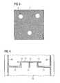
- the present inventionrelates to a wafer handling system including a wafer holder and a wafer chuck.
- the wafer holderhas a set of minimum contact wafer support members predefining support member contacting portions on a planar wafer surface of a wafer.
- the wafer chuckhas a wafer support region for supporting the wafer.
- the wafer support regionis constructed for contacting the planar wafer surface.
- the wafer holder and the wafer chuckhave a relative position to each other which includes a distance extending in a horizontal direction.
- the wafer chuckis formed with recesses configured at predefined positions corresponding to the support member contacting portions of the planar wafer surface.
- the rotational position adjusting deviceis for adjusting a rotational position of the wafer, which is being transported, such that the support member contacting portions of the planar wafer surface are located on the recesses of the wafer chuck when the planar wafer surface is contacted by the wafer support region of the wafer chuck.
Landscapes
- Physics & Mathematics (AREA)
- General Physics & Mathematics (AREA)
- Engineering & Computer Science (AREA)
- Condensed Matter Physics & Semiconductors (AREA)
- Manufacturing & Machinery (AREA)
- Computer Hardware Design (AREA)
- Microelectronics & Electronic Packaging (AREA)
- Power Engineering (AREA)
- Container, Conveyance, Adherence, Positioning, Of Wafer (AREA)
- Exposure And Positioning Against Photoresist Photosensitive Materials (AREA)
- Exposure Of Semiconductors, Excluding Electron Or Ion Beam Exposure (AREA)
Abstract
Description
Claims (18)
Applications Claiming Priority (3)
| Application Number | Priority Date | Filing Date | Title |
|---|---|---|---|
| EP01115947.2 | 2001-06-29 | ||
| EP01115947 | 2001-06-29 | ||
| EP01115947AEP1274121A1 (en) | 2001-06-29 | 2001-06-29 | Wafer chuck for supporting a semiconductor wafer |
Publications (2)
| Publication Number | Publication Date |
|---|---|
| US20030002973A1 US20030002973A1 (en) | 2003-01-02 |
| US6767170B2true US6767170B2 (en) | 2004-07-27 |
Family
ID=8177905
Family Applications (1)
| Application Number | Title | Priority Date | Filing Date |
|---|---|---|---|
| US10/186,970Expired - Fee RelatedUS6767170B2 (en) | 2001-06-29 | 2002-07-01 | Wafer handling system and wafer handling method |
Country Status (3)
| Country | Link |
|---|---|
| US (1) | US6767170B2 (en) |
| EP (1) | EP1274121A1 (en) |
| JP (1) | JP2003092258A (en) |
Cited By (9)
| Publication number | Priority date | Publication date | Assignee | Title |
|---|---|---|---|---|
| US20050106834A1 (en)* | 2003-11-03 | 2005-05-19 | Andry Paul S. | Method and apparatus for filling vias |
| US20070252970A1 (en)* | 2004-09-01 | 2007-11-01 | Nikon Corporation | Substrate Holder, Stage Apparatus, and Exposure Apparatus |
| US20080187416A1 (en)* | 2002-02-25 | 2008-08-07 | Tsutomu Hiroki | Semiconductor processing system |
| US20080227374A1 (en)* | 2007-03-15 | 2008-09-18 | Applied Materials, Inc. | Polishing head testing with movable pedestal |
| US7988399B2 (en) | 2003-11-10 | 2011-08-02 | Brooks Automation, Inc. | Mid-entry load lock for semiconductor handling system |
| US8500388B2 (en) | 2003-11-10 | 2013-08-06 | Brooks Automation, Inc. | Semiconductor wafer handling and transport |
| US9829806B2 (en) | 2014-03-14 | 2017-11-28 | Taiwan Semiconductor Manufacturing Company Limited | Lithography tool with backside polisher |
| US10086511B2 (en) | 2003-11-10 | 2018-10-02 | Brooks Automation, Inc. | Semiconductor manufacturing systems |
| US20240339353A1 (en)* | 2021-08-06 | 2024-10-10 | Beijing Naura Microelectronics Equipment Co., Ltd. | Wafer cleaning equipment, wafer chuck, and wafer cleaning method |
Families Citing this family (5)
| Publication number | Priority date | Publication date | Assignee | Title |
|---|---|---|---|---|
| GB2414858A (en)* | 2004-06-03 | 2005-12-07 | Nanobeam Ltd | A workpiece or specimen support assembly for a charged particle beam system |
| FR3073081B1 (en)* | 2017-10-27 | 2019-11-22 | Commissariat A L'energie Atomique Et Aux Energies Alternatives | SEMICONDUCTOR SUBSTRATE PROTECTED FOR TRANSPORT AND HANDLING |
| US11515191B2 (en)* | 2018-10-26 | 2022-11-29 | Applied Materials, Inc. | Graded dimple height pattern on heater for lower backside damage and low chucking voltage |
| CN113169110A (en)* | 2018-12-14 | 2021-07-23 | 应用材料公司 | Handling and handling of double-sided devices on fragile substrates |
| US12046495B2 (en) | 2020-06-26 | 2024-07-23 | Globalwafers Co., Ltd. | Wafer boats for supporting semiconductor wafers in a furnace |
Citations (28)
| Publication number | Priority date | Publication date | Assignee | Title |
|---|---|---|---|---|
| US4525852A (en)* | 1983-03-15 | 1985-06-25 | Micronix Partners | Alignment apparatus |
| US4582191A (en)* | 1982-06-17 | 1986-04-15 | Weigand Robert E | Article handling apparatus and method |
| US5060354A (en) | 1990-07-02 | 1991-10-29 | George Chizinsky | Heated plate rapid thermal processor |
| US5352249A (en)* | 1992-08-28 | 1994-10-04 | Hughes Aircraft Company | Apparatus for providing consistent, non-jamming registration of semiconductor wafers |
| US5405518A (en) | 1994-04-26 | 1995-04-11 | Industrial Technology Research Institute | Workpiece holder apparatus |
| US5479108A (en)* | 1992-11-25 | 1995-12-26 | David Cheng | Method and apparatus for handling wafers |
| US5695568A (en) | 1993-04-05 | 1997-12-09 | Applied Materials, Inc. | Chemical vapor deposition chamber |
| US5703493A (en) | 1995-10-25 | 1997-12-30 | Motorola, Inc. | Wafer holder for semiconductor applications |
| US5783834A (en)* | 1997-02-20 | 1998-07-21 | Modular Process Technology | Method and process for automatic training of precise spatial locations to a robot |
| US5810935A (en)* | 1994-12-06 | 1998-09-22 | Electronics And Telecommunications Research Institute | Apparatus for transferring a wafer |
| US5842825A (en)* | 1997-10-07 | 1998-12-01 | International Business Machines Corporation | Incremented rotated wafer placement on electro-static chucks for metal etch |
| US5903428A (en)* | 1997-09-25 | 1999-05-11 | Applied Materials, Inc. | Hybrid Johnsen-Rahbek electrostatic chuck having highly resistive mesas separating the chuck from a wafer supported thereupon and method of fabricating same |
| US5974682A (en)* | 1996-09-02 | 1999-11-02 | Tokyo Electron Limited | Cooling process system |
| US6002840A (en)* | 1997-09-30 | 1999-12-14 | Brooks Automation Inc. | Substrate transport apparatus |
| US6007635A (en) | 1997-11-26 | 1999-12-28 | Micro C Technologies, Inc. | Platform for supporting a semiconductor substrate and method of supporting a substrate during rapid high temperature processing |
| US6047480A (en)* | 1998-04-13 | 2000-04-11 | Motorola, Inc. | Method of processing a semiconductor device |
| US6139251A (en)* | 1998-10-17 | 2000-10-31 | Nanya Technology Corporation | Stepper alignment method and apparatus |
| US6151447A (en) | 1993-01-21 | 2000-11-21 | Moore Technologies | Rapid thermal processing apparatus for processing semiconductor wafers |
| US6164894A (en)* | 1997-11-04 | 2000-12-26 | Cheng; David | Method and apparatus for integrated wafer handling and testing |
| US6167893B1 (en)* | 1999-02-09 | 2001-01-02 | Novellus Systems, Inc. | Dynamic chuck for semiconductor wafer or other substrate |
| US6183189B1 (en)* | 1998-11-27 | 2001-02-06 | Chartered Semiconductor Manufacturing, Ltd. | Self aligning wafer chuck design for wafer processing tools |
| US6217663B1 (en) | 1996-06-21 | 2001-04-17 | Kokusai Electric Co., Ltd. | Substrate processing apparatus and substrate processing method |
| US6317647B1 (en)* | 1998-05-20 | 2001-11-13 | Tokyo Electron Limited | Aligner |
| US6318947B1 (en)* | 1999-01-22 | 2001-11-20 | Rite-Hite Holding Corporation | Pulling-style restraint for a parked swap body |
| US6425280B1 (en)* | 1999-07-30 | 2002-07-30 | International Business Machines Corporation | Wafer alignment jig for wafer-handling systems |
| US6478532B1 (en)* | 1999-11-30 | 2002-11-12 | Asyst Technologies, Inc. | Wafer orienting and reading mechanism |
| US6537143B1 (en)* | 1999-06-22 | 2003-03-25 | Samsung Electronics Co., Ltd. | Pedestal of a load-cup which supports wafers loaded/unloaded onto/from a chemical mechanical polishing apparatus |
| US6601313B2 (en)* | 2001-02-05 | 2003-08-05 | Samsung Electronics Co., Ltd. | System and method for detecting position of semiconductor wafer |
- 2001
- 2001-06-29EPEP01115947Apatent/EP1274121A1/ennot_activeWithdrawn
- 2002
- 2002-06-21JPJP2002182235Apatent/JP2003092258A/enactivePending
- 2002-07-01USUS10/186,970patent/US6767170B2/ennot_activeExpired - Fee Related
Patent Citations (28)
| Publication number | Priority date | Publication date | Assignee | Title |
|---|---|---|---|---|
| US4582191A (en)* | 1982-06-17 | 1986-04-15 | Weigand Robert E | Article handling apparatus and method |
| US4525852A (en)* | 1983-03-15 | 1985-06-25 | Micronix Partners | Alignment apparatus |
| US5060354A (en) | 1990-07-02 | 1991-10-29 | George Chizinsky | Heated plate rapid thermal processor |
| US5352249A (en)* | 1992-08-28 | 1994-10-04 | Hughes Aircraft Company | Apparatus for providing consistent, non-jamming registration of semiconductor wafers |
| US5479108A (en)* | 1992-11-25 | 1995-12-26 | David Cheng | Method and apparatus for handling wafers |
| US6151447A (en) | 1993-01-21 | 2000-11-21 | Moore Technologies | Rapid thermal processing apparatus for processing semiconductor wafers |
| US5695568A (en) | 1993-04-05 | 1997-12-09 | Applied Materials, Inc. | Chemical vapor deposition chamber |
| US5405518A (en) | 1994-04-26 | 1995-04-11 | Industrial Technology Research Institute | Workpiece holder apparatus |
| US5810935A (en)* | 1994-12-06 | 1998-09-22 | Electronics And Telecommunications Research Institute | Apparatus for transferring a wafer |
| US5703493A (en) | 1995-10-25 | 1997-12-30 | Motorola, Inc. | Wafer holder for semiconductor applications |
| US6217663B1 (en) | 1996-06-21 | 2001-04-17 | Kokusai Electric Co., Ltd. | Substrate processing apparatus and substrate processing method |
| US5974682A (en)* | 1996-09-02 | 1999-11-02 | Tokyo Electron Limited | Cooling process system |
| US5783834A (en)* | 1997-02-20 | 1998-07-21 | Modular Process Technology | Method and process for automatic training of precise spatial locations to a robot |
| US5903428A (en)* | 1997-09-25 | 1999-05-11 | Applied Materials, Inc. | Hybrid Johnsen-Rahbek electrostatic chuck having highly resistive mesas separating the chuck from a wafer supported thereupon and method of fabricating same |
| US6002840A (en)* | 1997-09-30 | 1999-12-14 | Brooks Automation Inc. | Substrate transport apparatus |
| US5842825A (en)* | 1997-10-07 | 1998-12-01 | International Business Machines Corporation | Incremented rotated wafer placement on electro-static chucks for metal etch |
| US6164894A (en)* | 1997-11-04 | 2000-12-26 | Cheng; David | Method and apparatus for integrated wafer handling and testing |
| US6007635A (en) | 1997-11-26 | 1999-12-28 | Micro C Technologies, Inc. | Platform for supporting a semiconductor substrate and method of supporting a substrate during rapid high temperature processing |
| US6047480A (en)* | 1998-04-13 | 2000-04-11 | Motorola, Inc. | Method of processing a semiconductor device |
| US6317647B1 (en)* | 1998-05-20 | 2001-11-13 | Tokyo Electron Limited | Aligner |
| US6139251A (en)* | 1998-10-17 | 2000-10-31 | Nanya Technology Corporation | Stepper alignment method and apparatus |
| US6183189B1 (en)* | 1998-11-27 | 2001-02-06 | Chartered Semiconductor Manufacturing, Ltd. | Self aligning wafer chuck design for wafer processing tools |
| US6318947B1 (en)* | 1999-01-22 | 2001-11-20 | Rite-Hite Holding Corporation | Pulling-style restraint for a parked swap body |
| US6167893B1 (en)* | 1999-02-09 | 2001-01-02 | Novellus Systems, Inc. | Dynamic chuck for semiconductor wafer or other substrate |
| US6537143B1 (en)* | 1999-06-22 | 2003-03-25 | Samsung Electronics Co., Ltd. | Pedestal of a load-cup which supports wafers loaded/unloaded onto/from a chemical mechanical polishing apparatus |
| US6425280B1 (en)* | 1999-07-30 | 2002-07-30 | International Business Machines Corporation | Wafer alignment jig for wafer-handling systems |
| US6478532B1 (en)* | 1999-11-30 | 2002-11-12 | Asyst Technologies, Inc. | Wafer orienting and reading mechanism |
| US6601313B2 (en)* | 2001-02-05 | 2003-08-05 | Samsung Electronics Co., Ltd. | System and method for detecting position of semiconductor wafer |
Cited By (18)
| Publication number | Priority date | Publication date | Assignee | Title |
|---|---|---|---|---|
| US20080187416A1 (en)* | 2002-02-25 | 2008-08-07 | Tsutomu Hiroki | Semiconductor processing system |
| US7857569B2 (en)* | 2002-02-25 | 2010-12-28 | Tokyo Electron Limited | Semiconductor processing system |
| US7449067B2 (en)* | 2003-11-03 | 2008-11-11 | International Business Machines Corporation | Method and apparatus for filling vias |
| US20050106834A1 (en)* | 2003-11-03 | 2005-05-19 | Andry Paul S. | Method and apparatus for filling vias |
| US8672605B2 (en) | 2003-11-10 | 2014-03-18 | Brooks Automation, Inc. | Semiconductor wafer handling and transport |
| US10086511B2 (en) | 2003-11-10 | 2018-10-02 | Brooks Automation, Inc. | Semiconductor manufacturing systems |
| US9884726B2 (en) | 2003-11-10 | 2018-02-06 | Brooks Automation, Inc. | Semiconductor wafer handling transport |
| US7988399B2 (en) | 2003-11-10 | 2011-08-02 | Brooks Automation, Inc. | Mid-entry load lock for semiconductor handling system |
| US8500388B2 (en) | 2003-11-10 | 2013-08-06 | Brooks Automation, Inc. | Semiconductor wafer handling and transport |
| US20070252970A1 (en)* | 2004-09-01 | 2007-11-01 | Nikon Corporation | Substrate Holder, Stage Apparatus, and Exposure Apparatus |
| US20100141924A1 (en)* | 2004-09-01 | 2010-06-10 | Nikon Corporation | Substrate holder, stage apparatus, and exposure apparatus with first support part provided in a suction space and second support part |
| US8717543B2 (en) | 2004-09-01 | 2014-05-06 | Nikon Corporation | Substrate holder, stage apparatus, and exposure apparatus with first support part provided in a suction space and second support part |
| US20100327900A1 (en)* | 2007-03-15 | 2010-12-30 | Applied Materials, Inc. | Polishing head testing with movable pedestal |
| US8008941B2 (en) | 2007-03-15 | 2011-08-30 | Applied Materials, Inc. | Polishing head testing with movable pedestal |
| US20080227374A1 (en)* | 2007-03-15 | 2008-09-18 | Applied Materials, Inc. | Polishing head testing with movable pedestal |
| US7750657B2 (en) | 2007-03-15 | 2010-07-06 | Applied Materials Inc. | Polishing head testing with movable pedestal |
| US9829806B2 (en) | 2014-03-14 | 2017-11-28 | Taiwan Semiconductor Manufacturing Company Limited | Lithography tool with backside polisher |
| US20240339353A1 (en)* | 2021-08-06 | 2024-10-10 | Beijing Naura Microelectronics Equipment Co., Ltd. | Wafer cleaning equipment, wafer chuck, and wafer cleaning method |
Also Published As
| Publication number | Publication date |
|---|---|
| US20030002973A1 (en) | 2003-01-02 |
| JP2003092258A (en) | 2003-03-28 |
| EP1274121A1 (en) | 2003-01-08 |
Similar Documents
| Publication | Publication Date | Title |
|---|---|---|
| US6767170B2 (en) | Wafer handling system and wafer handling method | |
| TWI778133B (en) | In-situ apparatus for semiconductor process module | |
| US5609689A (en) | Vacuum process apparaus | |
| KR102010720B1 (en) | Substrate processing apparatus and substrate processing method | |
| US6361313B1 (en) | Ladder boat for supporting wafers | |
| KR100550755B1 (en) | Substrate holding device | |
| TWI439557B (en) | Workpiece rotation apparatus for a plasma reactor system | |
| KR101728390B1 (en) | Etching device and plasma processing device | |
| US6183189B1 (en) | Self aligning wafer chuck design for wafer processing tools | |
| TW202239532A (en) | Minimal contact retention of thin optical devices | |
| KR20250036427A (en) | A ring assembly for a semiconductor process, a substrate processing apparatus including the same, and a method of manufacturing a semiconductor device using the same | |
| JP2001326267A (en) | Semiconductor processing apparatus | |
| JPH06132387A (en) | Vacuum adsorption stage | |
| JP2005223142A (en) | Substrate holder, film formation processing apparatus, and processing apparatus | |
| JP3098809B2 (en) | Wafer processing method | |
| JPH09289173A (en) | Vertical thermal treatment equipment | |
| JP2025518491A (en) | Edge ring system and corresponding middle ring, edge ring, moving ring, stationary ring and bottom ring | |
| US20020124964A1 (en) | Wafer support plate assembly having recessed upper pad and vacuum processing apparatus comprising the same | |
| JPH09232413A (en) | Semiconductor manufacturing equipment having a wafer loading stage | |
| KR20010102302A (en) | Film forming device | |
| KR20010051372A (en) | Wafer processing apparatus | |
| JP3323168B2 (en) | Semiconductor manufacturing equipment | |
| KR200192643Y1 (en) | Wafer table of cool down chamber | |
| US12412773B2 (en) | Vacuum chuck | |
| KR102297311B1 (en) | Assembly for supporting substrate and apparatus for processing having the same |
Legal Events
| Date | Code | Title | Description |
|---|---|---|---|
| FEPP | Fee payment procedure | Free format text:PAYOR NUMBER ASSIGNED (ORIGINAL EVENT CODE: ASPN); ENTITY STATUS OF PATENT OWNER: LARGE ENTITY Free format text:PAYER NUMBER DE-ASSIGNED (ORIGINAL EVENT CODE: RMPN); ENTITY STATUS OF PATENT OWNER: LARGE ENTITY | |
| AS | Assignment | Owner name:INFINEON TECHNOLOGIES SC300 GMBH & CO. KG, GERMANY Free format text:ASSIGNMENT OF ASSIGNORS INTEREST;ASSIGNORS:KOSTLER, WOLFRAM;HRASCHAN, GUNTHER;REEL/FRAME:015202/0237;SIGNING DATES FROM 20020813 TO 20030115 | |
| FPAY | Fee payment | Year of fee payment:4 | |
| AS | Assignment | Owner name:QIMONDA AG, GERMANY Free format text:ASSIGNMENT OF ASSIGNORS INTEREST;ASSIGNOR:INFINEON TECHNOLOGIES SC300 GMBH & CO. KG;REEL/FRAME:023854/0001 Effective date:20060425 | |
| FPAY | Fee payment | Year of fee payment:8 | |
| AS | Assignment | Owner name:INFINEON TECHNOLOGIES AG, GERMANY Free format text:ASSIGNMENT OF ASSIGNORS INTEREST;ASSIGNOR:QIMONDA AG;REEL/FRAME:035623/0001 Effective date:20141009 | |
| AS | Assignment | Owner name:POLARIS INNOVATIONS LIMITED, IRELAND Free format text:ASSIGNMENT OF ASSIGNORS INTEREST;ASSIGNOR:INFINEON TECHNOLOGIES AG;REEL/FRAME:036723/0021 Effective date:20150708 | |
| REMI | Maintenance fee reminder mailed | ||
| LAPS | Lapse for failure to pay maintenance fees | ||
| STCH | Information on status: patent discontinuation | Free format text:PATENT EXPIRED DUE TO NONPAYMENT OF MAINTENANCE FEES UNDER 37 CFR 1.362 | |
| FP | Lapsed due to failure to pay maintenance fee | Effective date:20160727 |