US6765828B2 - Non-volatile semiconductor storage device and method of reading out data - Google Patents
Non-volatile semiconductor storage device and method of reading out dataDownload PDFInfo
- Publication number
- US6765828B2 US6765828B2US10/356,496US35649603AUS6765828B2US 6765828 B2US6765828 B2US 6765828B2US 35649603 AUS35649603 AUS 35649603AUS 6765828 B2US6765828 B2US 6765828B2
- Authority
- US
- United States
- Prior art keywords
- source line
- capacitor
- memory cell
- storage device
- semiconductor storage
- Prior art date
- Legal status (The legal status is an assumption and is not a legal conclusion. Google has not performed a legal analysis and makes no representation as to the accuracy of the status listed.)
- Expired - Lifetime
Links
Images


Classifications
- G—PHYSICS
- G11—INFORMATION STORAGE
- G11C—STATIC STORES
- G11C16/00—Erasable programmable read-only memories
- G11C16/02—Erasable programmable read-only memories electrically programmable
- G11C16/06—Auxiliary circuits, e.g. for writing into memory
- G11C16/26—Sensing or reading circuits; Data output circuits
- G—PHYSICS
- G11—INFORMATION STORAGE
- G11C—STATIC STORES
- G11C16/00—Erasable programmable read-only memories
- G11C16/02—Erasable programmable read-only memories electrically programmable
- G11C16/06—Auxiliary circuits, e.g. for writing into memory
- G11C16/30—Power supply circuits
- G—PHYSICS
- G11—INFORMATION STORAGE
- G11C—STATIC STORES
- G11C16/00—Erasable programmable read-only memories
- G11C16/02—Erasable programmable read-only memories electrically programmable
- G11C16/06—Auxiliary circuits, e.g. for writing into memory
- G11C16/26—Sensing or reading circuits; Data output circuits
- G11C16/28—Sensing or reading circuits; Data output circuits using differential sensing or reference cells, e.g. dummy cells
Definitions
- the present inventionrelates to non-volatile semiconductor storage devices, in particular to a non-volatile semiconductor storage device operating under a method of reading out data from a cell of the virtual ground type, and a method of reading out data.
- the virtual ground typeis known as a way to achieve a large capacity memory.
- the virtual ground typeincreases the density of the cells by reducing the number of contacts of the cell and thus is suitable for a large capacity memory.
- the method of reading out data from the cellbecomes more complex and thus is not suitable for a low voltage and high-speed memory.
- a method(hereinafter also referred to as the first conventional method) of pre-charging all of the bit lines to cancel out the leak current from the adjacent cells and then detecting the level or the current on the side of the drain; and a method (hereinafter also referred to as the second conventional method) of detecting the level on the side of the source where the influence of the leak current of the cells is smaller, are used.
- the second conventional methodis disclosed in, for example, Japanese Laid-Open Patent Application 3-176895.
- the non-volatile storage device of the present inventionis a non-volatile semiconductor storage device provided with a boost circuit for setting, for at least a certain period of time, a source line selectively connected to a memory cell to a negative potential, when reading out data from the memory cell.
- the reading marginis the difference between such negative potential and the positive potential and an extended reading margin can be obtained. Even at the time of low-voltage operation, the reading margin can reliably sense the change in the potential of the source line because the negative voltage is set as the reference voltage.
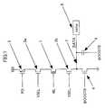
- FIG. 1is a circuit diagram showing the principle of the present invention
- FIG. 2is a wave form chart showing the principle of the present invention and operations according to one embodiment of the present invention.
- FIG. 3is a circuit diagram showing a non-volatile semiconductor storage device according to one embodiment of the present invention.
- FIG. 1is a circuit diagram showing the principle of the present invention.
- FIG. 1shows one memory cell 1 and a circuit construction around such memory cell 1 .
- the memory cell 1is a non-volatile transistor that is electrically programmable and electrically erasable.
- the memory cell 1includes a source, a drain, a control gate, and a floating gate.
- the drain of the memory cell 1is connected to a positive supply voltage VCC via a transistor 2 a of Y decoder and a transistor 3 of a load part.
- the transistor 3is turned on when receiving a low-level load signal PD.
- the transistor 2 ais turned on when receiving a high-level select signal YSEL.
- the memory cell 1is turned on when receiving a high-level word line drive signal WL.
- the source of the memory cell 1(connected to the bit line) is grounded via a transistor 2 b of Y decoder and a transistor 4 for discharging the source line.
- the connecting point of the transistor 2 b and the transistor 4is connected to a source line 7 that is in turn connected to a sense amplifier (samp) 5 .
- the transistor 2 bis turned on when receiving a high-level select signal YSEL.
- the transistor 4is turned on when receiving a high-level boost signal BOOSTB. In other words, the bit line leading to the memory cell 1 is selectively grounded (virtual ground).
- a capacitor 6for boosting the source line 7 to a negative potential, is connected.
- the other end of the capacitor 6is supplied with a boost signal BOOSTB.
- One feature of the circuit shown in FIG. 1is that the transistor 4 and the capacitor 6 are provided, so that the source line 7 can be boosted to a negative potential when reading data out from the memory cell 1 . Thus, the margin necessary for reading can be sufficiently ensured.
- FIG. 2shows a wave form chart showing the operation of the circuit shown in FIG. 1 .
- the boost signal BOOSTBrises from 0V (ground level) to the supply voltage VCC at the beginning of the reading operation.
- the boost signal BOOSTBcorresponds to, for example, a signal generated when a change in address is detected.
- the transistor 4is turned on and the potential of the source line 7 is securely set to 0V (FIG. 2 ( a )). Hence, the capacitor 6 starts to be charged.
- one bit lineis selected by the address after the change. If the memory cell 1 in FIG. 1 is selected, the select signal YSEL rises to the supply voltage VCC thus turning on the transistors 2 a and 2 b , and similarly, the word line WL rises to the supply voltage VCC (FIG. 2 ( b )) thus turning on the memory cell 1 . At this point, the load signal PD of the bit line is at the supply voltage (OFF state).
- the boost signal BOOSTBfalls to 0V.
- the boost signal BOOSTBis a pulse-form signal that rises to the supply voltage VCC only for a defined period of time. The moment the boost signal BOOSTB falls to 0V, the potential of the source line 7 decreases by the amount of voltage between the ends of the capacitor 6 and becomes a negative potential V_ (FIG. 2 ( a )). In other words, the source line 7 is boosted to the negative potential V_.
- the load signal PDfalls from the supply voltage VCC to 0V (FIG. 2 ( d )) and the transistor 3 is turned on.
- the source line 7when data is not written into the memory cell 1 (data bit “ 1 ”), or when in the erase state, the source line 7 is charged. In other words, the current flows from the supply voltage VCC, through the transistors 3 , 2 a , 1 , and 2 b , into the source line 7 , and then out through the capacitor 6 to the ground. Thus, the potential of the source line 7 gradually rises from the negative potential V_, beyond the ground level (0V) to a certain positive potential towards the supply voltage VCC (DATA “ 1 ” of FIG. 2 ( a )).
- Such positive potentialis a value derived by subtracting the sum of the threshold voltages of the transistors 3 , 2 a , 1 , and 2 b from the supply voltage VCC.
- DATA “ 0 ” and DATA “ 1 ”become the reading margins.
- DATA “ 0 ” and DATA “ 1 ”can be distinguished by setting the threshold value ref for reading between such reading margins.
- the conventional constructionis a circuit construction in which the transistor 4 and the capacitor 6 of FIG. 1 are not provided.
- the potential of the DATA “ 0 ”is the ground level of 0V.
- the reading marginis smaller than the present invention by the amount (0V-V_).
- the reading marginbecomes smaller by having the negative voltage V_ as the reference voltage, it is still possible to ensure sufficient margins.
- the influence of the leak current of the adjacent memory cellsis small.
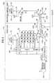
- FIG. 3is a block diagram showing an overall construction of the non-volatile semiconductor storage device according to the embodiment of the present invention.
- the non-volatile semiconductor storage device shown in the figureincludes a core part 100 and a reference circuit part 200 .
- the core part 100includes a storing section for storing the actual data
- the reference circuit part 200includes a section for setting and outputting the threshold value ref explained above.
- the core part 100includes a memory cell array 20 , an address buffer 21 , an ATD (Address Transition Detection) circuit 22 , an X decoder (X-DEC) 23 , Y decoders (Y-DEC) 24 A, 24 B, a load circuit 25 , a sense amplifier (S/A) 26 , transistors 27 - 34 , and a capacitor 35 . Furthermore, reference number 36 denotes a source line.
- the transistor 33 of FIG. 3corresponds to the transistor 4 of FIG. 1, and the capacitor 35 of FIG. 3 corresponds to the capacitor 6 of FIG. 1 .
- the ATD signal output from the ATD circuit 22 of FIG. 3corresponds to the boost signal BOOSTB in FIG. 1 .
- the load circuit 25 of FIG. 3corresponds to the transistor 3 of FIG. 1 and the transistors 27 - 29 correspond to the transistor 2 a of FIG. 1 .
- the transistors 30 - 32 of FIG. 3correspond to the transistor 2 b of FIG. 1, and one of the memory cell transistors of the memory cell array 20 of FIG. 3 corresponds to the memory cell 1 of FIG. 1 .
- the sense amplifier 26 of FIG. 3corresponds to the sense amplifier 5 of FIG. 1 .
- the reference circuit part 200includes a load circuit 50 , transistors 51 , 52 , 54 - 56 , a memory cell transistor 53 , and a capacitor 57 .
- reference number 58denotes a source line.
- the transistors 51 and 52correspond to the transistors 27 and 28 ( 29 ) of the core part 100
- the transistors 54 and 55correspond to the transistors 30 ( 31 ) and 32 of core part 100
- the capacitor 57corresponds to the capacitor 35 of the core part 100
- the transistor 56corresponds to the transistor 33 of the core part 100 .
- the supply voltage VCCis applied to the gates of the transistors 51 , 52 , 54 , and 55 .
- transistors 33 , 56 , and capacitors 35 , 57are newly provided.
- the transistor 33 and the capacitor 35form the boost circuit for the source line 36 of the core part 100 .
- the transistor 56 and the capacitor 57form the boost circuit for the source line 58 of the reference circuit part 200 .
- the transistor 33 and the capacitor 35are similar to the transistor 4 and the capacitor 6 explained with reference to FIG. 1 .
- the transistor 56 and the capacitor 57are provided in the reference circuit part 200 .
- the external address signal Addis buffered in the address buffer 21 and then output to the ATD circuit 22 as well as to the X decoder 23 and the Y decoders 24 A, 24 B.
- the ATD circuit 22generates the ATD signal when detecting change in the address signal Add (FIG. 2 (C)).
- the ATD signalis provided to the transistors 33 , 34 , 56 , and to the capacitors 35 , 57 .
- the source lines 36 and 58are short-circuited and simultaneously set to the ground level (0V).
- the X decoder 23decodes the address signal Add and selects one word line. Furthermore, the X decoder 23 outputs the select signal REF_WL to the control gate of the memory cell 53 on the side of the reference circuit part 200 each time it decodes the address signal Add (FIG. 2 ( b )).
- the Y decoder 24 Adecodes the address signal Add and turns on the transistor 27 and transistor 28 or 29 . Similarly, the Y decoder 24 B decodes the address signal Add and turns on the transistor 32 and the transistor 30 or 31 . Thus, one of the memory cells of the memory cell array 20 and the memory cell 53 on the side of the reference circuit part 200 are selected.
- the ATD signalthen falls (FIG. 2 ( c )).
- the transistors 33 , 56 and 34are turned off.
- the source line 36 of the core part 100is set to a negative potential, as mentioned above.
- the source line 58 of the reference circuit part 200is set to a negative potential.
- the load signal PDfalls from the supply voltage VCC to the ground level (FIG. 2 ( d )).
- the supply voltage VCCis supplied from the load circuit 25 , 50 to the transistors 27 , 51 , respectively.
- the selected memory cellstores DATA “ 1 ”
- the currentflows from the load circuit 25 , and passes through the transistors 27 , 28 (or 29 ), the selected memory cell, the transistor 30 (or 31 ), the transistor 32 , and the capacitor 35 .
- the potential of the source line 36rises above the ground level to a positive potential, as shown in FIG. 2 ( a ). If the selected memory cell stores DATA “ 0 ”, the level of the source line 36 remains to be a negative potential V_.
- the source line 58 of the reference circuit part 200rises when the ATD signal falls to 0V and the load signal falls to 0V, as with the ref in FIG. 2 ( a ).
- the threshold value refis an arbitrary potential set between the DATA “ 0 ” and the DATA “ 1 ”.
- the reference potential refpasses through the source line 58 and is applied to the sense amplifier 26 , as DATAR.
- the sense amplifier 26compares the data DATA read out from the selected memory cell and the threshold value DATAR, and outputs the comparison result as the sense amplifier output signal SAOUT. In other words, the sense amplifier 26 compares the potential of the source line 36 and the potential of the source line 58 , and outputs the sense amplifier SAOUT according to the magnitude relation of such comparison.
- the margin for readingcan be extended, and can respond to the low operating voltage.
- the writing and erasing operationsare those generally known. Furthermore, the internal construction of the address buffer 21 , the ATD circuit 22 , the X decoder 23 , the Y decoders 24 A, 24 B, the load circuits 25 , 50 and the sense amplifier 26 are also those generally known.
- the boost circuit including the capacitor 35 and the transistor 33can be replaced by another circuit having a similar function.
- the transistor 34short-circuits both the source line 36 and 58 to set the source lines to the ground level, the transistor 34 may be omitted.
Landscapes
- Read Only Memory (AREA)
Abstract
Description
Claims (8)
Applications Claiming Priority (1)
| Application Number | Priority Date | Filing Date | Title |
|---|---|---|---|
| PCT/JP2000/005223WO2002013199A1 (en) | 2000-08-03 | 2000-08-03 | Nonvolatile semiconductor memory and method of reading data |
Related Parent Applications (1)
| Application Number | Title | Priority Date | Filing Date |
|---|---|---|---|
| PCT/JP2000/005223ContinuationWO2002013199A1 (en) | 2000-08-03 | 2000-08-03 | Nonvolatile semiconductor memory and method of reading data |
Publications (2)
| Publication Number | Publication Date |
|---|---|
| US20030117841A1 US20030117841A1 (en) | 2003-06-26 |
| US6765828B2true US6765828B2 (en) | 2004-07-20 |
Family
ID=11736324
Family Applications (1)
| Application Number | Title | Priority Date | Filing Date |
|---|---|---|---|
| US10/356,496Expired - LifetimeUS6765828B2 (en) | 2000-08-03 | 2003-02-03 | Non-volatile semiconductor storage device and method of reading out data |
Country Status (4)
| Country | Link |
|---|---|
| US (1) | US6765828B2 (en) |
| JP (1) | JP4579493B2 (en) |
| KR (1) | KR100597060B1 (en) |
| WO (1) | WO2002013199A1 (en) |
Cited By (2)
| Publication number | Priority date | Publication date | Assignee | Title |
|---|---|---|---|---|
| US20050083764A1 (en)* | 2003-10-15 | 2005-04-21 | Oki Electric Industry Co., Ltd. | Semiconductor integrated circuit |
| US8320188B2 (en) | 2010-07-28 | 2012-11-27 | SK Hynix Inc. | Semiconductor apparatus and method for transferring control voltage |
Families Citing this family (37)
| Publication number | Priority date | Publication date | Assignee | Title |
|---|---|---|---|---|
| US6768165B1 (en) | 1997-08-01 | 2004-07-27 | Saifun Semiconductors Ltd. | Two bit non-volatile electrically erasable and programmable semiconductor memory cell utilizing asymmetrical charge trapping |
| US6614692B2 (en) | 2001-01-18 | 2003-09-02 | Saifun Semiconductors Ltd. | EEPROM array and method for operation thereof |
| US6584017B2 (en) | 2001-04-05 | 2003-06-24 | Saifun Semiconductors Ltd. | Method for programming a reference cell |
| US6700818B2 (en) | 2002-01-31 | 2004-03-02 | Saifun Semiconductors Ltd. | Method for operating a memory device |
| US6917544B2 (en) | 2002-07-10 | 2005-07-12 | Saifun Semiconductors Ltd. | Multiple use memory chip |
| US6963505B2 (en)* | 2002-10-29 | 2005-11-08 | Aifun Semiconductors Ltd. | Method circuit and system for determining a reference voltage |
| US7136304B2 (en) | 2002-10-29 | 2006-11-14 | Saifun Semiconductor Ltd | Method, system and circuit for programming a non-volatile memory array |
| US6992932B2 (en) | 2002-10-29 | 2006-01-31 | Saifun Semiconductors Ltd | Method circuit and system for read error detection in a non-volatile memory array |
| US6967896B2 (en)* | 2003-01-30 | 2005-11-22 | Saifun Semiconductors Ltd | Address scramble |
| US7178004B2 (en) | 2003-01-31 | 2007-02-13 | Yan Polansky | Memory array programming circuit and a method for using the circuit |
| US7142464B2 (en) | 2003-04-29 | 2006-11-28 | Saifun Semiconductors Ltd. | Apparatus and methods for multi-level sensing in a memory array |
| US7123532B2 (en) | 2003-09-16 | 2006-10-17 | Saifun Semiconductors Ltd. | Operating array cells with matched reference cells |
| WO2005094178A2 (en) | 2004-04-01 | 2005-10-13 | Saifun Semiconductors Ltd. | Method, circuit and systems for erasing one or more non-volatile memory cells |
| US7755938B2 (en)* | 2004-04-19 | 2010-07-13 | Saifun Semiconductors Ltd. | Method for reading a memory array with neighbor effect cancellation |
| US7317633B2 (en) | 2004-07-06 | 2008-01-08 | Saifun Semiconductors Ltd | Protection of NROM devices from charge damage |
| US7095655B2 (en)* | 2004-08-12 | 2006-08-22 | Saifun Semiconductors Ltd. | Dynamic matching of signal path and reference path for sensing |
| US20060036803A1 (en)* | 2004-08-16 | 2006-02-16 | Mori Edan | Non-volatile memory device controlled by a micro-controller |
| US7638850B2 (en) | 2004-10-14 | 2009-12-29 | Saifun Semiconductors Ltd. | Non-volatile memory structure and method of fabrication |
| US7257025B2 (en)* | 2004-12-09 | 2007-08-14 | Saifun Semiconductors Ltd | Method for reading non-volatile memory cells |
| US7535765B2 (en) | 2004-12-09 | 2009-05-19 | Saifun Semiconductors Ltd. | Non-volatile memory device and method for reading cells |
| EP1686592A3 (en) | 2005-01-19 | 2007-04-25 | Saifun Semiconductors Ltd. | Partial erase verify |
| JP4338656B2 (en) | 2005-02-15 | 2009-10-07 | 富士通マイクロエレクトロニクス株式会社 | Method for writing semiconductor memory device |
| US8053812B2 (en) | 2005-03-17 | 2011-11-08 | Spansion Israel Ltd | Contact in planar NROM technology |
| US8400841B2 (en) | 2005-06-15 | 2013-03-19 | Spansion Israel Ltd. | Device to program adjacent storage cells of different NROM cells |
| US7184313B2 (en) | 2005-06-17 | 2007-02-27 | Saifun Semiconductors Ltd. | Method circuit and system for compensating for temperature induced margin loss in non-volatile memory cells |
| US7786512B2 (en) | 2005-07-18 | 2010-08-31 | Saifun Semiconductors Ltd. | Dense non-volatile memory array and method of fabrication |
| US7668017B2 (en) | 2005-08-17 | 2010-02-23 | Saifun Semiconductors Ltd. | Method of erasing non-volatile memory cells |
| US7221138B2 (en) | 2005-09-27 | 2007-05-22 | Saifun Semiconductors Ltd | Method and apparatus for measuring charge pump output current |
| JP5065594B2 (en) | 2005-12-23 | 2012-11-07 | 株式会社東芝 | Semiconductor memory device |
| US7352627B2 (en) | 2006-01-03 | 2008-04-01 | Saifon Semiconductors Ltd. | Method, system, and circuit for operating a non-volatile memory array |
| US7808818B2 (en) | 2006-01-12 | 2010-10-05 | Saifun Semiconductors Ltd. | Secondary injection for NROM |
| US7692961B2 (en) | 2006-02-21 | 2010-04-06 | Saifun Semiconductors Ltd. | Method, circuit and device for disturb-control of programming nonvolatile memory cells by hot-hole injection (HHI) and by channel hot-electron (CHE) injection |
| US8253452B2 (en) | 2006-02-21 | 2012-08-28 | Spansion Israel Ltd | Circuit and method for powering up an integrated circuit and an integrated circuit utilizing same |
| US7760554B2 (en) | 2006-02-21 | 2010-07-20 | Saifun Semiconductors Ltd. | NROM non-volatile memory and mode of operation |
| US7638835B2 (en) | 2006-02-28 | 2009-12-29 | Saifun Semiconductors Ltd. | Double density NROM with nitride strips (DDNS) |
| US7701779B2 (en) | 2006-04-27 | 2010-04-20 | Sajfun Semiconductors Ltd. | Method for programming a reference cell |
| US7605579B2 (en) | 2006-09-18 | 2009-10-20 | Saifun Semiconductors Ltd. | Measuring and controlling current consumption and output current of charge pumps |
Citations (10)
| Publication number | Priority date | Publication date | Assignee | Title |
|---|---|---|---|---|
| US5027321A (en) | 1989-11-21 | 1991-06-25 | Intel Corporation | Apparatus and method for improved reading/programming of virtual ground EPROM arrays |
| US5157626A (en)* | 1989-11-21 | 1992-10-20 | Nec Corporation | Semiconductor memory |
| US5457652A (en)* | 1994-04-01 | 1995-10-10 | National Semiconductor Corporation | Low voltage EEPROM |
| JPH09245478A (en) | 1997-01-30 | 1997-09-19 | Oki Electric Ind Co Ltd | Substrate bias generation circuit |
| JPH09246404A (en) | 1996-03-04 | 1997-09-19 | Mitsubishi Electric Corp | Nonvolatile semiconductor memory device |
| US5715191A (en)* | 1995-10-25 | 1998-02-03 | Matsushita Electric Industrial Co., Ltd. | Static random access memory having variable supply voltages to the memory cells and method of operating thereof |
| US5789967A (en)* | 1995-03-31 | 1998-08-04 | Nec Corporation | Semiconductor device with boost voltage supply means |
| US6181629B1 (en)* | 1999-06-23 | 2001-01-30 | Mitsubishi Denki Kabushiki Kaisha | Semiconductor memory device incorporating potential generation circuit with rapid rise of output potential |
| JP3176895B2 (en) | 1998-05-20 | 2001-06-18 | 株式会社日本触媒 | Method for producing α-oxoaldehyde |
| US6249458B1 (en)* | 2000-06-22 | 2001-06-19 | Xilinx, Inc. | Switching circuit for transference of multiple negative voltages |
Family Cites Families (1)
| Publication number | Priority date | Publication date | Assignee | Title |
|---|---|---|---|---|
| JPH09180458A (en)* | 1995-10-25 | 1997-07-11 | Matsushita Electric Ind Co Ltd | Data storage device and driving method thereof |
- 2000
- 2000-08-03JPJP2002518468Apatent/JP4579493B2/ennot_activeExpired - Fee Related
- 2000-08-03WOPCT/JP2000/005223patent/WO2002013199A1/ennot_activeCeased
- 2000-08-03KRKR1020037001343Apatent/KR100597060B1/ennot_activeExpired - Fee Related
- 2003
- 2003-02-03USUS10/356,496patent/US6765828B2/ennot_activeExpired - Lifetime
Patent Citations (11)
| Publication number | Priority date | Publication date | Assignee | Title |
|---|---|---|---|---|
| US5027321A (en) | 1989-11-21 | 1991-06-25 | Intel Corporation | Apparatus and method for improved reading/programming of virtual ground EPROM arrays |
| JPH03176895A (en) | 1989-11-21 | 1991-07-31 | Intel Corp | Method and apparatus for reading and programming virtual grounded eprom array |
| US5157626A (en)* | 1989-11-21 | 1992-10-20 | Nec Corporation | Semiconductor memory |
| US5457652A (en)* | 1994-04-01 | 1995-10-10 | National Semiconductor Corporation | Low voltage EEPROM |
| US5789967A (en)* | 1995-03-31 | 1998-08-04 | Nec Corporation | Semiconductor device with boost voltage supply means |
| US5715191A (en)* | 1995-10-25 | 1998-02-03 | Matsushita Electric Industrial Co., Ltd. | Static random access memory having variable supply voltages to the memory cells and method of operating thereof |
| JPH09246404A (en) | 1996-03-04 | 1997-09-19 | Mitsubishi Electric Corp | Nonvolatile semiconductor memory device |
| JPH09245478A (en) | 1997-01-30 | 1997-09-19 | Oki Electric Ind Co Ltd | Substrate bias generation circuit |
| JP3176895B2 (en) | 1998-05-20 | 2001-06-18 | 株式会社日本触媒 | Method for producing α-oxoaldehyde |
| US6181629B1 (en)* | 1999-06-23 | 2001-01-30 | Mitsubishi Denki Kabushiki Kaisha | Semiconductor memory device incorporating potential generation circuit with rapid rise of output potential |
| US6249458B1 (en)* | 2000-06-22 | 2001-06-19 | Xilinx, Inc. | Switching circuit for transference of multiple negative voltages |
Cited By (3)
| Publication number | Priority date | Publication date | Assignee | Title |
|---|---|---|---|---|
| US20050083764A1 (en)* | 2003-10-15 | 2005-04-21 | Oki Electric Industry Co., Ltd. | Semiconductor integrated circuit |
| US7020023B2 (en)* | 2003-10-15 | 2006-03-28 | Oki Electric Industry Co., Ltd. | Semiconductor integrated circuit |
| US8320188B2 (en) | 2010-07-28 | 2012-11-27 | SK Hynix Inc. | Semiconductor apparatus and method for transferring control voltage |
Also Published As
| Publication number | Publication date |
|---|---|
| WO2002013199A1 (en) | 2002-02-14 |
| KR100597060B1 (en) | 2006-07-06 |
| KR20030043921A (en) | 2003-06-02 |
| US20030117841A1 (en) | 2003-06-26 |
| JP4579493B2 (en) | 2010-11-10 |
Similar Documents
| Publication | Publication Date | Title |
|---|---|---|
| US6765828B2 (en) | Non-volatile semiconductor storage device and method of reading out data | |
| US5262984A (en) | Non-volatile memory device capable of storing multi-state data | |
| JP3373632B2 (en) | Nonvolatile semiconductor memory device | |
| US7855583B2 (en) | Sense amplifier for low voltage high speed sensing | |
| US6333662B1 (en) | Latch type level shift circuit | |
| US6301156B1 (en) | Nonvolatile semiconductor memory device | |
| US5537362A (en) | Low-voltage EEPROM using charge-pumped word lines | |
| JP4922932B2 (en) | Semiconductor device and control method thereof | |
| US5973966A (en) | Reading circuit for semiconductor memory cells | |
| US6868016B2 (en) | High voltage positive and negative two-phase discharge system and method for channel erase in flash memory devices | |
| JP2001014866A (en) | Non-volatile memory circuit | |
| US6868024B2 (en) | Low voltage sense amplifier for operation under a reduced bit line bias voltage | |
| US6603700B2 (en) | Non-volatile semiconductor memory device having reduced power requirements | |
| US6335900B1 (en) | Method and apparatus for selectable wordline boosting in a memory device | |
| US7248503B2 (en) | Semiconductor nonvolatile storage device | |
| US7158400B2 (en) | Method of operating dynamic random access memory | |
| KR930004488B1 (en) | Eeprom | |
| JP2000057791A (en) | Memory device that changes boost ratio | |
| US6515932B1 (en) | Memory circuit | |
| JPH1145588A (en) | Nonvolatile semiconductor memory | |
| JP3373837B2 (en) | Nonvolatile semiconductor memory device | |
| JP2596144B2 (en) | Nonvolatile semiconductor memory device | |
| KR19980022519A (en) | Semiconductor memory device | |
| JPH05342890A (en) | Semiconductor storage device | |
| JPH07105148B2 (en) | Nonvolatile semiconductor memory device |
Legal Events
| Date | Code | Title | Description |
|---|---|---|---|
| AS | Assignment | Owner name:FUJITSU LIMITED, JAPAN Free format text:ASSIGNMENT OF ASSIGNORS INTEREST;ASSIGNOR:YAMASHITA, MINORU;REEL/FRAME:013726/0745 Effective date:20020115 | |
| STCF | Information on status: patent grant | Free format text:PATENTED CASE | |
| FEPP | Fee payment procedure | Free format text:PAYOR NUMBER ASSIGNED (ORIGINAL EVENT CODE: ASPN); ENTITY STATUS OF PATENT OWNER: LARGE ENTITY | |
| FPAY | Fee payment | Year of fee payment:4 | |
| AS | Assignment | Owner name:SPANSION INC.,CALIFORNIA Free format text:ASSIGNMENT OF ASSIGNORS INTEREST;ASSIGNOR:FUJITSU LIMITED;REEL/FRAME:024225/0119 Effective date:20051221 | |
| AS | Assignment | Owner name:BARCLAYS BANK PLC,NEW YORK Free format text:SECURITY AGREEMENT;ASSIGNORS:SPANSION LLC;SPANSION INC.;SPANSION TECHNOLOGY INC.;AND OTHERS;REEL/FRAME:024522/0338 Effective date:20100510 Owner name:BARCLAYS BANK PLC, NEW YORK Free format text:SECURITY AGREEMENT;ASSIGNORS:SPANSION LLC;SPANSION INC.;SPANSION TECHNOLOGY INC.;AND OTHERS;REEL/FRAME:024522/0338 Effective date:20100510 | |
| FEPP | Fee payment procedure | Free format text:PAYOR NUMBER ASSIGNED (ORIGINAL EVENT CODE: ASPN); ENTITY STATUS OF PATENT OWNER: LARGE ENTITY Free format text:PAYER NUMBER DE-ASSIGNED (ORIGINAL EVENT CODE: RMPN); ENTITY STATUS OF PATENT OWNER: LARGE ENTITY | |
| FPAY | Fee payment | Year of fee payment:8 | |
| AS | Assignment | Owner name:SPANSION LLC, CALIFORNIA Free format text:ASSIGNMENT OF ASSIGNORS INTEREST;ASSIGNOR:SPANSION INC.;REEL/FRAME:029112/0198 Effective date:20121010 | |
| AS | Assignment | Owner name:SPANSION INC., CALIFORNIA Free format text:RELEASE BY SECURED PARTY;ASSIGNOR:BARCLAYS BANK PLC;REEL/FRAME:035201/0159 Effective date:20150312 Owner name:SPANSION TECHNOLOGY LLC, CALIFORNIA Free format text:RELEASE BY SECURED PARTY;ASSIGNOR:BARCLAYS BANK PLC;REEL/FRAME:035201/0159 Effective date:20150312 Owner name:SPANSION LLC, CALIFORNIA Free format text:RELEASE BY SECURED PARTY;ASSIGNOR:BARCLAYS BANK PLC;REEL/FRAME:035201/0159 Effective date:20150312 | |
| AS | Assignment | Owner name:MORGAN STANLEY SENIOR FUNDING, INC., NEW YORK Free format text:SECURITY INTEREST;ASSIGNORS:CYPRESS SEMICONDUCTOR CORPORATION;SPANSION LLC;REEL/FRAME:035240/0429 Effective date:20150312 | |
| AS | Assignment | Owner name:CYPRESS SEMICONDUCTOR CORPORATION, CALIFORNIA Free format text:ASSIGNMENT OF ASSIGNORS INTEREST;ASSIGNOR:SPANSION, LLC;REEL/FRAME:036037/0271 Effective date:20150601 | |
| FPAY | Fee payment | Year of fee payment:12 | |
| AS | Assignment | Owner name:MUFG UNION BANK, N.A., CALIFORNIA Free format text:ASSIGNMENT AND ASSUMPTION OF SECURITY INTEREST IN INTELLECTUAL PROPERTY;ASSIGNOR:MORGAN STANLEY SENIOR FUNDING, INC.;REEL/FRAME:050896/0366 Effective date:20190731 | |
| AS | Assignment | Owner name:MORGAN STANLEY SENIOR FUNDING, INC., NEW YORK Free format text:CORRECTIVE ASSIGNMENT TO CORRECT THE 8647899 PREVIOUSLY RECORDED ON REEL 035240 FRAME 0429. ASSIGNOR(S) HEREBY CONFIRMS THE SECURITY INTERST;ASSIGNORS:CYPRESS SEMICONDUCTOR CORPORATION;SPANSION LLC;REEL/FRAME:058002/0470 Effective date:20150312 | |
| AS | Assignment | Owner name:SPANSION LLC, CALIFORNIA Free format text:RELEASE BY SECURED PARTY;ASSIGNOR:MUFG UNION BANK, N.A.;REEL/FRAME:059410/0438 Effective date:20200416 Owner name:CYPRESS SEMICONDUCTOR CORPORATION, CALIFORNIA Free format text:RELEASE BY SECURED PARTY;ASSIGNOR:MUFG UNION BANK, N.A.;REEL/FRAME:059410/0438 Effective date:20200416 | |
| AS | Assignment | Owner name:INFINEON TECHNOLOGIES LLC, CALIFORNIA Free format text:ASSIGNMENT OF ASSIGNORS INTEREST;ASSIGNOR:CYPRESS SEMICONDUCTOR CORPORATION;REEL/FRAME:059721/0467 Effective date:20200315 |