US6765736B2 - Write-safe condition verification apparatus and method for the write element in a disc drive - Google Patents
Write-safe condition verification apparatus and method for the write element in a disc driveDownload PDFInfo
- Publication number
- US6765736B2 US6765736B2US10/056,496US5649602AUS6765736B2US 6765736 B2US6765736 B2US 6765736B2US 5649602 AUS5649602 AUS 5649602AUS 6765736 B2US6765736 B2US 6765736B2
- Authority
- US
- United States
- Prior art keywords
- write
- read
- data
- preamplifier
- recording surface
- Prior art date
- Legal status (The legal status is an assumption and is not a legal conclusion. Google has not performed a legal analysis and makes no representation as to the accuracy of the status listed.)
- Expired - Fee Related, expires
Links
Images


Classifications
- G—PHYSICS
- G11—INFORMATION STORAGE
- G11B—INFORMATION STORAGE BASED ON RELATIVE MOVEMENT BETWEEN RECORD CARRIER AND TRANSDUCER
- G11B5/00—Recording by magnetisation or demagnetisation of a record carrier; Reproducing by magnetic means; Record carriers therefor
- G11B5/012—Recording on, or reproducing or erasing from, magnetic disks
- G—PHYSICS
- G11—INFORMATION STORAGE
- G11B—INFORMATION STORAGE BASED ON RELATIVE MOVEMENT BETWEEN RECORD CARRIER AND TRANSDUCER
- G11B20/00—Signal processing not specific to the method of recording or reproducing; Circuits therefor
- G11B20/10—Digital recording or reproducing
- G11B20/10009—Improvement or modification of read or write signals
- G—PHYSICS
- G11—INFORMATION STORAGE
- G11B—INFORMATION STORAGE BASED ON RELATIVE MOVEMENT BETWEEN RECORD CARRIER AND TRANSDUCER
- G11B27/00—Editing; Indexing; Addressing; Timing or synchronising; Monitoring; Measuring tape travel
- G11B27/36—Monitoring, i.e. supervising the progress of recording or reproducing
- G—PHYSICS
- G11—INFORMATION STORAGE
- G11B—INFORMATION STORAGE BASED ON RELATIVE MOVEMENT BETWEEN RECORD CARRIER AND TRANSDUCER
- G11B5/00—Recording by magnetisation or demagnetisation of a record carrier; Reproducing by magnetic means; Record carriers therefor
- G11B2005/0002—Special dispositions or recording techniques
- G11B2005/0005—Arrangements, methods or circuits
- G11B2005/001—Controlling recording characteristics of record carriers or transducing characteristics of transducers by means not being part of their structure
- G11B2005/0013—Controlling recording characteristics of record carriers or transducing characteristics of transducers by means not being part of their structure of transducers, e.g. linearisation, equalisation
- G—PHYSICS
- G11—INFORMATION STORAGE
- G11B—INFORMATION STORAGE BASED ON RELATIVE MOVEMENT BETWEEN RECORD CARRIER AND TRANSDUCER
- G11B2220/00—Record carriers by type
- G11B2220/20—Disc-shaped record carriers
- G—PHYSICS
- G11—INFORMATION STORAGE
- G11B—INFORMATION STORAGE BASED ON RELATIVE MOVEMENT BETWEEN RECORD CARRIER AND TRANSDUCER
- G11B33/00—Constructional parts, details or accessories not provided for in the other groups of this subclass
- G11B33/10—Indicating arrangements; Warning arrangements
Definitions
- This inventionrelates generally to the field of disc drive data storage devices and more particularly, but without limitation, to performing real-time, closed loop write verification by detecting electromagnetic coupling of constituent components making up the write path in the disc drive.
- a disc drivehas a magnetic disc, or two or more stacked magnetic discs, that are rotated by a motor at high speeds.
- Each dischas a data storage surface divided into a series of generally concentric data tracks where data is stored in the form of magnetic flux transitions.
- a data transfer membersuch as a read/write head
- a magnetic transduceris moved by an actuator to selected positions adjacent the data storage surface to sense the magnetic flux transitions in reading data from the disc, and to transmit electrical signals to induce the magnetic flux transitions in writing data to the disc.
- the active elements of the data transfer memberare supported by suspension structures extending from the actuator. The active elements are maintained a small distance above the data storage surface as the data transfer member flies upon an air bearing generated by air currents caused by the spinning discs.
- Each read/write headis typically provided with separate read and write elements, with a common configuration utilizing a thin film, inductive write element and a magneto-resistive (MR) read element.
- Dataare written by passing a write current through the write element, with the write current generating a time-varying electromagnetic field which accordingly magnetizes the disc surface.
- Previously written dataare read using the read element to transduce the selective magnetization of the disc to generate a read signal which is received by a read channel to reconstruct the data.
- An interface circuitbuffers and controls the transfer of data between the disc and a host computer.
- RAIDRedundant Array of Inexpensive Discs
- write verificationAnother popular methodology useful in ensuring data integrity is write verification, which involves the writing of data to a disc followed by a subsequent read operation where the previously stored data are retrieved from the disc to ensure the data were correctly written.
- write verification operationsundesirably decrease the data transfer performance of the disc drive, as each write operation requires each sector to which data are written to be accessed at least twice: first, when the data are written, and second, when the data are subsequently read back for verification.
- Conventional write verification techniquesaccordingly impose a severe penalty on disc drive performance, limiting data transfer rates to levels substantially below that which would be otherwise achievable.
- Yet another methodologyinvolves real-time monitoring of the write head during a write operation.
- Writing failurescan stem from a defective write element; that is, a write element that is electrically open or shorted.
- a defective write elementthat is, a write element that is electrically open or shorted.
- an observable expected amount of electromagnetic couplingwithin the constituent parts of the electrical read/write path. It has been determined that an optimal solution for ensuring a write-safe condition of the write element lies in simultaneously verifying the expected electromagnetic coupling effects while writing data. It is to these improvements and others as exemplified by the description and appended claims that embodiments of the present invention are directed.
- the embodiments of the present inventioncontemplate a disc drive comprising a rotatable disc having a magnetic recording surface, and a data reading and writing assembly.
- the data reading and writing assemblycomprises a read/write head comprising a write element and a read element, both adjacent the recording surface; a preamplifier comprising a write driver applying a series of write currents for writing data to the recording surface and a read amplifier for reading stored data from the recording surface; and an interconnect joining the write driver to the write element so as to generate time-varying electromagnetic fields selectively magnetizing the recording surface in response to the write currents, and joining the read amplifier to the read element so as to transduce magnetization vectors on the recording surface associated with stored data.
- the disc drivefurthermore comprises a detection circuit connected to the data reading and writing assembly, receiving a write-safe signal indicative of a write-safe condition, the write-safe signal comprising a sum of constituent operable electromagnetic coupling values of the read/write head, the preamplifier and the interconnect.
- the detection circuitis connected to the preamplifier and receives the write-safe signal when a bias current is directed to the read element while writing data to the recording surface, such that a reversal in the writing current generates an electromagnetic coupling effect in the bias current.
- An advantageous constructioncomprises adaptively connecting the circuit to the analog buffer head voltage terminal of the preamplifier.
- Embodiments of the present inventionfurther contemplate a method for writing data in a data storage device, comprising: (a) generating a write current signal associated with the data to be written with a write driver portion of a preamplifier; (b) transmitting the write current signal along an interconnect to a magneto resistive write element portion of a read/write head to generate a time-varying electromagnetic field imparting flux transitions associated with the data in a data storage portion of the data storage device; (c) supplying a bias current to a read portion of the read/write head; (d) while transmitting the write current, simultaneously reading an electromagnetic coupling signal comprising constituent coupling signals of the preamplifier, the interconnect and the read/write head; and (e) comparing the electromagnetic coupling signal to a threshold value indicative of a write-safe condition of the write element.
- FIG. 1is a plan view of a data storage device constructed in accordance with an embodiment of the present invention.
- FIG. 2is a diagrammatical representation of the read/write head of the data storage device of FIG. 1 .
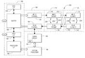
- FIG. 3is a functional block diagram of the data storage device of FIG. 1 .
- FIG. 4is a functional block diagram of the data reading and writing assembly of FIG. 3 with a write-safe detection circuit connected to the analog buffer head voltage terminal of the preamplifier.
- FIG. 5graphically illustrates a write current and a corresponding write-safe signal of an operative write element
- FIG. 6similarly graphically illustrates an inoperative write element.
- FIG. 7is a WRITE ELEMENT ENABLE VERIFICATION routine, illustrative of a method in accordance with embodiments of the present invention for on-the-fly verifying an enabled mode of the write element during the data writing mode.
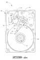
- FIG. 1shown therein is a plan view of a disc drive 100 constructed in accordance with preferred embodiments of the present invention.
- the disc drive 100includes a head-disc assembly (HDA) 101 and a disc drive printed wiring assembly (PWA) which is mounted to the underside of the HDA 101 and thus, not visible in FIG. 1 .
- the PWAprovides circuitry necessary to control the operation of the HDA 101 and to transfer data between the HDA 101 and a host computer in which the disc drive 100 can be mounted in a user environment.
- the HDA 101includes a base deck 102 to which various disc drive components are mounted.
- a top coverwhich has been omitted from FIG. 1 to facilitate the present discussion, cooperates with the base deck 102 to form an internal, sealed environment for the disc drive 100 .
- a spindle motor 104is provided to rotate a stack of discs 106 at a constant high speed, with a disc clamp 108 securing the discs to the spindle motor 104 .
- a controllably positionable actuator assembly 110which rotates about a cartridge bearing assembly 112 in response to currents applied to a coil (a portion of which is shown at 113 ) of a voice coil motor (VCM) 114 .
- the actuator assembly 110includes a plurality of arms from which corresponding flexure assemblies extend, the topmost of which are identified at 116 and 118 , respectively.
- Heads 120are provided at distal ends of the flexure assemblies 116 , 118 and are supported over the discs 106 by air bearings established by air currents set up by the rotation of the discs 106 .
- a latch assembly 121is provided to secure the heads 120 over landing zones, such as at the innermost diameters of the discs 106 when the disc drive 100 is deactivated.
- a flex circuit assembly 122provides electrical communication paths between the actuator assembly 110 and the disc drive PWA.
- each of the heads 120includes a thin-film inductive write element 132 and a magnetoresistive (MR) read element 134 .
- the write element 132writes data to the corresponding disc 106 by generating a time varying electromagnetic field (indicated generally at 136 ) across a gap 138 in response to write currents applied to the write element 132 .
- the electromagnetic field 136operates to selectively magnetize the disc 106 along a direction of movement of the disc 106 (as indicated by arrow 140 ). Magnetic flux transitions result at locations where reversals in the magnetization of the disc occur, such as shown at 142 .
- the read element 134preferably disposed in the write gap 138 of the write element 132 , is characterized as providing a changed electrical resistance in the presence of an electromagnetic field of selected orientation. Hence, by passing a bias current through the read element 134 , previously stored data can be transduced from the magnetized disc surface and converted to a readback signal in relation to changes in the voltage across the read element.
- FIG. 3illustrates a generalized functional block diagram of the control electronics arranged on the disc drive PWA in accordance with preferred embodiments of the present invention.
- One of the heads 120is illustrated, with corresponding write and read elements 132 , 134 .
- a preamplifier circuit 174includes a write driver 176 and a read amplifier 178 .
- the write driver 176applies write currents to the write element 132 and the read amplifier 178 applies a read bias current to the read element 134 .
- a communication channel 180is operably connected to the preamplifier 174 , and includes a write channel 182 which encodes and serializes input user data for writing by the write driver 176 , and a read channel 184 which receives readback signals from the read amplifier 178 and reconstructs previously stored user data therefrom.
- Servo data from the disc 106is passed from the read channel 184 to a servo circuit 186 , which includes a programmable digital signal processor (DSP) 187 to carry out head 120 positioning operations.
- An interface circuit 188has a buffer 190 to temporarily store data during data transfer operations between the discs 106 and a host computer. Transfers between the buffer 190 and discs 106 are controlled by a disc interface 192 , and transfers between the buffer 190 and the host computer are controlled by a host interface 194 .
- a processor interface 196enables communication between the interface circuit 188 and a system processor 198 , which controls overall operation of the disc drive 100 .
- the disc drive 100can be said to comprise a data reading and writing assembly 200 comprising three constituent parts—the head 120 , the preamplifier 174 , and an electrical interconnect 202 electrically connecting the head 120 and the preamplifier 174 .
- the read/write head 120comprises the write element 132 and the read element 134 , both adjacent the recording surface of the data storage disc 106 .
- the preamplifier 174comprises the write driver 176 applying a series of write currents for writing data to the recording surface and the read amplifier 178 for reading stored data from the recording surface.
- the interconnect 202joins the write driver 176 to the write element 132 so as to generate time-varying electromagnetic fields selectively magnetizing the recording surface in response to the write currents.
- the interconnect 202also joins the read amplifier 178 to the read element 134 so as to transduce magnetization vectors on the recording surface associated with stored data.
- the read amplifier 178is activated to generate the bias current during the time that the write driver 176 is activated to send a write current to the write element 132 , then the reversal in the writing current 142 (FIG. 2) generates an electromagnetic coupling effect in the bias current.
- the electromagnetic couplingoccurs in all three constituent parts of the data reading and writing assembly 200 at various magnitudes based on the characteristic construction of the parts. That is, if the head 120 has a properly wound and connected transducer coil, then an expected electromagnetic coupling effect 204 will occur between the write element 132 and the read element 134 .
- Summing the constituent coupling effects 204 , 206 , 208can provide a write-safe signal indicative of a data reading and writing assembly 200 that is operative. That is, by comparing the write-safe signal to a predetermined threshold value then defective and marginal components can be screened. For example, if the write element 132 is either electrically shorted or electrically open then no constituent coupling effect 204 will be produced, thereby decreasing the value of the write-safe signal.
- FIG. 4diagrammatically illustrates the data reading and writing assembly 200 illustrating one manner of detecting the write-safe signal.
- a detection circuit 210is connected to the analog buffer head voltage (ABHV) terminal 212 of the preamplifier 174 .
- the detection circuit 210can provide on-board continuous monitoring of the write-safe signal, and communicate with the system processor 198 to compare the value of the write-safe signal to a saved threshold value in order to control the operations of the disc drive 100 accordingly.
- the minimum expected write-safe signal levelis determined and a threshold value is preselected and saved such that an observed write-safe value less than the threshold value indicates an inoperative data reading and writing assembly 200 .
- the coupling effectinduces voltage transitions in the bias current that are detectable by the detection circuit 210 .
- FIG. 5graphically illustrates this screening process by the detection circuit 210 .
- a write signalsuch as a 2T signal, curve 220 and the write-safe signal 222 are each plotted against a common x-axis representing elapsed time and a common y-axis representing respective signal amplitudes.
- the write current signal 220generally represents pulsed write currents that are applied by the write over 176 (FIG. 3) to the write element 132 (FIG. 3) to selectively magnetize the disc 106 (FIG. 1 ). Transitions in the write current polarity 224 generate corresponding flux transitions 142 (FIG. 2) on the disc surface.
- the coupling electromagnetic signal, or write-safe signal, 222generally represents the sum of the constituent coupling effects of the preamplifier 174 , the head 120 , and the interconnect 202 .
- the write-safe signal 222has positive and negative peaks 226 associated with the magnitude of the coupling effects.
- a predetermined threshold value 228is saved and compared to the amplitude of the peaks, such as with a peak detect method, to determine a write-safe signal 222 indicative of a properly operating data reading and writing assembly 200 . If, for example, the write element 132 (FIG. 3) is inoperative, such as because of an electrical short-circuit or an electrical open-circuit, then the amplitude 226 will be correspondingly reduced.
- FIG. 6illustrates this case where the amplitude 230 is less than the threshold value 228.
- the threshold value 228(FIG. 5) is selected so as to indicate an inoperative or marginal condition of the write element 132 . Accordingly, it is necessary to determine the value of the constituent coupling effect contributed only by the write element 132 to the write-safe signal.
- the contribution made by the preamplifier 174can be determined by short-circuiting the output terminals 238 , 240 (FIG. 4) and disconnecting the interconnect 202 from the preamplifier 174 . In an experimental trial it was determined that the preamplifier 174 accounted for 34% of the total write-safe signal, such that the interconnect 202 and the head 120 accounted for the balance of 66% of the total write-safe signal.
- the output terminals 238 , 240 from the preamplifier 174can be unshorted and the interconnect 202 reconnected. Then the write element 132 is electrically disconnected from the interconnect 202 .
- the threshold value (V T )can be set nominally at 55% of the total observed write-safe signal value to screen for inoperative heads 120 .
- the embodiments of the present inventioncontemplate a method for writing data in a data storage device by the apparatus described hereinabove.
- the methodcomprises: generating the write current signal 224 associated with the data to be written with the write driver 176 portion of the preamplifier 174 ; transmitting the write current signal 224 along the interconnect 202 to the magnetoresistive write element 132 portion of the head 120 to generate the time-varying electromagnetic field 136 imparting flux transitions 142 associated with the data in the data storage portion of the data storage device; supplying the bias current to the read element 134 portion of the head 120 ; while transmitting the write current, simultaneously reading the electromagnetic coupling signal 222 comprising constituent coupling signals of the preamplifier 206 , the interconnect 208 and the head 204 ; and comparing the electromagnetic coupling signal 222 to the threshold value 228 indicative of the write-safe condition of the write element 132 .
- the embodimentscontemplate a method wherein the reading step is accomplished by connecting a detection circuit 210 to the analog buffer head voltage terminal 212 of the preamplifier 174 .
- a minimum or threshold expected electromagnetic coupling signalcan be determined such that a write-safe condition is indicated when the observed write-safe signal is greater than the threshold value.
- the constituent coupling signal of the preamplifier 206can be determined by short-circuiting the output terminals 238 , 240 of the preamplifier 174 and disconnecting the interconnect 202 while generating the write current signal 224 .
- the constituent coupling signal of the interconnect 208can be determined by subsequently unshorting the output terminals 238 , 240 , reconnecting the interconnect 202 , and removing the write element 132 of the head 120 .
- the write element 132can be removed by either short-circuiting the input terminals of the head 120 or by disconnecting the input lead of the write element 132 .
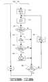
- FIG. 7provides a flow chart for a WRITE VERIFICATION routine 250 , illustrative of steps carried out by the disc drive 100 in accordance with a preferred embodiment to perform closed-loop write verification of data written to the discs 106 .
- the first set of data to be writtenis selected, as shown by step 252 . While the amount of data in the first set of data can vary depending on the application, preferably the first set of data represents an amount that can be accommodated by the user data field of a selected data block, such as 512 kilobytes (kB). Of course, a large user file is typically broken down and written to a number of data blocks, with the file being transferred to the buffer 190 and incrementally outputted to the write channel 182 .
- kB512 kilobytes
- the write channel 182operates to encode and serialize the data to enable the write driver 176 in block 254 .
- This operationincludes run-length limited (RLL) and error correction code (ECC) encoding, to facilitate subsequent retrieval of the recorded data.
- RLLrun-length limited
- ECCerror correction code
- the write currents generated at block 254are applied to the write element 132 in block 256 to generate the time-varying electromagnetic field necessary to write the data to the corresponding data field on the disc 106 .
- the detection circuit 210detects the time-varying electromagnetic field, or write-safe signal, which is the sum of the electromagnetic coupling effects of the preamplifier 174 , the head 120 , and the interconnect 202 .
- the write-safe signalis generated in response to the electromagnetic fields from the write driver 174 , the write element 132 , and the interconnect 202 , and not from the selective magnetization of the disc 106 .
- the detection circuit 210senses the operation of the constituent parts in real time, or on-the-fly, unlike conventional write verification schemes where the read element 134 subsequently transduces previously written data from the disc 106 .
- the value of the write-safe signalis compared to a stored threshold value. If the write-safe signal is less than the threshold value then the data block is marked for subsequent evaluation in block 262 . Such marking is typically achieved using a status register which indicates the status of the various data blocks of the disc drive 100 .
- the routinenext determines whether additional sets of data remain to be written at block 264 ; if so, the next block of data is selected in block 266 and control returns to block 254 .
- routine 268determines whether any of the accessed data blocks have been marked for further evaluation. If so, the first such marked data block is selected at block 270 and a conventional read verification operation is performed at block 272 . That is, the read element 134 is positioned over the associated data block to transduce the selective magnetization of the data block to generate a readback signal that is presented to the read channel 184 for reconstruction. If any uncorrected errors are detected in the recovered data by block 274 , the error recovery routines are applied at block 276 in an attempt to recover the data. Such routines can involve adjustment of various read channel and preamplifier parameters, application of a position offset to move the read element away a selected distance form the center of the track, etc.
- the embodiments of the present inventioncontemplate a disc drive (such as 100 ) comprising a rotatable disc (such as 106 ) having a magnetic recording surface, and a data reading and writing assembly (such as 200 ).
- the data reading and writing assemblycomprises a head (such as 120 ) comprising a write element (such as 132 ) and a read element (such as 134 ), both adjacent the recording surface; a preamplifier (such as 174 ) comprising a write driver (such as 176 ) applying a series of write currents (such as 224 ) for writing data to the recording surface and a read amplifier (such as 178 ) for reading stored data from the recording surface; and an interconnect (such as 202 ) joining the write driver to the write element so as to generate time-varying magnetic fields (such as 136 ) selectively magnetizing the recording surface in response to the write currents, and joining the read amplifier to the read element so as to transduce magnetization vectors on the recording surface associated with stored data.
- the disc drivefurthermore comprises a detection circuit (such as 210 ) connected to the data reading and writing assembly, receiving a write-safe signal (such as 222 ) indicative of a write-safe condition, the write-safe signal comprising a sum of constituent operable magnetic coupling values of the read/write head (such as 204 ), the preamplifier (such as 206 ) and the interconnect (such as 208 ).
- a detection circuitsuch as 210
- receives a write-safe signal(such as 222 ) indicative of a write-safe condition
- the write-safe signalcomprising a sum of constituent operable magnetic coupling values of the read/write head (such as 204 ), the preamplifier (such as 206 ) and the interconnect (such as 208 ).
- the detection circuitis connected to the preamplifier and receives the write-safe signal when a bias current is directed to the read element while writing data to the recording surface, such that a reversal in the writing current (such as 142 ) generates an electromagnetic coupling effect in the bias current.
- An advantageous constructioncomprises adaptively connecting the circuit to the analog buffer head voltage terminal (such as 212 ) of the preamplifier.
- Embodiments of the present inventionfurther contemplate a method for writing data in a data storage device, comprising: (a) generating a write current signal associated with the data to be written with a write driver portion of a preamplifier; (b) transmitting the write current signal along an interconnect to a magnetoresistive write element portion of a read/write head to generate a time-varying electromagnetic field imparting flux transitions associated with the data in a data storage portion of the data storage device (such as 254 ); (c) supplying a bias current to a read portion of the head; (d) while transmitting the write current, simultaneously reading an electromagnetic coupling signal comprising constituent coupling signals of the preamplifier, the interconnect and the read/write head (such as 258 ); and (e) comparing the electromagnetic coupling signal to a threshold value indicative of a write-safe condition of the write element (such as 260 ).
Landscapes
- Engineering & Computer Science (AREA)
- Signal Processing (AREA)
- Digital Magnetic Recording (AREA)
Abstract
Description
Claims (20)
Priority Applications (2)
| Application Number | Priority Date | Filing Date | Title |
|---|---|---|---|
| US10/056,496US6765736B2 (en) | 2001-06-29 | 2002-01-24 | Write-safe condition verification apparatus and method for the write element in a disc drive |
| PCT/US2003/001715WO2003063139A2 (en) | 2002-01-24 | 2003-01-21 | Write-safe condition verification apparatus and method for the write element in a disc drive |
Applications Claiming Priority (2)
| Application Number | Priority Date | Filing Date | Title |
|---|---|---|---|
| US30219501P | 2001-06-29 | 2001-06-29 | |
| US10/056,496US6765736B2 (en) | 2001-06-29 | 2002-01-24 | Write-safe condition verification apparatus and method for the write element in a disc drive |
Publications (2)
| Publication Number | Publication Date |
|---|---|
| US20030002187A1 US20030002187A1 (en) | 2003-01-02 |
| US6765736B2true US6765736B2 (en) | 2004-07-20 |
Family
ID=27609291
Family Applications (1)
| Application Number | Title | Priority Date | Filing Date |
|---|---|---|---|
| US10/056,496Expired - Fee RelatedUS6765736B2 (en) | 2001-06-29 | 2002-01-24 | Write-safe condition verification apparatus and method for the write element in a disc drive |
Country Status (2)
| Country | Link |
|---|---|
| US (1) | US6765736B2 (en) |
| WO (1) | WO2003063139A2 (en) |
Cited By (5)
| Publication number | Priority date | Publication date | Assignee | Title |
|---|---|---|---|---|
| US7477467B1 (en)* | 2003-11-25 | 2009-01-13 | Marvell International Ltd. | Preamp circuit including a loopback mode for data storage |
| US7853747B2 (en) | 2003-03-10 | 2010-12-14 | Marvell International Ltd. | Method and system for using an external bus controller in embedded disk controllers |
| US7870346B2 (en) | 2003-03-10 | 2011-01-11 | Marvell International Ltd. | Servo controller interface module for embedded disk controllers |
| US7975110B1 (en) | 2003-03-10 | 2011-07-05 | Marvell International Ltd. | Method and system for supporting multiple external serial port devices using a serial port controller in embedded disk controllers |
| US8189285B1 (en) | 2003-03-10 | 2012-05-29 | Marvell International Ltd. | Method and system for automatic time base adjustment for disk drive servo controllers |
Families Citing this family (6)
| Publication number | Priority date | Publication date | Assignee | Title |
|---|---|---|---|---|
| US6765736B2 (en)* | 2001-06-29 | 2004-07-20 | Seagate Technology Llc | Write-safe condition verification apparatus and method for the write element in a disc drive |
| US7130138B2 (en)* | 2003-12-15 | 2006-10-31 | Seagate Technology Llc | Environmental stress protection scheme for a data storage device |
| US7619843B2 (en)* | 2006-11-14 | 2009-11-17 | Hitachi Global Storage Technologies Netherlands, B.V. | Write through drivers for disk drive systems |
| US10734016B2 (en) | 2018-08-21 | 2020-08-04 | Marvell Asia Pte, Ltd. | Pulse-based writing for magnetic storage media |
| US12197738B2 (en) | 2019-01-31 | 2025-01-14 | Marvell Asia Pte, Ltd. | Health management for magnetic storage media |
| US11450348B2 (en) | 2019-01-31 | 2022-09-20 | Marvell Asia Pte, Ltd. | Health management for magnetic storage media |
Citations (7)
| Publication number | Priority date | Publication date | Assignee | Title |
|---|---|---|---|---|
| US5495378A (en) | 1995-01-30 | 1996-02-27 | Seagate Technology, Inc. | Magnetoresistive sensor with improved performance and processability |
| US5737152A (en) | 1995-10-27 | 1998-04-07 | Quantum Corporation | Suspension with multi-layered integrated conductor trace array for optimized electrical parameters |
| US5754369A (en) | 1996-10-03 | 1998-05-19 | Quantum Corporation | Head suspension with self-shielding integrated conductor trace array |
| US5812344A (en) | 1997-05-12 | 1998-09-22 | Quantum Corporation | Suspension with integrated conductor trace array having optimized cross-sectional high frequency current density |
| US5909342A (en) | 1996-02-20 | 1999-06-01 | Seagate Technology, Inc. | Planar flexible circuit package for coupling transducers with carriage mounted circuitry |
| US6014281A (en) | 1997-12-04 | 2000-01-11 | International Business Machines Corporation | Using a read element and a read/write coupling path to detect write-safe conditions |
| US6266202B1 (en) | 1998-06-05 | 2001-07-24 | Seagate Technology Llc | Closed loop write verification in a disc drive |
Family Cites Families (8)
| Publication number | Priority date | Publication date | Assignee | Title |
|---|---|---|---|---|
| US5430584A (en)* | 1991-10-18 | 1995-07-04 | International Microelectronic Products | Disk drive interface combining a magneto-resistive read and inductive write circuits |
| US5357379A (en)* | 1993-07-02 | 1994-10-18 | Exar Corporation | Read/write circuit with switchable head resistance for read and write modes |
| US5589777A (en)* | 1995-06-21 | 1996-12-31 | Hewlett-Packard Company | Circuit and method for testing a disk drive head assembly without probing |
| DE69516914T2 (en)* | 1995-09-06 | 2000-10-05 | Seagate Technology, Inc. | DYNAMICALLY PROGRAMMABLE WRITE CURRENT AND READ PRE-CURRENT FOR A MAGNETORESISTIVE HEAD |
| US5729208A (en)* | 1995-10-03 | 1998-03-17 | Texas Instruments Incorporated | Apparatus for detecting open circuit in hard disk drive |
| US5726821A (en)* | 1995-12-22 | 1998-03-10 | Western Digital Corporation | Programmable preamplifier unit with serial interface for disk data storage device using MR heads |
| US6130795A (en)* | 1998-05-05 | 2000-10-10 | International Business Machines Corporation | Method and apparatus to sense and report connection integrity of a differential ECL transmission line having proper parallel termination |
| US6765736B2 (en)* | 2001-06-29 | 2004-07-20 | Seagate Technology Llc | Write-safe condition verification apparatus and method for the write element in a disc drive |
- 2002
- 2002-01-24USUS10/056,496patent/US6765736B2/ennot_activeExpired - Fee Related
- 2003
- 2003-01-21WOPCT/US2003/001715patent/WO2003063139A2/ennot_activeApplication Discontinuation
Patent Citations (7)
| Publication number | Priority date | Publication date | Assignee | Title |
|---|---|---|---|---|
| US5495378A (en) | 1995-01-30 | 1996-02-27 | Seagate Technology, Inc. | Magnetoresistive sensor with improved performance and processability |
| US5737152A (en) | 1995-10-27 | 1998-04-07 | Quantum Corporation | Suspension with multi-layered integrated conductor trace array for optimized electrical parameters |
| US5909342A (en) | 1996-02-20 | 1999-06-01 | Seagate Technology, Inc. | Planar flexible circuit package for coupling transducers with carriage mounted circuitry |
| US5754369A (en) | 1996-10-03 | 1998-05-19 | Quantum Corporation | Head suspension with self-shielding integrated conductor trace array |
| US5812344A (en) | 1997-05-12 | 1998-09-22 | Quantum Corporation | Suspension with integrated conductor trace array having optimized cross-sectional high frequency current density |
| US6014281A (en) | 1997-12-04 | 2000-01-11 | International Business Machines Corporation | Using a read element and a read/write coupling path to detect write-safe conditions |
| US6266202B1 (en) | 1998-06-05 | 2001-07-24 | Seagate Technology Llc | Closed loop write verification in a disc drive |
Cited By (12)
| Publication number | Priority date | Publication date | Assignee | Title |
|---|---|---|---|---|
| US7853747B2 (en) | 2003-03-10 | 2010-12-14 | Marvell International Ltd. | Method and system for using an external bus controller in embedded disk controllers |
| US7870346B2 (en) | 2003-03-10 | 2011-01-11 | Marvell International Ltd. | Servo controller interface module for embedded disk controllers |
| US7870320B1 (en) | 2003-03-10 | 2011-01-11 | Marvell International Ltd. | Interrupt controller for prioritizing interrupt requests in an embedded disk controller |
| US7975110B1 (en) | 2003-03-10 | 2011-07-05 | Marvell International Ltd. | Method and system for supporting multiple external serial port devices using a serial port controller in embedded disk controllers |
| US8189285B1 (en) | 2003-03-10 | 2012-05-29 | Marvell International Ltd. | Method and system for automatic time base adjustment for disk drive servo controllers |
| US7477467B1 (en)* | 2003-11-25 | 2009-01-13 | Marvell International Ltd. | Preamp circuit including a loopback mode for data storage |
| US7852585B1 (en) | 2003-11-25 | 2010-12-14 | Marvell International Ltd. | Preamp circuit including a loopback mode for data storage devices |
| US8077415B1 (en) | 2003-11-25 | 2011-12-13 | Marvell International Ltd. | Preamp circuit including a loopback mode for data storage devices |
| US8379341B1 (en) | 2003-11-25 | 2013-02-19 | Marvell International Ltd. | Preamp circuit including a loopback mode for data storage devices |
| US8514508B1 (en) | 2003-11-25 | 2013-08-20 | Marvell International Ltd. | Preamp circuit including a loopback mode for data storage devices |
| US8654469B1 (en) | 2003-11-25 | 2014-02-18 | Marvell International Ltd. | Preamp circuit including a loopback mode for data storage devices |
| US8947808B1 (en) | 2003-11-25 | 2015-02-03 | Marvell International Ltd. | Preamp circuit including a loopback mode for data storage devices |
Also Published As
| Publication number | Publication date |
|---|---|
| WO2003063139A3 (en) | 2004-02-19 |
| US20030002187A1 (en) | 2003-01-02 |
| WO2003063139A2 (en) | 2003-07-31 |
Similar Documents
| Publication | Publication Date | Title |
|---|---|---|
| US6249890B1 (en) | Detecting head readback response degradation in a disc drive | |
| US5233482A (en) | Thermal asperity compensation for PRML data detection | |
| EP0853310B1 (en) | Magnetic storage apparatus using a magnetoresistive element | |
| US7656600B2 (en) | Monitoring transducer potential to detect an operating condition | |
| US6356404B1 (en) | Simultaneously biasing multiple magneto-resistive read elements | |
| US6765736B2 (en) | Write-safe condition verification apparatus and method for the write element in a disc drive | |
| EP0746850A1 (en) | System and method for encoding a servo address | |
| US7088537B2 (en) | Removing residual magnetization in a data transducer | |
| US20020181131A1 (en) | User data wedge media certification in a disc drive data handling system | |
| US7206990B2 (en) | Data sector error handling mechanism | |
| US6696832B2 (en) | Method and apparatus for testing transducer heads in magnetic storage systems | |
| JP4054640B2 (en) | Method and apparatus for recovering head instability in data storage system | |
| US6320714B1 (en) | Reduced head population detection in a disc drive | |
| US6266202B1 (en) | Closed loop write verification in a disc drive | |
| US6373649B1 (en) | Reduced head population detection in a disc drive | |
| US6822814B2 (en) | Write head collision detection using MR read element in disc drives | |
| US6115201A (en) | Disc drive head bias current optimization | |
| US6104558A (en) | System and method of encoding an index mark into a servo address | |
| US5969896A (en) | Magnetic recording/reproducing device with a function of correcting waveform of magnetoresistive-effect head | |
| US6421193B1 (en) | Method and apparatus for detecting, logging and recovering from errors caused by multiple thermal asperities in a sector | |
| US6532126B1 (en) | Head switching sequence in a disc drive employing head bias currents | |
| US8045281B2 (en) | Method of setting write factor in hard disk drive and hard disk drive using the same | |
| US6785083B2 (en) | Application of reduced bias levels to disc drive read elements during periods of inactivity | |
| KR100562146B1 (en) | M. R-bias current optimization method | |
| JP3924405B2 (en) | Data block writing method, apparatus, and storage medium |
Legal Events
| Date | Code | Title | Description |
|---|---|---|---|
| AS | Assignment | Owner name:JPMORGAN CHASE BANK, AS COLLATERAL AGENT, NEW YORK Free format text:SECURITY AGREEMENT;ASSIGNOR:SEAGATE TECHNOLOGY LLC;REEL/FRAME:013177/0001 Effective date:20020513 Owner name:JPMORGAN CHASE BANK, AS COLLATERAL AGENT,NEW YORK Free format text:SECURITY AGREEMENT;ASSIGNOR:SEAGATE TECHNOLOGY LLC;REEL/FRAME:013177/0001 Effective date:20020513 | |
| FEPP | Fee payment procedure | Free format text:PAYOR NUMBER ASSIGNED (ORIGINAL EVENT CODE: ASPN); ENTITY STATUS OF PATENT OWNER: LARGE ENTITY | |
| AS | Assignment | Owner name:SEAGATE TECHNOLOGY LLC, CALIFORNIA Free format text:RELEASE OF SECURITY INTERESTS IN PATENT RIGHTS;ASSIGNOR:JPMORGAN CHASE BANK, N.A. (FORMERLY KNOWN AS THE CHASE MANHATTAN BANK AND JPMORGAN CHASE BANK), AS ADMINISTRATIVE AGENT;REEL/FRAME:016958/0607 Effective date:20051130 | |
| FPAY | Fee payment | Year of fee payment:4 | |
| REMI | Maintenance fee reminder mailed | ||
| AS | Assignment | Owner name:WELLS FARGO BANK, NATIONAL ASSOCIATION, AS COLLATERAL AGENT AND SECOND PRIORITY REPRESENTATIVE, CALIFORNIA Free format text:SECURITY AGREEMENT;ASSIGNORS:MAXTOR CORPORATION;SEAGATE TECHNOLOGY LLC;SEAGATE TECHNOLOGY INTERNATIONAL;REEL/FRAME:022757/0017 Effective date:20090507 Owner name:JPMORGAN CHASE BANK, N.A., AS ADMINISTRATIVE AGENT AND FIRST PRIORITY REPRESENTATIVE, NEW YORK Free format text:SECURITY AGREEMENT;ASSIGNORS:MAXTOR CORPORATION;SEAGATE TECHNOLOGY LLC;SEAGATE TECHNOLOGY INTERNATIONAL;REEL/FRAME:022757/0017 Effective date:20090507 Owner name:JPMORGAN CHASE BANK, N.A., AS ADMINISTRATIVE AGENT Free format text:SECURITY AGREEMENT;ASSIGNORS:MAXTOR CORPORATION;SEAGATE TECHNOLOGY LLC;SEAGATE TECHNOLOGY INTERNATIONAL;REEL/FRAME:022757/0017 Effective date:20090507 Owner name:WELLS FARGO BANK, NATIONAL ASSOCIATION, AS COLLATE Free format text:SECURITY AGREEMENT;ASSIGNORS:MAXTOR CORPORATION;SEAGATE TECHNOLOGY LLC;SEAGATE TECHNOLOGY INTERNATIONAL;REEL/FRAME:022757/0017 Effective date:20090507 | |
| AS | Assignment | Owner name:SEAGATE TECHNOLOGY INTERNATIONAL, CALIFORNIA Free format text:RELEASE;ASSIGNOR:JPMORGAN CHASE BANK, N.A., AS ADMINISTRATIVE AGENT;REEL/FRAME:025662/0001 Effective date:20110114 Owner name:SEAGATE TECHNOLOGY HDD HOLDINGS, CALIFORNIA Free format text:RELEASE;ASSIGNOR:JPMORGAN CHASE BANK, N.A., AS ADMINISTRATIVE AGENT;REEL/FRAME:025662/0001 Effective date:20110114 Owner name:MAXTOR CORPORATION, CALIFORNIA Free format text:RELEASE;ASSIGNOR:JPMORGAN CHASE BANK, N.A., AS ADMINISTRATIVE AGENT;REEL/FRAME:025662/0001 Effective date:20110114 Owner name:SEAGATE TECHNOLOGY LLC, CALIFORNIA Free format text:RELEASE;ASSIGNOR:JPMORGAN CHASE BANK, N.A., AS ADMINISTRATIVE AGENT;REEL/FRAME:025662/0001 Effective date:20110114 | |
| AS | Assignment | Owner name:THE BANK OF NOVA SCOTIA, AS ADMINISTRATIVE AGENT, CANADA Free format text:SECURITY AGREEMENT;ASSIGNOR:SEAGATE TECHNOLOGY LLC;REEL/FRAME:026010/0350 Effective date:20110118 Owner name:THE BANK OF NOVA SCOTIA, AS ADMINISTRATIVE AGENT, Free format text:SECURITY AGREEMENT;ASSIGNOR:SEAGATE TECHNOLOGY LLC;REEL/FRAME:026010/0350 Effective date:20110118 | |
| FPAY | Fee payment | Year of fee payment:8 | |
| AS | Assignment | Owner name:SEAGATE TECHNOLOGY US HOLDINGS, INC., CALIFORNIA Free format text:TERMINATION AND RELEASE OF SECURITY INTEREST IN PATENT RIGHTS;ASSIGNOR:WELLS FARGO BANK, NATIONAL ASSOCIATION, AS COLLATERAL AGENT AND SECOND PRIORITY REPRESENTATIVE;REEL/FRAME:030833/0001 Effective date:20130312 Owner name:SEAGATE TECHNOLOGY INTERNATIONAL, CAYMAN ISLANDS Free format text:TERMINATION AND RELEASE OF SECURITY INTEREST IN PATENT RIGHTS;ASSIGNOR:WELLS FARGO BANK, NATIONAL ASSOCIATION, AS COLLATERAL AGENT AND SECOND PRIORITY REPRESENTATIVE;REEL/FRAME:030833/0001 Effective date:20130312 Owner name:EVAULT INC. (F/K/A I365 INC.), CALIFORNIA Free format text:TERMINATION AND RELEASE OF SECURITY INTEREST IN PATENT RIGHTS;ASSIGNOR:WELLS FARGO BANK, NATIONAL ASSOCIATION, AS COLLATERAL AGENT AND SECOND PRIORITY REPRESENTATIVE;REEL/FRAME:030833/0001 Effective date:20130312 Owner name:SEAGATE TECHNOLOGY LLC, CALIFORNIA Free format text:TERMINATION AND RELEASE OF SECURITY INTEREST IN PATENT RIGHTS;ASSIGNOR:WELLS FARGO BANK, NATIONAL ASSOCIATION, AS COLLATERAL AGENT AND SECOND PRIORITY REPRESENTATIVE;REEL/FRAME:030833/0001 Effective date:20130312 | |
| REMI | Maintenance fee reminder mailed | ||
| LAPS | Lapse for failure to pay maintenance fees | ||
| STCH | Information on status: patent discontinuation | Free format text:PATENT EXPIRED DUE TO NONPAYMENT OF MAINTENANCE FEES UNDER 37 CFR 1.362 | |
| FP | Lapsed due to failure to pay maintenance fee | Effective date:20160720 | |
| AS | Assignment | Owner name:SEAGATE TECHNOLOGY PUBLIC LIMITED COMPANY, CALIFORNIA Free format text:RELEASE BY SECURED PARTY;ASSIGNOR:THE BANK OF NOVA SCOTIA;REEL/FRAME:072193/0001 Effective date:20250303 Owner name:SEAGATE TECHNOLOGY, CALIFORNIA Free format text:RELEASE BY SECURED PARTY;ASSIGNOR:THE BANK OF NOVA SCOTIA;REEL/FRAME:072193/0001 Effective date:20250303 Owner name:SEAGATE TECHNOLOGY HDD HOLDINGS, CALIFORNIA Free format text:RELEASE BY SECURED PARTY;ASSIGNOR:THE BANK OF NOVA SCOTIA;REEL/FRAME:072193/0001 Effective date:20250303 Owner name:I365 INC., CALIFORNIA Free format text:RELEASE BY SECURED PARTY;ASSIGNOR:THE BANK OF NOVA SCOTIA;REEL/FRAME:072193/0001 Effective date:20250303 Owner name:SEAGATE TECHNOLOGY LLC, CALIFORNIA Free format text:RELEASE BY SECURED PARTY;ASSIGNOR:THE BANK OF NOVA SCOTIA;REEL/FRAME:072193/0001 Effective date:20250303 Owner name:SEAGATE TECHNOLOGY INTERNATIONAL, CAYMAN ISLANDS Free format text:RELEASE BY SECURED PARTY;ASSIGNOR:THE BANK OF NOVA SCOTIA;REEL/FRAME:072193/0001 Effective date:20250303 Owner name:SEAGATE HDD CAYMAN, CAYMAN ISLANDS Free format text:RELEASE BY SECURED PARTY;ASSIGNOR:THE BANK OF NOVA SCOTIA;REEL/FRAME:072193/0001 Effective date:20250303 Owner name:SEAGATE TECHNOLOGY (US) HOLDINGS, INC., CALIFORNIA Free format text:RELEASE BY SECURED PARTY;ASSIGNOR:THE BANK OF NOVA SCOTIA;REEL/FRAME:072193/0001 Effective date:20250303 |