US6765259B2 - Non-volatile memory transistor array implementing “H” shaped source/drain regions and method for fabricating same - Google Patents
Non-volatile memory transistor array implementing “H” shaped source/drain regions and method for fabricating sameDownload PDFInfo
- Publication number
- US6765259B2 US6765259B2US10/233,310US23331002AUS6765259B2US 6765259 B2US6765259 B2US 6765259B2US 23331002 AUS23331002 AUS 23331002AUS 6765259 B2US6765259 B2US 6765259B2
- Authority
- US
- United States
- Prior art keywords
- forming
- dielectric layer
- layer
- source
- regions
- Prior art date
- Legal status (The legal status is an assumption and is not a legal conclusion. Google has not performed a legal analysis and makes no representation as to the accuracy of the status listed.)
- Expired - Fee Related, expires
Links
- 238000000034methodMethods0.000titleclaimsdescription37
- 238000002955isolationMethods0.000claimsabstractdescription29
- 239000000758substrateSubstances0.000claimsabstractdescription23
- 239000004065semiconductorSubstances0.000claimsabstractdescription13
- 229910021420polycrystalline siliconInorganic materials0.000claimsdescription24
- 229920005591polysiliconPolymers0.000claimsdescription23
- 229910052581Si3N4Inorganic materials0.000claimsdescription20
- 239000007943implantSubstances0.000claimsdescription20
- HQVNEWCFYHHQES-UHFFFAOYSA-Nsilicon nitrideChemical compoundN12[Si]34N5[Si]62N3[Si]51N64HQVNEWCFYHHQES-UHFFFAOYSA-N0.000claimsdescription20
- VYPSYNLAJGMNEJ-UHFFFAOYSA-NSilicium dioxideChemical compoundO=[Si]=OVYPSYNLAJGMNEJ-UHFFFAOYSA-N0.000claimsdescription18
- 229910052814silicon oxideInorganic materials0.000claimsdescription18
- 229910021332silicideInorganic materials0.000claimsdescription14
- FVBUAEGBCNSCDD-UHFFFAOYSA-Nsilicide(4-)Chemical compound[Si-4]FVBUAEGBCNSCDD-UHFFFAOYSA-N0.000claimsdescription14
- 125000006850spacer groupChemical group0.000claimsdescription13
- 238000004519manufacturing processMethods0.000claimsdescription12
- 238000000151depositionMethods0.000claimsdescription11
- 239000012535impuritySubstances0.000claimsdescription11
- 239000003870refractory metalSubstances0.000claimsdescription10
- 230000001590oxidative effectEffects0.000claimsdescription8
- XUIMIQQOPSSXEZ-UHFFFAOYSA-NSiliconChemical compound[Si]XUIMIQQOPSSXEZ-UHFFFAOYSA-N0.000claimsdescription5
- 238000007254oxidation reactionMethods0.000claimsdescription5
- 229910052710siliconInorganic materials0.000claimsdescription5
- 239000010703siliconSubstances0.000claimsdescription5
- 230000003647oxidationEffects0.000claimsdescription4
- 239000011810insulating materialSubstances0.000claimsdescription2
- 238000000059patterningMethods0.000claimsdescription2
- 150000004767nitridesChemical class0.000abstractdescription2
- 238000003860storageMethods0.000abstractdescription2
- 229910052751metalInorganic materials0.000description15
- 239000002184metalSubstances0.000description15
- 238000009792diffusion processMethods0.000description10
- 238000010586diagramMethods0.000description8
- 229910052785arsenicInorganic materials0.000description7
- 229920002120photoresistant polymerPolymers0.000description7
- RQNWIZPPADIBDY-UHFFFAOYSA-Narsenic atomChemical compound[As]RQNWIZPPADIBDY-UHFFFAOYSA-N0.000description6
- IJGRMHOSHXDMSA-UHFFFAOYSA-NAtomic nitrogenChemical compoundN#NIJGRMHOSHXDMSA-UHFFFAOYSA-N0.000description4
- 239000002019doping agentSubstances0.000description4
- BHEPBYXIRTUNPN-UHFFFAOYSA-Nhydridophosphorus(.) (triplet)Chemical compound[PH]BHEPBYXIRTUNPN-UHFFFAOYSA-N0.000description4
- XHXFXVLFKHQFAL-UHFFFAOYSA-Nphosphoryl trichlorideChemical compoundClP(Cl)(Cl)=OXHXFXVLFKHQFAL-UHFFFAOYSA-N0.000description4
- ZOXJGFHDIHLPTG-UHFFFAOYSA-NBoronChemical compound[B]ZOXJGFHDIHLPTG-UHFFFAOYSA-N0.000description3
- 238000000137annealingMethods0.000description3
- 229910052796boronInorganic materials0.000description3
- 238000002513implantationMethods0.000description3
- 238000002347injectionMethods0.000description3
- 239000007924injectionSubstances0.000description3
- 150000002500ionsChemical class0.000description3
- 229910015900BF3Inorganic materials0.000description2
- RTAQQCXQSZGOHL-UHFFFAOYSA-NTitaniumChemical compound[Ti]RTAQQCXQSZGOHL-UHFFFAOYSA-N0.000description2
- -1arsenic ionsChemical class0.000description2
- 230000015572biosynthetic processEffects0.000description2
- WTEOIRVLGSZEPR-UHFFFAOYSA-Nboron trifluorideChemical compoundFB(F)FWTEOIRVLGSZEPR-UHFFFAOYSA-N0.000description2
- 239000010941cobaltSubstances0.000description2
- 229910017052cobaltInorganic materials0.000description2
- GUTLYIVDDKVIGB-UHFFFAOYSA-Ncobalt atomChemical compound[Co]GUTLYIVDDKVIGB-UHFFFAOYSA-N0.000description2
- 239000003989dielectric materialSubstances0.000description2
- 238000005516engineering processMethods0.000description2
- 239000002784hot electronSubstances0.000description2
- 238000012986modificationMethods0.000description2
- 230000004048modificationEffects0.000description2
- 229910052757nitrogenInorganic materials0.000description2
- 239000010936titaniumSubstances0.000description2
- 229910052719titaniumInorganic materials0.000description2
- 241000293849CordylanthusSpecies0.000description1
- UFHFLCQGNIYNRP-UHFFFAOYSA-NHydrogenChemical compound[H][H]UFHFLCQGNIYNRP-UHFFFAOYSA-N0.000description1
- OAICVXFJPJFONN-UHFFFAOYSA-NPhosphorusChemical compound[P]OAICVXFJPJFONN-UHFFFAOYSA-N0.000description1
- QVGXLLKOCUKJST-UHFFFAOYSA-Natomic oxygenChemical compound[O]QVGXLLKOCUKJST-UHFFFAOYSA-N0.000description1
- 230000000903blocking effectEffects0.000description1
- 238000005530etchingMethods0.000description1
- 239000001257hydrogenSubstances0.000description1
- 229910052739hydrogenInorganic materials0.000description1
- 230000014759maintenance of locationEffects0.000description1
- 239000001301oxygenSubstances0.000description1
- 229910052760oxygenInorganic materials0.000description1
- 229910052698phosphorusInorganic materials0.000description1
- 239000011574phosphorusSubstances0.000description1
- WQJQOUPTWCFRMM-UHFFFAOYSA-Ntungsten disilicideChemical compound[Si]#[W]#[Si]WQJQOUPTWCFRMM-UHFFFAOYSA-N0.000description1
- 229910021342tungsten silicideInorganic materials0.000description1
Images


Classifications
- H—ELECTRICITY
- H10—SEMICONDUCTOR DEVICES; ELECTRIC SOLID-STATE DEVICES NOT OTHERWISE PROVIDED FOR
- H10B—ELECTRONIC MEMORY DEVICES
- H10B43/00—EEPROM devices comprising charge-trapping gate insulators
- H10B43/30—EEPROM devices comprising charge-trapping gate insulators characterised by the memory core region
- H—ELECTRICITY
- H10—SEMICONDUCTOR DEVICES; ELECTRIC SOLID-STATE DEVICES NOT OTHERWISE PROVIDED FOR
- H10B—ELECTRONIC MEMORY DEVICES
- H10B69/00—Erasable-and-programmable ROM [EPROM] devices not provided for in groups H10B41/00 - H10B63/00, e.g. ultraviolet erasable-and-programmable ROM [UVEPROM] devices
- H—ELECTRICITY
- H10—SEMICONDUCTOR DEVICES; ELECTRIC SOLID-STATE DEVICES NOT OTHERWISE PROVIDED FOR
- H10D—INORGANIC ELECTRIC SEMICONDUCTOR DEVICES
- H10D30/00—Field-effect transistors [FET]
- H10D30/01—Manufacture or treatment
- H10D30/021—Manufacture or treatment of FETs having insulated gates [IGFET]
- H10D30/0413—Manufacture or treatment of FETs having insulated gates [IGFET] of FETs having charge-trapping gate insulators, e.g. MNOS transistors
- H—ELECTRICITY
- H10—SEMICONDUCTOR DEVICES; ELECTRIC SOLID-STATE DEVICES NOT OTHERWISE PROVIDED FOR
- H10D—INORGANIC ELECTRIC SEMICONDUCTOR DEVICES
- H10D30/00—Field-effect transistors [FET]
- H10D30/60—Insulated-gate field-effect transistors [IGFET]
- H10D30/69—IGFETs having charge trapping gate insulators, e.g. MNOS transistors
- H10D30/691—IGFETs having charge trapping gate insulators, e.g. MNOS transistors having more than two programming levels
- H—ELECTRICITY
- H10—SEMICONDUCTOR DEVICES; ELECTRIC SOLID-STATE DEVICES NOT OTHERWISE PROVIDED FOR
- H10D—INORGANIC ELECTRIC SEMICONDUCTOR DEVICES
- H10D62/00—Semiconductor bodies, or regions thereof, of devices having potential barriers
- H10D62/10—Shapes, relative sizes or dispositions of the regions of the semiconductor bodies; Shapes of the semiconductor bodies
- H10D62/124—Shapes, relative sizes or dispositions of the regions of semiconductor bodies or of junctions between the regions
- H10D62/126—Top-view geometrical layouts of the regions or the junctions
- G—PHYSICS
- G11—INFORMATION STORAGE
- G11C—STATIC STORES
- G11C16/00—Erasable programmable read-only memories
- G11C16/02—Erasable programmable read-only memories electrically programmable
- G11C16/04—Erasable programmable read-only memories electrically programmable using variable threshold transistors, e.g. FAMOS
- G11C16/0491—Virtual ground arrays
Definitions
- the present inventionrelates to non-volatile memory transistors. More specifically, the present invention relates to a method and structure of using a 2-bit non-volatile memory transistor to form a flash memory transistor array.
- a 2-bit non-volatile semiconductor memory transistorhas been described in U.S. Pat. No. 5,768,192, to Eitan. However, the manners of using 2-bit NVM transistors in a memory array have not yet been fully developed.
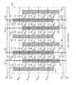
- FIG. 1is a schematic diagram illustrating a conventional memory block 100 .
- Memory block 100implements uses a plurality of 2-bit memory transistors, which are identified as memory transistors M X,Y , where X and Y represent the row and column locations, respectively, of the memory transistors within memory block 100 .
- memory block 100includes memory transistors M 0,0 -M 3,6 .
- the rowsextend along a first axis, and the columns extend along a second axis, perpendicular to the first axis.
- Each of the memory transistors M 0,0 -M 3,6includes two charge trapping regions, namely, a left charge trapping region and a right charge trapping region, thereby enabling each of memory transistors M 0,0 -M 3,6 to store 2-bits of data.
- the source and drain regions of memory transistors M 0,0 -M 3,6are formed by diffused regions 101 - 108 , which extend in parallel along the second axis. Diffused regions 101 - 108 also operate as bit lines within memory block 100 . Thus, diffused regions 101 - 108 are referred to as diffusion bit lines.
- ONO structures 111 - 117are located between adjacent diffusion bit lines 101 - 108 , as illustrated.
- the gates of the memory transistors in each roware commonly connected to a word line. More specifically, the memory transistors of rows 0 - 3 are connected to word lines WL 0 -WL 3 , respectively.
- the 2-bit memory transistors of memory block 100are accessed through high-voltage select transistors 131 - 138 and metal bit lines 141 - 144 .
- Metal bit lines 141 - 144are located in an interconnect layer that extends over the above-described elements of memory block 100 .
- High-voltage select transistors 131 - 138are designed to have gate oxide sufficient to withstand the high voltages required for programming and erasing the memory transistors. In general, select transistors 131 - 138 are controlled to selectively connect metal bit lines 141 - 144 to diffusion bit lines 101 - 108 .
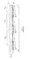
- FIG. 2is a cross sectional view of memory transistors M 0,0 and M 0,1 along the first axis through word line WL 0 .
- Diffusion bit lines 101 - 103are n-type regions formed in a p-type silicon semiconductor region 110 .
- Bit line oxide regions 124are formed over the diffusion bit lines 101 - 103 . Because the memory transistors in memory block 100 do not require field oxide for isolation, memory block 100 can be referred to as a fieldless array.
- ONO structures 111 and 112extend over bit line insulating regions 124 , diffusion bit lines 101 - 103 and substrate 110 in the manner illustrated.
- Word line WL 0is a polycide or salicide structure that includes a layer of conductively doped polycrystalline silicon 126 and an overlying layer of metal silicide 127 , and extends over ONO structures 111 and 112 (and bit line insulating regions 124 ).
- Word lines WL 0forms the control gate of memory transistors M 0,0 and M 0,1 .
- the fabrication of memory block 100is described in U.S. Pat. No. 6,346,442 by Aloni et al.
- Typical problems associated with memory block 100 and the corresponding memory transistorsinclude (1) relatively large source/drain series resistances due to the use of diffusion bit lines, (2) relatively deep source/drain junction depths due to the high thermal budget required by bit line oxidate regions, (3) an unadaptable structure with respect to advanced CMOS technology using self-aligned salicidation process (i.e., almost impossible to implement self-aligned salicide on word lines and source/drain regions), and (4) high bit line-to-bit line leakage, because the memory transistors are separated by active regions, without any general isolation structure.
- a flash memory array structurethat implements 2-bit non-volatile memory transistors and exhibits a relatively low source/drain series resistance, and a relatively low bit line resistance. It would further be desirable if the source/drain junction depth of the memory transistors in the array are relatively shallow (e.g., less than 0.1 microns). It would further be desirable if the flash memory array structure were capable of implementing a self-aligned salicidation process over both the gate and source/drain regions of the array. It would also be desirable if there were no leakage issues between bit lines of the flash memory array. It would further be desirable if the flash memory array exhibits low word line capacitance, thereby resulting in low RC delay and high-speed operation.
- the present inventionprovides an improved array structure for implementing a flash memory array using 2-bit non-volatile memory transistors.
- a flash memory arrayis defined as a non-volatile memory array that cannot be erased on a word-by-word basis, but which must be erased in blocks.
- the present inventionalso provides a method for fabricating this improved array structure, which is largely compatible with a conventional CMOS process flow.
- a non-volatile memory (NVM) arrayis fabricated with a plurality of 2-bit NVM transistors arranged in a plurality of rows extending along a first axis, and a plurality of columns extending along a second axis, perpendicular to the first axis.
- the non-volatile memory arrayincludes a plurality of field isolation regions located in a semiconductor substrate.
- the field isolation regionsare shallow trench isolation (STI) regions.
- a plurality of word linesextend over the semiconductor substrate along the first axis, wherein the word lines also form control gates of the 2-bit NVM transistors.
- Oxide-nitride-oxide (ONO) structuresare located between the substrate and the word lines, wherein the nitride layer of the ONO structures provides floating gate storage for the NVM transistors.
- a plurality of H-shaped source/drain regionsare defined by the field isolation regions and the word lines, wherein each source/drain region serves as a source/drain for four different NVM transistors in the array. Self-aligned silicide can be formed over both the word lines and the source/drain regions.
- each source/drain regiononly serves as a source/drain region for four different NVM transistors (and not an entire diffusion bit line)
- the array structure of the present inventionadvantageously provides a low source/drain series resistance and relatively low bit line resistances.
- the present inventionalso includes a method of fabricating an array of 2-bit NVM cells, wherein the method includes (1) forming a plurality of field isolation regions in a semiconductor substrate, (2) forming a lower dielectric layer over the semiconductor substrate, (3) forming a floating gate dielectric layer over the lower dielectric layer, (4) forming an upper dielectric layer over the floating gate dielectric layer, (5) forming a gate electrode layer over the upper dielectric layer, (6) patterning the gate electrode layer, the upper dielectric layer and the floating gate dielectric layer, wherein the gate electrode layer is patterned to form a plurality of word line/control gate structures extending along a first axis, and wherein the floating gate dielectric layer is patterned to form a plurality of floating gate structures, and (7) forming H-shaped source/drain regions having a first conductivity type in the substrate, the H-shaped source/drain regions being defined by the word line/control gate structures and field isolation regions.
- the lower dielectric layeris formed by thermally oxidizing the upper surface of the substrate.
- the floating gate dielectric layercan be formed by depositing a silicon nitride layer over the lower dielectric layer.
- the upper dielectric layercan be formed by thermally oxidizing the upper surface of the floating gate dielectric layer and/or depositing a silicon oxide layer over the floating gate dielectric layer.
- the gate electrode layercan be formed by depositing a polysilicon layer over the upper dielectric layer.
- the polysilicon layercan be doped to the first conductivity type or a second conductivity type, opposite the first conductivity type.
- a refractory metal layer or a metal silicide layercan be deposited over the polysilicon layer, thereby forming a polycide gate electrode.
- self-aligned salicide regionsare formed over both the word line/control gate structures and the source/drain regions.
- the source/drain regionsare fabricated in accordance with conventional processing techniques, and are not required to extend under bit line oxidation in the manner illustrated in FIG. 2 above. As a result, the source/drain junction depth of the NVM transistors in the array are advantageously relatively shallow.
- FIG. 1is a circuit diagram of a conventional memory block that uses 2-bit non-volatile memory transistors.
- FIG. 2is a cross sectional view of selected memory transistors of FIG. 1, taken along a word line.
- FIG. 3is a layout diagram of a portion of a non-volatile memory transistor array that implements “H”-shaped source/drain regions in accordance with one embodiment of the present invention.
- FIGS. 4A-4Dare layout diagrams illustrating the array of FIG. 3 during various stages of fabrication.
- FIG. 5is detailed layout diagram of a single non-volatile memory transistor in the array of FIG. 3 in accordance with one embodiment of the present invention.
- FIG. 6is a circuit diagram of a larger portion of the memory transistor array of FIG. 3 .
- FIGS. 7, 8 A, 9 A and 10 Aare cross sectional views of the non-volatile memory transistor of FIG. 5, along section line A—A, during various stages of fabrication.
- FIGS. 8B, 9 B, 10 B and 11 - 15are cross sectional views the non-volatile memory transistor of FIG. 5, along section line B—B, during various stages of fabrication.
- FIGS. 16-18are cross sectional views the non-volatile memory transistor of FIG. 5, along section line B—B, during various stages of fabrication, when self-aligned salicide is formed over both the word line/control gate and source/drain regions of the non-volatile memory transistor.
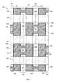
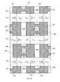
- FIG. 3is a layout diagram of a portion of a non-volatile memory transistor array 300 that implements “H”-shaped source/drain regions in accordance with one embodiment of the present invention.
- the illustrated portion of array 300includes field isolation regions 301 - 308 , control gate/word lines 310 - 312 , source/drain regions 321 - 328 , bit line contacts 331 - 338 , and bit lines 341 - 344 .
- the memory transistor boundariesare defined by dashed lines in FIG. 3 .
- Each of the memory transistorsalso includes a channel region and a floating gate region, which are not explicitly shown in FIG. 3 .
- FIGS. 4A-4Dillustrate array 300 during various stages of fabrication, thereby clarifying the structure of FIG. 3 .
- field isolation regions 301 - 308are initially formed in semiconductor region 401 .
- field isolation regions 301 - 308are preferably shallow trench isolation (STI) regions, but can also be conventional oxide regions formed by the local oxidation of silicon (LOCOS).
- STIshallow trench isolation
- LOCSlocal oxidation of silicon
- control gate/word lines 310 - 312are subsequently formed over the structure of FIG. 4 A.
- oxide-nitride-oxide (ONO) structuresare formed under control gate/word lines 310 - 312 . These ONO structures form floating gate regions of the resulting 2-bit non-volatile memory transistors.
- Source/drain regions 321 - 328are then formed in substrate region 401 .
- Source/drain regions 321 - 328are formed in a self-aligned manner with respect to the control gate/word lines 310 - 312 and field isolation regions 301 - 308 .
- the fabrication of source/drain regions 321 - 328is described in more detail below.
- bit lines 341 - 344are subsequently formed as illustrated in FIG. 3 .
- Bit line 341is connected to contacts 332 and 333 ;
- bit line 342is connected to contacts 331 and 333 ;
- bit line 343is connected to contacts 336 and 338 ; and
- bit line 344is connected to contacts 335 and 337 .
- the 2-bit non-volatile memory transistors formed by the illustrated portion of array 300are shown schematically in FIG. 4D as non-volatile memory transistors H 0,0 to H 2,2 .
- FIG. 5is a more detailed view of the layout of non-volatile memory transistor H 1,1 in accordance with one embodiment of the present invention.
- memory transistor H 1,1assumes that the memory array 300 is fabricated largely in accordance with a conventional 0.35 micron CMOS process flow, with the modifications described below.
- memory transistor H 1,1exhibits a length-to-width ratio of about (1.85 to 2):1, and a layout area on the order of 0.465 microns 2 . Because memory transistor H 1,1 is capable of storing 2-bits of data, the layout density of memory transistor H 1,1 in this example is about 0.2325 microns 2 /bit.
- the length-to-width ratiomay be changed, and the layout area will be reduced.
- FIG. 6is a circuit diagram of a larger portion of memory transistor array 300 .
- Memory transistor array 300implements memory transistors H X,Y , where X and Y represent the row and column locations, respectively, of the memory transistors within memory transistor array 300 .
- memory transistor array 300includes memory transistors H 0,0 -H 3,6 (with the layout of memory transistors H 0,0 -H 2,2 being described above).
- the rowsextend along a first axis, and the columns extend along a second axis, perpendicular to the first axis.
- metal-1 bit lines 341 - 348extend along the second axis of memory transistor array 300 , thereby minimizing the bit line resistance.
- the low bit line resistanceenables memory transistor array 300 to have a large number of columns, while maintaining high-speed access.
- memory transistor array 300can be extended to implement 1K (1024) or more rows.
- Word lines 310 - 313extend along the first axis in the manner described above. Although there are seven columns of memory transistors in the described embodiment, it is understood that other numbers of columns can be used in other embodiments. Additional columns can be added by repeating the pattern defined by memory transistor array 300 .
- the 2-bit memory transistors of memory block 100are accessed through high-voltage select transistors 601 - 608 and metal-2 bit lines 611 - 614 .
- Metal-2 bit lines 611 - 614are located in an interconnect layer that extends over the above-described elements of memory transistor array 300 .
- High-voltage select transistors 601 - 608are designed to have gate oxide sufficient to withstand the high voltages required for programming and erasing the memory transistors.
- select transistors 601 - 608are controlled by select signals S 11 -S 14 to selectively connect metal-2 bit lines 611 - 614 to metal-1 bit lines 341 - 348 .
- Metal-2 bit lines 611 - 614are connected to sense amplifiers and voltage sources during read, program and erase operations in a manner described in more detail below.
- the memory transistors in memory transistor array 300are accessed as follows. Two of the select lines S 11 -S 14 are pulled high, thereby turning on the select transistors coupled to these two select lines, and two of the select lines S 11 -S 14 are pulled low, thereby turning off the select transistors coupled to these two select lines. The turned on select transistors couple two columns of memory transistors to the metal-2 bit lines 611 - 614 .
- FIGS. 7, 8 A, 9 A and 10 Aare cross sectional views of memory transistor H 1,1 along section line A—A of FIG. 5, during various stages of fabrication.
- FIGS. 8B, 9 B, 10 B and 11 - 15are cross sectional views of memory transistor H 1,1 along section line B—B of FIG. 5, during various stages of fabrication.
- the described processis a conventional CMOS twin-well process, except where otherwise noted.
- the field isolation regionsare shallow trench isolation (STI) regions formed by conventional CMOS processing steps. More specifically, STI regions 301 - 308 are created by forming trenches in p-type semiconductor region 401 , and filling the trenches with an insulating material, such as silicon oxide. STI regions 301 - 308 advantageously do not exhibit the bird's beak structure of LOCOS isolation regions. In the described example, STI regions 301 - 308 have a depth in the range of about 1500 to 5000 ⁇ . In a non-preferred embodiment, field isolation regions 301 - 308 can be formed by a LOCOS process, however, the resultant cell size would be much larger.
- STIshallow trench isolation
- a sacrificial oxide(not shown) is grown, and a p-type well implant and a threshold adjusting implant are performed through the sacrificial oxide.
- N-type well regionsare then formed within the substrate. These well regions are not illustrated in the Figures for purposes of clarity. However, it is understood that memory transistor array 300 is fabricated in a p-type well region 401 in the described example. The sacrificial oxide is then removed.
- a lower dielectric layer 801is deposited or created on the surface of p-well region 401 .
- a floating gate layer 802is then deposited on the upper surface of lower dielectric layer 801 .
- an upper dielectric layer 803is either deposited or created on floating gate layer 802 .
- lower dielectric layer 801is a layer of silicon oxide having a thickness in the range of about 10 to 150 Angstroms. In the described embodiment, lower dielectric layer 801 is created by thermally oxidizing the upper surface of semiconductor region 401 at a temperature in the range of 700 to 1300° C.
- floating gate layer 802is a layer of silicon nitride, deposited to a thickness of about 10 to 300 Angstroms over lower dielectric layer 801 .
- Upper dielectric layer 803is a layer of silicon oxide in the described embodiment, whereby lower dielectric layer 801 , floating gate layer 802 and upper dielectric layer 803 form an oxide-nitride-oxide (ONO) layer 804 .
- ONO layer 804is a departure from a conventional CMOS process flow.
- Upper dielectric layer 803can be formed by thermal oxidation of the silicon nitride floating gate layer 802 .
- Silicon nitride layer 802is very stable layer and requires a high temperature in the presence of hydrogen and oxygen to create silicon oxide at a reasonable rate. In one embodiment, this high temperature is in the range 700 to 1300° C.
- silicon nitride layer 802is oxidized until the upper dielectric layer 803 has a thickness in the range of about 10 to 150 Angstroms. This silicon oxide layer promotes charge retention in silicon nitride layer 802 during operation. Oxidization of silicon nitride layer 802 reduces the thickness of silicon nitride layer 802 to approximately 10 to 150 Angstroms.
- upper dielectric layer 803is formed by depositing a layer of silicon oxide over the silicon nitride floating gate layer 802 to a thickness of about 10 to 150 Angstroms (without oxidizing the upper surface of the silicon nitride floating gate layer 802 ).
- upper dielectric layer 803is formed by thermally oxidizing, nitric-oxidizing (e.g., with NO or N 2 O), or nitrogen annealing the upper surface of the silicon nitride floating gate layer 802 at a temperature in the range of 600 to 1300° C., depositing a layer of silicon oxide over the resulting structure, and then thermally oxidizing, nitric-oxidizing (e.g., with NO or N 2 O), or nitrogen annealing the upper surface of the resulting structure at a temperature in the range of 600 to 1300° C.
- thermally oxidizing, nitric-oxidizinge.g., with NO or N 2 O
- nitrogen annealing the upper surface of the resulting structureat a temperature in the range of 600 to 1300° C.
- a blanket layer of polysilicon 901is then deposited over the upper surface of ONO structure 804 .
- phosphorus oxychloridePOCl 3
- Other embodimentsmay implant impurities such as phosphorus and/or arsenic ions to increase the conductivity of polysilicon layer 901 .
- polysilicon layer 901has an n-type conductivity.
- polysilicon layer 901is deposited to a thickness in the range of about 500 to 5000 Angstroms.
- polysilicon layer 901can be doped with a p-type impurity, such as boron, thereby blocking electron injection from the resulting gate electrode 311 during normal operation of the resulting memory transistor H 1,1 .
- a p-type impuritysuch as boron
- a metal silicide layer 902is then formed over the upper surface of polysilicon layer 901 .
- a layer of metal silicidesuch as tungsten silicide, can be deposited directly on polysilicon layer 901 to form metal silicide layer 902 .
- a blanket layer of a refractory metalsuch as titanium or cobalt, is sputtered over the upper surface of polysilicon layer 901 , and subsequently reacted with the underlying polysilicon layer 901 , thereby forming metal silicide layer 902 .
- Photoresist mask 1001is patterned to define the control gate/word line electrodes 311 - 314 of the non-volatile memory transistors H 0,0 -H 3,6 in array 300 (as well as gates of low voltage logic transistors and high voltage logic transistors fabricated on the same chip).
- an etchis then performed to remove the portions of metal silicide layer 902 and polysilicon layer 901 that are exposed by photoresist mask 1001 , thereby forming gate electrodes 310 - 313 .
- this polycide etchis a dry etch.
- polysilicon layer 901is etched until about 20-30 ⁇ are etched from upper dielectric layer 803 .
- Another series of etchesis then performed to remove the exposed portions of ONO layer 804 .
- the portions of upper silicon oxide layer 803 and silicon nitride layer 802 that are exposed by photoresist mask 1001are removed.
- these layersare removed by a two step dry etch, which is performed by a low pressure, high density plasma etcher.
- the first process stepremoves the exposed portions of upper silicon oxide layer 803 .
- the etch timeis calculated to remove all of the exposed portions of upper silicon oxide layer 803 , and part of the underlying silicon nitride layer 802 .
- the second process stepis an isotropic etch that removes the exposed portions of silicon nitride layer 802 .
- the second etchis selective to oxide, thereby protecting the underlying silicon oxide layer 801 .
- the time of the second etchis long enough to assure complete removal of the exposed portions of silicon nitride layer 802 , and the selectivity of the second etch is high enough to assure at least 30-50 ⁇ of lower oxide layer 801 remain.
- the second etchonly partially etches the lower silicon oxide layer 801 . Note that the underlying silicon substrate 401 is not exposed through any part of lower silicon oxide layer 801 .
- the resulting structureis illustrated in FIG. 11 . After these etch steps are completed, photoresist mask 1001 is stripped.
- a first source/drain implant mask(not shown) is then formed over the resulting structure.
- An N-type impuritysuch as arsenic or phosphorous, is then implanted through openings of this first source/drain implant mask.
- arsenicis implanted with a dopant density in the range of 1e14 to 1e16 ions/cm 2 and an implantation energy in the range of 10 to 100 KeV.
- this implant stepis performed at a high implant angle in the range of about 0 to 45 degrees. The high angle implant causes the n-type dopant to extend under the edges of gate electrodes 310 - 313 .
- both arsenic and phosphorouscan be used in the first source/drain implant.
- the implanted N-type impuritiesare illustrated as N type source/drain regions 1201 and 1202 in FIG. 12 . These regions are self-aligned with gate electrode 311 .
- p-type implantscan also be performed through the first source/drain implant mask. More specifically, a P-type impurity, such as boron (B) or Boron Fluoride (BF 2 ), can be implanted at angles from 0 to 45 degrees. In accordance with one embodiment of the present invention, the P-type impurities are implanted with a dopant density in the range of 5e12 to 1e15 ions/cm 2 , depending on the implantation energy, which is in the range of 10 to 100 KeV. The implanted boron serves to adjust the threshold voltages of the non-volatile memory transistors in array 300 . Such implanted p-type impurities are represented by p-type regions 1211 and 1212 in FIG. 12 .
- sidewall spacersare formed by depositing a thin dielectric layer over the resulting structure, and a thick layer of spacer dielectric material over the thin dielectric layer. The spacer dielectric material is then etched back to form dielectric spacers adjacent to the sidewalls of the gate electrodes 310 - 313 .
- the resulting sidewall spacers 1301 - 1302 and corresponding thin dielectric layers 1311 - 1312are illustrated in FIG. 13 .
- the thin dielectric layers 1311 - 1312are silicon nitride and the sidewall spacers 1301 - 1302 are silicon oxide.
- the thin dielectric layers 1311 - 1312are silicon oxide, and the sidewall spacers 1301 - 1302 are silicon nitride. In yet other embodiments, the thin dielectric layers 1311 - 1312 are omitted, and the sidewall spacers 1301 - 1302 can be either silicon oxide or silicon nitride.
- an second source/drain implant mask(not shown) is formed over the resulting structure.
- An N+ implantis then performed by implanting an N-type impurity, such as arsenic or phosphorous, through the second source/drain implant mask, thereby forming N+ type source/drain regions 1401 - 1402 (FIG. 14 ).
- arsenicis implanted with a dopant density in the range of 1e15 to 1e16 ions/cm 2 and an implantation energy in the range of 10 to 100 KeV.
- both arsenic and phosphorouscan be used in the N+ implant.
- first source/drain regions 1201 - 1202 and second source/drain regions 1401 - 1402are activated, thereby forming source/drain regions 323 and 326 as illustrated in FIG. 15 .
- the left and right charge trapping regions 15 L and 15 R in floating gate layer 802 of memory transistor H 1,1are also illustrated in dashed lines in FIG. 15 .
- metal silicide layer 902is not formed over polysilicon layer 902 in the manner described above in connection with FIGS. 9A and 9B. Instead, processing is performed as described above in connection with FIGS. 6-14, but without forming metal silicide layer 902 .
- the resulting structureis illustrated in FIG. 16, wherein similar elements in FIGS. 14 and 16 are labeled with similar reference numbers.
- a blanket layer of a refractory metalsuch as titanium and/or cobalt, is blanket deposited over the structure of FIG. 16, thereby forming refractory metal layer 1701 .
- An annealis then performed, thereby causing refractory metal layer 1701 to react with underlying silicon regions to form metal silicide regions.
- the annealcauses metal silicide regions 1801 , 1802 and 1803 to be formed over source/drain region 326 , source/drain region 323 and polysilicon gate electrode 901 , respectively.
- the portions of refractory metal layer 1701 which overlie sidewall spacers 1301 and 1302remain unreacted.
- This annealalso helps to activate the impurities previously implanted in p-well region 401 .
- a refractory metal etching stepremoves the un-reacted portions of refractory metal layer 1701 thereby leaving self-aligned silicide (i.e., salicide) regions 1801 - 1803 , as illustrated in FIG. 18 .
- the right charge trapping region 15 R of memory transistor H 1,1is programmed in the following manner.
- Word line 311is held at a programming voltage of 5-15 Volts, while the word lines 310 , 312 and 313 associated with non-selected memory transistors are held at a voltage of 0 Volts.
- Source/drain region 323 of memory transistor H 1,1is maintained at a voltage of 3-10 Volts, and source/drain region 326 of memory transistor H 1,1 is maintained at a voltage of 0 Volts. Under these conditions, charge is stored in right charge trapping region 15 R by hot electron injection.
- the duration of the programming operationis on the order of microseconds. Note that the duration of the programming operation is not long enough and the applied source/drain voltage of 3-10 Volts is not high enough to cause the non-selected memory transistors to be erased during the programming operation.
- the left charge trapping region 15 L of memory transistor H 1,1is programmed in a similar manner. More specifically, word line 311 is held at a programming voltage of 5-15 Volts, while the word lines 310 , 312 and 313 associated with non-selected memory transistors are held at a voltage of 0 Volts. Source/drain region 323 of memory transistor H 1,1 is maintained at a voltage of 0 Volts, and source/drain region 326 of memory transistor H 1,1 is maintained at a voltage of 3-10 Volts. Under these conditions, charge is stored in left charge trapping region 15 L by hot electron injection. Note that the insulating nature of silicon nitride layer separately maintains the charges stored in the left and right charge trapping regions 15 L and 15 R.
- the right charge trapping region 15 R of memory transistor H 1,1is read as follows.
- the word line 311is maintained at a read voltage of 1.5-5 Volts, while the word lines 310 , 312 and 313 are held at a voltage of 0 Volts.
- Source/drain region 326is held at a voltage of 0.5-2 Volts, and source/drain region 323 is coupled to a sense amplifier (and held at a voltage of about 0 Volts), such that a reverse read condition exists for the right charge trapping region 15 R of memory transistor H 1,1 . Under these conditions, the non-selected memory transistors are neither read nor disturbed.
- the left charge trapping region of memory transistor H 1,1is read in a similar manner.
- Word line 311is maintained at a read voltage of 1.5-5 Volts, while the word lines 310 , 312 and 313 are held at a voltage of 0 Volts.
- Source/drain region 323is held at a voltage of 0.5-2 Volts, and source/drain region 326 is coupled to a sense amplifier (and held at a voltage of about 0 Volts), such that a reverse read condition exists for the left charge trapping region 15 L of memory transistor H 1,1 .
- Memory array 300is erased as follows. A voltage of 0 to ⁇ 10 Volts is applied to all of the word lines 310 - 313 of memory transistor array 300 , and an erase voltage of 10 to 0 Volts is applied to all of the bit lines 341 - 348 (by turning on all of select transistors 601 - 608 ). These erase voltages are selected such that charge is removed from all of the charge trapping regions in memory transistors H 0,0 -H 3,6 , thereby erasing these memory transistors.
- Memory transistor array 300exhibits the following advantages. First, memory transistor array 300 exhibits a relatively low source/drain series resistance because the source/drain regions are relatively small (when compared with the diffusion bit lines of memory block 100 ). Memory transistor array 300 also exhibits a relatively low bit line resistance when compared with the diffusion bit lines of memory block 100 . This enables memory transistor array 300 to have a relatively large number of rows.
- Memory transistors H 0,0 -H 3,6also advantageously exhibit a relatively shallow source/drain junction depth (e.g., less than 0.1 microns), because these memory transistors are fabricated largely in accordance with conventional CMOS processing techniques (and do not have the requirement of extending under a bit line oxide region 124 , as in memory block 100 ).
- Memory transistors H 0,0 -H 3,6are also advantageously able to implement self-aligned salicide on both the word lines 310 - 313 and the source/drain regions 321 - 328 , when implementing the embodiment illustrated by FIGS. 16-18.
- the use of self-aligned salicideresults in low RC delay and high-speed operation.
- field isolation regionsare used to isolate the H-shaped source/drain regions, there is minimal leakage between adjacent source/drain regions in memory transistor array 300 .
Landscapes
- Semiconductor Memories (AREA)
Abstract
Description
The present invention relates to non-volatile memory transistors. More specifically, the present invention relates to a method and structure of using a 2-bit non-volatile memory transistor to form a flash memory transistor array.
A 2-bit non-volatile semiconductor memory transistor has been described in U.S. Pat. No. 5,768,192, to Eitan. However, the manners of using 2-bit NVM transistors in a memory array have not yet been fully developed.
One memory array that implements 2-bit NVM transistors is described in U.S. Pat. No. 6,181,597 to Nachumovsky.
FIG. 1 is a schematic diagram illustrating aconventional memory block 100.Memory block 100 implements uses a plurality of 2-bit memory transistors, which are identified as memory transistors MX,Y, where X and Y represent the row and column locations, respectively, of the memory transistors withinmemory block 100. Thus,memory block 100 includes memory transistors M0,0-M3,6. The rows extend along a first axis, and the columns extend along a second axis, perpendicular to the first axis.
Each of the memory transistors M0,0-M3,6includes two charge trapping regions, namely, a left charge trapping region and a right charge trapping region, thereby enabling each of memory transistors M0,0-M3,6to store 2-bits of data.
The source and drain regions of memory transistors M0,0-M3,6are formed by diffused regions101-108, which extend in parallel along the second axis. Diffused regions101-108 also operate as bit lines withinmemory block 100. Thus, diffused regions101-108 are referred to as diffusion bit lines.
ONO structures111-117 are located between adjacent diffusion bit lines101-108, as illustrated. The gates of the memory transistors in each row are commonly connected to a word line. More specifically, the memory transistors of rows0-3 are connected to word lines WL0-WL3, respectively.
The 2-bit memory transistors ofmemory block 100 are accessed through high-voltage select transistors131-138 and metal bit lines141-144. Metal bit lines141-144 are located in an interconnect layer that extends over the above-described elements ofmemory block 100. High-voltage select transistors131-138 are designed to have gate oxide sufficient to withstand the high voltages required for programming and erasing the memory transistors. In general, select transistors131-138 are controlled to selectively connect metal bit lines141-144 to diffusion bit lines101-108.
FIG. 2 is a cross sectional view of memory transistors M0,0and M0,1along the first axis through word line WL0. Diffusion bit lines101-103 are n-type regions formed in a p-typesilicon semiconductor region 110. Bitline oxide regions 124 are formed over the diffusion bit lines101-103. Because the memory transistors inmemory block 100 do not require field oxide for isolation,memory block 100 can be referred to as a fieldless array.ONO structures line insulating regions 124, diffusion bit lines101-103 andsubstrate 110 in the manner illustrated. Word line WL0is a polycide or salicide structure that includes a layer of conductively dopedpolycrystalline silicon 126 and an overlying layer ofmetal silicide 127, and extends overONO structures 111 and112 (and bit line insulating regions124). Word lines WL0forms the control gate of memory transistors M0,0and M0,1. The fabrication ofmemory block 100 is described in U.S. Pat. No. 6,346,442 by Aloni et al.
Typical problems associated withmemory block 100 and the corresponding memory transistors include (1) relatively large source/drain series resistances due to the use of diffusion bit lines, (2) relatively deep source/drain junction depths due to the high thermal budget required by bit line oxidate regions, (3) an unadaptable structure with respect to advanced CMOS technology using self-aligned salicidation process (i.e., almost impossible to implement self-aligned salicide on word lines and source/drain regions), and (4) high bit line-to-bit line leakage, because the memory transistors are separated by active regions, without any general isolation structure.
It would therefore be desirable to have a flash memory array structure that implements 2-bit non-volatile memory transistors and exhibits a relatively low source/drain series resistance, and a relatively low bit line resistance. It would further be desirable if the source/drain junction depth of the memory transistors in the array are relatively shallow (e.g., less than 0.1 microns). It would further be desirable if the flash memory array structure were capable of implementing a self-aligned salicidation process over both the gate and source/drain regions of the array. It would also be desirable if there were no leakage issues between bit lines of the flash memory array. It would further be desirable if the flash memory array exhibits low word line capacitance, thereby resulting in low RC delay and high-speed operation.
Accordingly, the present invention provides an improved array structure for implementing a flash memory array using 2-bit non-volatile memory transistors. For purposes of this disclosure, a flash memory array is defined as a non-volatile memory array that cannot be erased on a word-by-word basis, but which must be erased in blocks. The present invention also provides a method for fabricating this improved array structure, which is largely compatible with a conventional CMOS process flow.
In accordance with one embodiment, a non-volatile memory (NVM) array is fabricated with a plurality of 2-bit NVM transistors arranged in a plurality of rows extending along a first axis, and a plurality of columns extending along a second axis, perpendicular to the first axis. The non-volatile memory array includes a plurality of field isolation regions located in a semiconductor substrate. In a preferred embodiment, the field isolation regions are shallow trench isolation (STI) regions.
A plurality of word lines extend over the semiconductor substrate along the first axis, wherein the word lines also form control gates of the 2-bit NVM transistors. Oxide-nitride-oxide (ONO) structures are located between the substrate and the word lines, wherein the nitride layer of the ONO structures provides floating gate storage for the NVM transistors. A plurality of H-shaped source/drain regions are defined by the field isolation regions and the word lines, wherein each source/drain region serves as a source/drain for four different NVM transistors in the array. Self-aligned silicide can be formed over both the word lines and the source/drain regions.
Because each source/drain region only serves as a source/drain region for four different NVM transistors (and not an entire diffusion bit line), the array structure of the present invention advantageously provides a low source/drain series resistance and relatively low bit line resistances.
The present invention also includes a method of fabricating an array of 2-bit NVM cells, wherein the method includes (1) forming a plurality of field isolation regions in a semiconductor substrate, (2) forming a lower dielectric layer over the semiconductor substrate, (3) forming a floating gate dielectric layer over the lower dielectric layer, (4) forming an upper dielectric layer over the floating gate dielectric layer, (5) forming a gate electrode layer over the upper dielectric layer, (6) patterning the gate electrode layer, the upper dielectric layer and the floating gate dielectric layer, wherein the gate electrode layer is patterned to form a plurality of word line/control gate structures extending along a first axis, and wherein the floating gate dielectric layer is patterned to form a plurality of floating gate structures, and (7) forming H-shaped source/drain regions having a first conductivity type in the substrate, the H-shaped source/drain regions being defined by the word line/control gate structures and field isolation regions.
In one embodiment, the lower dielectric layer is formed by thermally oxidizing the upper surface of the substrate. The floating gate dielectric layer can be formed by depositing a silicon nitride layer over the lower dielectric layer. The upper dielectric layer can be formed by thermally oxidizing the upper surface of the floating gate dielectric layer and/or depositing a silicon oxide layer over the floating gate dielectric layer.
The gate electrode layer can be formed by depositing a polysilicon layer over the upper dielectric layer. The polysilicon layer can be doped to the first conductivity type or a second conductivity type, opposite the first conductivity type. A refractory metal layer or a metal silicide layer can be deposited over the polysilicon layer, thereby forming a polycide gate electrode. In another embodiment, self-aligned salicide regions are formed over both the word line/control gate structures and the source/drain regions.
The source/drain regions are fabricated in accordance with conventional processing techniques, and are not required to extend under bit line oxidation in the manner illustrated in FIG. 2 above. As a result, the source/drain junction depth of the NVM transistors in the array are advantageously relatively shallow.
The present invention will be more fully understood in view of the following description and drawings.
FIG. 1 is a circuit diagram of a conventional memory block that uses 2-bit non-volatile memory transistors.
FIG. 2 is a cross sectional view of selected memory transistors of FIG. 1, taken along a word line.
FIG. 3 is a layout diagram of a portion of a non-volatile memory transistor array that implements “H”-shaped source/drain regions in accordance with one embodiment of the present invention.
FIGS. 4A-4D are layout diagrams illustrating the array of FIG. 3 during various stages of fabrication.
FIG. 5 is detailed layout diagram of a single non-volatile memory transistor in the array of FIG. 3 in accordance with one embodiment of the present invention.
FIG. 6 is a circuit diagram of a larger portion of the memory transistor array of FIG.3.
FIGS. 7,8A,9A and10A are cross sectional views of the non-volatile memory transistor of FIG. 5, along section line A—A, during various stages of fabrication.
FIGS. 8B,9B,10B and11-15 are cross sectional views the non-volatile memory transistor of FIG. 5, along section line B—B, during various stages of fabrication.
FIGS. 16-18 are cross sectional views the non-volatile memory transistor of FIG. 5, along section line B—B, during various stages of fabrication, when self-aligned salicide is formed over both the word line/control gate and source/drain regions of the non-volatile memory transistor.
FIG. 3 is a layout diagram of a portion of a non-volatilememory transistor array 300 that implements “H”-shaped source/drain regions in accordance with one embodiment of the present invention. The illustrated portion ofarray 300 includes field isolation regions301-308, control gate/word lines310-312, source/drain regions321-328, bit line contacts331-338, and bit lines341-344. The memory transistor boundaries are defined by dashed lines in FIG.3. Each of the memory transistors also includes a channel region and a floating gate region, which are not explicitly shown in FIG.3.
FIGS. 4A-4D illustratearray 300 during various stages of fabrication, thereby clarifying the structure of FIG.3. As illustrated in FIG. 4A, field isolation regions301-308 are initially formed insemiconductor region 401. As described in more detail below, field isolation regions301-308 are preferably shallow trench isolation (STI) regions, but can also be conventional oxide regions formed by the local oxidation of silicon (LOCOS).
As illustrated in FIG. 4B, control gate/word lines310-312 are subsequently formed over the structure of FIG.4A. As described in more detail below, oxide-nitride-oxide (ONO) structures are formed under control gate/word lines310-312. These ONO structures form floating gate regions of the resulting 2-bit non-volatile memory transistors.
As illustrated in FIG. 4C, the source/drain regions321-328 are then formed insubstrate region 401. Source/drain regions321-328 are formed in a self-aligned manner with respect to the control gate/word lines310-312 and field isolation regions301-308. The fabrication of source/drain regions321-328 is described in more detail below.
As illustrated in FIG. 4D, the source/drain contacts331-338 are subsequently formed, thereby providing connections to source/drain regions321-328, respectively. Bit lines341-344 are subsequently formed as illustrated in FIG.3.Bit line 341 is connected tocontacts bit line 342 is connected tocontacts bit line 343 is connected tocontacts line 344 is connected tocontacts array 300, are shown schematically in FIG. 4D as non-volatile memory transistors H0,0to H2,2.
FIG. 5 is a more detailed view of the layout of non-volatile memory transistor H1,1in accordance with one embodiment of the present invention. This example assumes that thememory array 300 is fabricated largely in accordance with a conventional 0.35 micron CMOS process flow, with the modifications described below. In the described example, memory transistor H1,1exhibits a length-to-width ratio of about (1.85 to 2):1, and a layout area on the order of 0.465 microns2. Because memory transistor H1,1is capable of storing 2-bits of data, the layout density of memory transistor H1,1in this example is about 0.2325 microns2/bit. However, if memory transistor H1,1is fabricated using CMOS processes having smaller minimum line widths, the length-to-width ratio may be changed, and the layout area will be reduced.
FIG. 6 is a circuit diagram of a larger portion ofmemory transistor array 300.Memory transistor array 300 implements memory transistors HX,Y, where X and Y represent the row and column locations, respectively, of the memory transistors withinmemory transistor array 300. Thus,memory transistor array 300 includes memory transistors H0,0-H3,6(with the layout of memory transistors H0,0-H2,2being described above). The rows extend along a first axis, and the columns extend along a second axis, perpendicular to the first axis.
Advantageously, metal-1 bit lines341-348 extend along the second axis ofmemory transistor array 300, thereby minimizing the bit line resistance. The low bit line resistance enablesmemory transistor array 300 to have a large number of columns, while maintaining high-speed access. For example,memory transistor array 300 can be extended to implement 1K (1024) or more rows.
Word lines310-313 extend along the first axis in the manner described above. Although there are seven columns of memory transistors in the described embodiment, it is understood that other numbers of columns can be used in other embodiments. Additional columns can be added by repeating the pattern defined bymemory transistor array 300.
The 2-bit memory transistors ofmemory block 100 are accessed through high-voltage select transistors601-608 and metal-2 bit lines611-614. Metal-2 bit lines611-614 are located in an interconnect layer that extends over the above-described elements ofmemory transistor array 300. High-voltage select transistors601-608 are designed to have gate oxide sufficient to withstand the high voltages required for programming and erasing the memory transistors. In general, select transistors601-608 are controlled by select signals S11-S14to selectively connect metal-2 bit lines611-614 to metal-1 bit lines341-348. Metal-2 bit lines611-614 are connected to sense amplifiers and voltage sources during read, program and erase operations in a manner described in more detail below.
The memory transistors inmemory transistor array 300 are accessed as follows. Two of the select lines S11-S14are pulled high, thereby turning on the select transistors coupled to these two select lines, and two of the select lines S11-S14are pulled low, thereby turning off the select transistors coupled to these two select lines. The turned on select transistors couple two columns of memory transistors to the metal-2 bit lines611-614.
The fabrication of memory transistors will now be described. FIGS. 7,8A,9A and10A are cross sectional views of memory transistor H1,1along section line A—A of FIG. 5, during various stages of fabrication. FIGS. 8B,9B,10B and11-15 are cross sectional views of memory transistor H1,1along section line B—B of FIG. 5, during various stages of fabrication. The described process is a conventional CMOS twin-well process, except where otherwise noted.
As illustrated in FIG. 7, the field isolation regions, includingfield isolation regions type semiconductor region 401, and filling the trenches with an insulating material, such as silicon oxide. STI regions301-308 advantageously do not exhibit the bird's beak structure of LOCOS isolation regions. In the described example, STI regions301-308 have a depth in the range of about 1500 to 5000 Å. In a non-preferred embodiment, field isolation regions301-308 can be formed by a LOCOS process, however, the resultant cell size would be much larger.
After field isolation regions301-308 are formed, a sacrificial oxide (not shown) is grown, and a p-type well implant and a threshold adjusting implant are performed through the sacrificial oxide. N-type well regions are then formed within the substrate. These well regions are not illustrated in the Figures for purposes of clarity. However, it is understood thatmemory transistor array 300 is fabricated in a p-type well region 401 in the described example. The sacrificial oxide is then removed.
As illustrated in FIGS. 8A and 8B, after STI regions301-308 have been formed, a lowerdielectric layer 801 is deposited or created on the surface of p-well region 401. A floatinggate layer 802 is then deposited on the upper surface of lowerdielectric layer 801. Then, anupper dielectric layer 803 is either deposited or created on floatinggate layer 802.
In the described embodiment, lowerdielectric layer 801 is a layer of silicon oxide having a thickness in the range of about 10 to 150 Angstroms. In the described embodiment, lowerdielectric layer 801 is created by thermally oxidizing the upper surface ofsemiconductor region 401 at a temperature in the range of 700 to 1300° C.
In the described embodiment, floatinggate layer 802 is a layer of silicon nitride, deposited to a thickness of about 10 to 300 Angstroms over lowerdielectric layer 801.
Upperdielectric layer 803 is a layer of silicon oxide in the described embodiment, whereby lowerdielectric layer 801, floatinggate layer 802 andupper dielectric layer 803 form an oxide-nitride-oxide (ONO)layer 804. The formation ofONO layer 804 is a departure from a conventional CMOS process flow. Upperdielectric layer 803 can be formed by thermal oxidation of the silicon nitride floatinggate layer 802.Silicon nitride layer 802 is very stable layer and requires a high temperature in the presence of hydrogen and oxygen to create silicon oxide at a reasonable rate. In one embodiment, this high temperature is in the range 700 to 1300° C. In this embodiment,silicon nitride layer 802 is oxidized until theupper dielectric layer 803 has a thickness in the range of about 10 to 150 Angstroms. This silicon oxide layer promotes charge retention insilicon nitride layer 802 during operation. Oxidization ofsilicon nitride layer 802 reduces the thickness ofsilicon nitride layer 802 to approximately 10 to 150 Angstroms.
In one variation,upper dielectric layer 803 is formed by depositing a layer of silicon oxide over the silicon nitride floatinggate layer 802 to a thickness of about 10 to 150 Angstroms (without oxidizing the upper surface of the silicon nitride floating gate layer802). In another variation,upper dielectric layer 803 is formed by thermally oxidizing, nitric-oxidizing (e.g., with NO or N2O), or nitrogen annealing the upper surface of the silicon nitride floatinggate layer 802 at a temperature in the range of 600 to 1300° C., depositing a layer of silicon oxide over the resulting structure, and then thermally oxidizing, nitric-oxidizing (e.g., with NO or N2O), or nitrogen annealing the upper surface of the resulting structure at a temperature in the range of 600 to 1300° C.
As illustrated in FIGS. 9A and 9B, a blanket layer ofpolysilicon 901 is then deposited over the upper surface ofONO structure 804. In some embodiments, phosphorus oxychloride (POCl3) is used todope polysilicon layer 901 to increase the conductivity ofpolysilicon layer 901. Other embodiments may implant impurities such as phosphorus and/or arsenic ions to increase the conductivity ofpolysilicon layer 901. In these embodiments,polysilicon layer 901 has an n-type conductivity. In one embodiment,polysilicon layer 901 is deposited to a thickness in the range of about 500 to 5000 Angstroms.
In yet another embodiment,polysilicon layer 901 can be doped with a p-type impurity, such as boron, thereby blocking electron injection from the resultinggate electrode 311 during normal operation of the resulting memory transistor H1,1.
In accordance with the present embodiment, ametal silicide layer 902 is then formed over the upper surface ofpolysilicon layer 901. A layer of metal silicide, such as tungsten silicide, can be deposited directly onpolysilicon layer 901 to formmetal silicide layer 902. In an alternate embodiment, a blanket layer of a refractory metal, such as titanium or cobalt, is sputtered over the upper surface ofpolysilicon layer 901, and subsequently reacted with theunderlying polysilicon layer 901, thereby formingmetal silicide layer 902.
A layer of photoresist is then deposited over the resulting structure. This photoresist layer is exposed and developed to formphotoresist mask 1001, as illustrated in FIGS. 10A and 10B.Photoresist mask 1001 is patterned to define the control gate/word line electrodes311-314 of the non-volatile memory transistors H0,0-H3,6in array300 (as well as gates of low voltage logic transistors and high voltage logic transistors fabricated on the same chip).
As illustrated in FIG. 11, an etch is then performed to remove the portions ofmetal silicide layer 902 andpolysilicon layer 901 that are exposed byphotoresist mask 1001, thereby forming gate electrodes310-313. In one embodiment, this polycide etch is a dry etch. In the described embodiment,polysilicon layer 901 is etched until about 20-30 Å are etched fromupper dielectric layer 803.
Another series of etches is then performed to remove the exposed portions ofONO layer 804. The portions of uppersilicon oxide layer 803 andsilicon nitride layer 802 that are exposed byphotoresist mask 1001 are removed. In one embodiment, these layers are removed by a two step dry etch, which is performed by a low pressure, high density plasma etcher. The first process step removes the exposed portions of uppersilicon oxide layer 803. The etch time is calculated to remove all of the exposed portions of uppersilicon oxide layer 803, and part of the underlyingsilicon nitride layer 802. The second process step is an isotropic etch that removes the exposed portions ofsilicon nitride layer 802. The second etch is selective to oxide, thereby protecting the underlyingsilicon oxide layer 801. The time of the second etch is long enough to assure complete removal of the exposed portions ofsilicon nitride layer 802, and the selectivity of the second etch is high enough to assure at least 30-50 Å oflower oxide layer 801 remain. The second etch only partially etches the lowersilicon oxide layer 801. Note that theunderlying silicon substrate 401 is not exposed through any part of lowersilicon oxide layer 801. The resulting structure is illustrated in FIG.11. After these etch steps are completed,photoresist mask 1001 is stripped.
A first source/drain implant mask (not shown) is then formed over the resulting structure. An N-type impurity, such as arsenic or phosphorous, is then implanted through openings of this first source/drain implant mask. In one embodiment, arsenic is implanted with a dopant density in the range of 1e14 to 1e16 ions/cm2and an implantation energy in the range of 10 to 100 KeV. In one variation, this implant step is performed at a high implant angle in the range of about 0 to 45 degrees. The high angle implant causes the n-type dopant to extend under the edges of gate electrodes310-313. In another variation, both arsenic and phosphorous can be used in the first source/drain implant. The implanted N-type impurities are illustrated as N type source/drain regions gate electrode 311.
In one variation, p-type implants can also be performed through the first source/drain implant mask. More specifically, a P-type impurity, such as boron (B) or Boron Fluoride (BF2), can be implanted at angles from 0 to 45 degrees. In accordance with one embodiment of the present invention, the P-type impurities are implanted with a dopant density in the range of 5e12 to 1e15 ions/cm2, depending on the implantation energy, which is in the range of 10 to 100 KeV. The implanted boron serves to adjust the threshold voltages of the non-volatile memory transistors inarray 300. Such implanted p-type impurities are represented by p-type regions
After the first source/drain implants have been performed, sidewall spacers are formed by depositing a thin dielectric layer over the resulting structure, and a thick layer of spacer dielectric material over the thin dielectric layer. The spacer dielectric material is then etched back to form dielectric spacers adjacent to the sidewalls of the gate electrodes310-313. The resulting sidewall spacers1301-1302 and corresponding thin dielectric layers1311-1312 are illustrated in FIG.13. In one embodiment, the thin dielectric layers1311-1312 are silicon nitride and the sidewall spacers1301-1302 are silicon oxide. In another embodiment, the thin dielectric layers1311-1312 are silicon oxide, and the sidewall spacers1301-1302 are silicon nitride. In yet other embodiments, the thin dielectric layers1311-1312 are omitted, and the sidewall spacers1301-1302 can be either silicon oxide or silicon nitride.
After sidewall spacers1301-1302 have been formed, an second source/drain implant mask (not shown) is formed over the resulting structure. An N+ implant is then performed by implanting an N-type impurity, such as arsenic or phosphorous, through the second source/drain implant mask, thereby forming N+ type source/drain regions1401-1402 (FIG.14). In one embodiment, arsenic is implanted with a dopant density in the range of 1e15 to 1e16 ions/cm2and an implantation energy in the range of 10 to 100 KeV. In one variation, both arsenic and phosphorous can be used in the N+ implant.
After the N+ implant has been performed, conventional back end processes (inter-metal layer and contact formation) are performed, thereby forming contacts, such as contacts331-338, metal-1 lines, such as metal-1 bit lines341-348 and metal-2 lines, such as metal-2 bit lines611-614. Annealing steps performed during various stages of the process cause first source/drain regions1201-1202 and second source/drain regions1401-1402 to be activated, thereby forming source/drain regions charge trapping regions gate layer 802 of memory transistor H1,1are also illustrated in dashed lines in FIG.15.
In an alternate embodiment of the present invention,metal silicide layer 902 is not formed overpolysilicon layer 902 in the manner described above in connection with FIGS. 9A and 9B. Instead, processing is performed as described above in connection with FIGS. 6-14, but without formingmetal silicide layer 902. The resulting structure is illustrated in FIG. 16, wherein similar elements in FIGS. 14 and 16 are labeled with similar reference numbers.
As illustrated in FIG. 17, a blanket layer of a refractory metal, such as titanium and/or cobalt, is blanket deposited over the structure of FIG. 16, thereby formingrefractory metal layer 1701. An anneal is then performed, thereby causingrefractory metal layer 1701 to react with underlying silicon regions to form metal silicide regions. Thus, the anneal causesmetal silicide regions drain region 326, source/drain region 323 andpolysilicon gate electrode 901, respectively. The portions ofrefractory metal layer 1701 which overliesidewall spacers well region 401. A refractory metal etching step removes the un-reacted portions ofrefractory metal layer 1701 thereby leaving self-aligned silicide (i.e., salicide) regions1801-1803, as illustrated in FIG.18.
The operation of memory transistor H1,1will now be described.
The rightcharge trapping region 15R of memory transistor H1,1is programmed in the following manner.Word line 311 is held at a programming voltage of 5-15 Volts, while the word lines310,312 and313 associated with non-selected memory transistors are held at a voltage of 0 Volts. Source/drain region 323 of memory transistor H1,1is maintained at a voltage of 3-10 Volts, and source/drain region 326 of memory transistor H1,1is maintained at a voltage of 0 Volts. Under these conditions, charge is stored in rightcharge trapping region 15R by hot electron injection. The duration of the programming operation is on the order of microseconds. Note that the duration of the programming operation is not long enough and the applied source/drain voltage of 3-10 Volts is not high enough to cause the non-selected memory transistors to be erased during the programming operation.
The leftcharge trapping region 15L of memory transistor H1,1is programmed in a similar manner. More specifically,word line 311 is held at a programming voltage of 5-15 Volts, while the word lines310,312 and313 associated with non-selected memory transistors are held at a voltage of 0 Volts. Source/drain region 323 of memory transistor H1,1is maintained at a voltage of 0 Volts, and source/drain region 326 of memory transistor H1,1is maintained at a voltage of 3-10 Volts. Under these conditions, charge is stored in leftcharge trapping region 15L by hot electron injection. Note that the insulating nature of silicon nitride layer separately maintains the charges stored in the left and rightcharge trapping regions
The rightcharge trapping region 15R of memory transistor H1,1is read as follows. Theword line 311 is maintained at a read voltage of 1.5-5 Volts, while the word lines310,312 and313 are held at a voltage of 0 Volts. Source/drain region 326 is held at a voltage of 0.5-2 Volts, and source/drain region 323 is coupled to a sense amplifier (and held at a voltage of about 0 Volts), such that a reverse read condition exists for the rightcharge trapping region 15R of memory transistor H1,1. Under these conditions, the non-selected memory transistors are neither read nor disturbed.
The left charge trapping region of memory transistor H1,1is read in a similar manner.Word line 311 is maintained at a read voltage of 1.5-5 Volts, while the word lines310,312 and313 are held at a voltage of 0 Volts. Source/drain region 323 is held at a voltage of 0.5-2 Volts, and source/drain region 326 is coupled to a sense amplifier (and held at a voltage of about 0 Volts), such that a reverse read condition exists for the leftcharge trapping region 15L of memory transistor H1,1.
Memory transistors H0,0-H3,6also advantageously exhibit a relatively shallow source/drain junction depth (e.g., less than 0.1 microns), because these memory transistors are fabricated largely in accordance with conventional CMOS processing techniques (and do not have the requirement of extending under a bitline oxide region 124, as in memory block100).
Memory transistors H0,0-H3,6are also advantageously able to implement self-aligned salicide on both the word lines310-313 and the source/drain regions321-328, when implementing the embodiment illustrated by FIGS. 16-18. The use of self-aligned salicide results in low RC delay and high-speed operation.
Moreover, because field isolation regions are used to isolate the H-shaped source/drain regions, there is minimal leakage between adjacent source/drain regions inmemory transistor array 300.
These advantages enable the memory transistor of the present invention to be aggressively scaled (shrunk), thereby providing for a more adaptable and embeddable memory transistor in advanced CMOS technology.
Although the invention has been described in connection with several embodiments, it is understood that this invention is not limited to the embodiments disclosed, but is capable of various modifications which would be apparent to a person skilled in the art. Thus, the invention is limited only by the following claims.
Claims (17)
1. A method of fabricating an array of 2-bit non-volatile memory cells, the method comprising:
forming a plurality of field isolation regions in a semiconductor substrate;
forming a lower dielectric layer over the semiconductor substrate;
forming a floating gate dielectric layer over the lower dielectric layer;
forming an upper dielectric layer over the floating gate dielectric layer;
forming a gate electrode layer over the upper dielectric layer;
patterning the gate electrode layer, the upper dielectric layer and the floating gate dielectric layer, wherein the gate electrode layer is patterned to form a plurality of word line/control gate structures extending along a first axis, and wherein the floating gate dielectric layer is patterned to form a plurality of floating gate structures; and
forming H-shaped source/drain regions in the substrate, in alignment with the word line/control gate structures and field isolation regions, the H-shaped source/drain regions having a first conductivity type.
2. The method ofclaim 1 , wherein the step of forming the field isolation regions comprises:
forming trenches in the substrate; and
filling the trenches with an insulating material.
3. The method ofclaim 1 , wherein the step of forming the field isolation regions comprises performing local oxidation of silicon (LOCOS) within the substrate.
4. The method ofclaim 1 , wherein the step of forming the lower dielectric layer comprises thermally oxidizing an upper surface of the substrate.
5. The method ofclaim 1 , wherein the step of forming the floating gate dielectric layer comprises depositing a silicon nitride layer over the lower dielectric layer.
6. The method ofclaim 5 , wherein the step of forming the upper dielectric layer comprises thermally oxidizing an upper surface of the floating gate dielectric layer.
7. The method ofclaim 6 , wherein the step of forming the upper dielectric layer further comprises depositing a silicon oxide layer over the floating gate dielectric layer.
8. The method ofclaim 1 , wherein the step of forming the gate electrode layer comprises depositing a polysilicon layer over the upper dielectric layer.
9. The method ofclaim 8 , further comprising doping the polysilicon layer to have the first conductivity type.
10. The method ofclaim 8 , further comprising doping the polysilicon layer to have a second conductivity type, opposite the first conductivity type.
11. The method ofclaim 8 , wherein the step of forming the gate electrode layer further comprises depositing a refractory metal silicide layer over the polysilicon layer.
12. The method ofclaim 8 , wherein the step of forming the gate electrode layer further comprises depositing a refractory metal layer over the polysilicon layer.
13. The method ofclaim 1 , wherein the step of forming the H-shaped source drain regions comprises:
performing a first source/drain implant of the first conductivity type into the substrate in alignment with the word line/control gate structures and field isolation regions;
forming sidewall spacers adjacent to the word line/control gate structures; and then
performing a second source/drain implant of the first conductivity type into the substrate in alignment with the sidewall spacers and the field isolation regions.
14. The method ofclaim 13 , wherein the first source/drain implant is performed at a tilt angle greater than 0 degrees.
15. The method ofclaim 13 , further comprising implanting an impurity having a second conductivity type, opposite the first conductivity type, into the substrate in alignment with the word line/control gate structures and field isolation regions.
16. The method ofclaim 15 , wherein the impurity having the second conductivity type is performed at a tilt angle greater than 0 degrees.
17. The method ofclaim 13 , the method further comprising forming self-aligned salicide regions over the word line/control gate structures and the portions of the source/drain regions that are not covered by the sidewall spacers.
Priority Applications (1)
| Application Number | Priority Date | Filing Date | Title |
|---|---|---|---|
| US10/233,310US6765259B2 (en) | 2002-08-28 | 2002-08-28 | Non-volatile memory transistor array implementing “H” shaped source/drain regions and method for fabricating same |
Applications Claiming Priority (1)
| Application Number | Priority Date | Filing Date | Title |
|---|---|---|---|
| US10/233,310US6765259B2 (en) | 2002-08-28 | 2002-08-28 | Non-volatile memory transistor array implementing “H” shaped source/drain regions and method for fabricating same |
Publications (2)
| Publication Number | Publication Date |
|---|---|
| US20040041199A1 US20040041199A1 (en) | 2004-03-04 |
| US6765259B2true US6765259B2 (en) | 2004-07-20 |
Family
ID=31977211
Family Applications (1)
| Application Number | Title | Priority Date | Filing Date |
|---|---|---|---|
| US10/233,310Expired - Fee RelatedUS6765259B2 (en) | 2002-08-28 | 2002-08-28 | Non-volatile memory transistor array implementing “H” shaped source/drain regions and method for fabricating same |
Country Status (1)
| Country | Link |
|---|---|
| US (1) | US6765259B2 (en) |
Cited By (37)
| Publication number | Priority date | Publication date | Assignee | Title |
|---|---|---|---|---|
| US20050054161A1 (en)* | 2003-09-09 | 2005-03-10 | Tower Semiconductor Ltd. | Method of decreasing charging effects in oxide-nitride-oxide (ONO) memory arrays |
| US20050139903A1 (en)* | 2003-09-09 | 2005-06-30 | Tower Semiconductor Ltd. | Protection againts in-process charging in silicon-oxide-nitride-oxide-silicon (SONOS) memories |
| US6949481B1 (en)* | 2003-12-09 | 2005-09-27 | Fasl, Llc | Process for fabrication of spacer layer with reduced hydrogen content in semiconductor device |
| US20060125122A1 (en)* | 2004-12-14 | 2006-06-15 | Tower Semiconductor Ltd. | Embedded non-volatile memory cell with charge-trapping sidewall spacers |
| US20060270244A1 (en)* | 2005-05-27 | 2006-11-30 | Nicolas Daval | Method of fabricating a structure with an oxide layer of a desired thickness on a Ge or SiGe substrate |
| US7157333B1 (en) | 2005-07-11 | 2007-01-02 | Macronix International Co., Ltd. | Non-volatile memory and fabricating method thereof |
| US7221138B2 (en) | 2005-09-27 | 2007-05-22 | Saifun Semiconductors Ltd | Method and apparatus for measuring charge pump output current |
| US20070291526A1 (en)* | 2006-06-15 | 2007-12-20 | Taiwan Semiconductor Manufacturing Company, Ltd. | Structure for a non-volatile memory device |
| US7317633B2 (en) | 2004-07-06 | 2008-01-08 | Saifun Semiconductors Ltd | Protection of NROM devices from charge damage |
| US7352627B2 (en) | 2006-01-03 | 2008-04-01 | Saifon Semiconductors Ltd. | Method, system, and circuit for operating a non-volatile memory array |
| CN100378959C (en)* | 2005-07-07 | 2008-04-02 | 旺宏电子股份有限公司 | Nonvolatile memory and method of manufacturing the same |
| US7369440B2 (en) | 2005-01-19 | 2008-05-06 | Saifun Semiconductors Ltd. | Method, circuit and systems for erasing one or more non-volatile memory cells |
| US7405969B2 (en) | 1997-08-01 | 2008-07-29 | Saifun Semiconductors Ltd. | Non-volatile memory cell and non-volatile memory devices |
| US7420848B2 (en) | 2002-01-31 | 2008-09-02 | Saifun Semiconductors Ltd. | Method, system, and circuit for operating a non-volatile memory array |
| US7457183B2 (en) | 2003-09-16 | 2008-11-25 | Saifun Semiconductors Ltd. | Operating array cells with matched reference cells |
| US7466594B2 (en) | 2004-08-12 | 2008-12-16 | Saifun Semiconductors Ltd. | Dynamic matching of signal path and reference path for sensing |
| US7512009B2 (en) | 2001-04-05 | 2009-03-31 | Saifun Semiconductors Ltd. | Method for programming a reference cell |
| US7532529B2 (en) | 2004-03-29 | 2009-05-12 | Saifun Semiconductors Ltd. | Apparatus and methods for multi-level sensing in a memory array |
| US7535765B2 (en) | 2004-12-09 | 2009-05-19 | Saifun Semiconductors Ltd. | Non-volatile memory device and method for reading cells |
| US7605579B2 (en) | 2006-09-18 | 2009-10-20 | Saifun Semiconductors Ltd. | Measuring and controlling current consumption and output current of charge pumps |
| US7638850B2 (en) | 2004-10-14 | 2009-12-29 | Saifun Semiconductors Ltd. | Non-volatile memory structure and method of fabrication |
| US7638835B2 (en) | 2006-02-28 | 2009-12-29 | Saifun Semiconductors Ltd. | Double density NROM with nitride strips (DDNS) |
| US7668017B2 (en) | 2005-08-17 | 2010-02-23 | Saifun Semiconductors Ltd. | Method of erasing non-volatile memory cells |
| US7675782B2 (en) | 2002-10-29 | 2010-03-09 | Saifun Semiconductors Ltd. | Method, system and circuit for programming a non-volatile memory array |
| US7692961B2 (en) | 2006-02-21 | 2010-04-06 | Saifun Semiconductors Ltd. | Method, circuit and device for disturb-control of programming nonvolatile memory cells by hot-hole injection (HHI) and by channel hot-electron (CHE) injection |
| US7701779B2 (en) | 2006-04-27 | 2010-04-20 | Sajfun Semiconductors Ltd. | Method for programming a reference cell |
| US7738304B2 (en) | 2002-07-10 | 2010-06-15 | Saifun Semiconductors Ltd. | Multiple use memory chip |
| US7743230B2 (en) | 2003-01-31 | 2010-06-22 | Saifun Semiconductors Ltd. | Memory array programming circuit and a method for using the circuit |
| US7760554B2 (en) | 2006-02-21 | 2010-07-20 | Saifun Semiconductors Ltd. | NROM non-volatile memory and mode of operation |
| US7786512B2 (en) | 2005-07-18 | 2010-08-31 | Saifun Semiconductors Ltd. | Dense non-volatile memory array and method of fabrication |
| US7808818B2 (en) | 2006-01-12 | 2010-10-05 | Saifun Semiconductors Ltd. | Secondary injection for NROM |
| US8053812B2 (en) | 2005-03-17 | 2011-11-08 | Spansion Israel Ltd | Contact in planar NROM technology |
| CN101752420B (en)* | 2009-12-15 | 2012-03-07 | 北京时代民芯科技有限公司 | Total dose radiation hardening I-shaped gate layout structure |
| US8253452B2 (en) | 2006-02-21 | 2012-08-28 | Spansion Israel Ltd | Circuit and method for powering up an integrated circuit and an integrated circuit utilizing same |
| US8722496B1 (en) | 2013-01-31 | 2014-05-13 | Tower Semiconductor Ltd. | Method for making embedded cost-efficient SONOS non-volatile memory |
| US8999785B2 (en) | 2011-09-27 | 2015-04-07 | Tower Semiconductor Ltd. | Flash-to-ROM conversion |
| US9082867B2 (en) | 2013-01-31 | 2015-07-14 | Tower Semiconductor Ltd. | Embedded cost-efficient SONOS non-volatile memory |
Families Citing this family (6)
| Publication number | Priority date | Publication date | Assignee | Title |
|---|---|---|---|---|
| US6972226B2 (en)* | 2004-03-31 | 2005-12-06 | Infineon Technologies Ag | Charge-trapping memory cell array and method for production |
| US7928005B2 (en)* | 2005-09-27 | 2011-04-19 | Advanced Micro Devices, Inc. | Method for forming narrow structures in a semiconductor device |
| US8872247B2 (en)* | 2009-11-04 | 2014-10-28 | Micron Technology, Inc. | Memory cells having a folded digit line architecture |
| US8551858B2 (en)* | 2010-02-03 | 2013-10-08 | Spansion Llc | Self-aligned SI rich nitride charge trap layer isolation for charge trap flash memory |
| US9355725B2 (en)* | 2013-12-12 | 2016-05-31 | Cypress Semiconductor Corporation | Non-volatile memory and method of operating the same |
| US20170104000A1 (en) | 2015-10-13 | 2017-04-13 | Joo-Hee PARK | Vertical memory devices |
Citations (7)
| Publication number | Priority date | Publication date | Assignee | Title |
|---|---|---|---|---|
| US4839705A (en)* | 1987-12-16 | 1989-06-13 | Texas Instruments Incorporated | X-cell EEPROM array |
| US5148246A (en)* | 1990-05-22 | 1992-09-15 | Fujitsu Limited | Cell array of a non-volatile semiconductor memory devices |
| US5768192A (en) | 1996-07-23 | 1998-06-16 | Saifun Semiconductors, Ltd. | Non-volatile semiconductor memory cell utilizing asymmetrical charge trapping |
| US5804854A (en) | 1996-08-30 | 1998-09-08 | Hyundai Electronics Industries Co., Ltd. | Memory cell array |
| US5982671A (en) | 1996-12-28 | 1999-11-09 | Hyundai Electronics Industries Co., Ltd. | Flash memory cell array and method of programming, erasing and reading the same |
| US6181597B1 (en) | 1999-02-04 | 2001-01-30 | Tower Semiconductor Ltd. | EEPROM array using 2-bit non-volatile memory cells with serial read operations |
| US6346442B1 (en) | 1999-02-04 | 2002-02-12 | Tower Semiconductor Ltd. | Methods for fabricating a semiconductor chip having CMOS devices and a fieldless array |
- 2002
- 2002-08-28USUS10/233,310patent/US6765259B2/ennot_activeExpired - Fee Related
Patent Citations (7)
| Publication number | Priority date | Publication date | Assignee | Title |
|---|---|---|---|---|
| US4839705A (en)* | 1987-12-16 | 1989-06-13 | Texas Instruments Incorporated | X-cell EEPROM array |
| US5148246A (en)* | 1990-05-22 | 1992-09-15 | Fujitsu Limited | Cell array of a non-volatile semiconductor memory devices |
| US5768192A (en) | 1996-07-23 | 1998-06-16 | Saifun Semiconductors, Ltd. | Non-volatile semiconductor memory cell utilizing asymmetrical charge trapping |
| US5804854A (en) | 1996-08-30 | 1998-09-08 | Hyundai Electronics Industries Co., Ltd. | Memory cell array |
| US5982671A (en) | 1996-12-28 | 1999-11-09 | Hyundai Electronics Industries Co., Ltd. | Flash memory cell array and method of programming, erasing and reading the same |
| US6181597B1 (en) | 1999-02-04 | 2001-01-30 | Tower Semiconductor Ltd. | EEPROM array using 2-bit non-volatile memory cells with serial read operations |
| US6346442B1 (en) | 1999-02-04 | 2002-02-12 | Tower Semiconductor Ltd. | Methods for fabricating a semiconductor chip having CMOS devices and a fieldless array |
Cited By (45)
| Publication number | Priority date | Publication date | Assignee | Title |
|---|---|---|---|---|
| US7405969B2 (en) | 1997-08-01 | 2008-07-29 | Saifun Semiconductors Ltd. | Non-volatile memory cell and non-volatile memory devices |
| US7512009B2 (en) | 2001-04-05 | 2009-03-31 | Saifun Semiconductors Ltd. | Method for programming a reference cell |
| US7420848B2 (en) | 2002-01-31 | 2008-09-02 | Saifun Semiconductors Ltd. | Method, system, and circuit for operating a non-volatile memory array |
| US7738304B2 (en) | 2002-07-10 | 2010-06-15 | Saifun Semiconductors Ltd. | Multiple use memory chip |
| US7675782B2 (en) | 2002-10-29 | 2010-03-09 | Saifun Semiconductors Ltd. | Method, system and circuit for programming a non-volatile memory array |
| US7743230B2 (en) | 2003-01-31 | 2010-06-22 | Saifun Semiconductors Ltd. | Memory array programming circuit and a method for using the circuit |
| US7439575B2 (en)* | 2003-09-09 | 2008-10-21 | Tower Semiconductor Ltd. | Protection against in-process charging in silicon-oxide-nitride-oxide-silicon (SONOS) memories |
| US7060627B2 (en)* | 2003-09-09 | 2006-06-13 | Tower Semiconductor Ltd. | Method of decreasing charging effects in oxide-nitride-oxide (ONO) memory arrays |
| US20050139903A1 (en)* | 2003-09-09 | 2005-06-30 | Tower Semiconductor Ltd. | Protection againts in-process charging in silicon-oxide-nitride-oxide-silicon (SONOS) memories |
| US20050054161A1 (en)* | 2003-09-09 | 2005-03-10 | Tower Semiconductor Ltd. | Method of decreasing charging effects in oxide-nitride-oxide (ONO) memory arrays |
| US7457183B2 (en) | 2003-09-16 | 2008-11-25 | Saifun Semiconductors Ltd. | Operating array cells with matched reference cells |
| US6949481B1 (en)* | 2003-12-09 | 2005-09-27 | Fasl, Llc | Process for fabrication of spacer layer with reduced hydrogen content in semiconductor device |
| US7532529B2 (en) | 2004-03-29 | 2009-05-12 | Saifun Semiconductors Ltd. | Apparatus and methods for multi-level sensing in a memory array |
| US7317633B2 (en) | 2004-07-06 | 2008-01-08 | Saifun Semiconductors Ltd | Protection of NROM devices from charge damage |
| US7466594B2 (en) | 2004-08-12 | 2008-12-16 | Saifun Semiconductors Ltd. | Dynamic matching of signal path and reference path for sensing |
| US7964459B2 (en) | 2004-10-14 | 2011-06-21 | Spansion Israel Ltd. | Non-volatile memory structure and method of fabrication |
| US7638850B2 (en) | 2004-10-14 | 2009-12-29 | Saifun Semiconductors Ltd. | Non-volatile memory structure and method of fabrication |
| US7535765B2 (en) | 2004-12-09 | 2009-05-19 | Saifun Semiconductors Ltd. | Non-volatile memory device and method for reading cells |
| US7482233B2 (en) | 2004-12-14 | 2009-01-27 | Tower Semiconductor Ltd. | Embedded non-volatile memory cell with charge-trapping sidewall spacers |
| US20070224751A1 (en)* | 2004-12-14 | 2007-09-27 | Tower Semiconductor Ltd. | Embedded Non-Volatile Memory Cell With Charge-Trapping Sidewall Spacers |
| US20060125122A1 (en)* | 2004-12-14 | 2006-06-15 | Tower Semiconductor Ltd. | Embedded non-volatile memory cell with charge-trapping sidewall spacers |
| US7227234B2 (en) | 2004-12-14 | 2007-06-05 | Tower Semiconductor Ltd. | Embedded non-volatile memory cell with charge-trapping sidewall spacers |
| US7369440B2 (en) | 2005-01-19 | 2008-05-06 | Saifun Semiconductors Ltd. | Method, circuit and systems for erasing one or more non-volatile memory cells |
| US7468926B2 (en) | 2005-01-19 | 2008-12-23 | Saifun Semiconductors Ltd. | Partial erase verify |
| US8053812B2 (en) | 2005-03-17 | 2011-11-08 | Spansion Israel Ltd | Contact in planar NROM technology |
| US20060270244A1 (en)* | 2005-05-27 | 2006-11-30 | Nicolas Daval | Method of fabricating a structure with an oxide layer of a desired thickness on a Ge or SiGe substrate |
| CN100378959C (en)* | 2005-07-07 | 2008-04-02 | 旺宏电子股份有限公司 | Nonvolatile memory and method of manufacturing the same |
| US7157333B1 (en) | 2005-07-11 | 2007-01-02 | Macronix International Co., Ltd. | Non-volatile memory and fabricating method thereof |
| US20070010055A1 (en)* | 2005-07-11 | 2007-01-11 | Jongoh Kim | Non-volatile memory and fabricating method thereof |
| US7786512B2 (en) | 2005-07-18 | 2010-08-31 | Saifun Semiconductors Ltd. | Dense non-volatile memory array and method of fabrication |
| US7668017B2 (en) | 2005-08-17 | 2010-02-23 | Saifun Semiconductors Ltd. | Method of erasing non-volatile memory cells |
| US7221138B2 (en) | 2005-09-27 | 2007-05-22 | Saifun Semiconductors Ltd | Method and apparatus for measuring charge pump output current |
| US7352627B2 (en) | 2006-01-03 | 2008-04-01 | Saifon Semiconductors Ltd. | Method, system, and circuit for operating a non-volatile memory array |
| US7808818B2 (en) | 2006-01-12 | 2010-10-05 | Saifun Semiconductors Ltd. | Secondary injection for NROM |
| US7760554B2 (en) | 2006-02-21 | 2010-07-20 | Saifun Semiconductors Ltd. | NROM non-volatile memory and mode of operation |
| US7692961B2 (en) | 2006-02-21 | 2010-04-06 | Saifun Semiconductors Ltd. | Method, circuit and device for disturb-control of programming nonvolatile memory cells by hot-hole injection (HHI) and by channel hot-electron (CHE) injection |
| US8253452B2 (en) | 2006-02-21 | 2012-08-28 | Spansion Israel Ltd | Circuit and method for powering up an integrated circuit and an integrated circuit utilizing same |
| US7638835B2 (en) | 2006-02-28 | 2009-12-29 | Saifun Semiconductors Ltd. | Double density NROM with nitride strips (DDNS) |
| US7701779B2 (en) | 2006-04-27 | 2010-04-20 | Sajfun Semiconductors Ltd. | Method for programming a reference cell |
| US20070291526A1 (en)* | 2006-06-15 | 2007-12-20 | Taiwan Semiconductor Manufacturing Company, Ltd. | Structure for a non-volatile memory device |
| US7605579B2 (en) | 2006-09-18 | 2009-10-20 | Saifun Semiconductors Ltd. | Measuring and controlling current consumption and output current of charge pumps |
| CN101752420B (en)* | 2009-12-15 | 2012-03-07 | 北京时代民芯科技有限公司 | Total dose radiation hardening I-shaped gate layout structure |
| US8999785B2 (en) | 2011-09-27 | 2015-04-07 | Tower Semiconductor Ltd. | Flash-to-ROM conversion |
| US8722496B1 (en) | 2013-01-31 | 2014-05-13 | Tower Semiconductor Ltd. | Method for making embedded cost-efficient SONOS non-volatile memory |
| US9082867B2 (en) | 2013-01-31 | 2015-07-14 | Tower Semiconductor Ltd. | Embedded cost-efficient SONOS non-volatile memory |
Also Published As
| Publication number | Publication date |
|---|---|
| US20040041199A1 (en) | 2004-03-04 |
Similar Documents
| Publication | Publication Date | Title |
|---|---|---|
| US6765259B2 (en) | Non-volatile memory transistor array implementing “H” shaped source/drain regions and method for fabricating same | |
| US6583066B2 (en) | Methods for fabricating a semiconductor chip having CMOS devices and fieldless array | |
| US6174758B1 (en) | Semiconductor chip having fieldless array with salicide gates and methods for making same | |
| US6611019B2 (en) | Method and structure for an improved floating gate memory cell | |
| US7230295B2 (en) | Nonvolatile memory cell with multiple floating gates formed after the select gate | |
| US6885044B2 (en) | Arrays of nonvolatile memory cells wherein each cell has two conductive floating gates | |
| US4855800A (en) | EPROM with increased floating gate/control gate coupling | |
| US7084477B2 (en) | Semiconductor device and manufacturing method of the same | |
| US6239500B1 (en) | Semiconductor device with common bit contact area | |
| US5110753A (en) | Cross-point contact-free floating-gate memory array with silicided buried bitlines | |
| US6252276B1 (en) | Non-volatile semiconductor memory device including assymetrically nitrogen doped gate oxide | |
| US20060128097A1 (en) | Nonvolatile memory cells with buried channel transistors | |
| US20070278557A1 (en) | Novel method to form memory cells to improve programming performance of embedded memory technology | |
| US7052947B2 (en) | Fabrication of gate dielectric in nonvolatile memories in which a memory cell has multiple floating gates | |
| US7016225B2 (en) | Four-bit non-volatile memory transistor and array | |
| US5379254A (en) | Asymmetrical alternate metal virtual ground EPROM array | |
| US5120571A (en) | Floating-gate memory array with silicided buried bitlines and with single-step-defined floating gates | |
| US5200350A (en) | Floating-gate memory array with silicided buried bitlines | |
| KR20000062558A (en) | Triple polysilicon embedded nvram cell and method thereof | |
| EP0368097A2 (en) | A cross-point contact-free floating-gate memory array with silicided buried bitlines | |
| US5238855A (en) | Cross-point contact-free array with a high-density floating-gate structure | |
| US6844586B2 (en) | Fabrication of gate dielectric in nonvolatile memories having select, floating and control gates | |
| JP2002141425A (en) | Sidewall process to improve flash memory cell performance | |
| US7687846B2 (en) | Nonvolatile memory device | |
| US6238979B1 (en) | Process for fabricating EEPROM memory cell array embedded on core CMOS |
Legal Events
| Date | Code | Title | Description |
|---|---|---|---|
| AS | Assignment | Owner name:TOWER SEMICONDUCTOR LTD., ISRAEL Free format text:ASSIGNMENT OF ASSIGNORS INTEREST;ASSIGNOR:KIM, JONGOH;REEL/FRAME:013490/0466 Effective date:20021002 | |
| REMI | Maintenance fee reminder mailed | ||
| FPAY | Fee payment | Year of fee payment:4 | |
| SULP | Surcharge for late payment | ||
| FEPP | Fee payment procedure | Free format text:PAYOR NUMBER ASSIGNED (ORIGINAL EVENT CODE: ASPN); ENTITY STATUS OF PATENT OWNER: LARGE ENTITY | |
| FPAY | Fee payment | Year of fee payment:8 | |
| AS | Assignment | Owner name:ELPIDA MEMORY INC., JAPAN Free format text:SECURITY AGREEMENT;ASSIGNOR:PS4 LUXCO S.A.R.L.;REEL/FRAME:032414/0261 Effective date:20130726 | |
| AS | Assignment | Owner name:PS4 LUXCO S.A.R.L., LUXEMBOURG Free format text:ASSIGNMENT OF ASSIGNORS INTEREST;ASSIGNOR:ELPIDA MEMORY, INC.;REEL/FRAME:032901/0196 Effective date:20130726 | |
| REMI | Maintenance fee reminder mailed | ||
| LAPS | Lapse for failure to pay maintenance fees | ||
| STCH | Information on status: patent discontinuation | Free format text:PATENT EXPIRED DUE TO NONPAYMENT OF MAINTENANCE FEES UNDER 37 CFR 1.362 | |
| FP | Lapsed due to failure to pay maintenance fee | Effective date:20160720 |